WO2017010529A1 - Lentille électrostatique, et dispositif de génération de faisceau parallèle et dispositif de convergence de faisceau parallèle utilisant la lentille électrostatique et un collimateur - Google Patents
Lentille électrostatique, et dispositif de génération de faisceau parallèle et dispositif de convergence de faisceau parallèle utilisant la lentille électrostatique et un collimateur Download PDFInfo
- Publication number
- WO2017010529A1 WO2017010529A1 PCT/JP2016/070744 JP2016070744W WO2017010529A1 WO 2017010529 A1 WO2017010529 A1 WO 2017010529A1 JP 2016070744 W JP2016070744 W JP 2016070744W WO 2017010529 A1 WO2017010529 A1 WO 2017010529A1
- Authority
- WO
- WIPO (PCT)
- Prior art keywords
- mesh
- electrostatic lens
- angle
- ratio
- collimator plate
- Prior art date
- Legal status (The legal status is an assumption and is not a legal conclusion. Google has not performed a legal analysis and makes no representation as to the accuracy of the status listed.)
- Ceased
Links
Images







Classifications
-
- G—PHYSICS
- G01—MEASURING; TESTING
- G01N—INVESTIGATING OR ANALYSING MATERIALS BY DETERMINING THEIR CHEMICAL OR PHYSICAL PROPERTIES
- G01N23/00—Investigating or analysing materials by the use of wave or particle radiation, e.g. X-rays or neutrons, not covered by groups G01N3/00 – G01N17/00, G01N21/00 or G01N22/00
- G01N23/22—Investigating or analysing materials by the use of wave or particle radiation, e.g. X-rays or neutrons, not covered by groups G01N3/00 – G01N17/00, G01N21/00 or G01N22/00 by measuring secondary emission from the material
- G01N23/227—Measuring photoelectric effect, e.g. photoelectron emission microscopy [PEEM]
-
- H—ELECTRICITY
- H01—ELECTRIC ELEMENTS
- H01J—ELECTRIC DISCHARGE TUBES OR DISCHARGE LAMPS
- H01J37/00—Discharge tubes with provision for introducing objects or material to be exposed to the discharge, e.g. for the purpose of examination or processing thereof
- H01J37/02—Details
- H01J37/04—Arrangements of electrodes and associated parts for generating or controlling the discharge, e.g. electron-optical arrangement or ion-optical arrangement
- H01J37/05—Electron or ion-optical arrangements for separating electrons or ions according to their energy or mass
-
- H—ELECTRICITY
- H01—ELECTRIC ELEMENTS
- H01J—ELECTRIC DISCHARGE TUBES OR DISCHARGE LAMPS
- H01J37/00—Discharge tubes with provision for introducing objects or material to be exposed to the discharge, e.g. for the purpose of examination or processing thereof
- H01J37/02—Details
- H01J37/04—Arrangements of electrodes and associated parts for generating or controlling the discharge, e.g. electron-optical arrangement or ion-optical arrangement
- H01J37/06—Electron sources; Electron guns
- H01J37/075—Electron guns using thermionic emission from cathodes heated by particle bombardment or by irradiation, e.g. by laser
-
- H—ELECTRICITY
- H01—ELECTRIC ELEMENTS
- H01J—ELECTRIC DISCHARGE TUBES OR DISCHARGE LAMPS
- H01J37/00—Discharge tubes with provision for introducing objects or material to be exposed to the discharge, e.g. for the purpose of examination or processing thereof
- H01J37/02—Details
- H01J37/04—Arrangements of electrodes and associated parts for generating or controlling the discharge, e.g. electron-optical arrangement or ion-optical arrangement
- H01J37/09—Diaphragms; Shields associated with electron or ion-optical arrangements; Compensation of disturbing fields
-
- H—ELECTRICITY
- H01—ELECTRIC ELEMENTS
- H01J—ELECTRIC DISCHARGE TUBES OR DISCHARGE LAMPS
- H01J37/00—Discharge tubes with provision for introducing objects or material to be exposed to the discharge, e.g. for the purpose of examination or processing thereof
- H01J37/02—Details
- H01J37/04—Arrangements of electrodes and associated parts for generating or controlling the discharge, e.g. electron-optical arrangement or ion-optical arrangement
- H01J37/10—Lenses
- H01J37/12—Lenses electrostatic
-
- H—ELECTRICITY
- H01—ELECTRIC ELEMENTS
- H01J—ELECTRIC DISCHARGE TUBES OR DISCHARGE LAMPS
- H01J37/00—Discharge tubes with provision for introducing objects or material to be exposed to the discharge, e.g. for the purpose of examination or processing thereof
- H01J37/02—Details
- H01J37/244—Detectors; Associated components or circuits therefor
-
- H—ELECTRICITY
- H01—ELECTRIC ELEMENTS
- H01J—ELECTRIC DISCHARGE TUBES OR DISCHARGE LAMPS
- H01J37/00—Discharge tubes with provision for introducing objects or material to be exposed to the discharge, e.g. for the purpose of examination or processing thereof
- H01J37/252—Tubes for spot-analysing by electron or ion beams; Microanalysers
-
- H—ELECTRICITY
- H01—ELECTRIC ELEMENTS
- H01J—ELECTRIC DISCHARGE TUBES OR DISCHARGE LAMPS
- H01J37/00—Discharge tubes with provision for introducing objects or material to be exposed to the discharge, e.g. for the purpose of examination or processing thereof
- H01J37/30—Electron-beam or ion-beam tubes for localised treatment of objects
- H01J37/305—Electron-beam or ion-beam tubes for localised treatment of objects for casting, melting, evaporating, or etching
-
- H—ELECTRICITY
- H01—ELECTRIC ELEMENTS
- H01J—ELECTRIC DISCHARGE TUBES OR DISCHARGE LAMPS
- H01J43/00—Secondary-emission tubes; Electron-multiplier tubes
- H01J43/04—Electron multipliers
- H01J43/06—Electrode arrangements
- H01J43/18—Electrode arrangements using essentially more than one dynode
- H01J43/24—Dynodes having potential gradient along their surfaces
-
- H—ELECTRICITY
- H01—ELECTRIC ELEMENTS
- H01J—ELECTRIC DISCHARGE TUBES OR DISCHARGE LAMPS
- H01J49/00—Particle spectrometers or separator tubes
- H01J49/02—Details
- H01J49/06—Electron- or ion-optical arrangements
-
- H—ELECTRICITY
- H01—ELECTRIC ELEMENTS
- H01J—ELECTRIC DISCHARGE TUBES OR DISCHARGE LAMPS
- H01J49/00—Particle spectrometers or separator tubes
- H01J49/44—Energy spectrometers, e.g. alpha-, beta-spectrometers
- H01J49/46—Static spectrometers
- H01J49/48—Static spectrometers using electrostatic analysers, e.g. cylindrical sector, Wien filter
- H01J49/488—Static spectrometers using electrostatic analysers, e.g. cylindrical sector, Wien filter with retarding grids
Definitions
- the present invention relates to an electrostatic lens, a parallel beam generating device using the electrostatic lens and a collimator, and a parallel beam converging device.
- the present invention relates to XPS (photoelectron spectrometer), AES (Auger electron spectrometer).
- the present invention relates to an electron spectrometer such as LEED (electron diffraction) and PED (photoelectron diffraction), and an ion desorption angle distribution measuring apparatus.
- a blocking potential type energy analyzer combining a plurality of concentric spherical grids and a fluorescent screen is widely used for low-energy electron diffraction observation and Auger electron spectroscopy measurement.
- a concentric spherical grid is used, charged particles are projected onto a spherical surface, so that there is a problem that signal amplification cannot be performed using a planar microchannel plate.
- the blocking potential type energy analyzer has a problem that it has a low signal-to-background ratio due to a high-pass filter action and is not suitable for two-dimensional angular distribution measurement such as photoelectron diffraction.
- a blocking potential type energy analyzer that projects a two-dimensional angular distribution onto a plane using an axially symmetric electrode has been developed (see Patent Documents 1 and 2), but it takes in charged particles generated from a point source. The angle was limited to ⁇ 10 °. Further, fluorescent X-rays are an obstacle when the blocking potential type energy analyzer is used for photoelectron diffraction measurement. There is a problem that X-rays cannot be removed at the blocking potential, and that the amount of fluorescent X-rays increases and the background increases as the charged particle uptake angle increases.
- an electrostatic lens is often used at the incident part of the energy analyzer. This electrostatic lens captures as many electrons as possible from the sample, decelerates the electrons, and then enters the analyzer. By making it enter, energy resolution can be improved.
- electron spectroscopy equipment but also material surface analysis and solid state physics basic research, such as electron spectroscopy measurement by electrons emitted from the crystal surface, electron diffraction, emission ion angle distribution measurement, etc. Therefore, there is a need for a technique that can increase the angle at which charged particles are taken in and can measure over a wide solid angle range.
- the charged particle uptake angle is less than ⁇ 30 °, it is difficult to analyze the atomic arrangement structure such as photoelectron diffraction or photoelectron holography. However, if a wide solid angle of up to ⁇ 30 ° can be measured, the atomic arrangement can be measured. Structural analysis is possible.
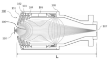
- the spherical aberration-correcting electrostatic lens 100 disclosed in Patent Document 4 is concave with respect to the sample plate 110, which is arranged to form an enlarged virtual image having negative spherical aberration.
- the magnetic field shielded ultrahigh vacuum chamber (not shown) for storing the entire spherical aberration correcting electrostatic lens 100 was large. Further, since the exit beam becomes a point source beam with a narrow solid angle due to a convergent electric field that generates positive spherical aberration, and exits from the exit port 107, for example, when projecting on a fluorescent screen for energy analysis, the exit beam 107 When the emitted electrons are analyzed with a blocking potential or a deflecting electric field (not shown) and the angular distribution is projected onto a fluorescent screen (not shown), it is necessary to converge on the exit slit once. It was difficult to make it compact.
- a normal electrostatic lens has a limit of about ⁇ 20 ° due to spherical aberration, but the sensitivity can be increased by using a spherical mesh.
- a wider capture angle can be realized by creating an optimal electric field using a plurality of electrodes.
- a lens that focuses the beam by a convergent electric field that generates a positive spherical aberration by applying the negative spherical aberration correction function of the aspherical mesh is large in size, and requires a large space when incorporated in an apparatus such as an electron spectrometer. There are inconveniences.
- an object of the present invention is to provide an electrostatic lens and a compact parallel beam generator capable of capturing charged particles emitted from a point source over a wide solid angle range and collimating the trajectory of the charged particles. And It is another object of the present invention to provide an apparatus that realizes high sensitivity and high energy resolution of photoelectron diffraction angle distribution by collimating a radiation beam having a wide solid angle. It is another object of the present invention to provide a compact parallel beam converging apparatus that can collect a parallel charged particle stream having a specific kinetic energy at one point using the electrostatic lens.
- the electrostatic lens of the present invention includes an axisymmetric or substantially axisymmetric aspherical mesh having a concave shape with respect to a point source or a condensing point, and an axisymmetric or substantially axisymmetric single lens.
- An electrostatic lens composed of one or more electrodes and having the following features (a) to (d). With such a feature, charged particles emitted from a point source can be taken in over a wide solid angle range, and the trajectory of the charged particles can be parallelized.
- the aspherical mesh is a spheroid whose major axis extends from the vicinity of the center of the mesh opening to the position of the mesh center, or a substantial spheroid whose shape near the mesh opening expands with a convex curvature inward. It is.
- the ratio of the opening radius of the mesh electrode connected to the mesh and the opening radius of the first electrode adjacent to the mesh electrode among single or plural electrodes is 1.2 or more and 1.6 or less. It is.
- the ratio of the major axis radius to the minor axis radius in the spheroid is greater than 1.0 and less than or equal to 2.0.
- D) The charged particle generated from the point source has an intake angle of ⁇ 60 °, and the locus of the charged particle is parallelized so that the deviation angle from the optical axis is ⁇ 1 ° or less.
- the number of electrodes is excluded from the mesh electrode, and the reduction ratio is the ratio of the kinetic energy at the terminal electrode to the kinetic energy at the time of generation of charged particles, and any one of the following 1) to 5): Meet. 1) When the number of electrodes is 1 and the reduction ratio is 0.1 or more and 0.3 or less, The ratio of the major axis radius to the minor axis radius in the spheroid is 1.69 or more and 1.89 or less. 2) When the number of electrodes is 2 and the reduction ratio is 0.1 or more and 0.3 or less, The ratio of the major axis radius to the minor axis radius in the spheroid is 1.56 or more and 1.76 or less.
- the ratio of the major axis radius to the minor axis radius in the spheroid is 1 when the reduction ratio is 0.01 or more and less than 0.1, regardless of the number of electrodes. It is preferably greater than 0.0 and less than 1.5.
- the substantial spheroid mesh shape has a radial deviation from the major axis of 5% or less of the radial distance compared to the spheroid shape of the same major axis radius and minor axis radius.
- an inflection point is obtained by plotting the radial shift by first-order differentiation with respect to the angle at a position where the angle between the axis connecting the point source and the mesh-shaped surface and the long axis is larger than 40 °.
- the substantial spheroid mesh shape is represented by dmesh represented by the following mathematical formula 1, which is a polynomial function.
- dmesh is the distance from the point source to the mesh surface position
- the distance d 1 is the distance from the point source to the mesh tip position on the optical axis
- the distance d 2 is from the point source to the mesh edge position.
- distance, deviation angle from the optical axis for determining the angle theta and ⁇ max each mesh surface and mesh edge position alpha is a function of the angle theta
- n is the dimension of the function
- w is the parameter a 1 ⁇ a n Is a parameter determined by.
- the parallel beam generator according to the present invention includes the above-described electrostatic lens according to the present invention and a planar collimator plate arranged coaxially with the lens. Then, the charged particle generated from the point source has an intake angle of ⁇ 60 °, and the locus of the charged particle is parallelized so that the deviation angle from the optical axis is ⁇ 1 ° or less. Then, after the trajectory of the charged particles is made parallel to the axis, the electrostatic lens and the plane collimator plate are coaxially arranged so that the charged particles are incident substantially perpendicular to the plane collimator plate. .
- the parallel beam generator of the present invention can be miniaturized, the magnetic field shielded ultra-high vacuum vacuum chamber surrounding the apparatus can be reduced, and the cost of the apparatus can be reduced.
- the electrostatic lens of the present invention charged particles emitted from a point source are captured over a wide solid angle range, and the trajectory of the charged particles is made parallel with high parallelism.
- the collimated charged particles are incident on the planar collimator plate substantially perpendicularly, thereby further improving the degree of collimation.
- the plane collimator plate takes in a beam from a thin slit or small pore provided on a flat plate, and selects only a parallel beam.
- the parallel beam generator of the present invention can analyze electrons when a negative potential is applied to an electrode and can analyze cations when a positive potential is applied.
- the electrode potential is stably controlled with an accuracy of 50 mV or less with respect to 1 kV of the DC power source.
- the planar collimator plate is characterized by functioning as a bandpass filter that selects only charged particles having a specific kinetic energy.
- a bandpass filter By functioning as a band-pass filter, the intensity distribution projected onto the screen using a fluorescent screen can be handled as it is as data of an angular distribution pattern of a specific energy.
- a planar microchannel plate in which minute photomultiplier tubes are bundled on a flat plate is further provided, and charged particles having a specific kinetic energy emitted from the planar collimator plate are amplified by an avalanche current. That's fine. High sensitivity measurement is possible by amplifying with an avalanche current.
- the planar collimator plate in the parallel beam generator of the present invention is preferably provided with pores having an aspect ratio (pore diameter to hole length) of 1: 5 to 1:20 with an aperture ratio of 50% or more.
- the greater the aspect ratio the greater the parallelism of the beam emitted from the planar collimator plate.
- the aperture ratio affects the transmittance, it is better that the aperture ratio is large.
- the aspect ratio is 1:10 and the aperture ratio is 50% or more
- the hole diameter is 50 ⁇ m with respect to the collimator diameter of 50 mm
- the upper limit of the angular resolution is 0.1 ° (the angular resolution is about 0). .1 °).
- a radius of 25 mm of the collimator corresponds to an emission angle of 50 °
- a sweeping means for sweeping the potentials of the electrodes and the planar collimator plate may be further provided.
- a fluorescent screen and camera means are further provided, and charged particles having a specific kinetic energy emitted from the above-described planar collimator plate are converted into bright spots on the fluorescent screen, and camera means. It is also possible to measure an image with. Charged particles having a specific kinetic energy are converted into bright spots on a fluorescent screen, and an image can be measured as a two-dimensional distribution pattern by a camera. Further, the planar collimator plate serves as an exit slit when projecting the angular distribution onto the fluorescent screen. A small and simple projection analyzer with high energy resolution can be realized and applied to various analyses. Thereby, it can be used as an angle distribution measurement analyzer.
- a delay line detector is further provided to detect the emission angle direction and arrival time of each charged particle having a specific kinetic energy emitted from the above-described planar collimator plate. It is also possible to measure the time-resolved image by measuring individually with the instrument.
- the emission angle direction and arrival time of each charged particle of specific kinetic energy emitted from the planar collimator plate can be individually measured by the delay line detector. Time-resolved image measurement can be performed. Accordingly, there is an advantage that time information indicating when each particle is emitted after excitation is obtained simultaneously with measurement of the emission angle distribution of the charged particles.
- the energy resolution of the bandpass filter by the plane collimator plate is a relative value, and in the case of 1% energy resolution, the resolution is 1 eV for 100 eV and 10 eV for 1 keV.
- the energy resolution of the measurement by lock-in detection is an absolute value determined by the modulation electric field.
- the resolution is 0.1% for 100 eV and 0.01% for 1 keV.
- a modulation electric field of 1 V to 10 V is used in lock-in detection.
- the band-pass method using the planar collimator plate in the present invention a high S / B ratio and high amplification are possible, so that the modulation electric field can be reduced to 100 mV.
- the above-mentioned angle distribution measuring and analyzing apparatus includes an electron spectroscopic apparatus, an electron diffractometer, a photoelectron spectroscope, a photoelectron diffractometer, a positron in which the parallel beam generator of the present invention is incorporated as an emission angle distribution analyzer of charged particle energy.
- the parallel beam generator of the present invention described above is incorporated as a single-energy large-diameter parallel ion beam source, and performs ion etching or ion sputtering.
- the focused ion beam is scanned two-dimensionally or unfocused to increase the beam diameter. In either case, the beam is located away from the center.
- the pattern processing is performed using a mask, for example, the end portion is bent and it is difficult to form a high aspect ratio.
- the parallel beam generator of the present invention can capture ions in a wide solid angle range and generate a large-diameter parallel ion beam with a single kinetic energy.
- the surface irradiation with the generated large-diameter parallel ion beam In the pattern processing using a mask, the end portion is not sagged, a high aspect ratio can be formed, and the shape can be precisely controlled etching.
- the wide solid angle X-ray detector according to the present invention generates a flat collimator plate with a negative potential on the flat collimator plate and a positive potential on the fluorescent screen in the parallel beam generator of the present invention provided with a fluorescent screen and camera means. It amplifies electrons. According to this configuration, a wide solid angle X-ray detector can be realized.
- a parallel beam focusing device is provided.
- the parallel beam converging device is composed of the above-described electrostatic lens of the present invention and a planar collimator plate arranged coaxially with the electrostatic lens, and is a specific kinetic energy charged particle that is incident substantially perpendicular to the planar collimator plate.
- the electrostatic lens and the planar collimator plate are arranged coaxially so that the locus after the emission of the light is condensed at the condensing point by the electrostatic lens.
- the parallel beam generator of the present invention when the entrance and the exit are reversed, the charged particle flow in a specific direction is taken out by the collimator plate, and only the particles having a specific energy are collected at a single point by the electrostatic lens. It can be used as a parallel beam focusing device that measures
- the plane collimator plate in the parallel beam converging apparatus may be configured such that pores having an aspect ratio (ratio of pore diameter to hole length) of 1: 5 to 1:20 are provided with an aperture ratio of 50% or more. good.
- the charged particle flow direction / energy measuring apparatus includes a plurality of parallel beam converging apparatuses according to the other aspects of the present invention described above, and a plane collimator plate that selects only charged particles having a specific kinetic energy.
- the charged particle flow in a specific direction is taken out by a plane collimator plate, and only the particles having a specific energy are collected at one point by an electrostatic lens to measure the energy intensity.
- the parallel beam generator of the present invention there is an effect that the intensity angle distribution of charged particles having a specific kinetic energy emitted from a sample can be projected on a plane up to a solid angle of about ⁇ 60 °. Since the sensitivity is proportional to the solid angle of capture, the sensitivity and function can be greatly improved. That is, it becomes possible to collimate a radiation beam with a wide solid angle, and there is an effect that high sensitivity and high energy resolution of the photoelectron diffraction angle distribution can be achieved.
- the energy resolution of the planar collimator plate can be improved by making the excitation beam minute. For example, when a convergent beam of 100 ⁇ m or less is used as the excitation beam, the energy resolution of 1. There is an effect that 0 to 0.5% can be achieved.
- the parallel beam generator of the present invention can be miniaturized and can be easily incorporated into other analyzers. For example, when combined with an SEM (scanning electron microscope), it is element-selective that selects only specific energy. Crystal structure observation can be realized.
- the charged particle flow in a specific direction is taken out by the collimator plate, and only particles having a specific energy are statically extracted.
- the intensity can be measured by collecting light at one point with an electric lens.
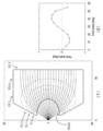
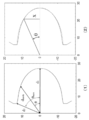
- Configuration diagram of parallel beam generator of embodiment 1 Explanatory diagram of the angle from the point source and the charged particle trajectory Illustration of electrode arrangement Illustration of shape of aspherical mesh Explanatory drawing of the trajectory of electrons of different energy (1) Explanatory diagram of the trajectory of electrons of different energy (2) Diagram showing the transmittance of a flat collimator plate Explanatory diagram of electron trajectories at different emission positions Explanatory drawing about the difference in the number of electrodes in an electrostatic lens Configuration of angle distribution measurement analyzer according to embodiment 4 Configuration diagram of wide solid-angle X-ray detector of Example 5 Trajectory and parallelism of charged particles of electrostatic lens (number of electrodes: 1) in Example 7 Trajectory and parallelism of charged particles of electrostatic lens (number of electrodes: 2) in Example 7 Trajectory and parallelism of charged particles of electrostatic lens (number of electrodes: 3) in Example 7 Trajectory and parallelism of charged particles of electrostatic lens (number of electrodes: 4) in Example 7 Trajectory and parallel
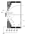
- FIG. 1 shows an embodiment of the parallel beam generator of the present invention.
- the parallel beam generator of the present invention comprises an electrostatic lens of the present invention comprising an axisymmetric aspherical mesh 2 having a concave surface with respect to a point source 7 and five axially symmetric electrodes (10 to 14). It is composed of a flat collimator plate 3 arranged coaxially with the lens, a fluorescent screen 4, and a magnetic shielding cover 8 for storing them.
- charged particles electrons or ions
- the charged particle generated from the point source 7 has an uptake angle of about ⁇ 58 °, and the aspherical mesh 2 is meshed so that the trajectory of the charged particle is parallelized by the electrostatic lens.
- the shape and potential and arrangement of the five electrodes (10 to 14) are adjusted.
- the electrostatic lens and the plane collimator plate 3 are arranged coaxially so that the charged particles are incident perpendicularly to the plane collimator plate 3.
- the excitation beam is applied to the sample plate 20 by the excitation beam guide tube 21 so that there is no interference with charged particles generated from the point source 7.
- the excitation beam guide tube 21 is arranged with respect to the sample plate 20 so that the incident angle of the excitation beam is 75 ° or more.
- a fluorescent screen 4 is provided, and charged particles having a specific kinetic energy emitted from the flat collimator plate 3 are converted into bright spots by the fluorescent screen 4, and this is imaged by a camera and the energy distribution is measured. can do.
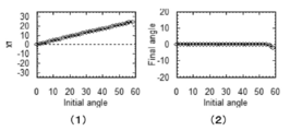
- the horizontal axis (Initial angle) in FIGS. 2 (1) and (2) indicates the capture angle (solid angle) of charged particles emitted from the point source, and the vertical axis in FIG.
- the distance (Xf) and the vertical axis (Final angle) in FIG. 2B indicate the angle of the trajectory of the charged particles incident on the planar collimator plate 3. Both angles are from an axis perpendicular to the sample plate.
- the range of the capture angle that can be collimated is 0 to ⁇ 58 °
- the horizontal axis (Initial angle) is 0 to 60 ° with respect to the charged particles emitted from the point source.
- the angle of the trajectory of the charged particles incident on the planar collimator plate 3 is 0 ° (that is, parallel to the axis) up to about 58 °, but when it exceeds 58 °, the angle deviates from 0 ° and is parallel. It has not been shown.
- the electron beam emitted from the point source 7 can be collimated when the energy of the electron beam is 1000 eV and the capture angle range is 0 to ⁇ 58 °.
- Each of the electrodes 10 to 15 is a coaxial ring-shaped electrode.
- the electrode 10 is connected to the aspherical mesh 2 and is connected to the ground so as to be 0V. This is because the potential is the same as that of the sample plate 20.
- the three electrodes 11 to 13 are sequentially arranged so as to be away from the point source 7 and the length of the electrodes is shortened so that the tip of the electrode is arranged outside the outer periphery of the electron beam. .
- the electrode 14 is disposed at the most distant position and has a shape extending in the axial direction.
- the electrode 15 is connected to the planar collimator plate 3.
- Electrode 15 is ⁇ 950 ⁇ V.
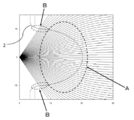
- the aspherical mesh 2 is a substantially spheroid (A in the figure) having a major axis from the vicinity of the center of the mesh opening to the position of the mesh center, and the vicinity of the mesh opening (B in the figure) is inwardly convex.
- the shape of the mesh is not spherical but is close to a spheroid with a long axis in the axial direction It has a shape.
- FIG. 5 shows an electron trajectory with an energy of 1030 eV
- FIG. 6 shows an electron trajectory with an energy of 970 eV.
- the potential of each electrode is the same as in FIG. 1, and the electrode 10 is 0V, the electrode 11 is -520V, the electrode 12 is -780V, the electrode 13 is -888V, the electrode 14 is -914.5V, and the electrode 15 is- 950V.
- the beam that expands more than the parallel when the electron energy increases. On the other hand, if the electron energy decreases, the beam converges rather than parallel.
- FIG. 7 (1) shows the transmittance (in the case of a point source) of a planar collimator plate provided with pores having an aspect ratio (ratio of pore diameter to pore length) of 1: 5.
- 7 (2) to (6) are provided with pores having aspect ratios (ratio of pore diameter to pore length) of 1:10, 1:20, 1:30, 1:40, and 1:50, respectively.
- the transmittance of a flat collimator plate (in the case of a point source) is shown.
- the emission angle polar angle
- the transmittance with respect to other than a specific energy is suppressed, and it is shown that the function of a band-pass filter having sufficient energy resolution can be obtained only by the planar collimator plate.
- FIG. 8 shows that the electron beam energy of 1000 eV, the electrode arrangement and the potential are the same in the parallel beam generator shown in FIG.
- the electron trajectory is shown (with the position of the point source being 0, ⁇ 0.5 mm, ⁇ 1.0 mm).
- the diffracting surface of electrons incident on the planar collimator plate is not a flat surface but a curved surface.
- the convergence angle of the electron beam on the axis is ⁇ 9.7 °, and it can be seen that not only the energy but also the position is selected.
- the parallel beam generator of the present embodiment when a convergent beam of 100 ⁇ m or less is used as an excitation beam, an energy resolution of 1.0 to 0.5% can be achieved.
- an electron diffraction pattern in a region of 100 ⁇ m or less can be selectively measured even when the beam diameter is large.
- FIGS. 9 (1) to 9 (5) show the trajectories of electrons emitted from a point source by incident light having an incident angle of 75 ° in an electrostatic lens using an aspherical mesh having the same shape. This is because incident light with an incident angle of 75 ° does not interfere with the path of outgoing electrons.
- 9 (1) to 9 (5) are different in the number of electrodes of the electrostatic lens.
- the mesh electrode connected to the aspherical mesh is fixed to the ground potential, and a single or a plurality of negative potential electrodes are arranged. That is, the electrodes other than the mesh electrode have a negative potential.
- FIG. 9 (1) has 1 electrode
- FIG. 9 (2) has 2 electrodes
- FIG. 9 (3) has 3 electrodes
- FIG. 9 (4) has 5 electrodes
- FIG. 9 (5) has The number of electrodes is six.
- the mesh electrode fixed to the ground potential is excluded from the number of electrodes.
- five or more electrodes shown in FIG. 9 (4) or FIG. 9 (5) are required.
- the shape of the aspherical mesh was optimized according to the examples having different numbers of electrodes. As the number of electrodes increases, the ratio of the major axis to the minor axis decreases and approaches a spherical surface. By introducing a shape that expands with a convex curvature inside the vicinity of the mesh opening, it is possible to ensure parallelization up to the vicinity of an emission angle of 60 ° from the point source.
- Ion Etching equipment is used to manufacture semiconductor microelements, remove coating films from cutting tools, parts, etc., remove fine burrs, process tip shapes, remove dirt adhering to metal material surfaces, and activate metal material surfaces.
- the ion beam emitted from the ion beam source is chemically reacted with atoms on the surface of the etching material, or the surface of the etching material is physicochemically etched to etch the shape of the material surface.
- the parallel beam generator of Example 1 or Example 2 ions can be taken in a wide solid angle range and a large-aperture parallel ion beam with a single kinetic energy can be generated. That is, by using the parallel beam generation apparatus of the first embodiment or the second embodiment, the ion beam source of the ion etching apparatus can be a single energy large-diameter parallel ion beam source. As a result, the ion beam hits the sample surface perpendicularly even at a location away from the center of the ion beam, so that the edge is not sagged even during pattern processing using a mask, and a high aspect ratio can be molded. Precision controlled etching of the shape is possible. In addition, when single energy ions are used, the etching rate can be easily controlled, and the thickness of the thin film to be etched can be controlled.
- FIG. 10 shows a configuration diagram of the angle distribution measurement analyzer.
- the angular distribution measurement analyzer according to the present embodiment includes a blocking potential grid 32 and a planar microchannel plate 31 provided between the planar collimator plate 3 and the fluorescent screen 4 in the parallel beam generation apparatus according to the first embodiment.
- the change of the current due to the charged particles passing through the grid 32 is detected by the lock-in modulation electric field 30 by changing the DC voltage.
- the energy resolution ( ⁇ E / E) of specific kinetic energy charged particles emitted from the planar collimator plate 3 can be improved to 0.1 to 0.01%.
- the S / B ratio (Signal / Background ratio) is poor, and it is difficult to amplify with a flat microchannel plate.
- the modulation electric field uses 1V to 10V.
- the band pass filter function by the planar collimator plate 3 enables high S / B ratio and high amplification, and the modulation electric field can be reduced to 100 mV.
- signal amplification can be performed using a planar microchannel plate.
- the energy resolution of the bandpass filter by the plane collimator plate 3 is a relative value, and in the case of 1% energy resolution, the resolution is 1 eV for 100 eV and 10 eV for 1 keV.
- the energy resolution of the measurement by lock-in detection is an absolute value determined by the modulation electric field. Therefore, in the case of a modulation electric field of 100 mV, the resolution is 0.1% for 100 eV and 0.01% for 1 keV. is there.
- FIG. 11 shows a configuration diagram of a wide solid angle X-ray detector.
- the wide solid angle X-ray detector according to the present embodiment amplifies electrons generated by the flat collimator plate 3 in the parallel beam generator of the first embodiment with the flat collimator plate 3 set to a negative potential and the fluorescent screen 4 set to a positive potential.
- the X-ray detector will be described.
- Auger electrons with a short mean free path are emitted from the vicinity of the sample surface, and fluorescent X-rays with a long mean free path are emitted also from the inside of the crystal.
- Auger electrons and fluorescent X-rays are emitted simultaneously in proportion to the X-ray absorption intensity.
- Auger electron yield method X-ray absorption measurement and fluorescent X-rays have been performed using another detector. Yield method X-ray absorption measurements have been performed. Since fluorescent X-rays travel in a straight line regardless of the electric field, the conventional blocking potential electron analyzer using a spherical mesh cannot reach all the fluorescent screen and be removed.
- the plane collimator plate 3 by combining the plane collimator plate 3 and the blocking potential grid 32, it is possible to remove the fluorescent X-rays when analyzing the Auger electrons by preventing the path of the fluorescent X-rays proceeding linearly.
- a negative potential is applied to the planar collimator plate 3 to block Auger electrons
- a positive potential is applied to the blocking potential grid 32 and the fluorescent screen 4 to thereby increase the signal intensity of fluorescent X-rays.
- the planar collimator plate 3 can convert it into electrons, and can be used as a wide solid angle X-ray detector.
- Auger electrons and fluorescent X-rays can be measured with the same detector by simply reversing the applied electric field, and information on X-ray absorption spectroscopy depending on the surface and the depth inside the crystal can be obtained. It will be a detector.
- the flat microchannel plate 31 is provided to amplify the electrons.
- a blocking potential grid 32 is provided in the configuration of FIG. 11, the electrodes 11 to 14 are connected to the ground and the electrode 15 is set to a negative potential, but all of the electrodes 11 to 15 may be set to a negative potential.
- the parallel beam generator shown in FIG. 1 is reversed and the flow of charged particles in a specific direction is taken out by the flat collimator plate 3 and only the specific energy particles are collected at one point by the electrostatic lens and the intensity is measured.
- a parallel beam focusing device that can be used will be described. Similar to the configuration shown in FIG.
- the parallel beam converging apparatus includes an axisymmetric aspherical mesh 2 having a concave shape with respect to the focal point and an electrostatic lens composed of a single or a plurality of axisymmetric electrodes,
- the trajectory after the emission of specific kinetic energy charged particles that are made up of a plane collimator plate 3 and coaxially arranged on the plane collimator plate 3 and enter the plane collimator plate 3 substantially perpendicularly becomes a condensing point by the electrostatic lens.
- the shape of the aspherical mesh 2 and the potential and arrangement of the ground electrode 10 and the application electrodes (11 to 15) are adjusted so as to collect light.
- the entrance / exit is reversed compared to the parallel beam generating apparatus.
- the fluorescent screen 4 and the excitation beam guiding tube 21 are unnecessary as compared with the case of the parallel beam generating apparatus.
- the potentials of the electrodes 10 to 15 are the same as those in Example 1.
- the electrode 10 is 0 V (fixed to the ground potential)
- the electrode 11 is ⁇ 520 V
- the electrode 12 is ⁇ 780 V
- the electrode 13 is ⁇ 888 V
- the electrode 14 is -914.5V
- the electrode 15 is -950V.
- the planar collimator plate 3 functions as a band-pass filter that selects only charged particles having a specific kinetic energy, and takes out a charged particle flow in a specific direction incident on the planar collimator plate.
- the plane collimator plate 3 is provided with pores having an aspect ratio (ratio of pore diameter to pore length) of 1:10 at an aperture ratio of 50% or more.
- the shape of the aspherical mesh is a substantially spheroid whose major axis extends from the vicinity of the center of the mesh opening to the position of the center of the mesh, and the vicinity of the mesh opening expands with a convex curvature inward.
- the optical system includes a plurality of electrodes, and at least one of them is provided with an aspherical mesh having a concave shape with respect to the object surface.
- This aspherical mesh captures charged particles emitted from a point source over a wide solid angle, and parallelizes the trajectories of the captured charged particles with high parallelism.
- the shape of the aspherical mesh is such that the charged particle generated from the point source has an intake angle of ⁇ 60 °, and the locus of the charged particle is parallelized so that the deviation angle from the optical axis is ⁇ 1 ° or less. If parallelism is not required, the mesh shape can be designed with a spheroid. Further, regarding the number of electrodes excluding the mesh electrode fixed at the ground potential, at least one may be used when the taking-in angle to be parallelized may be about ⁇ 50 ° or less or when a very high parallelism is not required. . In the following, the trajectory and parallelism of the charged particles will be described for an electrostatic lens having an aspherical mesh shape designed as a spheroid and having 1 to 5 electrodes.
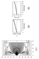
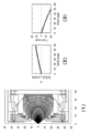
- FIG. 12 shows an example of an electrostatic lens having one electrode.
- the shape of the aspherical mesh is designed by a spheroid, and the ratio of the major axis radius to the minor axis radius (hereinafter abbreviated as the major axis minor axis ratio) in the spheroid is 1.79.
- the applied voltage of each electrode is 0V for the mesh electrode (G) and -775V for the first electrode (EL1) with respect to 1 keV electrons.
- FIG. 12A is a cross-sectional view including the optical axis, and the inner surface shape of the electrode and the aspherical mesh is represented by a thick solid line.
- the dotted line represents the equipotential line, and the thin solid line represents the trajectory of the charged particle.
- the incident angle is drawn from ⁇ 55 ° to 55 ° in 5 ° steps.
- a spheroidal mesh is connected to the mesh electrode (G).
- the major axis / minor axis ratio of the spheroid is 1.79.
- the terminal portion of the first electrode (EL1) corresponds to a planar collimator.
- the voltages applied to the mesh electrode (G) and the first electrode (EL1) are 0 V and ⁇ 775 V, respectively, for 1 keV electrons.
- 12 (2) is a graph in which the angle (angle from the optical axis) at the end of the trajectory of the charged particle shown in FIG. 12 (1) is plotted against the incident angle (Initial angle) to the aspherical mesh. It is. It can be seen that charged particles having an incident angle of ⁇ 55 ° to 55 ° are collimated to an angle of about 0.8 ° with the optical axis.
- R2 / R1 is about 1.2 to 1.6. This is a preferred embodiment.
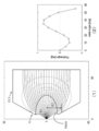
- FIG. 13 is an example of an electrostatic lens having two electrodes.
- the shape of the aspherical mesh is designed by a spheroid, and the major axis / minor axis ratio of the spheroid is 1.66.
- the applied voltage of each electrode is 0V for the mesh electrode (G), -680V for the first electrode (EL1), and -820V for the second electrode (EL2) with respect to 1 keV electrons.
- the electrostatic lens with two electrodes shown in FIG. 13 (1) is obtained by dividing the first electrode (EL1) in FIG. 12 (1) into two on the mesh electrode (G) side. 13 (1) and 12 (1) are compared with respect to the trajectory of the charged particles.
- FIG. 13 is an example of an electrostatic lens having two electrodes.
- the shape of the aspherical mesh is designed by a spheroid, and the major axis / minor axis ratio of the spheroid is 1.66.
- the applied voltage of each electrode is 0V for the
- FIG. 13 (1) is a plot of the angle at the end point of the trajectory shown in FIG. 13 (1) (angle from the optical axis) with respect to the incident angle.
- the incident angle is ⁇ 55 ° to 55 °. It can be seen that the charged particles of ° are collimated to an angle of about 0.6 ° with the optical axis.
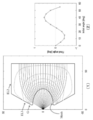
- FIG. 14 is an example of an electrostatic lens having three electrodes.
- the shape of the aspherical mesh is designed by a spheroid, and the major axis / minor axis ratio of the spheroid is 1.62.
- the applied voltage of each electrode is 0V for the mesh electrode (G), -625V for the first electrode (EL1), -745V for the second electrode (EL2), and -832V for the third electrode (EL3) for 1 keV electrons. It is.
- the electrostatic lens with three electrodes shown in FIG. 14 (1) is obtained by dividing the first electrode (EL1) in FIG. 12 (1) into three on the mesh electrode (G) side. 14 (1) and 12 (1) are compared with respect to the trajectory of the charged particles.
- FIG. 14 (1) is obtained by dividing the first electrode (EL1) in FIG. 12 (1) into three on the mesh electrode (G) side. 14 (1) and 12 (1) are compared with respect to the trajectory of the charged particles.
- FIG. 14 (1) is a plot of the angle at the end point of the trajectory shown in FIG. 14A (the angle from the optical axis) with respect to the incident angle.
- the incident angle is ⁇ 55 ° to 55 °. It can be seen that the charged particles of ° are collimated to an angle of about 0.6 ° with the optical axis.
- a mesh having a smaller major axis / minor axis ratio is advantageous in realizing a high transmittance.
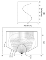
- FIG. 15 is an example of an electrostatic lens having four electrodes.
- the shape of the aspherical mesh is designed by a spheroid, and the major axis / minor axis ratio of the spheroid is 1.59.
- the voltage applied to each electrode is 0V for the mesh electrode (G), -620V for the first electrode (EL1), -750V for the second electrode (EL2), and -750V for the third electrode (EL3) for 1 keV electrons. 830V, the fourth electrode (EL4) is -850V.
- the electrostatic lens with four electrodes shown in FIG. 15A is obtained by dividing the third electrode (EL3) in FIG. 14A into two at the cylindrical portion.
- FIG. 16 is an example of an electrostatic lens having five electrodes.
- the shape of the aspherical mesh is designed by a spheroid, and the major axis / minor axis ratio of the spheroid is 1.49.
- the voltage applied to each electrode is 0V for the mesh electrode (G), -590V for the first electrode (EL1), -730V for the second electrode (EL2), and -730V for the third electrode (EL3) for 1 keV electrons. 860V, the fourth electrode (EL4) is -880V, and the fifth electrode (EL5) is -900V.
- the third electrode (EL3) in FIG. 14 (1) is divided into two parts at the cylindrical part, and the terminal part is further divided from the cylindrical part. This is an electrode (EL5).
- FIG. 17 is an example of an electrostatic lens having six electrodes, similar to FIG.
- the shape of the aspherical mesh is designed by a spheroid, the major axis / minor axis ratio in the spheroid is 1.37, and the applied voltage of each electrode is 1 keV electron
- Mesh electrode (G) is 0V
- first electrode (EL1) is -580V
- second electrode (EL2) is -730V
- third electrode (EL3) is -870V
- fourth electrode (EL4) is -919V
- fifth The electrode (EL5) is -950V.
- the number of electrodes is the same, but the rate of deceleration is different.
- the ratio (Ef / Ei) between the kinetic energy (Ef) at the end portion and the kinetic energy (Ei) at the time of incidence is defined as a reduction ratio.
- the reduction ratios in FIGS. 15 to 17 are 0.15, 0.1, and 0.05, respectively.
- the cylindrical portion is preferably constituted by a plurality of electrodes as shown in FIGS. 15 to 17, the major axis / minor axis ratios of the spheroidal surface are 1.59, 1.49, and 1.37, respectively.
- the appropriate mesh shape is a spheroid with a smaller major axis / minor axis ratio. 12 to 17, the angle between the obtained charged particle trajectory and the optical axis is about 0.3 to 0.8 °, but this parallelism is not appropriate for the aspherical mesh shape, not the spheroid. It can be greatly improved by expressing it by a simple polynomial function. This will be described in Example 8 below.
- the incident angle of the charged particles generated from the point source is ⁇ 60 °
- the locus of the charged particles is parallelized so that the deviation angle from the optical axis is ⁇ 1 ° or less.
- the mesh shape is not designed with a spheroid, but a shape different from the spheroid. Use an aspherical mesh.
- the aspherical mesh shape has a radial deviation from the major axis of 5% or less of the radial distance compared to the shape of a spheroid having the same major axis radius and minor axis radius, and There is an inflection point that is obtained by first-order differentially plotting the radial deviation with respect to the angle at a position where the angle between the axis connecting the mesh-shaped surface and the long axis is larger than 40 °.
- the aspherical mesh shape can be represented by dmesh represented by the following mathematical function expression.
- the distance dmesh from the point source to the mesh surface position is the distance of the distance d 1 from the point source to the mesh tip position on the optical axis
- the distance d 2 is the distance from the point source to the edge position of the mesh.
- angles ⁇ and ⁇ max indicate deviation angles from the optical axis for determining the mesh surface and mesh edge positions, respectively.
- alpha is a function of the angle theta
- n is the dimension of the function
- w is a parameter determined by the parameter a 1 ⁇ a n.
- FIG. 18 is an example of an electrostatic lens in which the shape of the aspherical mesh is designed using the above polynomial function.
- the configuration of the electrodes in the electrostatic lens of this example is the same as that of the two-electrode electrostatic lens shown in FIG. 13, and the applied voltage of each electrode is 1 keV electron.
- the mesh electrode (G) is 0V
- the first electrode (EL1) is ⁇ 772V
- the second electrode (EL2) is ⁇ 796V.
- the dimension n of the polynomial function is 5, and the value of each parameter is as shown in Table 1 below.
- Fig. 18 (2) is a plot of the angle at the end of the trajectory shown in Fig. 18 (1) (angle from the optical axis) against the incident angle.
- the angle formed with the optical axis of the trajectory of the charged particles is a parallel degree of about 0.5 °, whereas FIG. Then, it can be seen that the angle between the activation of the charged particles and the optical axis is a very high parallelism of about ⁇ 0.01 ° over an incident angle of ⁇ 45 ° to 45 °.
- FIG. 19 (2) is a comparison between the aspherical mesh shape shown in FIG. 18 and the aspherical mesh shape (spheroid surface) shown in FIG.
- the former is indicated by a solid line and the latter is indicated by a dotted line.
- the deviation is about 5% or less.
- the result of calculating the first derivative with respect to the angle ⁇ of x for each shape is shown in FIG.
- FIG. 20 is a diagram for explaining the characteristics of the non-spherical mesh shape of the electrostatic lens of this example.
- 20A corresponds to the aspherical mesh shape shown in FIG. 12 (dotted line in FIG. 19)
- FIG. 20B corresponds to the aspherical mesh shape shown in FIG. 18 (solid line in FIG. 19).
- Yes In the case of the aspherical mesh-shaped spheroid shown in FIG. 12, there is no inflection point, and the monotonous decreasing function is shown in FIG.
- the aspherical mesh shape shown in FIG. 18 there is an inflection point.
- the aspherical mesh shape is It can be a spheroid.
- the ratio (R2 / R1) of the opening radius R1 of the mesh electrode connected to the aspherical mesh and fixed at the ground potential to the opening radius R1 of the first electrode adjacent to the mesh electrode is 1.2. It is preferably 1.6 or less.
- the major axis / minor axis ratio of the spheroid is 1.69 or more and 1.89 or less. Is preferred.
- the major axis / minor axis ratio of the spheroid is preferably 1.56 or more and 1.76 or less.
- the major axis / minor axis ratio of the spheroid is preferably 1.52 or more and 1.72 or less.
- the major axis / minor axis ratio of the spheroid is preferably 1.49 or more and 1.69 or less.
- the major axis / minor axis ratio of the spheroid is preferably 1.39 or more and 1.59 or less.
- the major axis / minor axis ratio of the spheroid is preferably greater than 1.0 and less than 1.5.
- the aspherical mesh shape is not a spheroid, and the deviation from the spheroid is about 5% or less.
Landscapes
- Chemical & Material Sciences (AREA)
- Analytical Chemistry (AREA)
- Physics & Mathematics (AREA)
- Optics & Photonics (AREA)
- Engineering & Computer Science (AREA)
- Plasma & Fusion (AREA)
- Health & Medical Sciences (AREA)
- Life Sciences & Earth Sciences (AREA)
- Biochemistry (AREA)
- General Health & Medical Sciences (AREA)
- General Physics & Mathematics (AREA)
- Immunology (AREA)
- Pathology (AREA)
- Analysing Materials By The Use Of Radiation (AREA)
Abstract
Priority Applications (3)
| Application Number | Priority Date | Filing Date | Title |
|---|---|---|---|
| EP16824509.0A EP3324421A4 (fr) | 2015-07-15 | 2016-07-13 | Lentille électrostatique, et dispositif de génération de faisceau parallèle et dispositif de convergence de faisceau parallèle utilisant la lentille électrostatique et un collimateur |
| US15/744,769 US10614992B2 (en) | 2015-07-15 | 2016-07-13 | Electrostatic lens, and parallel beam generation device and parallel beam convergence device which use electrostatic lens and collimator |
| JP2017528715A JP6757036B2 (ja) | 2015-07-15 | 2016-07-13 | 静電レンズ、並びに、該レンズとコリメータを用いた平行ビーム発生装置及び平行ビーム収束装置 |
Applications Claiming Priority (2)
| Application Number | Priority Date | Filing Date | Title |
|---|---|---|---|
| JP2015-141687 | 2015-07-15 | ||
| JP2015141687 | 2015-07-15 |
Publications (1)
| Publication Number | Publication Date |
|---|---|
| WO2017010529A1 true WO2017010529A1 (fr) | 2017-01-19 |
Family
ID=57758238
Family Applications (1)
| Application Number | Title | Priority Date | Filing Date |
|---|---|---|---|
| PCT/JP2016/070744 Ceased WO2017010529A1 (fr) | 2015-07-15 | 2016-07-13 | Lentille électrostatique, et dispositif de génération de faisceau parallèle et dispositif de convergence de faisceau parallèle utilisant la lentille électrostatique et un collimateur |
Country Status (4)
| Country | Link |
|---|---|
| US (1) | US10614992B2 (fr) |
| EP (1) | EP3324421A4 (fr) |
| JP (1) | JP6757036B2 (fr) |
| WO (1) | WO2017010529A1 (fr) |
Cited By (5)
| Publication number | Priority date | Publication date | Assignee | Title |
|---|---|---|---|---|
| DE102017130072A1 (de) * | 2017-12-15 | 2019-06-19 | Leibniz-Institut Für Festkörper- Und Werkstoffforschung Dresden E.V. | Impulsauflösendes Photoelektronenspektrometer und Verfahren zur impulsauflösenden Photoelektronenspektroskopie |
| JP2021057178A (ja) * | 2019-09-30 | 2021-04-08 | 日本電子株式会社 | インプットレンズおよび電子分光装置 |
| WO2021125297A1 (fr) | 2019-12-17 | 2021-06-24 | 大学共同利用機関法人自然科学研究機構 | Lentille de cathode de réglage d'aberration sphérique, lentille électrostatique de correction d'aberration sphérique, spectroscope d'électrons et microscope électronique à photoémission |
| US20210193448A1 (en) * | 2018-05-09 | 2021-06-24 | National University Corporation NARA Institute of Science and Technology | Variable reduction ratio spherical aberration correction electrostatic lens, wide angle energy analyzer, and two-dimensional electron spectrometer |
| CN117113794A (zh) * | 2023-10-23 | 2023-11-24 | 之江实验室 | 磁约束带电粒子成像系统中反角度准直器的设计方法 |
Families Citing this family (3)
| Publication number | Priority date | Publication date | Assignee | Title |
|---|---|---|---|---|
| US11011343B2 (en) * | 2019-07-15 | 2021-05-18 | Applied Materials, Inc. | High-current ion implanter and method for controlling ion beam using high-current ion implanter |
| US11562879B2 (en) * | 2020-09-15 | 2023-01-24 | Nuflare Technology, Inc. | Low-blur electrostatic transfer lens for multi-beam electron gun |
| US11749495B2 (en) * | 2021-10-05 | 2023-09-05 | KLA Corp. | Bandpass charged particle energy filtering detector for charged particle tools |
Citations (4)
| Publication number | Priority date | Publication date | Assignee | Title |
|---|---|---|---|---|
| JP2001035434A (ja) * | 1999-06-25 | 2001-02-09 | Staib Instr Gmbh | エネルギ分解及び角度分解電子分光用の結像装置、その方法及び分光器 |
| JP2004507861A (ja) * | 1999-12-13 | 2004-03-11 | セメクイップ, インコーポレイテッド | イオン注入イオン源、システム、および方法 |
| WO2008013232A1 (fr) * | 2006-07-26 | 2008-01-31 | National University Corporation NARA Institute of Science and Technology | Lentille de type à modération de correction d'aberration sphérique, système de lentille à correction d'aberration sphérique, dispositif de spectroscopie électronique, et microscope électronique optique |
| US20100163725A1 (en) * | 2007-01-15 | 2010-07-01 | Ian Richard Barkshire | Charged particle analyser and method |
Family Cites Families (7)
| Publication number | Priority date | Publication date | Assignee | Title |
|---|---|---|---|---|
| US4764673A (en) * | 1987-04-30 | 1988-08-16 | Kevex Corporation | Electric electron energy analyzer |
| US6150089A (en) * | 1988-09-15 | 2000-11-21 | New York University | Method and characterizing polymer molecules or the like |
| US7928381B1 (en) * | 2006-05-19 | 2011-04-19 | Apparati, Inc. | Coaxial charged particle energy analyzer |
| JP5242937B2 (ja) * | 2007-04-10 | 2013-07-24 | 株式会社Sen | イオン注入装置及びイオン注入方法 |
| WO2014185074A1 (fr) * | 2013-05-15 | 2014-11-20 | Okinawa Institute Of Science And Technology School Corporation | Diffraction d'electrons de faible energie (leed) pour meb |
| CN104345331B (zh) * | 2013-07-24 | 2017-04-19 | 中国科学院上海微系统与信息技术研究所 | 图像型电子自旋分析器 |
| DE102017130072B4 (de) * | 2017-12-15 | 2021-05-20 | Leibniz-Institut Für Festkörper- Und Werkstoffforschung Dresden E.V. | Impulsauflösendes Photoelektronenspektrometer und Verfahren zur impulsauflösenden Photoelektronenspektroskopie |
-
2016
- 2016-07-13 US US15/744,769 patent/US10614992B2/en active Active
- 2016-07-13 EP EP16824509.0A patent/EP3324421A4/fr not_active Withdrawn
- 2016-07-13 JP JP2017528715A patent/JP6757036B2/ja active Active
- 2016-07-13 WO PCT/JP2016/070744 patent/WO2017010529A1/fr not_active Ceased
Patent Citations (4)
| Publication number | Priority date | Publication date | Assignee | Title |
|---|---|---|---|---|
| JP2001035434A (ja) * | 1999-06-25 | 2001-02-09 | Staib Instr Gmbh | エネルギ分解及び角度分解電子分光用の結像装置、その方法及び分光器 |
| JP2004507861A (ja) * | 1999-12-13 | 2004-03-11 | セメクイップ, インコーポレイテッド | イオン注入イオン源、システム、および方法 |
| WO2008013232A1 (fr) * | 2006-07-26 | 2008-01-31 | National University Corporation NARA Institute of Science and Technology | Lentille de type à modération de correction d'aberration sphérique, système de lentille à correction d'aberration sphérique, dispositif de spectroscopie électronique, et microscope électronique optique |
| US20100163725A1 (en) * | 2007-01-15 | 2010-07-01 | Ian Richard Barkshire | Charged particle analyser and method |
Non-Patent Citations (4)
| Title |
|---|
| MATSUDA, H. ET AL.: "Approach for simultaneous measurement of two-dimensional angular distribution of charged particles: Spherical aberration correction using an ellipsoidal mesh", PHYSICAL REVIEW E, vol. 71, 28 June 2005 (2005-06-28), pages 066503, XP003020696 * |
| MATSUDA, H. ET AL.: "Development of display-type ellipsoidal mesh analyzer: Computational evaluation and experimental validation", JOURNAL OF ELECTRON SPECTROSCOPY AND RELATED PHENOMENA, vol. 195, 13 May 2014 (2014-05-13), pages 382 - 398, XP055345978 * |
| See also references of EP3324421A4 * |
| TÓTH, LÁSZLÓ ET AL.: "Details of 1 PI sr wide acceptance angle electrostatic lens for electron energy and two-dimensional angular distribution analysis combined with real space imaging", NUCLEAR INSTRUMENTS AND METHODS IN PHYSICS RESEARCH SECTION A, vol. 661, no. 1, 21 September 2011 (2011-09-21), pages 98 - 105, XP028103472 * |
Cited By (11)
| Publication number | Priority date | Publication date | Assignee | Title |
|---|---|---|---|---|
| DE102017130072A1 (de) * | 2017-12-15 | 2019-06-19 | Leibniz-Institut Für Festkörper- Und Werkstoffforschung Dresden E.V. | Impulsauflösendes Photoelektronenspektrometer und Verfahren zur impulsauflösenden Photoelektronenspektroskopie |
| DE102017130072B4 (de) * | 2017-12-15 | 2021-05-20 | Leibniz-Institut Für Festkörper- Und Werkstoffforschung Dresden E.V. | Impulsauflösendes Photoelektronenspektrometer und Verfahren zur impulsauflösenden Photoelektronenspektroskopie |
| US11133166B2 (en) | 2017-12-15 | 2021-09-28 | Leibniz-Institut Für Festkörper- Und Werkstofffors | Momentum-resolving photoelectron spectrometer and method for momentum-resolved photoelectron spectroscopy |
| US20210193448A1 (en) * | 2018-05-09 | 2021-06-24 | National University Corporation NARA Institute of Science and Technology | Variable reduction ratio spherical aberration correction electrostatic lens, wide angle energy analyzer, and two-dimensional electron spectrometer |
| EP3792950A4 (fr) * | 2018-05-09 | 2022-01-26 | National University corporation Nara Institute of Science and Technology | Lentille électrostatique de correction d'aberration sphérique à rapport de réduction variable, analyseur d'énergie à grand angle et spectromètre d'électrons bidimensionnel |
| US11791148B2 (en) * | 2018-05-09 | 2023-10-17 | University Corporation National Nara Institute of Science and Technology | Variable reduction ratio spherical aberration correction electrostatic lens, wide angle energy analyzer, and two-dimensional electron spectrometer |
| JP2021057178A (ja) * | 2019-09-30 | 2021-04-08 | 日本電子株式会社 | インプットレンズおよび電子分光装置 |
| JP7030089B2 (ja) | 2019-09-30 | 2022-03-04 | 日本電子株式会社 | インプットレンズおよび電子分光装置 |
| WO2021125297A1 (fr) | 2019-12-17 | 2021-06-24 | 大学共同利用機関法人自然科学研究機構 | Lentille de cathode de réglage d'aberration sphérique, lentille électrostatique de correction d'aberration sphérique, spectroscope d'électrons et microscope électronique à photoémission |
| CN117113794A (zh) * | 2023-10-23 | 2023-11-24 | 之江实验室 | 磁约束带电粒子成像系统中反角度准直器的设计方法 |
| CN117113794B (zh) * | 2023-10-23 | 2024-01-26 | 之江实验室 | 磁约束带电粒子成像系统中反角度准直器的设计方法 |
Also Published As
| Publication number | Publication date |
|---|---|
| JPWO2017010529A1 (ja) | 2018-04-26 |
| EP3324421A1 (fr) | 2018-05-23 |
| US10614992B2 (en) | 2020-04-07 |
| EP3324421A4 (fr) | 2019-04-24 |
| JP6757036B2 (ja) | 2020-09-16 |
| US20180211812A1 (en) | 2018-07-26 |
Similar Documents
| Publication | Publication Date | Title |
|---|---|---|
| JP6757036B2 (ja) | 静電レンズ、並びに、該レンズとコリメータを用いた平行ビーム発生装置及び平行ビーム収束装置 | |
| US8013298B2 (en) | Electrostatic electron spectrometry apparatus | |
| US7294834B2 (en) | Scanning electron microscope | |
| CN112305002B (zh) | 光谱学和成像系统 | |
| CN105241849A (zh) | 分光瞳激光差动共焦libs、拉曼光谱-质谱显微成像方法与装置 | |
| KR102865800B1 (ko) | 시료로부터 에너지 분석기 및 전자 분광계 장치로의 전자 전달 장치 및 방법 | |
| JP6010707B2 (ja) | 低速電子線回折検出モジュール及び走査型電子顕微鏡 | |
| US9653255B2 (en) | Scanning particle microscope having an energy selective detector system | |
| CN104677884B (zh) | 高空间分辨激光分光瞳差动共焦质谱显微成像方法与装置 | |
| CN104698068A (zh) | 高空间分辨激光双轴差动共焦光谱-质谱显微成像方法与装置 | |
| JP2001035434A (ja) | エネルギ分解及び角度分解電子分光用の結像装置、その方法及び分光器 | |
| CN104677864A (zh) | 高空间分辨激光分光瞳共焦光谱-质谱显微成像方法与装置 | |
| US9613781B2 (en) | Scanning electron microscope | |
| JP6430208B2 (ja) | X線照射装置 | |
| JP6104756B2 (ja) | 電子分光装置 | |
| CN116699676B (zh) | 一种45°取样的阴离子光电子速度成像装置及方法 | |
| JP7505794B2 (ja) | 球面収差調整カソードレンズ、球面収差補正静電型レンズ、電子分光装置、及び光電子顕微鏡 | |
| TWI790624B (zh) | 能量濾波器,及具備其之能量分析器及帶電粒子束裝置 | |
| CN104698066B (zh) | 高空间分辨激光分光瞳差动共焦光谱‑质谱显微成像方法与装置 | |
| JP5347559B2 (ja) | X線分析装置 | |
| CN104698069B (zh) | 高空间分辨激光双轴差动共焦质谱显微成像方法与装置 | |
| JP6690949B2 (ja) | 走査型電子顕微鏡 | |
| CN104697981B (zh) | 高空间分辨激光分光瞳共焦质谱显微成像方法与装置 | |
| CN111727489A (zh) | 动量分辨光电子能谱仪及用于动量分辨光电子能谱的方法 | |
| WO2017131132A1 (fr) | Dispositif d'analyse d'échantillons et unité de miroir collecteur pour dispositif d'analyse d'échantillons |
Legal Events
| Date | Code | Title | Description |
|---|---|---|---|
| 121 | Ep: the epo has been informed by wipo that ep was designated in this application |
Ref document number: 16824509 Country of ref document: EP Kind code of ref document: A1 |
|
| ENP | Entry into the national phase |
Ref document number: 2017528715 Country of ref document: JP Kind code of ref document: A |
|
| WWE | Wipo information: entry into national phase |
Ref document number: 15744769 Country of ref document: US |
|
| NENP | Non-entry into the national phase |
Ref country code: DE |
|
| WWE | Wipo information: entry into national phase |
Ref document number: 2016824509 Country of ref document: EP |