WO2017010818A1 - Procédé de fabrication de boîtier de diodes électroluminescentes - Google Patents
Procédé de fabrication de boîtier de diodes électroluminescentes Download PDFInfo
- Publication number
- WO2017010818A1 WO2017010818A1 PCT/KR2016/007645 KR2016007645W WO2017010818A1 WO 2017010818 A1 WO2017010818 A1 WO 2017010818A1 KR 2016007645 W KR2016007645 W KR 2016007645W WO 2017010818 A1 WO2017010818 A1 WO 2017010818A1
- Authority
- WO
- WIPO (PCT)
- Prior art keywords
- temperature
- light emitting
- solder
- emitting diode
- connection pad
- Prior art date
- Legal status (The legal status is an assumption and is not a legal conclusion. Google has not performed a legal analysis and makes no representation as to the accuracy of the status listed.)
- Ceased
Links
Images


Classifications
-
- H—ELECTRICITY
- H10—SEMICONDUCTOR DEVICES; ELECTRIC SOLID-STATE DEVICES NOT OTHERWISE PROVIDED FOR
- H10H—INORGANIC LIGHT-EMITTING SEMICONDUCTOR DEVICES HAVING POTENTIAL BARRIERS
- H10H20/00—Individual inorganic light-emitting semiconductor devices having potential barriers, e.g. light-emitting diodes [LED]
- H10H20/80—Constructional details
- H10H20/83—Electrodes
-
- H—ELECTRICITY
- H10—SEMICONDUCTOR DEVICES; ELECTRIC SOLID-STATE DEVICES NOT OTHERWISE PROVIDED FOR
- H10H—INORGANIC LIGHT-EMITTING SEMICONDUCTOR DEVICES HAVING POTENTIAL BARRIERS
- H10H20/00—Individual inorganic light-emitting semiconductor devices having potential barriers, e.g. light-emitting diodes [LED]
- H10H20/80—Constructional details
- H10H20/85—Packages
- H10H20/857—Interconnections, e.g. lead-frames, bond wires or solder balls
-
- H—ELECTRICITY
- H10—SEMICONDUCTOR DEVICES; ELECTRIC SOLID-STATE DEVICES NOT OTHERWISE PROVIDED FOR
- H10W—GENERIC PACKAGES, INTERCONNECTIONS, CONNECTORS OR OTHER CONSTRUCTIONAL DETAILS OF DEVICES COVERED BY CLASS H10
- H10W90/00—Package configurations
- H10W90/701—Package configurations characterised by the relative positions of pads or connectors relative to package parts
- H10W90/721—Package configurations characterised by the relative positions of pads or connectors relative to package parts of bump connectors
- H10W90/724—Package configurations characterised by the relative positions of pads or connectors relative to package parts of bump connectors between a chip and a stacked insulating package substrate, interposer or RDL
Definitions
- the present invention relates to a method of manufacturing a light emitting diode package, and more particularly, to a method of manufacturing a light emitting diode package relating to conditions for mounting a light emitting diode on a substrate.
- LEDs Light emitting diodes
- the light emitting diode is widely used in various light sources, lighting, signaling devices, large displays, and the like used in a backlight, and may be used in the form of a light emitting diode package together with a circuit board and an encapsulant.
- the light emitting diode (LED) may be mounted on a circuit board through solder or the like. At this time, the anode and the cathode are shorted by a solvent in the solder, and thus a defect may occur in the LED package. Therefore, in order to prevent such a problem, optimal conditions are required when a light emitting diode is mounted on a circuit board through solder.
- the problem to be solved by the present invention is to provide a method of manufacturing a light emitting diode package with a reduced defective rate.
- a first solder and a second solder are respectively disposed between a first connection pad and a second connection pad of a substrate, and a first pad electrode and a second pad electrode of a light emitting diode.
- heat-treating the first and second solders to bond the substrate and the light emitting diode to each other includes: heating the first and second solders from room temperature to a temperature Tp; Raising heating step; A holding step of maintaining at a temperature Tp; And a cooling step of lowering the temperature at the temperature Tp, wherein the heating step comprises: a first ramping step of raising the temperature at a constant rate from room temperature to the temperature T A ; A preheating step of increasing the temperature from the temperature T A to the temperature T B to impart fluidity to the first and second solders; And a second ramping step of raising the temperature at a constant rate from T B to T L , wherein the preheating step is performed for 60 to 180 seconds.
- the preheating step may include a section in which the rate of temperature rise changes with time.
- the preheating step may also include a section in which the rate of temperature rise is constant.
- the preheating step may increase the temperature in the temperature range of 150 degrees to 200 degrees.
- the temperature T A may be 150 degrees
- the temperature T B may be 200 degrees.
- the temperature Tp may be 300 degrees or less. More specifically, the temperature Tp may be 260 degrees.
- a soldering process is performed in which adhesiveness is imparted to the solder, and the soldering process may be performed in the step of increasing the temperature TL from the temperature TL to the temperature Tp during the heating step, the holding step, and the cooling step. Can be.
- the step of increasing from the temperature TL to the temperature Tp may increase the temperature at a rate of 3 ° C / sec or less, and the cooling step in which the soldering proceeds may lower the temperature at a rate of 6 ° C / sec or less. have.
- the soldering may be performed for 88 seconds to 90 seconds in the temperature range of 217 degrees to 260 degrees.
- the first solder and the second solder may include 1% to 1.4% Ag of the total mass of the first solder and the second solder.
- the method may include disposing the first and second solder in the first exposed area and the second exposed area of the mask.
- the thickness of the mask may be 0.08 mm to 0.18 mm.
- the area of the first exposure area and the area of the second exposure area may be 80% to 110% of the top surface area of the first connection pad and the top surface area of the second connection pad, respectively.
- the center of the first exposure area and the center of the second exposure area may respectively overlap the center of the top surface of the first connection pad and the center of the top surface of the second connection pad in the vertical direction.
- the amount of the first solder and the amount of the second solder may be 100% to 150% of the reference solder amount, respectively, and the reference solder amount may be a volume according to Equation 1 below.
- the substrate is positioned between the first connection pad and the second connection pad, is parallel to the first connection pad and the second connection pad, and has a groove formed by partially recessed an upper surface of the substrate. It may include.
- the substrate may be positioned between the first connection pad and the second connection pad, and may include at least one hole penetrating through the lower surface of the substrate from an upper surface of the substrate. In another embodiment, the substrate may include the hole together with the groove.
- the method of manufacturing a light emitting diode package may further include manufacturing a light emitting diode having the first pad electrode and the second pad electrode.
- the manufacturing of the light emitting diode may include a first conductive layer on a growth substrate. Forming a light emitting structure including a type semiconductor layer, a second conductivity type semiconductor layer, and an active layer positioned between the first conductivity type semiconductor layer and the second conductivity type semiconductor layer; Forming a first contact electrode and a second contact electrode in ohmic contact with the first conductive semiconductor layer and the second conductive semiconductor layer, respectively; Forming an insulating layer to insulate the first contact electrode and the second contact electrode and partially cover the first contact and the second contact electrode; And forming a first pad electrode and a second pad electrode electrically connected to each of the first contact electrode and the second contact electrode on the insulating layer.
- the second contact electrode may include Ag.
- the solvent contained in the solder can be sufficiently removed to prevent the short circuit from occurring in the light emitting diode package. Accordingly, the defective rate of the LED package can be reduced.
- 1 to 17 are plan views and cross-sectional views illustrating a method of manufacturing a light emitting diode package according to an embodiment of the present invention.
- 18 to 21 are graphs for describing a defective rate of the LED package according to the LED package manufacturing method according to an embodiment of the present invention.
- FIG. 22 is an exploded perspective view illustrating an example in which a light emitting diode package manufactured by a light emitting diode package manufacturing method according to an embodiment of the present invention is applied to a lighting device.
- FIG. 23 is a cross-sectional view illustrating an example in which a light emitting diode package manufactured by a light emitting diode package manufacturing method according to an embodiment of the present invention is applied to a display device.
- FIG. 24 is a cross-sectional view illustrating an example in which a light emitting diode package manufactured by a light emitting diode package manufacturing method according to an embodiment of the present invention is applied to a display device.
- 25 is a cross-sectional view illustrating an example in which a light emitting diode package manufactured by a light emitting diode package manufacturing method according to an embodiment of the present invention is applied to a head lamp.
- FIGS. 1 to 17 are plan views, cross-sectional views and graphs for describing a method of manufacturing a light emitting diode package according to an embodiment of the present invention.
- the cross-sectional view shown in (b) shows a cross section of a portion corresponding to the line A-A 'of the plan view shown in (a).
- FIGS. 1 to 17 show light emitting diode packages according to the present embodiment. Reference is made to explain the manufacturing method, but the light emitting diode manufacturing method of the present embodiment is not limited to the order of the drawings.
- the light emitting structure 120 is formed on the growth substrate 110 to prepare the wafer W1.
- the wafer W1 may include a growth substrate 110 and a light emitting structure 120 grown on the growth substrate 110.
- a plurality of light emitting diodes may be manufactured from one wafer W1, and thus, the wafer W1 may include a plurality of unit light emitting diode regions UD1.
- the light emitting diode manufacturing method in the unit light emitting diode region UD1 will be described with reference to FIGS. 2 to 17. That is, the manufacturing method of the present embodiment may be applied to the entire wafer W1 including the plurality of unit light emitting diode regions UD1.
- a light emitting structure 120 including a first conductive semiconductor layer 121, an active layer 123, and a second conductive semiconductor layer 125 is formed on the growth substrate 110.
- the growth substrate 110 is not limited as long as it is a substrate capable of growing the light emitting structure 120.
- the growth substrate 110 may be a sapphire substrate, a silicon carbide substrate, a silicon substrate, a gallium nitride substrate, an aluminum nitride substrate, or the like.
- the growth substrate 110 may include an uneven pattern formed on an upper surface thereof. The growth substrate 110 may then be removed from the light emitting diode through a separate process.
- the light emitting structure 120 may be formed using a method such as metal-organic chemical vapor deposition (MOCVD), hydride vapor phase epitaxy (HVPE), or molecular beam deposition (MBE). It may be grown on the growth substrate 110.
- the light emitting structure 120 includes a first conductive semiconductor layer 121, an active layer 123, and a second conductive semiconductor layer 125.
- Each of the first conductive semiconductor layer 121, the active layer 123, and the second conductive semiconductor layer 125 may include a III-V-based compound semiconductor. For example, (Al, Ga, In) N It may include a nitride-based semiconductor such as.
- the first conductivity-type semiconductor layer 121 may have an n-type conductivity type including n-type impurity (eg, Si), and the second conductivity-type semiconductor layer 125 may have a p-type impurity (for example It may have a p-type conductivity type, including Mg).
- the conductivity types of the first and second conductivity-type semiconductor layers 121 and 125 may be opposite to those described above.
- the active layer 123 may include a multi-quantum well structure (MQW), and its composition ratio may be determined to emit light of a desired peak wavelength. For example, the active layer 123 may emit light having a peak wavelength in the UV wavelength band or light having a peak wavelength in the blue wavelength band.
- MQW multi-quantum well structure
- the light emitting structure 120 is patterned to form a region in which the first conductive semiconductor layer 121 is partially exposed.
- a region in which the first conductivity type semiconductor layer 121 is partially exposed may be formed.
- the mesa 120m may be formed by partially removing the second conductivity-type semiconductor layer 125 and the active layer 123 through photolithography and etching processes.
- the first conductivity-type semiconductor layer 121 may be partially exposed in an area around the mesa 120m.
- the shape of the mesa 120m is not limited, but, for example, as shown in FIG. 3A, the mesa 120m may be formed to elongate in the same direction and may be formed in plural. In this case, the plurality of mesas 120m are spaced apart from each other.
- the mesas 120m are integrally formed and have a portion recessed from one side of the mesas 120m. May have For example, as shown in FIG. 4A, the mesas 120m are connected to each other at a portion adjacent to one side of the growth substrate 110 and a portion adjacent to the other side positioned opposite to the one side. It may be formed in the form in which the spaced area is formed.
- the first conductivity type semiconductor layer 121 may be partially exposed through the separation region.
- the separation region may be formed in plural, and may be formed in two as shown in FIG. 4A, but may be formed in three or more.
- the light emitting structure 120 may include at least one hole 120h partially exposing the first conductivity-type semiconductor layer 121.
- the hole 120h may be formed in plural and regularly arranged.
- the second contact electrode 140 is formed on the second conductivity-type semiconductor layer 125, that is, on at least a portion of the upper surface of the mesa 120m.
- a pre-first insulating layer 151 may be further formed on the light emitting structure 120.
- the second contact electrode 140 may be formed of a material capable of ohmic contact with the second conductivity type semiconductor layer 125 and may include, for example, a metallic material and / or a conductive oxide.
- the second contact electrode 140 may include a reflective layer and a cover layer covering the reflective layer.
- the second contact electrode 140 may function to reflect light while being in ohmic contact with the second conductivity-type semiconductor layer 125. Therefore, the reflective layer may include a metal having high reflectivity and capable of forming ohmic contact with the second conductivity-type semiconductor layer 125.
- the reflective layer may include at least one of Ni, Pt, Pd, Rh, W, Ti, Al, Mg, Ag, and Au.
- the reflective layer may include a single layer or multiple layers.
- the cover layer may prevent mutual diffusion between the reflective layer and another material, and prevent other external materials from diffusing into the reflective layer and damaging the reflective layer.
- the cover layer may be formed to cover the bottom and side surfaces of the reflective layer.
- the cover layer may be electrically connected to the second conductivity-type semiconductor layer 125 together with the reflective layer, and serve as an electrode together with the reflective layer.
- the cover layer may include, for example, Au, Ni, Ti, Cr, or the like, and may include a single layer or multiple layers.
- the reflective layer and the cover layer may be formed using electron beam deposition, plating, or the like.
- the conductive oxide may be ITO, ZnO, AZO, IZO, or the like.
- the second contact electrode 140 may cover the upper surface of the second conductive semiconductor layer 125 in a wider area than when the metal includes the conductive oxide. That is, the separation distance from the edge of the region where the first conductivity type semiconductor layer 121 is exposed to the second contact electrode 140 may be formed to be relatively shorter when the second contact electrode 140 is formed of a conductive oxide. have.
- the shortest distance from the contact portion of the second contact electrode 140 to the second conductivity type semiconductor layer 125 to the contact portion of the first contact electrode 130 and the first conductivity type semiconductor layer 121. Can be made relatively shorter, so that the forward voltage V f of the light emitting diode can be reduced.
- the present invention is not limited thereto.
- the first insulating layer 150 includes a distribution Bragg reflector to reflect light from the light emitting structure 120.
- the luminous efficiency can be improved.
- the second contact electrode 140 includes ITO, and the first insulating layer 150 is SiO 2.
- the omnidirectional reflector including the ITO / SiO 2 (or DBR) / Al stacked structure may be formed.
- the second contact electrode 140 may include both a conductive oxide and a metal layer.
- the second contact electrode 140 may include a conductive oxide in ohmic contact with the second conductive semiconductor layer 125 and a metal layer on the conductive oxide, wherein the metal layer is a reflective layer having light reflectivity. Can be.
- the preliminary first insulating layer 151 may be formed on the light emitting structure 120, and may be formed to at least partially cover the top surface of the light emitting structure 120 except for the region where the second contact electrode 140 is formed. have.
- the preliminary first insulating layer 151 may cover an area where the first conductivity type semiconductor layer 121 is exposed, and may further cover side surfaces of the mesas 120m, and further, an upper surface of the mesas 120m. Can be partially covered.
- the preliminary first insulating layer 151 may contact the second contact electrode 140 or may be spaced apart from each other. When the preliminary first insulating layer 151 is spaced apart from each other, the second conductive semiconductor layer 125 is partially exposed between the preliminary first insulating layer 151 and the second contact electrode 140.
- the preliminary first insulating layer 151 may be SiO 2 , SiN x , MgF 2 And the like. Furthermore, the preliminary first insulating layer 151 may include multiple layers, and may include a distributed Bragg reflector in which materials having different refractive indices are alternately stacked.
- the preliminary first insulating layer 151 may be formed before the formation of the second contact electrode 140, may be formed after the formation of the second contact electrode 140, and the second contact electrode 140 may be formed. It may be formed during formation.
- the second contact electrode 140 includes a conductive oxide layer and a reflective layer including a metal located on the conductive oxide layer
- a conductive oxide layer is formed on the second conductive semiconductor layer 125.
- the preliminary first insulating layer 151 may be formed.
- the conductive oxide layer may be in ohmic contact with the second conductive semiconductor layer 125, and the preliminary first insulating layer 151 may be formed to have a thickness of about 1000 ⁇ s.
- the preliminary first insulating layer 151 may be formed before the formation of the second contact electrode 140, in which case the second contact electrode 140 is formed of the second conductivity type semiconductor layer 125. And forming an ohmic contact, and may include a reflective layer formed of a metal material.
- the preliminary first insulating layer 151 is formed before the formation of the reflective layer including the metal material, thereby reducing light reflectance and increasing resistance of the reflective layer by material diffusion between the reflective layer and the light emitting structure 120. Can be prevented.
- the reflective layer including the metal material it is possible to prevent a problem such as an electrical short caused by the metal material remaining in another portion where the second contact electrode 140 is not formed.
- a first insulating layer 150 is formed on the light emitting structure 120, wherein the first insulating layer 150 is formed of the first conductive semiconductor layer 121, the mesa 120m, and the first insulating layer 150. 2 partially covers the contact electrode 140.
- the first insulating layer 150 may include the first opening 150a partially exposing the first conductive semiconductor layer 125 and the second opening 150b partially exposing the second contact electrode 140. It may include.
- the first insulating layer 150 may include the preliminary first insulating layer 151 and the main first insulating layer 153 described with reference to FIG. 5.
- the primary first insulating layer 153 may include SiO 2 , SiN x , MgF 2, or the like, and may be formed through a known deposition method such as PECVD or E-beam evaporation.
- the main first insulating layer 153 is formed to cover the first conductive semiconductor layer 121, the mesa 120m and the second contact electrode 140 as a whole, and then, through the patterning process, the first and second openings.
- the patterning process may include a photolithography process or a lift off process.
- the primary first insulating layer 153 may include multiple layers, and may include a distributed Bragg reflector in which materials having different refractive indices are alternately stacked.
- the main first insulating layer 153 may have a thickness thicker than that of the preliminary first insulating layer 151.
- the first opening 150a may be formed in at least one, and for example, may be formed on each of the mesas 120m. In addition, the first opening 150a may be formed at a position adjacent to one side of the growth substrate 110.
- the second opening 150b may be formed to have an elongated shape along the direction in which the mesas 120m extend. In particular, the second opening 150b may be formed adjacent to the long sides of the mesas 120m.
- the second contact electrode 140 is formed after the mesa 120m is formed.
- the mesa 120m may be formed after the second contact electrode 140 is formed first. It may be formed.
- the first contact electrode 130 is formed on the first insulating layer 150.
- the first contact electrode 130 may be in ohmic contact with the first conductive semiconductor layer 121 exposed through the first opening 150a.
- the connection electrode 145 may be further formed to be in electrical contact with the second contact electrode 140 through the second opening 150b.
- the first contact electrode 130 and the connection electrode 145 may be formed through known deposition and patterning methods, and may be formed at the same time or may be formed through separate processes.
- the first contact electrode 130 and the connection electrode 145 may be formed of the same material and a multilayer structure, or may be formed of different materials and / or a multilayer structure.
- the first contact electrode 130 and the connection electrode 145 are spaced apart from each other, whereby the first contact electrode 130 and the second contact electrode 140 are electrically insulated from each other.
- the first contact electrode 130 may serve to reflect the light while making ohmic contact with the first conductivity-type semiconductor layer 121. Therefore, the first contact electrode 130 may include a highly reflective metal layer such as an Al layer. In this case, the first contact electrode 130 may be formed of a single layer or multiple layers. The highly reflective metal layer may be formed on an adhesive layer such as Ti, Cr, or Ni. However, the present invention is not limited thereto, and the first contact electrode 130 may include at least one of Ni, Pt, Pd, Rh, W, Ti, Al, Mg, Ag, and Au.
- the connection electrode 145 may include, for example, at least one of Ni, Pt, Pd, Rh, W, Ti, Al, Mg, Ag, and Au.
- the first contact electrode 130 and / or the connection electrode 145 may each include a multilayer structure.
- the multilayer structure may have a laminated structure of a first adhesive layer (ohmic contact layer) / reflection layer / barrier layer / antioxidant layer / second adhesive layer.
- the first contact layer contacts the first conductive semiconductor layer 121 and / or the second contact electrode 140, and may include Ni, Ti, Cr, or the like.
- the reflective layer may include a metal having high light reflectance, and may include, for example, Al, Ag, or the like.
- the barrier layer prevents the metals of the reflective layer from mutually diffusing, and may be formed of a single layer of Cr, Co, Ni, Pt, TiN, or may be formed in a multilayer with Ti, Mo, and W.
- Ti / Ni It may have a multilayer structure of.
- the antioxidant layer prevents oxidation of other layers positioned below the antioxidant layer, and may include a metal material having a strong resistance to oxidation.
- the antioxidant layer may include, for example, Au, Pt, Ag, and the like.
- the second adhesive layer may be adopted to improve the bonding force between the second insulating layer 160 and the first conductive semiconductor layer 121 (or the second insulating layer 160 and the connection electrode 145).
- it may include Ti, Ni, Cr and the like.
- the present invention is not limited thereto.
- connection electrode 145 may be omitted. As shown in FIG. 8, when the connection electrode 145 is omitted, the second contact electrode 140 is exposed through the second opening 150b. Therefore, in this case, the second pad electrode 173, which will be described later, may directly contact the second contact electrode 140.
- a second insulating layer 160 partially covering the first contact electrode 130 and the connection electrode 145 is formed.
- the second insulating layer 160 may include a third opening 160a and a fourth opening 160b exposing the first contact electrode 130 and the connection electrode 145, respectively.
- the second insulating layer 160 is SiO 2 , SiN x , MgF 2 And the like, and may be formed through a known deposition method such as PECVD or E-beam evaporation. In this case, the second insulating layer 160 is formed to cover the first contact electrode 130 and the connecting electrode 145 as a whole, and then, by forming the third and fourth openings 160a and 160b through a patterning process, As described above, a second insulating layer 160 may be provided.
- the patterning process may include a photolithography process or a lift off process.
- the second insulating layer 160 may include multiple layers, and may include a distributed Bragg reflector in which materials having different refractive indices are alternately stacked.
- the uppermost layer of the second insulating layer 160 may be formed of SiN x . Since the uppermost layer of the second insulating layer 160 is formed of SiN x , it is possible to more effectively prevent moisture from penetrating into the light emitting structure 120.
- the second insulating layer 160 may have a thickness thinner than that of the first insulating layer 150, and may have a thickness of about 0.8 ⁇ m or more in order to secure an insulation breakdown voltage.
- the present invention is not limited thereto.
- the third and fourth openings 160a and 160b expose the first contact electrode 130 and the connection electrode 145, respectively, so that the pad electrodes 171 and 173 form the first contact electrode 130 and the second contact.
- a passage that may be electrically connected to the electrode 140 may be provided.
- a first pad electrode 171 and a second pad electrode 173 are formed on the second insulating layer 160.
- the first pad electrode 171 is connected to the first contact electrode 130 through the third opening 160a of the second insulating layer 160, and the second pad electrode 173 is connected to the second insulating layer 160.
- the second contact electrode 140 may be connected through the fourth opening 160b of the second contact electrode 140.
- the first pad electrode 171 and the second pad electrode 173 may be used as pads for SMT or bumps for mounting the light emitting diode to a submount, package, or printed circuit board.
- the first pad electrode 171 and the second pad electrode 173 may be formed together in the same process, and may be formed using, for example, a photo and etching technique or a lift off technique.
- the first pad electrode 171 and the second pad electrode 173 may include, for example, an adhesive layer such as Ti, Cr, or Ni, and a highly conductive metal layer such as Al, Cu, Ag, or Au.
- the growth substrate 110 is divided into unit light emitting diode regions UDI to complete the light emitting diodes.
- the substrate 110 may be removed from the light emitting diode before or after being divided into the unit light emitting diode regions UDI.
- 11 to 17 are diagrams for describing a process (SMT) of mounting a light emitting diode on a substrate 200.
- a substrate 200 including a first connection pad 211, a second connection pad 212, and a base 220 is prepared.
- the first connection pad 211 may be electrically connected to the first pad electrode 171, and the second connection pad 212 may be electrically connected to the second pad electrode 173.
- the first connection pad 211 and the second connection pad 212 may be disposed on the base 220 of the substrate 200.
- the first connection pad 211 and the second connection pad 212 may include a material having high electrical conductivity.
- the first connection pad 211 and the second connection pad 212 may include materials such as Cu, Au, Ag, Pt, and Al.
- the base 220 of the substrate 200 may include a ceramic material, and may include a metal material to increase heat dissipation characteristics of the light emitting device.
- the substrate 200 may include a groove part positioned between the first connection pad 211 and the second connection pad 212. 220a) may be further included.
- the groove part 220a is positioned on the upper surface of the base 220 of the substrate 200, and the first connection pad 211 and the second connection pad ( 212).
- the groove portion 220a may be formed by partially recessing the upper surface of the base 220.
- the groove part 220a may be disposed in parallel with the first connection pad 211 and the second connection pad 212, and may extend not only below the area where the light emitting diode is mounted, but also extend to other areas.
- solder when solder is located between the first connection pad 211 and the second connection pad 212, a space for removing a solvent including a conductive material in the solders 301 and 302 may not be secured. A short circuit of the light emitting diode package is caused.
- the groove portion 220a when the groove portion 220a is present, flux in the solder may move to the groove portion 220a, and thus, the flux between the first connection pad 211 and the second connection pad 212 may be removed. The flux can be reduced. Therefore, a space in which the solvent can be discharged is secured, and a short circuit of the light emitting diode package can be prevented, so that a defective rate can be reduced.
- the present invention is not limited thereto, and as illustrated in FIGS. 13A and 13B, at least one substrate 200 is positioned between the first connection pad 211 and the second connection pad 212.
- the hole 220b may further include.
- the hole 220b may penetrate the lower surface of the base 220 from the upper surface of the base 220 of the substrate 200. Accordingly, since the flux may escape through the hole 220b, the flux of the solder located between the first connection pad 211 and the second connection pad 212 may be reduced. Therefore, a space in which the solvent can be discharged is secured, and a short circuit of the light emitting diode package can be prevented, so that a defective rate can be reduced.
- the mask 230 is disposed on the substrate 200.
- the mask 230 may be a metal mask and may include Ni. However, the present invention is not necessarily limited thereto, and a mask made of SUS or polyimide may be used.
- the mask 230 may contact at least a portion of the base 220, the first connection pad 211, and the second connection pad 212.
- the mask 230 serves to designate the area where the solders 301 and 302 are to be located.
- the mask 230 may include a first exposed area 230a and a second exposed area 230b.
- the first exposed area 230a and the second exposed area 230b designate areas where the first solder 301 and the second solder 302 are to be described later.
- the first exposure area 230a and the second exposure area 230b may be positioned on the first connection pad 211 and the second connection pad 212, respectively.
- the center of the first exposure area 230a and the center of the second exposure area 230b may overlap the center of the top surface of the first connection pad 211 and the center of the top surface of the second connection pad 212 in the vertical direction. Can be.
- the solder 301 and 302 may be minimized from escaping the upper surfaces of the connection pads 211 and 212, thereby reducing the possibility of a short circuit and stably mounting the light emitting diode.
- the first exposed area 230a and the second exposed area 230b will be described later in more detail.
- solders 301 and 302 are positioned on the first connection pad 211 and the second connection pad 212.
- the solders 301 and 302 may include a flux and a solvent including a conductive material such as Sn, Ag, Cu, or the like. Furthermore, the solvent may further contain Pb.
- the solder may include a first solder 301 in contact with the first connection pad 211 and a second solder 302 in contact with the second connection pad 212.
- the first solder 301 and the second solder 302 may be formed in the first exposed area 230a and the second exposed area 230b, respectively. After the first solder 301 and the second solder 302 are disposed, the mask 230 may be removed.
- a light emitting diode may be mounted on the substrate 200.
- the first pad electrode 171 and the second pad electrode 173 may be positioned in each of the first solder 301 and the second solder 302. Accordingly, the first pad electrode 171 and the second pad electrode 173 may be electrically connected to the first connection pad 211 and the second connection pad 212, respectively.
- the heat treatment process is mainly a heating step of increasing the temperature from room temperature (25 degrees) to T p from t 0 to t 4 , a holding step of maintaining the temperature from t 4 to t 5 , and cooling to lower the temperature after t 5 It may include cooling.
- T p may be 300 degrees or less. When exceeding 300 degrees, Ag in the first contact electrode 130 or the second contact electrode 140 may be oxidized, and thus the output of the LED package may be reduced.
- the heating step may proceed for up to 8 minutes.
- the heating step may include a first ramping step S1, a pre-heating step S2, and a second ramping step S3.
- the first ramping step S1 is a step of raising the temperature at a constant speed from t 0 to t 1 at room temperature to T A
- the second ramping step S3 is constant from t 2 to t 3 from T B to T L. It is a step of raising the temperature at a speed.
- T A may be about 150 degrees and T B may be about 200 degrees.
- the preheating step S2 is a step of raising the temperature from T A to T B for a time from t 1 to t 2 , for example, raising the temperature from about 150 degrees to about 200 degrees for 60 seconds to 180 seconds. Can be.
- the preheating step S2 may include a section in which the temperature rises constantly, or as illustrated in FIG. 17, a section in which the rate of temperature rise varies with time. Fluidity may be imparted to the solder through the preheating step S2.
- Soldering (S4) may be performed for a time from t 3 to t 6 . Through soldering (S4), the solder is melted to increase the adhesiveness, the bonding position of the first pad electrode 171 and the second pad electrode 173 and the solder can be set. Soldering (S4) may proceed for 60 seconds to 150 seconds. Soldering S4 may include part of a heating step, a holding step, and a cooling step. The step included in the soldering S4 during the heating step may be performed such that the temperature is increased from T L to T p during t 3 to t 4 . For example, T L may be about 217 degrees and T p may be about 260 degrees. At this time, the temperature rise rate may be 3 ° C / sec or less.
- the maintenance step may proceed from t 4 to t 5 , for example 20 seconds to 40 seconds.
- the step included in the soldering (S4) of the cooling step may proceed to t 5 to t 6 , the temperature drop rate may be 6 °C / sec or less.
- the cooling step may further proceed (S5), and the temperature drop rate may be 6 ° C./sec or less.
- the defective rate is the area of the exposed areas 230a and 230b of the mask 230, the mask thickness, the amount of the solders 301 and 302, and the inside of the solders 301 and 302. It may vary depending on conditions such as Ag content and soldering time.
- 18 to 21 are graphs showing a defective rate of the LED package of the present invention according to the above conditions. (A) of each figure shows the result when the heat treatment (reflow) process is performed once after mounting the light emitting diode, and (b) of each figure shows the same heat treatment process three times after one heat treatment process. It shows the result when it has progressed.
- the heat treatment process may be performed a plurality of times, and thus, (b) the drawing may represent a defective rate in this case.
- Each experiment was repeated for 5000 light emitting diodes.
- Each figure includes a graph line according to a regression equation obtained by conducting several experiments for each of the above conditions.
- 18A and 18B are graphs showing a defective rate of the LED package according to the width of the exposed areas 230a and 230b of the mask 230.
- the area of the first exposure area 230a and the area of the second exposure area 230b are percentages based on the area of the top surface of the first connection pad 211 and the area of the top surface of the second connection pad 212. Is displayed.
- the area of the first exposure area 230a and the area of the second exposure area 230b may be 80% or more of the area of the upper surface of the first connection pad 211 and the area of the upper surface of the second connection pad 212, respectively. Referring to FIG.
- the area of the first exposure area 230a and the area of the second exposure area 230b are respectively the area of the top surface of the first connection pad 211 and the top surface of the second connection pad 212.
- the defective rate is 1000 ppm or less.
- the area of the first exposed area 230a and the area of the second exposed area 230b are 100% to 110% of the area of the upper surface of the first connection pad 211 and the area of the upper surface of the second connection pad 212, respectively.
- the defective rate is 500 ppm or less.
- the defective rate improvement effect is the same even in a plurality of heat treatment steps.
- the solder 301 may be subjected to heat treatment after mounting the solders 301 and 302. , 302 can be sufficiently increased in thickness, so that the space between the solders 301 and 302 can be sufficiently secured. Accordingly, since the solvent in the solders 301 and 302 can be easily released, the defective rate of the light emitting diode package can be reduced.
- the defect rate is improved even in a plurality of heat treatment processes, so that the defective rate may be improved even in a manufacturing process of a light emitting diode package in which a plurality of light emitting diodes are sequentially mounted.
- the 19A and 19B are graphs showing a defective rate of the LED package according to the thickness of the mask 230.
- the thickness of the mask 230 may be 0.08 mm.
- the thickness may be a thickness of the mask 230 around the exposed areas 230a and 230b.
- a defective rate of the LED package may be 1000 ppm or less.
- the thickness of the mask 230 is 0.12 mm to 0.18 mm, the defective rate of the LED package may be 500 ppm or less.
- the defect rate improvement effect is the same even in a plurality of heat treatment processes.
- the space between the solders 301 and 302 can be stably positioned in the state where the thickness of the solders 301 and 302 is increased when the thickness of the mask 230 satisfies the above range. This can be secured sufficiently. Accordingly, since the solvent in the solders 301 and 302 can be easily released, the defective rate of the light emitting diode package can be reduced. In addition, the defect rate is improved even in a plurality of heat treatment processes, so that the defective rate may be improved even in a manufacturing process of a light emitting diode package in which a plurality of light emitting diodes are sequentially mounted.
- 20A and 20B are graphs showing a defective rate of light emitting diode packages according to the amounts of solders 301 and 302.
- the amounts of the solders 301 and 302 are expressed as percentages, based on the reference solder amount.
- the reference solder amount refers to the volume of the solder according to Equation 1 below.
- Reference solder amount (mm 3 ) (top area (mm 2 ) and second exposed area (mm 2 ) of the first exposed area) ⁇ 0.08 mm
- the defective rate of the LED package may be 1000 ppm or more. Further, when the amount of the solder (301, 302) is 150% to 230% of the reference solder amount, the defective rate of the LED package may be 500ppm or less. In addition, as can be seen through FIG. 20B, when the amount of the solders 301 and 302 satisfies the above range, the defective rate improvement effect is the same even in a plurality of heat treatment steps.
- the thickness of the solders 301 and 302 becomes high, so that between the first solder 301 and the second solder 302 is increased. Space can be secured. Accordingly, since the solvent in the solders 301 and 302 can be easily released, the defective rate of the light emitting diode package can be reduced. In addition, the defect rate is improved even in a plurality of heat treatment processes, so that the defective rate may be improved even in a manufacturing process of a light emitting diode package in which a plurality of light emitting diodes are sequentially mounted.
- the soldering step may proceed at 217 degrees to 260 degrees. Furthermore, the progress time of the soldering step may be 88 seconds to 90 seconds. When the time range is satisfied, the solders 301 and 302 may be excessively melted to prevent leaving the solder mounting region and sufficient adhesiveness may be ensured.
- the Ag content in the solder may be 1% to 1.4% of the total mass of the solder. Sn content in the solder may be at least 90% of the total mass of the solder. Referring to FIG. 21, when the Ag content in the solder is 1% to 1.4% at the soldering time of 88 seconds to 90 seconds, in the experiment of 5000 LED packages, the number of defective LED packages is 2 It may be:
- FIG. 22 is an exploded perspective view illustrating an example in which a light emitting diode package according to a method of manufacturing a light emitting diode package according to an embodiment of the present invention is applied to a lighting device.
- the lighting apparatus includes a diffusion cover 1010, a light emitting diode package module 1020, and a body portion 1030.
- the body portion 1030 may accommodate the LED package module 1020, and the diffusion cover 1010 may be disposed on the body portion 1030 to cover the upper portion of the LED package module 1020. .
- the body portion 1030 is not limited as long as it can receive and support the LED package module 1020 and supply electric power to the LED package module 1020.
- the body portion 1030 may include a body case 1031, a power supply device 1033, a power case 1035, and a power connection portion 1037.
- the power supply device 1033 is accommodated in the power case 1035 and electrically connected to the LED package module 1020 and may include at least one IC chip.
- the IC chip may adjust, convert, or control characteristics of power supplied to the LED package module 1020.
- the power case 1035 may receive and support the power supply 1033, and the power case 1035 to which the power supply 1033 is fixed may be located inside the body case 1031. .
- the power connection unit 115 may be disposed at a lower end of the power case 1035 and may be coupled to the power case 1035. Accordingly, the power connection unit 115 may be electrically connected to the power supply device 1033 inside the power case 1035 to serve as a path through which external power may be supplied to the power supply device 1033.
- the LED package module 1020 includes a substrate 1023 and a light emitting diode package 1021 disposed on the substrate 1023.
- the LED package module 1020 may be provided on the body case 1031 and electrically connected to the power supply device 1033.
- the substrate 1023 is not limited as long as it is a substrate capable of supporting the light emitting diode package 1021.
- the substrate 1023 may be a printed circuit board including wiring.
- the substrate 1023 may have a shape corresponding to the fixing portion of the upper portion of the body case 1031 so as to be stably fixed to the body case 1031.
- the light emitting diode package 1021 may include at least one of the light emitting diode packages according to the above-described embodiments of the present invention.
- the diffusion cover 1010 may be disposed on the LED package 1021, and may be fixed to the body case 1031 to cover the LED package 1021.
- the diffusion cover 1010 may have a translucent material and may adjust the directivity of the lighting device by adjusting the shape and the light transmittance of the diffusion cover 1010. Therefore, the diffusion cover 1010 may be modified in various forms according to the purpose of use of the lighting device and the application aspect.
- FIG. 23 is a cross-sectional view illustrating an example in which a light emitting diode package manufactured by a light emitting diode package manufacturing method according to an embodiment of the present invention is applied to a display device.
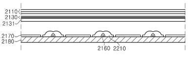
- the display device includes a display panel 2110, a backlight unit BLU1 that provides light to the display panel 2110, and a panel guide 2100 that supports a lower edge of the display panel 2110.
- the display panel 2110 is not particularly limited and may be, for example, a liquid crystal display panel including a liquid crystal layer.
- a gate driving PCB for supplying a driving signal to the gate line may be further located at the edge of the display panel 2110.
- the gate driving PCBs 2112 and 2113 may be formed on the thin film transistor substrate without being configured in a separate PCB.
- the backlight unit BLU1 includes a light source module including at least one substrate 2150 and a plurality of light emitting diode packages 2160.
- the backlight unit BLU1 may further include a bottom cover 2180, a reflective sheet 2170, a diffusion plate 2131, and optical sheets 2130.
- the bottom cover 2180 may be opened upward to accommodate the substrate 2150, the LED package 2160, the reflective sheet 2170, the diffusion plate 2131, and the optical sheets 2130.
- the bottom cover 2180 may be combined with the panel guide 2100.
- the substrate 2150 may be disposed under the reflective sheet 2170 and may be disposed in a form surrounded by the reflective sheet 2170.
- the present invention is not limited thereto, and when the reflective material is coated on the surface, the reflective material may be positioned on the reflective sheet 2170.
- the substrate 2150 may be formed in plural, and the plurality of substrates 2150 may be arranged side by side, but the present invention is not limited thereto and may be formed of a single substrate 2150.
- the LED package 2160 may include at least one of the LED packages according to the above-described embodiments of the present invention.
- the light emitting diode packages 2160 may be regularly arranged on the substrate 2150 in a predetermined pattern.
- a lens 2210 may be disposed on each LED package 2160 to improve uniformity of light emitted from the plurality of LED packages 2160.
- the diffusion plate 2131 and the optical sheets 2130 are positioned on the light emitting diode package 2160. Light emitted from the LED package 2160 may be supplied to the display panel 2110 in the form of a surface light source through the diffusion plate 2131 and the optical sheets 2130.
- the LED package manufactured according to the LED package manufacturing method according to the embodiments of the present invention may be applied to the direct type display device as in the present embodiment.
- FIG. 24 is a cross-sectional view for describing an example of applying the LED package to the display device using the LED package manufacturing method according to an embodiment.
- the display device including the backlight unit includes a display panel 3210 on which an image is displayed and a backlight unit BLU2 disposed on a rear surface of the display panel 3210 to irradiate light.
- the display device includes a frame 240 that supports the display panel 3210 and accommodates the backlight unit BLU2, and covers 3240 and 3280 that surround the display panel 3210.
- the display panel 3210 is not particularly limited and may be, for example, a liquid crystal display panel including a liquid crystal layer.
- a gate driving PCB for supplying a driving signal to the gate line may be further located at an edge of the display panel 3210.
- the gate driving PCB is not configured in a separate PCB, but may be formed on the thin film transistor substrate.
- the display panel 3210 may be fixed by covers 3240 and 3280 positioned at upper and lower portions thereof, and the cover 3280 positioned at lower portions thereof may be coupled to the backlight unit BLU2.
- the backlight unit BLU2 that provides light to the display panel 3210 is positioned in parallel with the light source module disposed on one side of the lower cover 3270, a portion of the lower cover 3270, and the light source module. And a light guide plate 3250 for converting point light into surface light.
- the backlight unit BLU2 according to the present exemplary embodiment is disposed on the light guide plate 3250 and is disposed below the light guide plate 3250 and the optical sheets 3230 for diffusing and condensing light.
- a reflective sheet 3260 may be further included to reflect the light toward the display panel 3210.
- the light source module includes a substrate 3220 and a plurality of light emitting diode packages 3110 spaced at regular intervals from one surface of the substrate 3220.
- the substrate 3220 is not limited as long as it supports the LED package 3110 and is electrically connected to the LED package 3110.
- the substrate 3220 may be a printed circuit board.
- the light emitting diode package 3110 may include at least one light emitting diode package according to the above-described embodiments of the present invention.
- Light emitted from the light source module is incident to the light guide plate 3250 and is supplied to the display panel 3210 through the optical sheets 3230. Through the light guide plate 3250 and the optical sheets 3230, the point light sources emitted from the light emitting diode packages 3110 may be transformed into surface light sources.
- the LED package according to the LED package manufacturing method according to the embodiments of the present invention can be applied to the edge type display device as in the present embodiment.
- 25 is a cross-sectional view illustrating an example in which a light emitting diode package according to a method of manufacturing a light emitting diode package according to an embodiment of the present invention is applied to a head lamp.
- the head lamp includes a lamp body 4070, a substrate 4020, a light emitting diode package 4010, and a cover lens 4050. Furthermore, the head lamp may further include a heat dissipation unit 4030, a support rack 4060, and a connection member 4040.
- the substrate 4020 is fixed by the support rack 4060 and spaced apart from the lamp body 4070.
- the substrate 4020 is not limited as long as it is a substrate capable of supporting the light emitting diode package 4010.
- the substrate 4020 may be a substrate having a conductive pattern such as a printed circuit board.
- the light emitting diode package 4010 is positioned on the substrate 4020 and may be supported and fixed by the substrate 4020.
- the LED package 4010 may be electrically connected to an external power source through the conductive pattern of the substrate 4020.
- the LED package 4010 may include at least one LED package according to the above-described embodiments of the present invention.
- the cover lens 4050 is positioned on a path along which light emitted from the LED package 4010 travels.
- the cover lens 4050 may be disposed spaced apart from the light emitting diode package 4010 by the connecting member 4040, and in a direction to provide light emitted from the light emitting diode package 4010. Can be arranged.
- the connection member 4040 may fix the cover lens 4050 with the substrate 4020 and may be disposed to surround the light emitting diode package 4010 to serve as a light guide for providing the light emitting path 4045. .
- connection member 4040 may be formed of a light reflective material or coated with a light reflective material.
- the heat dissipation unit 4030 may include a heat dissipation fin 4031 and / or a heat dissipation fan 4033, and radiate heat generated when the LED package 4010 is driven to the outside.
- the LED package according to the LED package manufacturing method according to the embodiments of the present invention may be applied to the head lamp, in particular, a vehicle head lamp.
Landscapes
- Led Device Packages (AREA)
Abstract
Un procédé de fabrication d'un boîtier de diodes électroluminescentes consiste à: placer une première brasure et une seconde brasure entre un substrat et une diode électroluminescente; et soumettre la première brasure et la seconde brasure à un traitement thermique pour fixer le substrat et la diode électroluminescente, le traitement thermique des première et seconde brasures comprenant: une étape de chauffage pour augmenter la température des première et seconde brasures de la température ambiante à une température Tp ; une étape de maintient pour maintenir la température Tp ; et une étape de refroidissement pour abaisser la température Tp ; l'étape de chauffage comprenant : une première étape d'augmentation pour faire passer une température de la température ambiante à une température TA à une vitesse constante ; une étape de préchauffage pour augmenter la température de la température TA à une température TB afin de conférer une fluidité aux première et seconde brasures ; et une seconde étape d'augmentation pour faire passer la température de TB à TL à une vitesse constante, l'étape de préchauffage étant effectuée sur 60 secondes à 180 secondes.
Priority Applications (1)
| Application Number | Priority Date | Filing Date | Title |
|---|---|---|---|
| US15/868,976 US10593850B2 (en) | 2015-07-15 | 2018-01-11 | Method for manufacturing light emitting diode package |
Applications Claiming Priority (4)
| Application Number | Priority Date | Filing Date | Title |
|---|---|---|---|
| KR20150100671 | 2015-07-15 | ||
| KR10-2015-0100671 | 2015-07-15 | ||
| KR1020160087556A KR20170009750A (ko) | 2015-07-15 | 2016-07-11 | 발광 다이오드 패키지 제조 방법 |
| KR10-2016-0087556 | 2016-07-11 |
Related Child Applications (1)
| Application Number | Title | Priority Date | Filing Date |
|---|---|---|---|
| US15/868,976 Continuation US10593850B2 (en) | 2015-07-15 | 2018-01-11 | Method for manufacturing light emitting diode package |
Publications (1)
| Publication Number | Publication Date |
|---|---|
| WO2017010818A1 true WO2017010818A1 (fr) | 2017-01-19 |
Family
ID=57757997
Family Applications (1)
| Application Number | Title | Priority Date | Filing Date |
|---|---|---|---|
| PCT/KR2016/007645 Ceased WO2017010818A1 (fr) | 2015-07-15 | 2016-07-14 | Procédé de fabrication de boîtier de diodes électroluminescentes |
Country Status (1)
| Country | Link |
|---|---|
| WO (1) | WO2017010818A1 (fr) |
Cited By (1)
| Publication number | Priority date | Publication date | Assignee | Title |
|---|---|---|---|---|
| US12464878B2 (en) * | 2022-04-22 | 2025-11-04 | Seoul Viosys Co., Ltd. | Light emitting module and display device including the same |
Citations (5)
| Publication number | Priority date | Publication date | Assignee | Title |
|---|---|---|---|---|
| JP2003338640A (ja) * | 2002-05-21 | 2003-11-28 | Rohm Co Ltd | 半導体チップを使用した半導体装置 |
| JP4141549B2 (ja) * | 1997-11-07 | 2008-08-27 | シャープ株式会社 | 半導体発光装置の製造方法 |
| JP2009004716A (ja) * | 2007-06-25 | 2009-01-08 | Mitsubishi Chemicals Corp | Led装置の製造方法 |
| KR20120048330A (ko) * | 2010-11-05 | 2012-05-15 | 서울옵토디바이스주식회사 | 발광 다이오드 어셈블리 및 그의 제조 방법 |
| JP2014067782A (ja) * | 2012-09-25 | 2014-04-17 | Toyoda Gosei Co Ltd | Ledチップの実装方法 |
-
2016
- 2016-07-14 WO PCT/KR2016/007645 patent/WO2017010818A1/fr not_active Ceased
Patent Citations (5)
| Publication number | Priority date | Publication date | Assignee | Title |
|---|---|---|---|---|
| JP4141549B2 (ja) * | 1997-11-07 | 2008-08-27 | シャープ株式会社 | 半導体発光装置の製造方法 |
| JP2003338640A (ja) * | 2002-05-21 | 2003-11-28 | Rohm Co Ltd | 半導体チップを使用した半導体装置 |
| JP2009004716A (ja) * | 2007-06-25 | 2009-01-08 | Mitsubishi Chemicals Corp | Led装置の製造方法 |
| KR20120048330A (ko) * | 2010-11-05 | 2012-05-15 | 서울옵토디바이스주식회사 | 발광 다이오드 어셈블리 및 그의 제조 방법 |
| JP2014067782A (ja) * | 2012-09-25 | 2014-04-17 | Toyoda Gosei Co Ltd | Ledチップの実装方法 |
Cited By (1)
| Publication number | Priority date | Publication date | Assignee | Title |
|---|---|---|---|---|
| US12464878B2 (en) * | 2022-04-22 | 2025-11-04 | Seoul Viosys Co., Ltd. | Light emitting module and display device including the same |
Similar Documents
| Publication | Publication Date | Title |
|---|---|---|
| US7683539B2 (en) | Light emitting device package and method for manufacturing the same | |
| WO2014069880A1 (fr) | Lentille et module d'émission de lumière pour éclairage par la surface | |
| WO2016148424A1 (fr) | Élément d'émission de lumière comprenant un substrat métallique | |
| WO2021085935A1 (fr) | Élément électroluminescent pour affichage et appareil d'affichage le comportant | |
| WO2021086026A1 (fr) | Dispositif d'affichage à del | |
| WO2016204482A1 (fr) | Élément électroluminescent comportant une pluralité d'unités de conversion de longueur d'onde, et procédé de fabrication de cet élément | |
| WO2020036423A1 (fr) | Dispositif électroluminescent | |
| WO2015190722A1 (fr) | Élément électroluminescent et dispositif d'éclairage | |
| WO2021054702A1 (fr) | Élément électroluminescent pour affichage, et boîtier électroluminescent le comprenant | |
| WO2014182104A1 (fr) | Module de source lumineuse et unité de rétroéclairage dotée de celui-ci | |
| WO2015064883A1 (fr) | Module de source de lumière et unité de rétroéclairage dotée de celui-ci | |
| WO2019027192A1 (fr) | Boîtier de dispositif à semi-conducteur et dispositif de source de lumière | |
| WO2017010701A1 (fr) | Diode électroluminescente comprenant une électrode transparente zno | |
| WO2021080311A1 (fr) | Dispositif d'affichage à del | |
| WO2013024916A1 (fr) | Puce de conversion de longueur d'onde pour une diode électroluminescente, et son procédé de fabrication | |
| WO2021085993A1 (fr) | Dispositif électroluminescent pour affichage, et appareil d'affichage à del le comprenant | |
| KR102478524B1 (ko) | 고효율 발광 다이오드 | |
| WO2014035087A1 (fr) | Module électroluminescent destiné à l'éclairage d'une surface | |
| WO2016186330A1 (fr) | Élément électroluminescent | |
| WO2020241993A1 (fr) | Diode électroluminescente verticale | |
| WO2022186634A1 (fr) | Carte de circuit imprimé ayant de multiples réserves de soudure et dispositif d'affichage la comprenant | |
| WO2017010818A1 (fr) | Procédé de fabrication de boîtier de diodes électroluminescentes | |
| WO2022055314A1 (fr) | Unité de pixel ayant des éléments électroluminescents et appareil d'affichage | |
| US10593850B2 (en) | Method for manufacturing light emitting diode package | |
| KR102475409B1 (ko) | 금속 벌크를 포함하는 발광 소자 |
Legal Events
| Date | Code | Title | Description |
|---|---|---|---|
| 121 | Ep: the epo has been informed by wipo that ep was designated in this application |
Ref document number: 16824735 Country of ref document: EP Kind code of ref document: A1 |
|
| NENP | Non-entry into the national phase |
Ref country code: DE |
|
| 122 | Ep: pct application non-entry in european phase |
Ref document number: 16824735 Country of ref document: EP Kind code of ref document: A1 |