WO2017014094A1 - 窒化物半導体発光素子 - Google Patents
窒化物半導体発光素子 Download PDFInfo
- Publication number
- WO2017014094A1 WO2017014094A1 PCT/JP2016/070451 JP2016070451W WO2017014094A1 WO 2017014094 A1 WO2017014094 A1 WO 2017014094A1 JP 2016070451 W JP2016070451 W JP 2016070451W WO 2017014094 A1 WO2017014094 A1 WO 2017014094A1
- Authority
- WO
- WIPO (PCT)
- Prior art keywords
- layer
- electrode
- mesa
- metal layer
- nitride semiconductor
- Prior art date
- Legal status (The legal status is an assumption and is not a legal conclusion. Google has not performed a legal analysis and makes no representation as to the accuracy of the status listed.)
- Ceased
Links
Images







Classifications
-
- H—ELECTRICITY
- H10—SEMICONDUCTOR DEVICES; ELECTRIC SOLID-STATE DEVICES NOT OTHERWISE PROVIDED FOR
- H10H—INORGANIC LIGHT-EMITTING SEMICONDUCTOR DEVICES HAVING POTENTIAL BARRIERS
- H10H20/00—Individual inorganic light-emitting semiconductor devices having potential barriers, e.g. light-emitting diodes [LED]
- H10H20/80—Constructional details
- H10H20/81—Bodies
- H10H20/822—Materials of the light-emitting regions
- H10H20/824—Materials of the light-emitting regions comprising only Group III-V materials, e.g. GaP
- H10H20/825—Materials of the light-emitting regions comprising only Group III-V materials, e.g. GaP containing nitrogen, e.g. GaN
-
- H—ELECTRICITY
- H10—SEMICONDUCTOR DEVICES; ELECTRIC SOLID-STATE DEVICES NOT OTHERWISE PROVIDED FOR
- H10H—INORGANIC LIGHT-EMITTING SEMICONDUCTOR DEVICES HAVING POTENTIAL BARRIERS
- H10H20/00—Individual inorganic light-emitting semiconductor devices having potential barriers, e.g. light-emitting diodes [LED]
- H10H20/80—Constructional details
- H10H20/83—Electrodes
-
- H—ELECTRICITY
- H10—SEMICONDUCTOR DEVICES; ELECTRIC SOLID-STATE DEVICES NOT OTHERWISE PROVIDED FOR
- H10H—INORGANIC LIGHT-EMITTING SEMICONDUCTOR DEVICES HAVING POTENTIAL BARRIERS
- H10H20/00—Individual inorganic light-emitting semiconductor devices having potential barriers, e.g. light-emitting diodes [LED]
- H10H20/80—Constructional details
- H10H20/83—Electrodes
- H10H20/831—Electrodes characterised by their shape
-
- H—ELECTRICITY
- H10—SEMICONDUCTOR DEVICES; ELECTRIC SOLID-STATE DEVICES NOT OTHERWISE PROVIDED FOR
- H10H—INORGANIC LIGHT-EMITTING SEMICONDUCTOR DEVICES HAVING POTENTIAL BARRIERS
- H10H20/00—Individual inorganic light-emitting semiconductor devices having potential barriers, e.g. light-emitting diodes [LED]
- H10H20/80—Constructional details
- H10H20/83—Electrodes
- H10H20/832—Electrodes characterised by their material
Definitions
- the present invention relates to a group III nitride semiconductor light emitting device having an emission peak wavelength of ultraviolet rays.
- the present invention relates to a technique for suppressing a decrease in light emission efficiency of an element due to current concentration at a mesa structure end of the light emitting element.
- the present invention also relates to a wafer including the light emitting device configuration.
- FIG. 8A and 8B show a typical schematic structure of the group III nitride semiconductor light emitting device 41.
- FIG. 8A is a top view of the element
- FIG. 8B is a cross-sectional view taken along line AA of FIG. 8A.
- the group III nitride semiconductor light emitting device 41 includes a stacked body including an n-type layer 12, an active layer 13, and a p-type layer 14 on one surface side of the substrate 11 (hereinafter sometimes referred to as “laminated semiconductor layer”). And a mesa structure 15 formed in a part of the laminated semiconductor layer is known.
- the mesa structure 15 is formed by forming a laminated semiconductor layer including the n-type layer 12, the active layer 13, and the p-type layer 14 on one surface side of the substrate 11, and then removing a part of the laminated structure by etching or the like. A part of 12 is exposed.
- a mesa structure 15 is formed by leaving a plateau-like portion (also referred to as a mesa) including the active layer 13 and the p-type layer 14 (see Patent Document 1).
- An n-electrode 16 is formed on the exposed surface of the n-type layer 12, and a p-electrode 17 is formed on the surface of the p-type layer 14.
- the current flows between the p electrode and the n electrode. Since the current tends to flow through a low resistance path (usually the shortest path), the current is in the vicinity of the end of the mesa structure 15 (hereinafter sometimes referred to as “mesa end”) close to the n electrode and the p electrode. Concentrate on the flow. As a result, the current does not flow uniformly in the active layer 13 and uneven light emission occurs, resulting in a decrease in light emission efficiency.
- Patent Document 2 discloses an ultraviolet semiconductor in which a p-type layer or a high-resistance layer having a higher resistance than a p-electrode is formed on the surface of the p-type layer on the side close to the n-electrode along the shape of the p-type layer side. A light emitting device is disclosed.
- a high resistance layer is formed on a p-type layer near the mesa edge as in Patent Document 2, it is possible to suppress current concentration in a region near the mesa edge.
- Patent Document 3 discloses a semiconductor light emitting device in which a trench is formed between a p electrode and an n electrode. By forming the trench, the variation in the length of the current path flowing between the p electrode and the n electrode is reduced, and the current is prevented from concentrating on a specific portion. However, in order to sufficiently reduce the variation in the length of the current path, it is necessary to increase the depth of the trench.
- the n-type layer has a high Al composition, so that the specific resistance of the n-type layer is increased and current is concentrated in a region near the mesa edge. Almost flow, and it tends to cause a decrease in luminous efficiency. Therefore, it has been desired to develop a light emitting element that can suppress a decrease in light emission efficiency due to current concentration.
- the present invention provides a technique for suppressing a decrease in luminous efficiency by suppressing a current flowing between a p-electrode and an n-electrode from being concentrated in a region near the mesa edge in a semiconductor element having a mesa structure.
- the purpose is that.
- the present inventor thought that the above problem could be solved by adjusting the structure of the p-electrode, and conducted intensive studies.
- the group III nitride semiconductor device has a p-electrode (hereinafter sometimes referred to as “p-type electrode structure 30”) in which a first metal layer, a conductive layer, and a second metal layer are laminated in this order. And it discovered that the said subject could be solved by making the specific resistance of the said conductive layer higher than the specific resistance of the said 1st metal layer, and came to complete this invention.
- the first invention is a group III nitride semiconductor device including an active layer between an n-type layer and a p-type layer and having a mesa structure including the p-type layer, and is on the n-type layer.
- It is a group III nitride semiconductor device having a higher specific resistance.
- the thickness of the conductive layer is 0.05 ⁇ m or more and 20 ⁇ m or less, and the specific resistance of the conductive layer is 0.1 ⁇ 10 ⁇ 4 to 1.0 ⁇ 10 ⁇ 2. It is a group III nitride semiconductor device having ⁇ cm.
- a third invention is a group III according to the first or second invention, wherein the first metal layer is a layer in ohmic contact with the p-type layer, and is composed of a single metal or two or more metals. It is a nitride semiconductor device.
- the distance between the mesa end of the group III nitride semiconductor device and the outer periphery of the second metal layer is not less than 1/3 of the diffusion length L s. It is a certain group III nitride semiconductor device.
- the distance between at least the protrusion at the mesa end and the outer periphery of the second metal layer in the top view of the group III nitride semiconductor device is equal to 1 of the diffusion length L s .
- This is a group III nitride semiconductor device that is / 3 or more.
- a sixth invention provides a group III nitride semiconductor device according to the first to third inventions, wherein the distance between the mesa end of the group III nitride semiconductor device and the outer periphery of the second metal layer is 20 ⁇ m or more. It is.
- a seventh invention is the group III according to the first to third inventions, wherein the distance between at least the protrusion of the mesa end and the outer periphery of the second metal layer in the top view of the group III nitride semiconductor device is 20 ⁇ m or more. It is a nitride semiconductor device.
- the eighth invention is a group III nitride semiconductor light emitting device according to the first to seventh inventions, wherein the emission peak wavelength is 200 to 350 nm.
- a group III nitride semiconductor light emitting device having an emission peak wavelength of 200 to 350 nm has a high Al composition in the n-type layer, so that the specific resistance of the n-type layer increases, current concentration at the mesa edge tends to occur, and the luminous efficiency is improved. It tends to cause a decline. Therefore, the configuration of the present invention is suitable.
- a ninth invention is a wafer comprising a group III nitride semiconductor device having a mesa structure including an active layer between an n-type layer and a p-type layer and having the p-type layer, the group III
- the nitride semiconductor device is a wafer according to the first to seventh aspects of the invention.
- a tenth invention is a wafer including a configuration of a group III nitride semiconductor light emitting device having an mesa structure including an active layer between an n-type layer and a p-type layer, and including the p-type layer,
- the group nitride semiconductor light emitting device is a wafer according to the configuration of the eighth invention.
- the group III nitride semiconductor element has a p-electrode formed by laminating a first metal layer, a conductive layer, and a second metal layer in this order on a p-type layer.
- the resistance higher than the specific resistance of the first metal layer, the current flowing between the p electrode and the n electrode is prevented from being concentrated in the region near the mesa end.
- a group III nitride semiconductor light-emitting device in which current easily flows uniformly through the active layer, light emission unevenness is suppressed, and reduction in light emission efficiency is suppressed can be obtained.
- the first metal layer and the conductive layer are formed on the entire laminated surface of the mesa portion.
- the distance between the mesa end and the outer periphery of the second metal layer can be set to a predetermined value or more.
- the distance between the mesa end and the outer periphery of the second metal layer can be set to a predetermined value or more at all the mesa ends.
- the distance between a part of the mesa edge and the outer periphery of the second metal layer can be set to a predetermined value or more. If the distance between the mesa end and the outer periphery of the second metal layer is greater than or equal to a predetermined value at all the mesa ends, the area of the second metal layer is reduced, and the resistance of the current flowing between the p electrode and the n electrode The value may increase and the operating voltage may increase.
- the second metal layer can be formed widely, and the resistance of the current flowing between the p electrode and the n electrode It is possible to suppress an increase in value and suppress an increase in operating voltage.
- the distance between at least the protrusion at the mesa end and the outer periphery of the second metal layer can be set to a predetermined value or more.
- a predetermined value or more By increasing the distance between at least the protrusion of the mesa end and the outer periphery of the second metal layer to a predetermined value or more, an increase in operating voltage is suppressed, and the current flowing between the p electrode and the n electrode is near the mesa end. Concentration can be suppressed. As a result, the decrease in luminous efficiency is further suppressed, and the occurrence of quality defects can be reduced.
- an ultraviolet light-emitting element having an emission peak wavelength in the range of 200 to 350 nm has a higher Al composition than that of a light-emitting element having an emission peak wavelength exceeding 350 nm, for example, a light-emitting element in the visible light region.
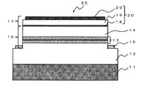
- FIG. 1 is a cross-sectional view of a group III nitride semiconductor device of the present invention.
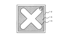
- An example of a group III nitride semiconductor device viewed from above is shown.
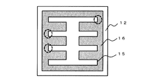
- An example of a group III nitride semiconductor device viewed from above is shown.
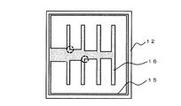
- An example of a group III nitride semiconductor device viewed from above is shown.
- An example of a group III nitride semiconductor device viewed from above is shown.
- An example of a group III nitride semiconductor device viewed from above is shown.
- An example of a group III nitride semiconductor device viewed from above is shown.
- An example of a group III nitride semiconductor device viewed from above is shown.
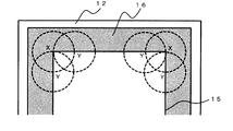
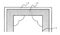
- a method for determining a “mesa edge protrusion” using a definition circle is shown. Various mesa end shapes are shown. A method for determining the second metal layer restriction region will be described. A method for determining the second metal layer restriction region will be described. The positional relationship between the mesa end of the element and the second metal layer is shown. The example of the positional relationship of a mesa edge and a 2nd metal layer is shown. The example of the positional relationship of a mesa edge and a 2nd metal layer is shown.
- An example of a typical group III nitride semiconductor light emitting device viewed from above is shown. 1 shows a cross-sectional view of a typical group III nitride semiconductor light emitting device. 3 shows a group III nitride semiconductor light-emitting device viewed from the top in Examples 1 to 3. FIG. 3 shows a group III nitride semiconductor light-emitting device viewed from above in Example 4.
- FIG. 1 shows a cross-sectional view of
- the light emitting region of light emitted from the group III nitride semiconductor light emitting device of the present invention is not particularly limited. According to the present invention, it is possible to suppress a decrease in light emission efficiency due to local current concentration in the mesa structure regardless of the light emission region.
- the present invention is applied to a group III nitride semiconductor light emitting device having an emission peak wavelength in the visible light region or the ultraviolet region. More preferably, the present invention is applied to a group III nitride semiconductor light emitting device that emits ultraviolet light having an emission peak wavelength of 200 to 350 nm.
- a group III nitride semiconductor light emitting device having an emission peak wavelength of 200 to 350 nm will be mainly described.
- a group III nitride semiconductor device 40 of the present invention includes a substrate 11, a mesa structure 15 (laminated semiconductor layer) including an n-type layer 12, an active layer 13 and a p-type layer 14, an n-electrode, 16 and a p-electrode 17.
- the p-type electrode structure 30 constituting the p-electrode 17 includes a first metal layer 18, a conductive layer 19, and a second metal layer 20. In the following, non-limiting examples of these will be described.
- the “mesa edge” is the outline of the mesa structure 15, which is the edge of the mesa structure in a top view, and is shown as the outer periphery (that is, the outline) of the p-type layer 14.
- the mesa structure is formed by etching the stacked semiconductor layer substantially vertically, but does not have to be completely vertical, and may be formed in a tapered shape from the top to the bottom of the mesa structure.
- the taper part is observed in a top view.
- the taper part is formed in an overhang shape, so that it is difficult to observe the top view.
- the mesa end is the end of the mesa structure 15 in a top view, and is defined as the outer periphery (that is, the contour) of the p-type layer 14 positioned at the uppermost layer of the mesa structure, and does not include the taper portion.
- the refractive index, the transmittance and the reflectance were based on light having a wavelength of 265 nm. This is because light of wavelength 265 nm is most suitable for sterilization because DNA has maximum absorption in the vicinity of wavelength 265 nm, and is considered to have high industrial utility value.
- the refractive index, the transmittance, and the reflectance are simply used, the values are for light with a wavelength of 265 nm.
- the substrate 11 is not particularly limited as long as it can epitaxially grow a group III nitride semiconductor crystal on the surface and transmits ultraviolet rays.
- Examples of the material used for the substrate 11 include sapphire, SiC (silicon carbide), AlN (aluminum nitride), Si (silicon), and the like. Among them, an AlN single crystal substrate having a c-plane as a main surface is preferable.
- the transmittance of the substrate 11 with respect to light having a wavelength of 265 nm is preferably as high as possible, preferably 50% or more, and more preferably 60% or more.
- the upper limit of the transmittance of the substrate 11 is preferably 100%, but the upper limit is 80% in consideration of industrial production.
- the transmittance of the substrate can be adjusted by the material, substrate thickness, crystallinity, and impurity content.
- the thickness of the substrate 11 is not particularly limited, but is preferably 30 to 1500 ⁇ m, more preferably 50 to 1000 ⁇ m. By setting the thickness of the substrate 11 in the above range, the transmittance is improved and the productivity is improved.
- the thickness of the substrate 11 only needs to satisfy the above range after the manufacture of the group III nitride semiconductor element, and the thickness of the substrate is obtained by grinding or polishing the lower surface of the substrate after laminating a laminated semiconductor layer and electrodes described later on the substrate. May be in the above range.
- the laminated semiconductor layer (the main part of the device including the mesa structure 15 in FIG. 1) is formed on the substrate 11 as shown in FIG. 1, and the n-type layer 12, the active layer 13, and the p-type layer 14 (p-type cladding layer). And a layer made of a p-type contact layer) are laminated in this order. Non-limiting examples are described below for each layer.
- Group III nitride semiconductor preferably containing impurities.
- the impurity concentration is 1.0 ⁇ 10 17 cm ⁇ 3 or more and 5.0 ⁇ 10 20 cm ⁇ 3 or less, preferably 1.0 ⁇ 10 18 cm ⁇ 3 or more and 5.0 ⁇ 10 19 cm ⁇ 3 or less.
- the refractive index of the n-type layer is not particularly limited, but is 1.5 to 3.0.
- the refractive index may be adjusted by the composition of the n-type layer.
- the thickness of the n-type layer is 100 nm or more and 10,000 nm or less, preferably 500 nm or more and 3000 nm or less.
- the group III nitride semiconductor device 40 includes a group III having the same or similar composition as AlN or the n-type layer between the substrate 11 and the n-type layer 12.
- a buffer layer including a nitride semiconductor may be included.
- a well layer having a band gap energy larger than that of the well layer (x, y, z are 0 ⁇ x ⁇ 1.0, 0 ⁇ y ⁇ 0.1, 0 ⁇ z ⁇ 1.0).
- the active layer may be a multiple quantum well structure or a single quantum well structure.
- the thickness of the well layer is 1 nm or more, preferably 2 nm or more, and the upper limit is 100 nm.
- the thickness of the barrier layer is 1 nm or more, preferably 2 nm or more, and the upper limit is 1 ⁇ m.
- Such an active layer can be manufactured by the MOCVD method.
- the p-type layer 14 includes a p-type cladding layer and a p-type contact layer.
- Group III nitride semiconductor preferably containing impurities.
- the impurity of the p-type cladding layer is preferably Mg.
- the impurity concentration in the p-type cladding layer is 1.0 ⁇ 10 17 cm ⁇ 3 or more and 5.0 ⁇ 10 20 cm ⁇ 3 or less, preferably 1.0 ⁇ 10 18 cm ⁇ 3 or more and 5.0 ⁇ 10 20 cm ⁇ . 3 or less.
- the thickness of the p-type cladding layer is 5 nm to 100 nm, preferably 10 nm to 80 nm.
- the p-type contact layer is made of GaN. If the p-type contact layer is made of GaN, that is, a p-GaN layer, the contact characteristics of the p-type contact layer can be improved.
- the p-type contact layer preferably contains an impurity.
- the impurity of the p-type contact layer is preferably Mg, like the p-type cladding layer.
- the impurity concentration in the p-type contact layer is 1.0 ⁇ 10 17 cm ⁇ 3 or more and 5.0 ⁇ 10 20 cm ⁇ 3 or less, preferably 1.0 ⁇ 10 18 cm ⁇ 3 or more and 2.0 ⁇ 10 20 cm ⁇ . 3 or less.
- the thickness of the p-type contact layer is 1 nm to 200 nm, preferably 5 nm to 50 nm. By setting the thickness of the p-type contact layer within the above range, the contact characteristics of the p-type layer are improved.
- the n electrode 16 is formed on the exposed surface of the n-type layer 12.
- the exposed surface of the n-type layer is formed by means such as etching.
- the stacked semiconductor layer remains in a plateau shape, and the mesa structure 15 is formed.
- the n-electrode on the n-type layer is formed along the lower end of the mesa structure in the low-level portion of the mesa structure, but is slightly spaced from the bottom of the mesa structure and is n-type between the mesa structure 15 and the n-electrode 16.
- the structure in which the layer 12 is exposed may be used.
- the n electrode 16 may be formed so as to surround the entire p electrode 17 along the mesa edge, and the n electrode may be formed so as to surround a part of the p electrode. May be.
- the p electrode may be formed so as to surround the n electrode.
- Etching techniques include dry etching such as reactive ion etching and inductively coupled plasma etching.
- the exposed surface is preferably surface-treated with an acid or alkali solution in order to remove etching damage.
- an n-type electrode 16 having ohmic properties is formed on the exposed surface of the n-type layer.
- the patterning of the n electrode can be performed using a lift-off method.
- a photoresist is applied to the surface on which the electrode is to be formed, irradiated with ultraviolet rays using a UV exposure machine equipped with a photomask, and immersed in a developer to dissolve the exposed photoresist to form a desired pattern.
- an electrode metal is deposited on the patterned photoresist, and the photoresist is dissolved with a stripping solution to form an electrode metal pattern.
- an electrode metal film is formed on the electrode formation surface, a photoresist is applied, the photoresist is patterned through an exposure and development process, and the electrode is formed by dry etching or wet etching using the photoresist as a mask.
- a method of patterning a metal and dissolving the photoresist with a stripping solution is preferable because the process is relatively simple.
- Examples of the method for depositing the n-electrode metal include vacuum deposition, sputtering, and chemical vapor deposition. In particular, vacuum deposition is preferable because impurities in the electrode metal can be eliminated.
- the material used for the n-electrode can be selected from known materials. For example, Ti, Al, Rh, Cr, In, Ni, Pt, Au, etc. are mentioned. Among these, Ti, Al, Rh, Cr, Ni, and Au are preferable. In particular, a combination of Ti, Al, and Au is preferable because it can improve ohmic properties and reflectivity.
- the n-electrode may be a single layer containing an alloy or oxide of these metals, or a multilayer structure.
- the thickness of the n-electrode is not particularly limited, but is preferably 2 nm or more in consideration of production stability, and the upper limit is 2 ⁇ m.
- the pattern of the n electrode is not particularly limited, and may be formed so as to surround the entire mesa structure 15 along the mesa edge (FIGS. 2A to 2F). It may be formed so as to surround a part of the structure 15 (FIG. 2G). Further, the n electrode may be formed so as to surround the p electrode (FIGS. 2A to E and G), and conversely, the p electrode may be formed so as to surround the n electrode (FIG. 2F).
- the width of the n electrode is not particularly limited, but is usually about 5 to 100 ⁇ m, preferably 10 to 50 ⁇ m.
- the width of the n electrode may not be uniform. For example, a narrow part and a wide part may be mixed. In this case, the average width of the n electrodes may be in the above range.
- heat treatment is performed at a temperature of 300 ° C. to 1100 ° C. for 30 seconds to 3 minutes.
- optimal conditions can be selected suitably according to the metal seed
- the p-electrode 17 of the present invention has a p-type electrode structure 30.
- the first metal layer 18, the conductive layer 19, and the second metal layer 20 are laminated in this order.
- the p-type electrode structure 30 in which the p-electrode 17 of the group III nitride semiconductor element is formed by laminating the first metal layer 18, the conductive layer 19, and the second metal layer 20 in this order It has been found that by having it, current concentration can be suppressed and a decrease in luminous efficiency can be suppressed.
- the current is applied to the second metal layer 20 and the first metal layer 20 in the p-type electrode structure constituting the p-electrode.
- An attempt is made to flow along a path with low resistance to the metal layer 18. Since the conductive layer 19 immediately below the second metal layer 20 has a higher specific resistance than the first metal layer 18 immediately below the conductive layer, the current is conducted through the conductive layer through the shortest path, and the first metal layer 18 is passed through. The tendency to flow increases.
- the conductive layer 19 having a high specific resistance is interposed between the second metal layer 20 and the first metal layer 18, the current is suppressed from being concentrated in a region near the mesa edge. It is possible to flow through the laminated semiconductor layer without concentration.
- the operating voltage does not increase excessively.
- the specific resistance value of the conductive layer 19 becomes close to the specific resistance value of the n-type layer 12 by increasing the specific resistance of the conductive layer 19.
- the value of the diffusion length L s in the n-type layer 12 increases, the electron diffusion distance in the n-type layer increases, and current concentration in the vicinity of the mesa edge in the n-type layer is suppressed. That is, due to the conductive layer 19 having a high specific resistance, current flows to the active layer 13 without being concentrated locally, and a decrease in light emission efficiency is suppressed.
- the present invention local concentration of current in the p-type electrode structure 30 can be suppressed.
- the current flowing between the p-electrode 17 and the n-electrode 16 having the p-type electrode structure 30 is also prevented from being concentrated in a region near the mesa end, and a decrease in luminous efficiency can be suppressed.
- the first metal layer 18, the conductive layer 19, and the second metal layer 20 that form the p-type electrode structure 30 will be described below.
- the first metal layer 18 is formed so as to be in ohmic contact with the p-type layer 14.
- the metal material used for the first metal layer 18 is preferably Ni, Au, Pt, Pd, Ru, Os, Rh, Ir, or Ag, and more preferably Ni, Au, Pt, or Pd. From these, a material having a specific resistance lower than that of the material constituting the conductive layer 19 described in detail below may be selected. In the first metal layer, these metals may be used alone or in combination of two or more.
- the first metal layer 18 may be a single layer containing an alloy or oxide of these metals or a multilayer structure.
- Specific resistance of the first metal layer 18 is preferably 1 ⁇ 10 -6 ⁇ 2 ⁇ 10 -5 ⁇ cm, more preferably 1 ⁇ 10 -6 ⁇ 1 ⁇ 10 -5 ⁇ cm.
- the specific resistance of the first metal layer 18 is lower than the specific resistance of the conductive layer 19 described later.
- the thickness of the first metal layer 18 is preferably 1 nm or more and 200 nm or less, more preferably 2 nm or more and 100 nm or less from the viewpoint of productivity.
- the patterning of the first metal layer 18 is preferably performed using a lift-off method, as is the patterning of the n-electrode.
- the shape and size of the first metal layer 18 are substantially similar to the mesa structure 15.
- the first metal layer 18 may be formed in a similar shape slightly smaller than the mesa structure 15.
- the first metal layer 18 is formed on the entire laminated surface of the p-type layer.
- the first metal layer 18 As a method for depositing the first metal layer 18, for example, vacuum deposition, sputtering, chemical vapor deposition, and the like can be cited as in the method for forming the n-electrode.
- vacuum deposition is preferable because impurities in the electrode metal can be eliminated.
- heat-treat at a temperature of 200 ° C. to 800 ° C. for 30 seconds to 3 minutes after depositing the metal. About the temperature and time of heat processing, optimal conditions can be suitably selected according to the metal seed
- the conductive layer 19 is formed on the first metal layer.
- the material used for the conductive layer 19 is preferably ZnO, ZnO doped with Al (hereinafter simply referred to as AZO), SnO 2 doped with Sb (hereinafter simply referred to as ATO), or ZnO with Ge.
- Doped hereinafter simply referred to as GZO
- oxide conductors are Ge, Si, and Ti, and more preferably ZnO, AZO, ITO, ATO, GZO, Ge, Si, and Ti.
- the specific resistance of the conductive layer 19 is preferably 0.1 ⁇ 10 ⁇ 4 to 1.0 ⁇ 10 ⁇ 2 ⁇ cm, more preferably 0.5 ⁇ 10 ⁇ 4 to 1.0 ⁇ 10 ⁇ 2 ⁇ cm. .
- the specific resistance of the conductive layer 19 is higher than the specific resistance of the first metal layer 18.
- the conductive layer 19 In the present invention, in order to suppress the current flowing in the conductive layer from being concentrated in a region near the mesa edge and to further suppress the excessive increase in the operating voltage, the conductive layer 19
- the specific resistance of the first metal layer 18 is preferably 2 to 1000 times, more preferably 4 to 1000 times, still more preferably 4 to 500 times, and more preferably 4 to 100 times. It is particularly preferable to do this.
- the thickness of the conductive layer 19 is preferably 0.05 ⁇ m or more and 20 ⁇ m or less, and more preferably 0.05 ⁇ m or more and 10 ⁇ m or less. If the thickness of the conductive layer is too large, the operating voltage may increase. If the thickness of the conductive layer is too small, it is difficult for the current to sufficiently spread within the conductive layer, and it may not be possible to effectively suppress the current from being concentrated in the region near the mesa edge.
- the shape and size of the conductive layer 19 are almost similar to the mesa structure 15.
- the conductive layer 19 may be formed in a similar shape slightly smaller than the mesa structure 15.
- the conductive layer 19 is formed on the entire surface of the first metal layer.
- the conductive layer is formed by vacuum deposition, sputtering, MBE, or the like.
- the second metal layer 20 is formed on the conductive layer.
- the metal material used for the second metal layer 20 is preferably Ti, Ni, Pt, Au, Mo, W, and more preferably Ti, Ni—, Pt, Au. In the second metal layer 20, these metals may be used alone or in combination of two or more. Further, the second metal layer 20 may be a single layer containing an alloy or oxide of these metals, or a multilayer structure.
- the specific resistance of the second metal layer 20 is not particularly limited. Usually, the specific resistance of metal is small compared to the specific resistance of the material used for the conductive layer. Among them, in order to exert an excellent effect, the specific resistance of the second metal layer 20 is preferably 1.0 ⁇ 10 ⁇ 6 ⁇ cm or more and 5.0 ⁇ 10 ⁇ 5 ⁇ cm or less, and 2.0 ⁇ 10 6 More preferably, it is ⁇ 6 ⁇ cm or more and 5.0 ⁇ 10 ⁇ 5 ⁇ cm or less.
- the thickness of the second metal layer 20 is preferably 0.05 ⁇ m or more and 10 ⁇ m or less, and more preferably 0.10 ⁇ m or more and 7 ⁇ m or less. If the thickness of the second metal layer is too large, the stress generated inside the second metal layer is increased, and the second metal layer may be easily peeled off. If the thickness of the second metal layer is too small, the heat dissipation is reduced, and solder may be easily diffused when used as a semiconductor element.
- the patterning of the second metal layer 20 is preferably carried out using a lift-off method, similarly to the patterning of the n-electrode.
- a method for depositing the second metal layer 20 as in the method for forming the n-electrode, for example, vacuum deposition, sputtering, chemical vapor deposition, or the like can be given.
- vacuum deposition is preferable because impurities in the electrode metal can be eliminated.
- the shape and size of the second metal layer 20 may be similar to the mesa structure 15 or may be completely different from the mesa structure.
- the formation position of the second metal layer 20 in the p-type electrode structure 30 can be set based on a predetermined guideline related to the shape of the mesa structure 15. Thereby, current concentration at the mesa end can be further suppressed.
- the shape of the second metal layer 20 is not particularly limited, but can be formed in a similar shape slightly smaller than the mesa structure 15.
- the shape of the second metal layer 20 is a rectangular shape substantially similar to the mesa structure 15 shown in FIG. 2A, a cross shape as shown in FIGS. 2B and 2C, and as shown in FIGS. 2D to 2G. It may be comb-shaped.
- the width of the second metal layer is not particularly limited, but in the shape similar to the mesa structure 15 shown in FIGS. 2B to 2G, it is usually about 5 to 100 ⁇ m, preferably 10 to 50 ⁇ m.
- the width of the second metal layer may not be uniform. For example, a narrow part and a wide part may be mixed. In this case, the average width of the second metal layer may be in the above range.
- the p-electrode 17 is substantially similar to the mesa structure 15 on the p-type layer 14 positioned on the top of the plate-like mesa structure 15. Formed.
- the n-electrode 16 is formed in a lower low area as viewed from the mesa structure 15.
- a path with low resistance is given priority, so that the current is likely to be concentrated in a region near the end of the mesa structure 15 at the shortest distance between the n-electrode and the p-electrode.
- the group III nitride semiconductor device 40 of the present invention has a p-electrode 17 formed by laminating a first metal layer 18, a conductive layer 19, and a second metal layer 20 in this order in order to suppress current concentration at the mesa end. Furthermore, in a preferred embodiment of the present invention, the first metal layer 18 and the conductive layer 19 are formed over the entire laminated surface of the mesa portion, and the formation of the second metal layer 20 is to suppress current concentration at the mesa edge. A certain distance or more can be provided between the mesa end and the second metal layer 20.
- the distance between the outer periphery of the mesa edge and the second metal layer 20 and 1/3 or more of the diffusion length L s be able to.
- the distance between the mesa end and the outer periphery of the second metal layer 20 is the length of the shortest path from the arbitrarily selected mesa end to the contour of the second metal layer 20 in a top view.
- the distance between the outer periphery of the mesa end second metal layer is preferably 1/3 or more diffusion length L s, more preferably 1/3 or more of the diffusion length L s , 1.2 times the diffusion length L s or less, more preferably 1/3 or more of the diffusion length L s, is less than 1.0 times the diffusion length L s.
- the distance between the outer periphery of the mesa edge and the second metal layer 20 in all of the mesa edge may be 1/3 or more of the diffusion length L s.
- the distance between the outer periphery of the mesa edge and the second metal layer in all the mesa edge is preferably set to 1/3 or more of the diffusion length L s, more preferably diffusion length L s 1/3 or more, 1.2 times the diffusion length L s or less, more preferably 1/3 or more of the diffusion length L s, is less than 1.0 times the diffusion length L s.
- the distance between the outer periphery of the part of the mesa end the second metal layer may be more than one-third of the diffusion length L s. If the distance between the mesa end and the outer periphery of the second metal layer is 1/3 or more of the diffusion length L s at all the mesa ends, the area of the second metal layer is reduced, and the p electrode 17 and the n electrode 16 There is a risk that the resistance value of the current flowing between the two increases and the operating voltage increases.
- the second metal layer can be formed widely, and the p electrode and the n electrode It is possible to suppress an increase in the resistance value of the current flowing between them and suppress an increase in operating voltage.
- the distance between the outer periphery of the part of the mesa end the second metal layer is preferably 1/3 or more diffusion length L s, more preferably diffusion length L s of 1 / 3 or more, 1.2 times the diffusion length L s or less, more preferably 1/3 or more of the diffusion length L s, is less than 1.0 times the diffusion length L s.
- the distance between the outer layer 20 may be 1/3 or more of the diffusion length L s.
- the portion where current concentration is likely to occur refers to a portion where the p-electrode 17 protrudes into the n-electrode formation region in a top view.
- the portion since the p-electrode 17 is surrounded by the n-electrode 16, current tends to concentrate. As a result, the portion emits light more strongly, but the load is large and the deterioration tends to occur.
- the portion where current is concentrated emits light strongly, the light emission is weakened in other portions, so that uneven light emission occurs and the light emission efficiency tends to decrease.
- the second metal layer 20 of the p-type electrode structure constituting the p-electrode is formed on the mesa structure 15 in a shape substantially similar to the mesa structure, at least the mesa structure 15 is in the n-electrode formation region. If the distance between the mesa end and the second metal layer 20 is a predetermined value or more in the protruding portion, that is, the mesa end protrusion described in detail later, the current flowing from the second metal layer 20 is applied to the end of the mesa structure. It can flow to the conductive layer directly below without concentrating.
- the mesa structure 15 is an n-electrode.
- the distance between the at least projection and the outer periphery of the second metal layer 20 of the mesa edge is preferably set to 1/3 or more of the diffusion length L s, more preferably the diffusion length L s of 1/3 or more, 1.2 times the diffusion length L s or less, more preferably 1/3 or more of the diffusion length L s, is less than 1.0 times the diffusion length L s.
- the outer periphery n electrode of the second metal layer is less than 1/3 of the diffusion length L s It may be close by distance.
- ⁇ c contact resistance between p electrode / p-type layer and n electrode / n-type layer
- ⁇ p specific resistance of p-type layer
- ⁇ n specific resistance of n-type layer
- t p p-type layer Thickness
- t n the thickness of the n-type layer.
- the contact resistance is measured by a TLM (Transfer Length Method) method.
- a p-electrode pattern having a donut-shaped second metal layer non-formation region is formed on the surface of the p-GaN layer by a method similar to the method for manufacturing a semiconductor element (distance between electrodes: 5, 10, 20, 40 , 60, 80, 100 ⁇ m).
- the resistance value at each inter-electrode distance is measured, and the contact resistance between the p-electrode / p-type layer and the n-electrode / n-type layer is calculated from the relationship between the inter-electrode distance and the resistance value.
- the specific resistance of the p-type layer (p-GaN layer, p-AlGaN layer) and n-type layer (n-AlGaN layer) is calculated by measuring the Hall effect for the obtained sample.
- the diffusion length L s is the distance at which most electrons can diffuse in the n-type layer from the end of the n electrode near the mesa end to the mesa end in consideration of the movement of electrons to the p electrode. Point to.
- the diffusion length L s does not depend on the width of the electrode, it becomes a guideline for device design for suppressing current concentration even when the element is downsized and the electrode is thinned.
- the group III nitride semiconductor element has a p-electrode 17 formed by laminating the first metal layer 18, the conductive layer 19, and the second metal layer 20 in this order, Furthermore, although the distance between the mesa end and the outer periphery of the second metal layer 20 can be set to 1/3 or more of the diffusion length L s , in the present technology of the present invention, the mesa end and the second metal layer 20 It is sufficient that the distance from the outer periphery is 20 ⁇ m or more.
- the distance between the mesa edge and the outer periphery of the second metal layer 20 is preferably 20 ⁇ m or more, more preferably 20 to 80 ⁇ m, and even more preferably. Is 20 to 40 ⁇ m. From the viewpoint of further suppressing current concentration, the distance between the mesa edge and the outer periphery of the second metal layer 20 is preferably 20 ⁇ m or more at all mesa edges, more preferably 20 to 80 ⁇ m, and even more preferably 20 to 20 ⁇ m. 40 ⁇ m.
- the distance between a part of the mesa edge and the outer periphery of the second metal layer 20 is preferably 20 ⁇ m or more, more preferably 20 to 80 ⁇ m, still more preferably 20 to 40 ⁇ m. It is. From the viewpoint of suppressing current concentration and further suppressing increase in operating voltage, the distance between at least the protrusion at the mesa end and the outer periphery of the second metal layer 20 is preferably 20 ⁇ m or more, and more preferably 20 to 80 ⁇ m, more preferably 20 to 40 ⁇ m. This distance is sufficient for the current (2015) device design.
- the distance between the mesa end and the outer periphery of the second metal layer 20 may not be 20 ⁇ m or more.
- a guideline diffusion length L s it is sufficient to set the distance between the outer periphery of the mesa edge and the second metal layer 20.
- the group III nitride semiconductor device has a p-electrode 17 formed by laminating a first metal layer 18, a conductive layer 19, and a second metal layer 20 in this order, Between the mesa end and the second metal layer 20, a second metal layer restriction region in which the formation of the second metal layer is restricted can be provided. That is, in the preferred embodiment of the present invention may be present a second metal layer restricted area of more than 1/3 of the width or 20 ⁇ m or wider, the diffusion length L s in the vicinity of the end portion of the mesa structure.
- the second metal layer restriction region can be provided in the vicinity of all mesa edges.
- current concentration can be further suppressed, current can easily flow to the active layer, and light emission unevenness is suppressed. The decrease can be suppressed.
- the second metal layer restriction region can be provided in the vicinity of a part of the mesa end. If the second metal layer limiting region is provided in the vicinity of all the mesa edges, the area of the second metal layer is reduced, the resistance of the current flowing between the p electrode and the n electrode is increased, and the operating voltage is increased. May be.
- the second metal layer limiting region in the vicinity of a part of the mesa end, the second metal layer can be formed widely, and the resistance value of the current flowing between the p electrode and the n electrode increases. And an increase in operating voltage can be suppressed.
- the second metal layer limiting region can be provided at least in the vicinity of the protrusion at the mesa end. That is, in the preferred embodiment of the present invention, at least projections of the mesa edge, the second metal of more than 1/3 of the width or 20 ⁇ m or more of the width of the diffusion length L s between the mesa edge and the second metal layer 20
- the layer limiting region By providing the layer limiting region, an increase in operating voltage can be suppressed, and further, current does not easily flow in this region, so that current concentration in the vicinity of this region can be suppressed.
- the “projection at the end of the mesa” refers to a portion where the outline of the mesa structure 15 projects into the n-electrode formation region in a top view.
- the second metal layer is formed in this portion, electrons from the n electrode surrounding the periphery are concentrated on the second metal layer formed in the portion, and the active layer portion immediately below the second metal layer has a strong light.
- the light emitted from other parts is weak, and uneven light emission is likely to occur.
- the laminated semiconductor layer immediately below the second metal layer in the portion is likely to deteriorate.
- FIG. 2 shows a non-limiting example of the outline of the mesa structure 15 in the top view of the element and the formation pattern of the n electrode, and the “mesa end protrusion” where current tends to concentrate is indicated by a broken-line circle.
- the n-electrode 12 and the mesa structure 15 are in contact with each other.
- the mesa-structure taper portion is provided between the end of the mesa structure 15 and the n-electrode in the cross-section. Or an exposed n-type layer may be present.
- the formation of the second metal layer is limited to a region less than the predetermined distance.
- a second metal layer restriction region is provided.
- FIG. 2A shows an element structure in which a rectangular mesa structure 15 is formed in a top view.
- each vertex of the rectangle protrudes into the n-electrode formation region, and if the second metal layer 20 is formed in this portion, the current tends to concentrate on the mesa portion immediately below the second metal layer.
- FIG. 2B shows a cross-shaped mesa structure 15. Even in this structure, each vertex of the cross protrudes into the n-electrode formation region.
- FIG. 2C shows a mesa structure 15 with a rounded shape at the cross-shaped end. Even in this structure, the end of the cross projects into the n-electrode formation region.
- FIG. 2D shows a comb-like mesa structure 15.
- FIG. 2E is a modification of FIG. 2D and shows a structure in which the electrodes extend in a comb-teeth shape from the back of the comb.
- FIG. 2F shows a structure in which the n-electrode has a linear portion, and the electrode extends from the back of the comb forming the n-electrode.
- FIG. 2G shows a state in which a comb-shaped n-electrode surrounding the comb-shaped mesa structure is formed.
- the tips of the combs which are the second metal layer, and the vertices of the rectangles protrude into the n-electrode formation region.
- the pattern in the mesa structure formation pattern having the illustrated configuration and the similar configuration, the pattern is formed in a region less than a predetermined distance from the center of the circle indicating the “projection of the mesa end”.
- the bimetallic layer may be formed so as not to exist.
- the “projection at the mesa end” can be defined as a mesa portion in which an n electrode is excessively present around the group III nitride semiconductor device when viewed from the top. Therefore, in order to determine whether or not a “certain point” at the mesa end corresponds to a “projection at the mesa end”, the area of the n-electrode existing around the “certain point” may be considered. Specifically, a circle with a predetermined radius (hereinafter sometimes referred to as a “definition circle”) is drawn around the “certain point” to be determined, and the larger the area of the n electrode existing inside the circle, It is determined that the “certain point” is highly surrounded by the n electrode.
- a circle with a predetermined radius hereinafter sometimes referred to as a “definition circle”
- a circle having a predetermined radius is drawn around the “certain point” to be determined, and the smaller the area of the mesa portion (including the p-electrode) existing inside the circle, the “certain point” is n It can be said that the degree of being surrounded by the electrodes is high.
- the radius of the definition circle may be as long as the circle does not touch the other mesa edges. However, if the circle is too small, the area of the tapered portion between the mesa end and the n electrode or the exposed n-type layer area is overestimated, so it is necessary that the circle be larger than a certain size. That is, if the definition circle at the mesa end is too small, the area of the taper portion of the mesa portion and the area of the exposed n-type layer are overestimated in the definition circle, and the mesa portion (including the p electrode) and the n electrode The total area is relatively reduced, and appropriate evaluation cannot be performed.
- the center point an arbitrary point (the point to be determined) on the mesa edge, draw a circle of radius r n gradually increases.
- the radius of the circle is small, the relative ratio of the taper area and the n-electrode area is large, but as the circle increases, the relative ratio decreases, and the mesa part (including the p-electrode) and the n-electrode The area can be properly evaluated. Therefore, it is preferable that the radius of the circle in which the total area of the mesa portion (including the p electrode) and the n electrode in the circle is 80% of the total area of the circle is the radius of the “definition circle”. Note that the radius of the definition circle may be increased as long as the definition circle does not contact other mesa ends.
- a method for determining a “mesa end protrusion” using a definition circle will be described.
- a definition circle is drawn around a certain point on the mesa edge, a mesa portion (p electrode), an n-type layer, and an n electrode region exist in the definition circle, and the taper portion of the mesa structure in a top view May be observed.
- the above evaluation parameters are calculated from the area of the mesa portion, the area of the electrode, and the total area of the circle.
- the p-electrode is omitted.
- the first metal layer 18 and the conductive layer 19 are formed in the same shape as the mesa portion, and the second metal layer 20 is formed as the mesa portion. It can be formed in the same shape or smaller than this.
- FIG. 4 schematically shows a top view of mesa edges and n-electrodes of various contours.
- the n-type layer exposed between the electrodes and the tapered portion have a small area, and thus the illustration is omitted.
- the first metal layer and the conductive layer are formed in the same shape as the mesa portion, and the second metal layer is formed in a similar shape slightly smaller than the mesa portion. . That is, since the area of the p electrode is included in the area of the mesa portion, the illustration is omitted.
- the area of the mesa portion in the definition circle is smaller than the area of the n electrode. That is, although the evaluation parameter is smaller than that in the state A, the area of the n electrode is excessive, and current concentration is likely to occur in the p electrode and the active layer in this portion.
- the area of the mesa portion in the definition circle is smaller than the area of the n electrode. That is, the area of the n electrode is excessive, and current concentration tends to occur in the p electrode and the active layer in this portion.
- the area of the mesa portion in the definition circle is smaller than the area of the n electrode. That is, the area of the n electrode is excessive, and current concentration tends to occur in the p electrode and the active layer in this portion.
- the area of the mesa portion in the definition circle is larger than the area of the n electrode. That is, the evaluation parameter is less than 100%. Current concentration is less likely to occur in the p electrode and the active layer in this portion than in the state E.
- the area of the mesa structure in the definition circle is larger than the area of the n electrode. That is, the evaluation parameter is less than 100%. Current concentration is unlikely to occur in this portion of the p-electrode and the active layer.
- the second metal layer limiting region when the second metal layer limiting region is provided at least at the protrusion of the mesa end, the area of the n electrode is excessive with respect to the area of the mesa in the definition circle.
- the vicinity of the mesa edge as in each of the states A to D is defined as the second metal layer restriction region. That is, the vicinity of the mesa end having a large evaluation parameter is set as the second metal layer restriction region.
- a preferred embodiment in the case where the second metal layer limiting region is provided at least at the protrusion of the mesa end is as follows. Draw a definition circle with an arbitrary point on the mesa edge as the center point. When the evaluation parameter calculated by the area of each part in the definition circle exceeds 100%, it is determined that the center of the definition circle is located at the “projection at the mesa end”. If it is determined to be located on the protrusion of the mesa edge, a range where the center of the circle, the distance between the outer periphery of the second metal layer 20 becomes (or 20 ⁇ m in absolute distance) 1/3 or more of the diffusion length L s The second metal layer 20 is provided. In other words, the range from the center of the circle to less than 1/3 of the diffusion length L s (absolute distance is less than 20 ⁇ m) is the second metal layer restricted region.
- the evaluation parameter is approximately 300%. Therefore, the range of less than 1/3 of the diffusion length L s from the X point is a rectangular vertex (less than 20 ⁇ m in absolute distance) does not form a second metal layer. In the definition circle at the point Y in FIG. 5A (the mesa end located at the radius of the definition circle from the vertex X), the evaluation parameter is almost 100%.
- a limit point for forming the second metal layer is a circle whose radius is 1/3 of the diffusion length L s (absolute distance is 20 ⁇ m) from the Y point.
- L s absolute distance
- region second metal layer restricted area which is surrounded by the contour and dashed mesa It becomes.
- the distance from the X point and the Y point can be set to 20 ⁇ m or more to be the second metal layer restricted region.
- the second metal layer is not formed in all of the second metal layer restricted region, but the second metal layer is partially formed in the second metal layer restricted region. Even if formed, it is permissible as long as the object of the present invention is not impaired.
- the second metal layer may be formed in a portion that is far from the mesa end.
- the area where the formation of the second metal layer is restricted is preferably 90% or more, more preferably 98% or more, and further preferably 99% or more.
- the lower limit of the evaluation parameter is set to 100%, but these lower limits can be appropriately set according to the material of the laminated semiconductor layer (mesa structure portion), the operating environment of the element, and the requirements for the element. .
- the lower limit value of the allowable evaluation parameter can be lowered and the second metal layer restricted region can be widened.
- the evaluation parameter may be 80% or more, or 60% or more.
- the lower limit value of the evaluation parameter may be increased to narrow the second metal layer restriction region.
- the evaluation parameter may be 120% or more, or 140% or more.
- 20 ⁇ m can be used as a guideline for the radius of the definition circle for the current product. Further, as the electrodes become thinner in the future, appropriate evaluation is possible by reducing the radius of the definition circle. In this case as well, the circle is prevented from coming into contact with other mesa ends.
- the first metal layer and the conductive layer in the p-type electrode structure constituting the p electrode are formed on the entire surface of the mesa portion, and the formation of the second metal layer is predetermined from the “projection at the mesa end”.
- a second metal layer limiting region is provided within the range.
- the second metal layer can be formed in the mesa portion other than the second metal layer restriction region (hereinafter, sometimes referred to as “second metal layer allowable region”), There is no need to form a bimetallic layer.
- the 2nd metal layer should just be formed so that it may be conduct
- the outer peripheral shape of the second metal layer formed in the vicinity of the protrusion at the mesa end may be a rectangular shape, or may be an arc shape, an elliptical arc shape, a parabolic shape, or the like as shown in FIG.
- FIG. 6 shows an example in which a blank portion having a width of 5 ⁇ m is formed.
- the second metal layer may not be provided within a predetermined range from the “projection at the mesa end” where the evaluation parameter is equal to or greater than the specified value.
- the evaluation parameter indicating the degree of protrusion of the mesa portion continuously changes depending on the shape of the mesa end. Therefore, the distance from the mesa end to the second metal layer can be set according to the degree of protrusion of the mesa portion.
- the evaluation parameter value is high at point X (the mesa portion protrudes highly), it may be prohibited to form the second metal layer around this point (for example, within 20 ⁇ m).
- the evaluation parameter of the Y point is low, since it is difficult to occur even current concentration, the distance between the point Y and the second metal layer may alternatively less than 20 ⁇ m below 1/3 of the diffusion length L s.
- the distance between the second metal layer and the mesa end is more sufficient at the mesa end where the degree of protrusion to the n-electrode formation region is high, and the distance between the second metal layer and the mesa end at the mesa end where the degree of protrusion is low.
- the evaluation parameter may be determined at an arbitrary point on the mesa end, the “degree of protrusion” may be evaluated based on the result, and the width of the second metal layer limiting region from the mesa end may be set. .
- the second metal layer restriction region can be made wider at the mesa edge with a high evaluation parameter, and the second metal layer restriction region can be made narrower than the above definition at the mesa edge with a low evaluation parameter. For this reason, it is considered effective to define the second metal layer limited region using the absolute value or square value of the evaluation parameter.
- the distance from the vertex of the rectangle to the second metal layer is long in the longitudinal direction, and the second metal layer is from the midpoint of the rectangular short direction.
- the second metal layer can be provided so as to shorten the distance.
- the distance from the second metal layer is long from the apex and short from the midpoint in the longitudinal direction, and the distance changes continuously. The closer the midpoint is, the more gradually the distance changes.
- the end of the mesa and the end of the second metal layer may eventually coincide.
- the distance from the top of the arc (elliptical arc) to the second metal layer is long in the short direction.
- the second metal layer can be provided so that the distance from the mesa end to the second metal layer becomes shorter as the arc (elliptical arc) at the mesa end changes into a straight line.
- the distance to the second metal layer is long from the apex of the arc at the mesa end, is short from both ends of the arc, the distance changes continuously, and the distance changes gradually as it approaches both ends.
- the end of the mesa and the end of the second metal layer may eventually coincide.
- the lower surface of the light-transmitting substrate is ground or polished, whereby the thickness of the light-transmitting substrate can be reduced and the transmittance can be improved.
- a semiconductor element is manufactured by appropriately using a known semiconductor element separation method such as scribing, dicing, or laser fusing.
- Example 1 A laminated semiconductor layer having the cross-sectional structure shown in FIG. 1 was formed. First, an Al 0.7 Ga 0.3 N layer (thickness) doped with Si in an amount of 1.0 ⁇ 10 19 [cm ⁇ 3 ] on a C-plane AlN substrate (side 7 mm square, thickness 500 ⁇ m) by MOCVD. 1 ⁇ m) was formed as an n-type semiconductor layer. On this n-type layer, an active layer having a quantum well structure (well layer: thickness 2 nm, barrier layer: thickness 7 nm) was formed.
- the composition of the well layer and the barrier layer is Al 0.5 Ga 0.5 N and Al 0.7 Ga 0.3 N, respectively, and the barrier layer has 1.0 ⁇ 10 18 [cm ⁇ 3 ] Si. Doped.
- the active layer has a laminated structure of three well layers and four barrier layers.
- an AlN layer (thickness: 15 nm) doped with 5 ⁇ 10 19 [cm ⁇ 3 ] of Mg was formed as an electron blocking layer on the active layer.
- an Al 0.8 Ga 0.2 N layer (thickness: 50 nm) doped with 5 ⁇ 10 19 [cm ⁇ 3 ] Mg was formed as a p-type cladding layer on the electron block layer.
- a GaN layer (thickness: 100 nm) doped with 2 ⁇ 10 19 [cm ⁇ 3 ] of Mg was formed as a p-type contact layer on the p-type cladding layer.
- the obtained semiconductor wafer was heat-treated in N 2 at 900 ° C. for 20 minutes. Then, after forming a predetermined metal mask pattern on the surface of the p-type contact layer by photolithography and vacuum deposition, dry etching the p-type contact layer surface on which no pattern is formed until the n-type layer is exposed, A cross-shaped mesa structure having rounded ends as shown in FIG. 1C was formed.
- a Ni (thickness 20 nm) / Au (thickness 50 nm) layer is formed as a first metal layer on the p-type contact layer, and the first metal layer is baked at 550 ° C. for 3 minutes in an oxygen atmosphere. Formed.
- a Ti layer (thickness 500 nm) is formed as a conductive layer on the first metal layer, and Ti (thickness 20 nm) / Ni (thickness 400 nm) / Au (as a second metal layer is further formed on the Ti layer as the conductive layer. Thickness 135 nm) was laminated. As shown in FIG. 9A, the distance between the mesa end and the outer periphery of the second metal layer was 40 ⁇ m at all the mesa ends.
- the obtained semiconductor wafer was cut into a 750 ⁇ m square to obtain a group III nitride semiconductor light emitting device.
- the specific resistance of the Ti layer as the conductive layer was 0.5 ⁇ 10 ⁇ 4 ⁇ cm
- the specific resistance of the first metal layer was 1.0 ⁇ 10 ⁇ 5 ⁇ cm.
- the obtained group III nitride semiconductor light-emitting device emitted light uniformly when energized, and the emission wavelength was 265 nm when 150 mA was energized.
- Example 2 A group III nitride semiconductor light-emitting device was fabricated in the same manner as in Example 1, except that the conductive layer in Example 1 was changed from the Ti layer to the ITO layer. At this time, the specific resistance value of the ITO layer as the conductive layer was 4.0 ⁇ 10 ⁇ 4 ⁇ cm, and the specific resistance value of the first metal layer was 1.0 ⁇ 10 ⁇ 5 ⁇ cm. The obtained group III nitride semiconductor light-emitting device emitted light uniformly when energized, and the emission wavelength was 265 nm when 150 mA was energized.
- Example 3 A group III nitride semiconductor light-emitting device was fabricated in the same manner as in Example 1, except that the conductive layer in Example 1 was changed from the Ti layer to the AZO layer. At this time, the specific resistance value of the AZO layer as the conductive layer was 2.3 ⁇ 10 ⁇ 4 ⁇ cm, and the specific resistance value of the first metal layer was 1.0 ⁇ 10 ⁇ 5 ⁇ cm. The obtained group III nitride semiconductor light-emitting device emitted light uniformly when energized, and the emission wavelength was 265 nm when 150 mA was energized.
- Example 4 In Example 3, as shown in FIG. 9B, the distance between the mesa end and the outer periphery of the second metal layer is 40 ⁇ m only in the portion where the mesa end protrudes, and in the other portion, the mesa end and the second metal A group III nitride semiconductor light-emitting device was fabricated in the same manner as in Example 1 except that the distance from the outer periphery of the layer was less than 20 ⁇ m.
- the specific resistance value of the AZO layer was 2.3 ⁇ 10 ⁇ 4 ⁇ cm, and the specific resistance value of the first metal layer was 1.0 ⁇ 10 ⁇ 5 ⁇ cm.
- the obtained group III nitride semiconductor light-emitting device emitted light uniformly when energized, and the emission wavelength was 265 nm when 150 mA was energized.
- Example 1 a Group III nitride semiconductor light-emitting device was produced in the same manner as in Example 1, except that the conductive layer was not provided and the second metal layer was formed directly on the first metal layer.
- the obtained group III nitride semiconductor light emitting device emitted strong light near the mesa edge when energized, but light emission was weak in other portions, and there was uneven light emission.
Landscapes
- Led Devices (AREA)
Priority Applications (2)
| Application Number | Priority Date | Filing Date | Title |
|---|---|---|---|
| US15/745,200 US10326053B2 (en) | 2015-07-17 | 2016-07-11 | Nitride semiconductor light emitting element |
| EP16827655.8A EP3327799B1 (de) | 2015-07-17 | 2016-07-11 | Lichtemittierendes nitrid-halbleiterelement |
Applications Claiming Priority (2)
| Application Number | Priority Date | Filing Date | Title |
|---|---|---|---|
| JP2015143411A JP6832620B2 (ja) | 2015-07-17 | 2015-07-17 | 窒化物半導体発光素子 |
| JP2015-143411 | 2015-07-17 |
Publications (1)
| Publication Number | Publication Date |
|---|---|
| WO2017014094A1 true WO2017014094A1 (ja) | 2017-01-26 |
Family
ID=57834042
Family Applications (1)
| Application Number | Title | Priority Date | Filing Date |
|---|---|---|---|
| PCT/JP2016/070451 Ceased WO2017014094A1 (ja) | 2015-07-17 | 2016-07-11 | 窒化物半導体発光素子 |
Country Status (5)
| Country | Link |
|---|---|
| US (1) | US10326053B2 (de) |
| EP (1) | EP3327799B1 (de) |
| JP (1) | JP6832620B2 (de) |
| TW (1) | TWI715601B (de) |
| WO (1) | WO2017014094A1 (de) |
Cited By (3)
| Publication number | Priority date | Publication date | Assignee | Title |
|---|---|---|---|---|
| JP2018174238A (ja) * | 2017-03-31 | 2018-11-08 | 国立研究開発法人情報通信研究機構 | 半導体発光素子及びその製造方法並びに発光モジュール |
| US12166152B2 (en) | 2020-07-07 | 2024-12-10 | Nikkiso Co., Ltd. | Semiconductor light-emitting device and method of manufacturing semiconductor light-emitting device |
| US12408493B2 (en) | 2021-05-26 | 2025-09-02 | Nichia Corporation | Light-emitting element including first semiconductor layer having exposed portion with first region and second regions |
Families Citing this family (4)
| Publication number | Priority date | Publication date | Assignee | Title |
|---|---|---|---|---|
| JP6912962B2 (ja) * | 2017-07-26 | 2021-08-04 | 旭化成株式会社 | 窒化物半導体発光素子、紫外線発光モジュール |
| KR102390828B1 (ko) * | 2017-08-14 | 2022-04-26 | 쑤저우 레킨 세미컨덕터 컴퍼니 리미티드 | 반도체 소자 |
| JP7329742B2 (ja) * | 2021-05-26 | 2023-08-21 | 日亜化学工業株式会社 | 発光素子 |
| JP2024002365A (ja) * | 2022-06-24 | 2024-01-11 | スタンレー電気株式会社 | 紫外半導体発光素子 |
Citations (4)
| Publication number | Priority date | Publication date | Assignee | Title |
|---|---|---|---|---|
| JP2006074042A (ja) * | 2004-08-31 | 2006-03-16 | Samsung Electro Mech Co Ltd | 反射電極及びこれを備える化合物半導体発光素子 |
| JP2010171142A (ja) * | 2009-01-21 | 2010-08-05 | Toshiba Corp | 半導体発光素子及び半導体発光装置 |
| JP2013030817A (ja) * | 2012-11-07 | 2013-02-07 | Toshiba Corp | 半導体発光素子及び半導体発光装置 |
| JP2014183090A (ja) * | 2013-03-18 | 2014-09-29 | Oki Electric Ind Co Ltd | 透明電極構造、窒化物半導体発光ダイオード、及び透明電極成膜方法 |
Family Cites Families (14)
| Publication number | Priority date | Publication date | Assignee | Title |
|---|---|---|---|---|
| JP4980615B2 (ja) * | 2005-02-08 | 2012-07-18 | ローム株式会社 | 半導体発光素子およびその製法 |
| KR100665284B1 (ko) | 2005-11-07 | 2007-01-09 | 삼성전기주식회사 | 반도체 발광 소자 |
| JP2007189097A (ja) * | 2006-01-13 | 2007-07-26 | Nichia Chem Ind Ltd | 半導体発光素子 |
| EP2034524A1 (de) * | 2006-05-26 | 2009-03-11 | Rohm Co., Ltd. | Nitrid-halbleiter-lichtemissionselement |
| US8557616B2 (en) | 2009-12-09 | 2013-10-15 | Nano And Advanced Materials Institute Limited | Method for manufacturing a monolithic LED micro-display on an active matrix panel using flip-chip technology and display apparatus having the monolithic LED micro-display |
| DE112011103543T5 (de) | 2010-10-22 | 2013-08-01 | Semiconductor Energy Laboratory Co., Ltd. | Lichtemittierendes Element, lichtemittierende Vorrichtung und Beleuchtungsvorrichtung |
| JP5628056B2 (ja) * | 2011-01-21 | 2014-11-19 | スタンレー電気株式会社 | 半導体発光素子 |
| RU2566383C1 (ru) * | 2011-09-30 | 2015-10-27 | Соко Кагаку Ко., Лтд. | Нитридный полупроводниковый элемент и способ его изготовления |
| JP2014096460A (ja) | 2012-11-08 | 2014-05-22 | Panasonic Corp | 紫外半導体発光素子およびその製造方法 |
| JP2014096539A (ja) | 2012-11-12 | 2014-05-22 | Tokuyama Corp | 紫外発光素子、および発光構造体 |
| US10224458B2 (en) | 2015-03-06 | 2019-03-05 | Stanley Electric Co., Ltd. | Group III nitride laminate, luminescence element comprising said laminate, and method of producing group III nitride laminate |
| EP3267498B1 (de) | 2015-03-06 | 2021-03-24 | Stanley Electric Co., Ltd. | Lichtemittierendes gruppe-iii-nitrid-halbleiterelement und wafer mit der elementstruktur |
| WO2017150280A1 (ja) | 2016-03-01 | 2017-09-08 | スタンレー電気株式会社 | 縦型紫外発光ダイオード |
| WO2017169364A1 (ja) | 2016-03-30 | 2017-10-05 | スタンレー電気株式会社 | n型電極、該n型電極の製造方法、及び該n型電極をn型III族窒化物単結晶層上に備えたn型積層構造体 |
-
2015
- 2015-07-17 JP JP2015143411A patent/JP6832620B2/ja active Active
-
2016
- 2016-07-11 WO PCT/JP2016/070451 patent/WO2017014094A1/ja not_active Ceased
- 2016-07-11 US US15/745,200 patent/US10326053B2/en active Active
- 2016-07-11 EP EP16827655.8A patent/EP3327799B1/de active Active
- 2016-07-15 TW TW105122359A patent/TWI715601B/zh active
Patent Citations (4)
| Publication number | Priority date | Publication date | Assignee | Title |
|---|---|---|---|---|
| JP2006074042A (ja) * | 2004-08-31 | 2006-03-16 | Samsung Electro Mech Co Ltd | 反射電極及びこれを備える化合物半導体発光素子 |
| JP2010171142A (ja) * | 2009-01-21 | 2010-08-05 | Toshiba Corp | 半導体発光素子及び半導体発光装置 |
| JP2013030817A (ja) * | 2012-11-07 | 2013-02-07 | Toshiba Corp | 半導体発光素子及び半導体発光装置 |
| JP2014183090A (ja) * | 2013-03-18 | 2014-09-29 | Oki Electric Ind Co Ltd | 透明電極構造、窒化物半導体発光ダイオード、及び透明電極成膜方法 |
Non-Patent Citations (1)
| Title |
|---|
| See also references of EP3327799A4 * |
Cited By (4)
| Publication number | Priority date | Publication date | Assignee | Title |
|---|---|---|---|---|
| JP2018174238A (ja) * | 2017-03-31 | 2018-11-08 | 国立研究開発法人情報通信研究機構 | 半導体発光素子及びその製造方法並びに発光モジュール |
| JP7050270B2 (ja) | 2017-03-31 | 2022-04-08 | 国立研究開発法人情報通信研究機構 | 半導体発光素子及び発光モジュール |
| US12166152B2 (en) | 2020-07-07 | 2024-12-10 | Nikkiso Co., Ltd. | Semiconductor light-emitting device and method of manufacturing semiconductor light-emitting device |
| US12408493B2 (en) | 2021-05-26 | 2025-09-02 | Nichia Corporation | Light-emitting element including first semiconductor layer having exposed portion with first region and second regions |
Also Published As
| Publication number | Publication date |
|---|---|
| JP6832620B2 (ja) | 2021-02-24 |
| EP3327799A4 (de) | 2018-12-26 |
| JP2017028032A (ja) | 2017-02-02 |
| TW201711229A (zh) | 2017-03-16 |
| EP3327799B1 (de) | 2021-03-10 |
| TWI715601B (zh) | 2021-01-11 |
| EP3327799A1 (de) | 2018-05-30 |
| US10326053B2 (en) | 2019-06-18 |
| US20180358511A1 (en) | 2018-12-13 |
Similar Documents
| Publication | Publication Date | Title |
|---|---|---|
| JP6832620B2 (ja) | 窒化物半導体発光素子 | |
| JP6832842B2 (ja) | Iii族窒化物半導体発光素子および該素子構成を含むウエハ | |
| JP7060508B2 (ja) | Iii族窒化物半導体発光素子および該素子構成を含むウエハ | |
| US8395263B2 (en) | Semiconductor light emitting device and method for manufacturing the same | |
| TWI721841B (zh) | 紅外線led元件 | |
| CN110212069B (zh) | 发光二极管芯片及其制作方法 | |
| US9553238B2 (en) | Method of manufacturing light emitting element | |
| JP3818297B2 (ja) | 半導体発光素子 | |
| JP2006128727A (ja) | 半導体発光素子 | |
| WO2016152397A1 (ja) | 窒化物半導体発光素子 | |
| JP6189525B2 (ja) | 窒化物半導体発光素子 | |
| JP7654885B1 (ja) | 半導体発光素子および半導体発光素子の製造方法 | |
| JP7555478B2 (ja) | 窒化物半導体発光素子 | |
| TW202505785A (zh) | 紅外led元件 | |
| JP5826693B2 (ja) | 半導体発光素子の製造方法 | |
| KR20130083884A (ko) | 반도체 발광소자 | |
| JP2011155197A (ja) | 発光素子用ウェーハ、発光素子及びその製造方法 |
Legal Events
| Date | Code | Title | Description |
|---|---|---|---|
| 121 | Ep: the epo has been informed by wipo that ep was designated in this application |
Ref document number: 16827655 Country of ref document: EP Kind code of ref document: A1 |
|
| NENP | Non-entry into the national phase |
Ref country code: DE |