WO2017014221A1 - Panneau optique, procédé de fabrication de panneau optique, dispositif d'affichage de vidéo dans l'air, et procédé de fabrication de dispositif d'affichage de vidéo dans l'air - Google Patents
Panneau optique, procédé de fabrication de panneau optique, dispositif d'affichage de vidéo dans l'air, et procédé de fabrication de dispositif d'affichage de vidéo dans l'air Download PDFInfo
- Publication number
- WO2017014221A1 WO2017014221A1 PCT/JP2016/071171 JP2016071171W WO2017014221A1 WO 2017014221 A1 WO2017014221 A1 WO 2017014221A1 JP 2016071171 W JP2016071171 W JP 2016071171W WO 2017014221 A1 WO2017014221 A1 WO 2017014221A1
- Authority
- WO
- WIPO (PCT)
- Prior art keywords
- spacer
- manufacturing
- optical panel
- transparent substrate
- adhesive
- Prior art date
- Legal status (The legal status is an assumption and is not a legal conclusion. Google has not performed a legal analysis and makes no representation as to the accuracy of the status listed.)
- Ceased
Links
Images










Classifications
-
- G—PHYSICS
- G02—OPTICS
- G02B—OPTICAL ELEMENTS, SYSTEMS OR APPARATUS
- G02B5/00—Optical elements other than lenses
- G02B5/08—Mirrors
Definitions
- the present invention relates to an optical panel used in an aerial image display device that displays an image in the air, a method for manufacturing the optical panel, the aerial image display device, and a method for manufacturing the aerial image display device.
- Patent Document 1 discloses an aerial video display device using two optical panels. Each optical panel cuts a laminated body obtained by laminating and bonding a plurality of transparent substrates having a reflective film on one side, perpendicular to the surface (reflective surface) on which the reflective film is formed, and at equal intervals. It is formed by doing.
- the aerial video display device is configured by bonding the optical panels so that the reflecting surfaces of the optical panels are orthogonal in a plan view.
- Such an aerial video display device in which two optical panels are bonded together is also disclosed in Patent Documents 2 and 3, for example.
- Japanese Patent No. 5318242 (refer to claim 1, paragraphs [0017] to [0022], FIG. 5 etc.) Japanese Patent No. 5085767 (see claim 1, paragraphs [0035] and [0036], FIG. 4 and FIG. 5) Japanese Patent No. 5437436 (see claim 1, paragraphs [0035] and [0036], FIG. 4 and FIG. 5)
- each optical panel the reflective surfaces of each transparent substrate are arranged at predetermined intervals in the stacking direction by stacking a plurality of transparent substrates.
- the angle deviation between the reflecting surfaces adjacent to each other in the stacking direction is directly related to the distortion of the aerial image. Therefore, it is important to ensure the parallelism (alignment accuracy) between the adjacent reflecting surfaces. For example, when 100 or more transparent substrates having a thickness of 0.5 mm are stacked, it is necessary to suppress the angle deviation between the reflecting surfaces adjacent in the stacking direction to 0.025 degrees or less.
- the parallelism of the reflecting surface is determined by the thickness of the transparent substrate and the thickness of the adhesive (adhesion thickness, adhesion gap), it is also important to manage these accurately. For example, when laminating several hundred transparent substrates, if the thickness of the transparent substrate is uniform, the variation in the adhesive thickness is perpendicular to the thickness direction of the transparent substrate in order to keep the angle deviation within the above range. It is necessary to be 1.3 ⁇ m or less per 1 mm in a certain direction.
- the size of the area of the light incident surface and the light exit surface of the aerial image display device configured using the optical panel is proportional to the size of the image formed in the air. For this reason, increasing the size of an aerial video display device has a high added value in that a large video can be displayed in the air.
- the larger the aerial image display device the greater the number of laminated transparent substrates. Furthermore, it is difficult to make the thickness and adhesion thickness of the transparent substrate uniform, and it becomes difficult to ensure the parallelism of each reflecting surface.
- Patent Documents 1 to 3 described above do not disclose any technique for ensuring good parallelism of each reflecting surface when laminating and bonding a plurality of transparent substrates using an adhesive. For this reason, it becomes difficult to realize a high-definition and large-sized aerial image display device. Further, if a complicated method is employed to ensure the parallelism of each reflecting surface, the productivity of the optical panel is lowered. Therefore, it is desirable to ensure good parallelism of each reflecting surface by a simple method.
- the present invention has been made to solve the above-mentioned problems, and its purpose is to manufacture an optical panel having a plurality of transparent substrates on which a reflective film is formed by laminating and bonding each reflective surface by a simple method.
- a method of manufacturing an optical panel capable of ensuring good parallelism, thereby improving the productivity of the optical panel and realizing a high-definition and large-sized aerial image display device, and its An object is to provide an optical panel, an aerial video display device including the optical panel, and a manufacturing method of the aerial video display device.
- a reflective film is formed on at least one of two opposing surfaces of a transparent substrate, and a spacer is provided on one surface of the two opposing surfaces.
- a plurality of mirror elements discretely formed in a matrix in advance are used, and the plurality of mirror elements are stacked and bonded with an adhesive so that the spacer is positioned between the transparent substrates. .
- An aerial image display device manufacturing method is an aerial image display device manufacturing method including the optical panel manufacturing method described above, and is manufactured by the optical panel manufacturing method.
- the surface on which the reflective film is formed on the transparent substrate of one optical panel and the surface on which the reflective film is formed on the transparent substrate of the other optical panel are orthogonal to each other in plan view. A step of bonding together the optical panels.
- An optical panel according to still another aspect of the present invention is an optical panel used in an aerial image display device that displays an aerial image, and a reflective film is formed on at least one of two opposing surfaces of a transparent substrate.
- a plurality of mirror elements in which spacers are discretely formed in a matrix in advance on one of the two opposing surfaces, and the spacers are positioned between the transparent substrates. Are stacked and bonded with an adhesive.
- An aerial image display device includes the two optical panels described above, a surface on which a reflective film is formed on the transparent substrate of one optical panel, and a reflection on the transparent substrate of the other optical panel.
- the two optical panels are bonded together so that the surface on which the film is formed is orthogonal to the plane view.
- FIG. 1 is a side view of an aerial video display device according to an embodiment of the present invention. It is a perspective view which shows typically the structure of the outline of the said aerial image display device. It is a perspective view of the transparent substrate used for one optical panel among two optical panels which comprise the said aerial image display device. It is a perspective view of the transparent substrate used for the other optical panel among the two optical panels. It is explanatory drawing which shows the imaging principle of the real image in two dimensions. It is explanatory drawing which shows typically reflection of the light ray in three-dimensional space. It is explanatory drawing which shows typically a mode that a some light ray condenses to one point via a separate reflective surface in three-dimensional space. It is a flowchart which shows the manufacturing process of the said aerial image display device.
- FIG. 11B is a cross-sectional view taken along line A-A ′ in FIG. 11A. It is sectional drawing which shows the other structure of the said mirror element. It is sectional drawing which shows other structure of the said mirror element. It is sectional drawing of the laminated structure which laminated
- FIG. 29 is a cross-sectional view of a laminated structure in which a plurality of mirror elements obtained in the step of FIG. 28 are laminated and bonded.
- FIG. 33 is a cross-sectional view of a laminated structure in which a plurality of mirror elements obtained in the step of FIG. 32 are laminated and bonded.
- the numerical value range includes the values of the lower limit a and the upper limit b.
- the present invention is not limited to the following contents.
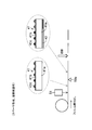
- FIG. 1 is a side view of the aerial video display device 1 of the present embodiment.
- the aerial image display device 1 reflects light from the object OB and collects it in the air on the side opposite to the object OB with respect to the aerial image display device 1, and the real image of the object OB in the air.
- R image
- the object OB may be a two-dimensional image or a three-dimensional object.
- the light from the object OB may be light emitted from the object OB itself, or light scattered to the surroundings when the object OB hits the light (scattered light). There may be.
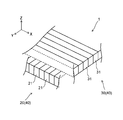
- FIG. 2 is a perspective view schematically showing a schematic configuration of the aerial video display device 1.
- the aerial video display device 1 is configured by bonding two optical panels 20 and 30 together.
- One optical panel 20 has a plurality of mirror elements 21 arranged in one direction (for example, the X direction) of two directions perpendicular to each other within a plane perpendicular to the stacking direction (for example, the Z direction) of the optical panels 20 and 30. It is formed by adhering with an adhesive.
- the other optical panel 30 is formed by arranging a plurality of mirror elements 31 in the other direction (for example, the Y direction) of the two directions and bonding them with an adhesive.
- FIG. 3 is a perspective view of one mirror element 21.
- the mirror element 21 has a rectangular parallelepiped transparent substrate 21a.
- the transparent substrate 21a extends in the Y direction, and a reflective film 21b is formed by vapor deposition on one of two opposing surfaces (for example, two surfaces along the YZ surface).
- the reflective film 21b may be formed on both opposing surfaces of the transparent substrate 21a.
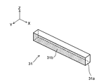
- FIG. 4 is a perspective view of one mirror element 31.
- the mirror element 31 has a rectangular parallelepiped transparent substrate 31a.
- the transparent substrate 31a extends in the X direction, and a reflective film 31b is formed by vapor deposition on one of two opposing surfaces (for example, two surfaces along the ZX surface). Note that the reflective film 31b may be formed on both opposing surfaces of the transparent substrate 31a.
- the plurality of reflective films 21b are arranged side by side in the X direction at intervals corresponding to the width of the mirror element 21 in the X direction.
- a plurality of reflection films 31b are arranged side by side in the Y direction at intervals corresponding to the width of the mirror element 31 in the Y direction.
- the reflective film 21b (reflective surface) of each mirror element 21 and the reflective film 31b (reflective surface) of each mirror element 31 are viewed in plan view (from the Z-axis direction). (See) and the positional relationship is orthogonal to each other.
- spacers for making the adhesive thickness uniform are integrally formed on the mirror elements 21 and 31, which will be described later.
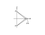
- FIG. 5 shows the imaging principle of a real image in two dimensions (in the ZX plane).
- a plurality of light rays emitted from the point light source P are respectively reflected by a reflecting surface (reflective film 21b) parallel to the Z axis, and a position P ′ opposite to the point light source P with respect to the X axis (point light source P and Condensed at a position symmetrical to the X axis).
- a real image of the point light source P is formed at the position P ′.
- FIG. 6 schematically shows the reflection of light rays in a three-dimensional space (XYZ coordinate system).
- the light beam A emitted from the point light source O is decomposed into a light beam a1 in the ZX plane and a light beam a2 in the YZ plane, and the ZX plane of the respective light beams a1 and a2 according to FIG.
- the intersection of the ray A with the Z axis can be obtained.
- the light ray a1 in the ZX plane is reflected by the reflective surface (reflective film 21b) parallel to the YZ plane and then goes to the Z axis
- the light ray a2 in the YZ plane is reflective surface (reflective) parallel to the ZX plane. After being reflected by the film 31b), it goes to the Z axis.
- These light rays a1 and a2 intersect at one point on the Z axis, that is, at the point O '. Therefore, the light ray A is reflected twice by the reflective film 21b and the reflective film 31b, and then travels toward the point O 'on the Z axis.
- FIG. 7 schematically shows a state in which a plurality of light beams emitted from the point light source O are condensed at one point via different reflecting surfaces in a three-dimensional space.
- a plurality of light rays emitted from the point light source O are reflected by the reflective surface (reflective film 21b) parallel to the YZ plane and the reflective surface (reflective film 31b) parallel to the ZX plane in the same manner as in FIG. Focus on the same point O ′ above. Thereby, a real image of the point light source O is formed at the point O ′.
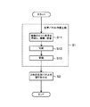
- FIG. 8 is a flowchart showing the manufacturing process of the aerial video display device 1.
- the aerial video display device 1 includes a manufacturing process (S1) for manufacturing the two optical panels 20 and 30 and a bonding process (S2) for bonding the two optical panels 20 and 30 together.
- S1 manufacturing process
- S2 bonding process
- the reflective surface of the transparent substrate 21a of one optical panel 20 produced in S1 the surface on which the reflective film 21b is formed
- the reflective surface of the transparent substrate 31a of the other optical panel 30 reflective film
- the production process of S1 further includes a lamination adhesion process (S11), a cutting process (S12), and a polishing process (S13).
- a plurality of later-described mirror elements 41 necessary for manufacturing the optical panel 40 are prepared in advance.
- the mirror element 41 manufactured in advance may be prepared, or the mirror element 41 may be manufactured and prepared on the spot.
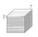
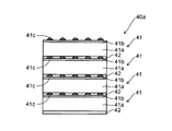
- a plurality of mirror elements 41 prepared in advance are laminated and bonded with an adhesive 42 to obtain a laminated structure 40a.
- the cutting step of S12 as shown in FIG. 10, the laminated structure 40a is cut at equal intervals with a wire saw or the like.
- the cutting line is shown with the broken line.
- the polishing step of S13 the cut surface of each structure obtained by cutting is polished. Thereby, the some optical panel 40 is obtained.
- the laminated structure 40a may be formed in a shape that matches the shape of the optical panel 40 shown in FIG. In this case, since the optical panel 40 is completed at the same time when the laminated structure 40a is formed, the above-described cutting process and polishing process become unnecessary.
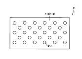
- FIG. 11A is a plan view of one mirror element 41
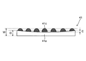
- FIG. 11B is a cross-sectional view taken along line AA ′ in FIG. 11A.
- the mirror element 41 is a structure in which a transparent substrate 41a, a reflective film 41b, and a spacer 41c are integrally formed.
- the transparent substrate 41a is made of transparent glass or resin.
- the thickness of the transparent substrate 41a is usually set to 0.1 mm to 1 mm in consideration of resolution. For example, when the transparent substrate 41a is made of glass, the thickness is about 0.5 mm, and when the transparent substrate 41a is made of resin, the thickness is about 0.2 mm.
- the reflection film 41b is composed of a single layer film made of a single metal such as aluminum, or a multilayer film containing a metal or a dielectric, and the film thickness is appropriately controlled so that all incident light is reflected. .
- the reflective film 41b is formed on at least one of the two opposing surfaces of the transparent substrate 41a. That is, the reflective film 41b may be formed on both surfaces of the transparent substrate 41a as shown in FIG. 11B, or may be formed only on one surface of the transparent substrate 41a as shown in FIGS. .
- the thickness is, for example, about 100 nm.
- the spacer 41c is a projecting portion (projecting portion) projecting in the thickness direction from the transparent substrate 41a, and is formed in an independent island shape.
- the “spacer” here refers to a portion (shape, structure) having a protruding height, and does not include a flat portion between the spacers.
- the spacer 41c has two opposing surfaces of the transparent substrate 41a in order to make the thickness (adhesion thickness) of the adhesive 42 shown in FIG. 10 uniform and to make the sum of the thickness of the transparent substrate 41a and the adhesion thickness uniform. Are formed discretely in advance on one surface side.
- the spacer 41c may be formed on the transparent substrate 41a via the reflective film 41b as shown in FIG. 11B and FIG. 13, or may be directly formed on the transparent substrate 41a as shown in FIG. .
- the spacers 41c are arranged in a matrix in a plan view, and the arrangement pitch P1 in the row direction and the arrangement pitch P2 in the column direction are set to 1 mm, for example. Further, the height T of all the spacers 41c is set within a range of 20 ⁇ m ⁇ 1 ⁇ m, for example. As described above, the spacer 41c is formed at a predetermined height at a predetermined position with respect to the transparent substrate 41a.
- the lamination bonding step includes a preparation step of preparing a plurality of mirror elements 41 in advance and a bonding step of stacking the prepared plurality of mirror elements 41 and bonding them with the adhesive 42.
- a plurality of mirror elements 41 in which the transparent substrate 41a, the reflective film 41b, and the spacer 41c are integrally formed, are prepared in advance, and the spacer 41c is positioned between the transparent substrates 41a.
- the spacer 41c of one mirror element 41 adjacent in the laminating direction is brought into contact with the other mirror element 41 (transparent substrate 41a or reflective film 41b).
- the thickness of the adhesive 42 is defined by the height of the spacer 41c, and variations in the thickness of the adhesive 42 are less likely to occur.
- the thickness of the transparent substrate 41a varies, the thickness of the transparent substrate 41a and the height of the spacer 41c (the thickness of the adhesive 42) are adjusted by adjusting the height of the spacer 41c. It is also possible to make it constant in a direction perpendicular to the thickness (details will be described later). Thereby, the parallelism of the reflective surface (surface in which the reflective film 41b was formed) of each transparent substrate 41a is securable favorably. For example, the angle shift of each reflecting surface can be suppressed to 0.025 degrees or less.
- the above-described effect that the parallelism of each reflecting surface can be ensured can be easily obtained by a simple method in which a plurality of mirror elements 41 integrated with spacers 41c are used and stacked. As a result, the productivity of the optical panel 40 can be improved. That is, according to the manufacturing method of this embodiment, it is possible to achieve both the placement accuracy and productivity of each reflecting surface.
- the thickness of the adhesive 42 can be kept constant by the spacer 41c. Therefore, when the thickness of each transparent substrate 41a is constant, the parallelism of the reflective surface of each transparent substrate 41a can be ensured satisfactorily.
- the spacers 41c are arranged in a matrix in a plan view, when the adhesive 42 is filled between the transparent substrates 41a, the adhesive 42 is interposed between the adjacent spacers 41c and 41c. Spread evenly. Further, between the adjacent spacers 41c and 41c, the adhesive 42 is in direct contact with the transparent substrate 41a or the reflective film 41b. Therefore, the matrix arrangement of the spacers 41c is suitable for securing the flow path and the bonding area of the adhesive 42.
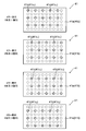
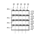
- FIG. 15 shows the arrangement positions of the spacers 41c of the four mirror elements 41 arranged in the stacking direction.
- the first (first layer), second (second layer), third (third layer), and fourth (fourth layer) mirror elements 41 from one side in the stacking direction each spacer 41c, respectively, and spacers 41c 1, 41c 2, 41c 3 , 41c 4.
- the spacer 41c 2 is disposed with a half pitch (for example, 0.5 mm) in the row direction with respect to the spacer 41c 1
- the spacer 41c 3 is a half pitch (for example, 0.5 mm) with respect to the spacer 41c 2 in the column direction.
- the spacer 41c 4 is displaced by a half pitch (for example, 0.5 mm) in the row direction with respect to the spacer 41c 3 and is a half pitch (for example, 0.5 mm) in the column direction with respect to the spacer 41c 1 . ) It is shifted.
- the spacers 41c (41c 1 to 41c 4 ) are arranged at the same position in plan view (viewed from the stacking direction), the position where the spacer 41c does not exist, that is, the position where the adhesive 42 is filled is also shown in plan view. It becomes the same position.
- the spacer 41c of one mirror element 41 adjacent in the stacking direction is perpendicular to the stacking direction with respect to the spacer 41c of the other mirror element 41 (corresponding to the above row direction and column direction).
- FIG. 16 shows another arrangement example of the spacer 41c.
- the spacers 41c may be arranged in a staggered pattern on one surface side of the transparent substrate 41a.
- the staggered arrangement refers to a mode in which the spacers 41c are arranged with a half pitch shift in the column direction between adjacent rows, or the spacers 41c are arranged with a half pitch shift in the row direction between adjacent columns. Even when the spacers 41c are arranged in a staggered pattern, it can be seen that the spacers 41c are arranged in a matrix when the mirror element 41 is rotated 45 degrees in plan view. That is, the staggered arrangement is a kind of matrix arrangement.
- the flow path and the bonding area of the adhesive 42 can be secured.
- the spacer 41c of one mirror element 41 adjacent in the stacking direction is shifted from the spacer 41c of the other mirror element 41 in a direction perpendicular to the stacking direction, and the adhesive is used. You may make it reduce the unevenness
- FIG. in addition, the arrangement of the spacers 41c may be a random arrangement.
- the spacer 41c is formed on the reflective film 41b as shown in FIG. 11B and FIG. 13, other members are less likely to come into direct contact with the reflective film 41b when the mirror element 41 is transported or laminated. (Because the member first contacts the spacer 41c). Therefore, the configuration in which the spacer 41c is formed on the reflective film 41b is advantageous in that the reflective film 41b is less likely to be damaged than the configuration in which the spacer 41c is directly formed on the transparent substrate 41a (see FIG. 12). is there.
- the spacer 41c can be formed of an energy curable resin, a pigment-based resin (including a resin, a pigment, and a solvent), a resin that is cured by a chemical reaction at room temperature (for example, an epoxy-based resin), and the like. It is desirable that it is made of a functional resin.
- the energy curable resin is a resin that is cured by applying energy such as heat or light from the outside, such as a thermosetting resin or a photocurable resin. Since the energy curable resin has little volume change at the time of curing and is chemically stable, the spacer 41c can be efficiently formed at a predetermined height at a predetermined position, and is suitable as a resin for spacer formation. It is.
- the spacer 41c and the adhesive 42 are preferably transparent and have substantially the same refractive index as that of the transparent substrate 41a. In this case, scattering of light and reflection of stray light at the interface between any two of the spacer 41c, the adhesive 42, and the transparent substrate 41a can be reduced, and deterioration of the aerial image due to scattered light and stray light can be prevented. it can.
- a glass having a refractive index of 1.52 to 1.53 is used as the transparent substrate 41a
- a transparent ultraviolet (UV) curable resin having a refractive index of 1.53 is used as the spacer 41c, and the adhesive 42 is refracted.
- the above effect can be obtained by using a transparent epoxy adhesive having a rate of 1.528.
- the refractive index difference among the transparent substrate 41a, the spacer 41c, and the adhesive 42 is preferably within a range of ⁇ 0.01.
- the material of the spacer 41c is liquid, and the shape of the spacer 41c is preferably circular when viewed from the stacking direction. That is, it is desirable that the spacer 41c is made of a material having fluidity before being cured and is circular in plan view.
- the material having fluidity in addition to the energy curable resin and the pigment-based resin described above, the ink described later can be used.
- the spacer has an angular shape in a plan view or a linear spacer, the droplet that becomes the spacer is attached to the substrate and is cured by the influence of the surface tension or the like until it cures. The shape changes. At this time, if the spacer has corners, the variation in shape increases. Further, when the spacer is linear, the shape error increases as the amount of liquid in one plane and the contact area with the substrate increase.
- the shape of the spacer 41c is circular, a spacer having a uniform height and shape is easily obtained.
- the spacer 41c is preferably formed by ink jet printing.
- inkjet printing ink droplets can be landed accurately at a desired position, and the height of the landed ink can be easily adjusted by controlling the number of ink droplets landed at the same position. .
- the spacer 41c can be formed at a predetermined position at a predetermined height with high accuracy and efficiency.
- the ink containing the material which forms the spacer 41c mentioned above can be used as an ink used for inkjet printing.
- an ink containing no volatile component for example, an ink made of an energy curable resin
- an ink containing a volatile component for example, a pigment Ink
- drying the ink after landing makes the ink height lower than before drying because the solvent contained in the ink volatilizes.
- the spacer 41c is desirably formed at a height corresponding to the amount of depression on the surface of the transparent substrate 41a or the thickness of the transparent substrate 41a.
- the amount of depression and the thickness may be obtained by measurement immediately before ink is ejected, or may be a value acquired in advance (for example, a value measured when the transparent substrate 41a is manufactured). Also good.
- the spacer 41c By forming the spacer 41c as described above, variations in the amount of depression and thickness of the surface of the transparent substrate 41a can be corrected by the spacer 41c. Specifically, as shown in FIG. 17, even if there is variation in the amount of depressions (amount indicated by C in the figure) and thickness (amount indicated by D in the figure) on one transparent substrate 41a, the transparent substrate The sum W of the thickness of 41a and the height of the spacer 41c can be made substantially constant in a direction perpendicular to the thickness direction of the transparent substrate 41a.
- the reflection film 41b formed on the front and back of the transparent substrate 41a is not shown.
- the spacer 41c can correct variations in the dent amount and thickness of the surface of the transparent substrate 41a, the parallelism of the reflecting surfaces of the transparent substrates 41a can be reliably improved.
- the aerial video display device 1 configured using the optical panel 40 can display a high-quality video with little distortion in the air.
- FIG. 18 schematically shows an example in which the spacer 41c is formed by ink jet printing.
- the displacement meter 52 is composed of a distance measuring sensor that measures the distance to the surface of the transparent substrate 41a, for example. Using the distance between the displacement meter and the transparent substrate at the measurement start position (for example, the edge of the substrate) as a reference, this distance and the distance between the displacement meter and the transparent substrate measured at each position in the direction perpendicular to the substrate thickness direction. By obtaining the difference, the amount of depression on the surface of the transparent substrate 41a can be obtained for each measurement position.
- the displacement meter 52 may not be installed. Further, instead of measuring the amount of depression, the thickness may be measured for each position of the transparent substrate 41a.
- ink for example, UV curable resin
- inkjet head 51 is ejected from the inkjet head 51 to a predetermined position on the transparent substrate 41a so that the spacer 41c is formed at a height corresponding to the amount of depression on the surface of the transparent substrate 41a.
- the number of ink droplet ejections at the same position is not limited as long as the spacer 41c is formed at a desired height, and may be once or a plurality of times.
- the ink is cured by UV irradiation from the UV light source 53.
- the spacer 41c is formed at a desired height at a predetermined position.
- the spacer 41c is preferably formed by ejecting one drop of ink (the number of ejections at the same position is desirably one). This is because if the spacer 41c is formed by a plurality of ink ejections, the height may vary when ejection misalignment (printing position misalignment) occurs. In other words, the spacer 41c is formed by discharging one drop of ink, whereby the spacer 41c having excellent height accuracy can be formed.
- the piezoelectric body which may be a piezoelectric thin film
- the piezoelectric body is expanded and contracted, and pressure is applied to the ink in the pressure chamber.
- Ink discharge is performed.
- the amount of ink discharged at one time can be changed by adjusting the drive waveform (drive voltage, voltage application time, etc.) of the drive signal. Therefore, the height of the spacer 41c formed by ejecting one drop of ink can be adjusted by adjusting the drive waveform.
- the spacer 41c may be formed by screen printing. Even when screen printing is used, the spacer 41c can be formed at a predetermined position at a predetermined height with high accuracy and efficiency.
- the spacer 41c may be black.
- the black spacer 41c can be realized by adding a black pigment or carbon black to the resin constituting the spacer 41c. If the spacer 41c is black, light incident on the spacer 41c is absorbed there, and therefore no light scattering or stray light reflection occurs on the surface of the spacer 41c. Accordingly, it is possible to reduce the deterioration of the aerial image due to scattered light or stray light.
- the spacer 41c may be formed of the same material as the transparent substrate 41a.
- both the spacer 41c and the transparent substrate 41a may be formed of glass or may be formed of resin.
- the spacer 41c is formed by pressing the mold against the transparent substrate 41a, the spacer 41c and the transparent substrate 41a are integrally formed by injection molding, or the surface of the transparent substrate 41a is etched to form the spacer 41c. It is possible to form the spacer 41c by various methods such as forming.
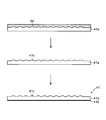
- FIG. 19 is a cross-sectional view showing an example of the manufacturing process of the mirror element 41.
- the spacer 41c pushes the negative mold 54 in which the shape of the spacer 41c is inverted against the transparent substrate 41a (before curing).
- the shape may be integrally formed with the transparent substrate 41a by transferring the shape to the transparent substrate 41a.
- the spacer 41c excellent in height accuracy can be formed at a predetermined position of the transparent substrate 41a.
- both the spacer 41c and the transparent substrate 41a are formed of resin, they may be integrally formed by injection molding, and even in this case, the same effect as described above can be obtained.
- the mirror element 41 is completed, for example, by forming the reflective film 41b on the back surface of the transparent substrate 41a (the surface opposite to the side on which the spacer 41c is formed).
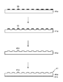
- FIG. 20 is a cross-sectional view showing another example of the manufacturing process of the mirror element 41.
- the transparent substrate 41a is made of glass, and the spacer 41c may be formed by etching the transparent substrate 41a.
- a mask 55 made of a resist or a film is formed on the transparent substrate 41a, and an unmasked portion of the transparent substrate 41a is dug by etching, so that the unetched portion remains as the spacer 41c. Accordingly, even in this case, the spacer 41c can be formed at a predetermined position of the transparent substrate 41a, and the spacer 41c having excellent height accuracy can be formed by managing the etching amount.
- the parallelism of the reflecting surface is determined only by the thickness accuracy of the original transparent substrate 41a, the parallelism of the reflecting surface is ensured by managing the thickness of the transparent substrate 41a with high accuracy. Can do.
- FIG. 21 is a cross-sectional view showing still another example of the manufacturing process of the mirror element 41.
- the spacer 41c is formed by applying an energy curable resin 56a on a transparent substrate 41a made of glass, for example, and curing the energy curable resin 56a while pressing the negative mold 57 in which the shape of the spacer 41c is reversed. It may be formed by forming and releasing. In this case, a portion having a protruding height in the cured film 56 becomes the spacer 41c. Thus, even when the transparent substrate 41a and the spacer 41c are made of different materials, the spacer 41c can be formed at a predetermined position on the transparent substrate 41a with high accuracy.
- the height of the spacer 41c is desirably 1 ⁇ m to 100 ⁇ m.
- the thickness of the adhesive 42 can be ensured by 1 ⁇ m or more.
- the adhesive 42 can be sufficiently spread between the transparent substrates 41a and 41a arranged in the stacking direction, and sufficient adhesive strength can be ensured.
- the spacer 41c can be surely brought into contact with the transparent substrate 41a to ensure the parallelism of each reflecting surface.
- the spacer 41c when the height of the spacer 41c is 100 ⁇ m or less, it is difficult for bubbles to be involved when the adhesive 42 is filled, and light scattering in the adhesive 42 is less likely to occur. Further, distortion and warpage of the transparent substrate 41a due to curing shrinkage of the adhesive 42 are less likely to occur, which can contribute to ensuring the parallelism of each reflecting surface.
- the diameter of the spacer 41c is L ( ⁇ m) and the height is T ( ⁇ m)
- the diameter L is preferably 1 to 1000 ⁇ m
- the aspect ratio (T / L) is 1 to 1/300 is desirable.
- the total area of the spacers 41c is desirably 10% or less of the area of the reflective surface (surface on which the reflective film 41b is formed) in the transparent substrate 41a.
- the total area of the spacers 41c is represented by ⁇ (L / 2) 2 ⁇ (number of spacers included in one mirror element).
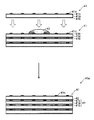
- FIG. 22 shows an example of a technique in which a plurality of mirror elements 41 are stacked and bonded.
- a step of applying an adhesive 42 on the mirror element 41 and (2) a step of laminating another mirror element 41 on the mirror element 41 via the adhesive 42. , May be repeated. That is, the adhesive 42 may be supplied onto the mirror element 41, and the mirror element 41 (transparent substrate 41a) may be sequentially stacked and bonded.
- each mirror element 41 can be laminated
- the thickness of the adhesive 42 can be defined by the height of the spacer 41c, and the laminated structure 40a with little variation in the thickness of the adhesive 42 can be obtained.
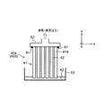
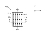
- FIG. 23 shows another example of the lamination adhesion method, and corresponds to a cross-sectional view taken along line B-B ′ of FIG.
- the plurality of mirror elements 41 may be arranged in a stacked manner, and the adhesive 42 may be simultaneously injected into all the gaps between the transparent substrates 41a adjacent to each other in the stacking direction. .
- the stacking direction of the plurality of mirror elements 41 is the z direction, and two directions perpendicular to each other in the plane perpendicular to the z direction are the x direction and the y direction.
- the xyz directions are different from the XYZ directions shown in FIG.
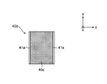
- FIG. 24 and FIG. 25 in a laminated body 40b in which a plurality of mirror elements 41 are arranged so that a spacer 41c is positioned between the transparent substrates 41a, each surface is arranged on two surfaces facing each other in the x direction.
- Adhesive film 40c is affixed so that it may cover. Thereby, the clearance gap between each transparent substrate 41a * 41a of the laminated body 40b is sealed except a y direction.
- one end side of the laminated body 40 b in the y direction is fixed to the suction nozzle 62 via the packing 61, and the other end side is used by the adhesive 42 put in the container 63.
- the stacked body 40b is disposed.
- the viscosity of the adhesive 42 is preferably 1000 mPa ⁇ s or less, and more preferably 200 mPa ⁇ s or less. Thereby, the adhesive agent 42 can be smoothly filled in the clearance gap between each transparent substrate 41a * 41a of the laminated body 40b.
- the degree of vacuum in the gap is preferably 0.05 MPa or less, more preferably 0.01 MPa, during suction by the vacuum pump.
- the adhesive agent 42 can be filled more smoothly into the gap between the transparent substrates 41a and 41a.
- the spacer 42c of one mirror element 41 adjacent in the stacking direction is also brought into contact with the other mirror element 41 by injecting the adhesive 42 by differential pressure and bonding the plurality of mirror elements 41.
- each mirror element 41 can be adhered. Therefore, the thickness of the adhesive 42 can be defined by the height of the spacer 41c, and the laminated structure 40a with little variation in the thickness of the adhesive 42 can be obtained.
- the adhesive 42 used for bonding the mirror elements 41 described above may be an epoxy adhesive.
- a two-component mixed epoxy adhesive which is a mixture of a base material composed of an epoxy resin and a curing agent, has a small shrinkage in curing, so that the distortion of the transparent substrate 41a is small and the parallelism of the reflecting surface is ensured. It is advantageous in that it is easy to do.
- the hardness after hardening of the said adhesive agent is high (because it is hard), there also exists an advantage that the process of the subsequent cutting
- the adhesive 42 may be a thermosetting adhesive.
- the thermosetting adhesive is suitable for accurately laminating and bonding the transparent substrate 41a provided with the reflective film 41b with an adhesive thickness of 1 to 100 ⁇ m.
- the adhesive 42 may be an anaerobic adhesive.
- An anaerobic adhesive is an adhesive that hardens only when the air (oxygen) is blocked. As described above, even if an anaerobic adhesive is used as the adhesive 42, the transparent substrate 41a including the reflective film 41b can be laminated and adhered with a thickness of 1 to 100 ⁇ m with high accuracy.
- the outermost layer of the reflective film 41b be a metal.
- the reflective film 41b may be a metal such as aluminum in the case of a single layer film, and the outermost layer may be a metal such as aluminum in the case of a multilayer film. Since the anaerobic adhesive 42 blocks air and cures by reacting with the metal, if the outermost layer of the reflective film 41b is a metal, the anaerobic adhesive 42 is used to attach the reflective film 41b.
- the transparent substrate 41a can be laminated and bonded.
- the curing time of the adhesive is preferably 24 hours or longer.
- the curing time of the adhesive is a time required for the tensile shear adhesive strength (adhesive surface: 12.5 mm ⁇ 25 mm) of the single overlap to reach 10 N / mm 2 or more at 23 ° C.
- an adhesive (adhesive) tape having adhesive layers on both sides of the substrate may be used, and the adhesive layer may be utilized as the adhesive 42.
- a photocurable adhesive for example, a UV adhesive
- the method for manufacturing the optical panel 40 of the present embodiment may include a cutting step.
- the cutting step the laminated structure 40a is cut perpendicularly to the surface on which the reflective film 41b is formed (see FIG. 30).
- a plurality of optical panels 40 can be obtained from one laminated structure 40a, so that the productivity of the optical panel 40 can be improved with certainty. Since the cut surface is rough after cutting, it is desirable to polish it (polishing step).
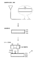
- the mirror element 41 is produced. That is, as shown in FIG. 26, the molten material is molded into a substrate and cut to obtain a transparent substrate 41a.
- the transparent substrate 41a can be produced by using a fusion method, and in the case of a resin material, the transparent substrate 41a can be produced by extrusion molding.
- a metal material for example, aluminum
- UV ink is ejected onto the reflective film 41 b by the inkjet head 51, and UV light is irradiated and cured by the UV light source 53 to form the spacer 41 c.
- the spacer 41c is formed with a height that can correct the thickness variation of the transparent substrate 41a.
- the mirror element 41 which integrated the transparent substrate 41a, the reflective film 41b, and the spacer 41c is obtained. By repeating this process, a plurality of mirror elements 41 are produced.
- an adhesive 42 is applied to the mirror element 41 to laminate and bond the other mirror element 41, and this process is repeated to obtain a laminated structure 40a.
- the reflective film 41b of each mirror element 41c appears periodically in the stacking direction (aligned in parallel at a predetermined interval in the stacking direction).
- the laminated structure 40a is cut at regular intervals along a plane perpendicular to the reflection surface (reflection film 41b). After cutting, the cut surface is polished to obtain the optical panel 40 (see FIG. 10).
- the two optical panels 40 are bonded together to obtain an aerial image display device.
- the surface of the transparent substrate 41a of one optical panel 40 on which the reflective film 41b is formed and the surface of the transparent substrate 41a of the other optical panel 40 on which the reflective film 41b is formed are orthogonal to each other in plan view.
- Two optical panels 40 are bonded together.
- One optical panel 40 corresponds to the optical panel 20 of FIG. 2, and the reflective film 41b of the optical panel 40 corresponds to the reflective film 21b of FIG.
- the other optical panel 40 corresponds to the optical panel 30 in FIG. 2, and the reflective film 41b of the optical panel 40 corresponds to the reflective film 31b in FIG. Therefore, the aerial video display device 1 shown in FIGS. 1 and 2 can be obtained by bonding the two optical panels 40 together as described above.
- an aerial video display device was actually manufactured as follows. That is, a glass substrate having a length of 250 mm, a width of 400 mm, and a thickness of 0.5 mm is used as the transparent substrate 41a, and a reflective film 41b is formed on both surfaces thereof by an aluminum coat (thickness of 100 nm), and one surface of the transparent substrate 41a is formed. On the side, dots (spacer 41c) having a diameter of 0.1 mm and a height of 20 ⁇ m ⁇ 1 ⁇ m were printed at a pitch of 1 mm in the vertical and horizontal directions using UV ink, and the mirror element 41 was produced.
- each mirror element 41 is displaced by (0, 0), (0.5, 0), (0.5 , 0.5) and (0, 0.5) in order, the layers were laminated via the adhesive 42, and the adhesive 42 was cured.
- the adhesive 42 was cured.
- the obtained laminated structure 40a was cut into a width of 2 mm with a wire slicer and then polished to a width of 1.5 mm. As a result, it was possible to obtain the optical panel 40 having a uniform bonding thickness of 20 ⁇ m ⁇ 1 ⁇ m.
- a plurality of mirror elements 41 are produced as follows. As shown in FIG. 27, a transparent PET (polyethylene terephthalate) film wound in a roll shape is prepared and used as the transparent substrate 41a. Then, aluminum is sputter-deposited on one surface side of the PET film drawn out from the roll, and a reflective film 41b is formed on the transparent substrate 41a.
- the PET film on which the reflective film 41b is formed may be wound up in a roll shape, or may be introduced into the next step as it is without being wound up.
- a spacer 41c is formed on the reflective film 41b of the transparent substrate 41a by inkjet printing using the inkjet head 51.
- an anaerobic adhesive 42 is applied to the back surface of the transparent substrate 41a, that is, the surface opposite to the side on which the reflective film 41b is formed, by a coater 59a, and then the transparent substrate 41a is applied every predetermined length. Disconnect. Thereby, a plurality of mirror elements 41 with the adhesive 42 are obtained.
- a plurality of mirror elements 41 are laminated via an adhesive 42 so that spacers 41c are positioned between the transparent substrates 41a.
- the adhesive 42 comes into contact with the reflective film 41b made of metal, the adhesive 42 starts to be cured simultaneously with the lamination, and strong adhesion can be performed. Note that the space around the adhesive 42 may be decompressed. Even if the adhesive 42 is difficult to be cured by such a reduced pressure, the entire adhesive can be uniformly cured. Thus, the laminated structure 40a is obtained.
- the laminated structure 40a is cut perpendicularly (along the broken line in the drawing) to the surface on which the reflective film 41b is formed. Thereby, the some optical panel 40 is obtained.
- the aerial video display device 1 is obtained by bonding the two optical panels 40 together.
- an aerial image display device was actually manufactured as follows. That is, a transparent PET film having a thickness of 0.2 mm and a width of 250 mm was prepared as the transparent substrate 41a, the films were sequentially fed from the roll, and aluminum was sputtered on one surface thereof to form a reflective film 41b having a thickness of 100 nm. . Then, a spacer 41c having a height of 10 ⁇ m was formed on the reflective film 41b by ink jet printing.
- an anaerobic adhesive (Alontite UL, manufactured by Toagosei Co., Ltd.) was applied at a thickness of 10 ⁇ m on the side opposite to the surface on which the reflective film 41b of the transparent base material 41a was formed, and cut every 400 mm in length. .
- a mirror element 41 with an adhesive in which a reflective film 41b and a spacer 41c are formed on one side of a transparent substrate 41a having a length of 250 mm, a width of 400 mm, and a thickness of 0.2 mm, and an adhesive 42 is applied to the other side.
- an adhesive 42 is applied to the other side.
- the obtained mirror elements 41 were sequentially laminated.
- the adhesive 42 was cured by contact with the reflective film 41b, and a laminated structure 40a was obtained. Thereafter, the obtained laminated structure 40a was cut and polished in the same manner as in Example 1 to obtain the optical panel 40.
- the aerial image display device 1 having excellent imaging quality is obtained. I was able to.
- optical panel 40 (see FIG. 30 and the like) manufactured by the manufacturing method described above can be expressed as follows. That is, the optical panel 40 of the present embodiment is an optical panel 40 used in the aerial video display device 1 that displays an aerial video, and includes a plurality of mirror elements 41. In the mirror element 41, a reflective film 41b is formed on at least one of the two opposing surfaces of the transparent substrate 41a, and spacers 41c are previously discretely formed on one of the two surfaces. It is. The plurality of mirror elements 41 are laminated so that the spacers 41c are positioned between the transparent substrates 41a and bonded with an adhesive 42.
- the thickness of the adhesive 42 between the transparent substrates 41a and 41a is defined by the height of the spacer 41c, and the thickness of the adhesive 42 is less likely to vary.
- the parallelism of the reflective surface of each transparent substrate 41a can be ensured satisfactorily.
- the parallelism of each reflecting surface can be easily ensured by adopting a configuration in which a plurality of mirror elements 41 each having the spacer 41c integrated therein are laminated. As a result, the productivity of the optical panel 40 can be improved.
- the spacer structure by adopting the spacer structure, the parallelism of each reflecting surface can be ensured as described above, so that the optical panel 40 and thus the aerial image display device 1 can be enlarged, and a large and high-definition image is displayed.
- the aerial video display device 1 (see FIGS. 1 and 2) can be realized.
- the spacer 41c of one mirror element 41 adjacent in the stacking direction is in contact with the other mirror element 41.
- the thickness of the adhesive 42 can be kept constant by the spacer 41c, the parallelism of the reflecting surface of each transparent substrate 41a can be ensured reliably.
- the aerial video display device 1 includes two optical panels 40 described above. Then, the reflective surface of the transparent substrate 41a of one optical panel 40 (the surface on which the reflective film 41b is formed) and the reflective surface of the transparent substrate 41a of the other optical panel 40 (the surface on which the reflective film 41b is formed). Two optical panels 40 and 40 are bonded together so as to be orthogonal in a plan view. In each optical panel 40, since the parallelism of the reflecting surfaces arranged in the stacking direction can be ensured satisfactorily, the aerial video display device 1 configured by bonding these optical panels 40 and 40 has high definition. Video (video with reduced distortion) can be displayed.
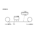
- the optical panel 40 of this embodiment can also be manufactured as follows. As shown in FIG. 31, a transparent PET film wound in a roll shape is prepared and used as the transparent substrate 41a. Then, aluminum is sputtered on one side (back side) of the PET film fed from the roll, and a reflective film 41b is formed on the back side of the transparent substrate 41a.
- the PET film on which the reflective film 41b is formed may be wound up in a roll shape, or may be introduced into the next step as it is without being wound up.
- the surface of the transparent substrate 41a (the surface opposite to the side where the reflective film 41b is formed) is coated with a UV curable resin as the energy curable resin 56a by the coater 59b.
- a UV curable resin as the energy curable resin 56a by the coater 59b.
- UV light is irradiated from the UV light source 53 while pressing with a negative mold 57 (here, a roller having a negative shape) in which the shape of the spacer 41c is reversed, and then the energy curable resin 56a is cured and then released.
- a negative mold 57 here, a roller having a negative shape
- mold 57 it is desirable to use transparent molds, such as quartz.
- the energy curable resin 56 a can be irradiated with UV light and cured through the negative mold 57.
- the material which forms the cured film 56 spacer 41c is not specifically limited, You may use a thermosetting resin. Further, the method of forming the cured film 56 is not limited to the above method.
- an adhesive tape 60 with an adhesive on both surfaces of the base material is attached on the reflective film 41b of the transparent substrate 41a, and the transparent substrate 41a is cut at predetermined lengths.
- a mirror film 41c with an adhesive in which a cured film 56 having a spacer 41c is formed on one surface of the transparent substrate 41a and an adhesive 42 (adhesive of the adhesive tape 60) is provided on the other surface. Is obtained.
- the some mirror element 41 is laminated
- a laminated structure 40a in which a plurality of mirror elements 41 are laminated and bonded is obtained.
- the spacer 41 c enters the adhesive on the surface of the adhesive tape 60 and contacts the base material of the adhesive tape 60.
- the laminated structure 40a is cut perpendicularly to the surface on which the reflective film 41b is formed, so that a plurality of optical panels 40 are obtained.
- the aerial video display device 1 is obtained by bonding the two optical panels 40 together.
- optical panel The optical panel, the optical panel manufacturing method, the aerial video display device, and the aerial video display device manufacturing method of the present embodiment described above may be expressed as follows.
- a reflective film is formed on at least one of two opposing surfaces of a transparent substrate, and a spacer is previously formed in a matrix on one surface of the two opposing surfaces.
- a plurality of discretely formed mirror elements are used, and the plurality of mirror elements are stacked and bonded with an adhesive so that the spacer is positioned between the transparent substrates.
- the spacer of one mirror element adjacent in the stacking direction is in contact with the other mirror element.
- the spacer may be formed on the reflective film.
- the spacer may be formed of an energy curable resin.
- the spacer of one mirror element adjacent in the stacking direction is shifted from the spacer of the other mirror element in a direction perpendicular to the stacking direction.
- the material of the spacer is liquid, and the shape of the spacer is circular when viewed from the stacking direction.
- the spacer and the adhesive may be transparent and may have substantially the same refractive index as the transparent substrate.
- the spacer is preferably formed by ink jet printing.
- the spacer may be formed with a height corresponding to the amount of depression on the surface of the transparent substrate or the thickness of the transparent substrate.
- the spacer is preferably formed such that the sum of the thickness of the transparent substrate and the height of the spacer is substantially constant in a direction perpendicular to the thickness direction of the transparent substrate.
- the spacer is preferably formed by discharging one drop of ink.
- the spacer may be formed by screen printing.
- the spacer may be black.
- the spacer may be formed of the same material as the transparent substrate.
- the spacer may be formed by pressing a negative mold in which the shape of the spacer is inverted against the transparent substrate, and transferring the shape to the transparent substrate.
- the spacer may be made of resin together with the transparent substrate, and may be formed by injection molding.
- the transparent substrate may be made of glass, and the spacer may be formed by etching the transparent substrate.
- the spacer is coated with the energy curable resin on the transparent substrate, and the energy curable resin is cured in a state where a negative mold in which the shape of the spacer is reversed is pressed. It may be formed by doing.
- the height of the spacer is desirably 1 ⁇ m to 100 ⁇ m.
- the step of applying the adhesive on the mirror element, and another mirror element on the mirror element via the adhesive And laminating may be repeated.
- the plurality of mirror elements are stacked and the adhesive is simultaneously injected into all the gaps between the transparent substrates adjacent in the stacking direction. It may be glued.
- the adhesive may be an epoxy adhesive.
- the adhesive may be a thermosetting adhesive.
- the adhesive may be an anaerobic adhesive.
- the outermost layer of the reflective film is preferably a metal.
- the above manufacturing method may further include a step of cutting the laminated structure in which the plurality of mirror elements are laminated and bonded with an adhesive perpendicularly to the surface on which the reflective film is formed.
- An aerial image display device manufacturing method is an aerial image display device manufacturing method including the optical panel manufacturing method described above, and includes two optical panels manufactured by the optical panel manufacturing method. Among the two optical panels, the surface on which the reflective film of the transparent substrate of one optical panel is formed and the surface of the transparent substrate of the other optical panel on which the reflective film is formed are orthogonal to each other in plan view. The process which sticks together.
- the optical panel of the present embodiment is an optical panel used in an aerial image display device that displays an aerial image, and a reflective film is formed on at least one of two opposing surfaces of a transparent substrate, and the opposing surfaces are opposed to each other.
- a plurality of mirror elements in which spacers are discretely formed in a matrix in advance are provided on one of the two surfaces, and the plurality of mirror elements are stacked so that the spacers are positioned between the transparent substrates. Are bonded with an adhesive.
- the spacer of one mirror element adjacent in the stacking direction is in contact with the other mirror element.
- the aerial image display device includes two optical panels as described above, and a surface on which a reflective film is formed on the transparent substrate of one optical panel and a reflective film on the transparent substrate of the other optical panel are formed.
- the two optical panels are bonded so that the surface is orthogonal to the plane view.
- the method for manufacturing an optical panel of the present invention can be used for manufacturing an optical panel constituting an aerial image display device, for example.
Landscapes
- Physics & Mathematics (AREA)
- General Physics & Mathematics (AREA)
- Optics & Photonics (AREA)
- Optical Elements Other Than Lenses (AREA)
Abstract
Dans la présente invention, un procédé de fabrication d'un panneau optique comprend une étape de stratification et de collage. Dans l'étape de stratification et de collage, un film réfléchissant est formé sur au moins une surface parmi deux surfaces de face de substrats transparents, et une pluralité d'éléments miroirs est utilisée sur une surface parmi les deux surfaces indiquées ci-dessus, une matrice d'entretoises individuelles étant formée à l'avance sur ledit élément. La pluralité d'éléments miroirs est stratifiée et collée en utilisant un adhésif de façon que les entretoises soient positionnées entre les substrats transparents.
Priority Applications (2)
| Application Number | Priority Date | Filing Date | Title |
|---|---|---|---|
| CN201680042814.9A CN108027462A (zh) | 2015-07-22 | 2016-07-19 | 光学面板、光学面板的制造方法、空中影像显示设备以及空中影像显示设备的制造方法 |
| JP2017522444A JPWO2017014221A1 (ja) | 2015-07-22 | 2016-07-19 | 光学パネルの製造方法よび空中映像表示デバイスの製造方法 |
Applications Claiming Priority (2)
| Application Number | Priority Date | Filing Date | Title |
|---|---|---|---|
| JP2015145080 | 2015-07-22 | ||
| JP2015-145080 | 2015-07-22 |
Publications (1)
| Publication Number | Publication Date |
|---|---|
| WO2017014221A1 true WO2017014221A1 (fr) | 2017-01-26 |
Family
ID=57834338
Family Applications (1)
| Application Number | Title | Priority Date | Filing Date |
|---|---|---|---|
| PCT/JP2016/071171 Ceased WO2017014221A1 (fr) | 2015-07-22 | 2016-07-19 | Panneau optique, procédé de fabrication de panneau optique, dispositif d'affichage de vidéo dans l'air, et procédé de fabrication de dispositif d'affichage de vidéo dans l'air |
Country Status (3)
| Country | Link |
|---|---|
| JP (1) | JPWO2017014221A1 (fr) |
| CN (1) | CN108027462A (fr) |
| WO (1) | WO2017014221A1 (fr) |
Cited By (2)
| Publication number | Priority date | Publication date | Assignee | Title |
|---|---|---|---|---|
| CN113015384A (zh) * | 2021-04-06 | 2021-06-22 | Oppo广东移动通信有限公司 | 壳体组件及电子设备 |
| WO2021149700A1 (fr) * | 2020-01-20 | 2021-07-29 | シャープ株式会社 | Dispositif d'éclairage naturel et procédé de fabrication de dispositif d'éclairage naturel |
Families Citing this family (3)
| Publication number | Priority date | Publication date | Assignee | Title |
|---|---|---|---|---|
| JP6848133B1 (ja) * | 2020-02-18 | 2021-03-24 | 株式会社アスカネット | 大型の光反射素子の製造方法及び光学結像装置の製造方法 |
| CN114333573B (zh) * | 2021-12-03 | 2023-11-21 | 昆山国显光电有限公司 | 显示模组及显示装置 |
| CN114488563B (zh) * | 2022-04-15 | 2022-06-21 | 北京中建慧能科技有限公司 | 具有阵列式反射单元的光学成像器件的制备方法 |
Citations (5)
| Publication number | Priority date | Publication date | Assignee | Title |
|---|---|---|---|---|
| JP2002296543A (ja) * | 2001-03-29 | 2002-10-09 | Namiki Precision Jewel Co Ltd | 光学装置及び光学装置の製造方法 |
| JP2006318515A (ja) * | 2004-09-10 | 2006-11-24 | Ricoh Co Ltd | ホログラム素子及びその製造方法及び光ヘッド装置 |
| WO2012133403A1 (fr) * | 2011-03-31 | 2012-10-04 | シャープ株式会社 | Élément d'imagerie réfléchissant, procédé de fabrication d'un élément d'imagerie réfléchissant, et système optique |
| JP2012252293A (ja) * | 2011-06-07 | 2012-12-20 | Japan Display East Co Ltd | 表示装置 |
| WO2014199906A1 (fr) * | 2013-06-12 | 2014-12-18 | コニカミノルタ株式会社 | Panneau de réflexion solaire |
Family Cites Families (1)
| Publication number | Priority date | Publication date | Assignee | Title |
|---|---|---|---|---|
| GB2403814A (en) * | 2003-07-10 | 2005-01-12 | Ocuity Ltd | Directional display apparatus with birefringent lens structure |
-
2016
- 2016-07-19 WO PCT/JP2016/071171 patent/WO2017014221A1/fr not_active Ceased
- 2016-07-19 CN CN201680042814.9A patent/CN108027462A/zh active Pending
- 2016-07-19 JP JP2017522444A patent/JPWO2017014221A1/ja active Pending
Patent Citations (5)
| Publication number | Priority date | Publication date | Assignee | Title |
|---|---|---|---|---|
| JP2002296543A (ja) * | 2001-03-29 | 2002-10-09 | Namiki Precision Jewel Co Ltd | 光学装置及び光学装置の製造方法 |
| JP2006318515A (ja) * | 2004-09-10 | 2006-11-24 | Ricoh Co Ltd | ホログラム素子及びその製造方法及び光ヘッド装置 |
| WO2012133403A1 (fr) * | 2011-03-31 | 2012-10-04 | シャープ株式会社 | Élément d'imagerie réfléchissant, procédé de fabrication d'un élément d'imagerie réfléchissant, et système optique |
| JP2012252293A (ja) * | 2011-06-07 | 2012-12-20 | Japan Display East Co Ltd | 表示装置 |
| WO2014199906A1 (fr) * | 2013-06-12 | 2014-12-18 | コニカミノルタ株式会社 | Panneau de réflexion solaire |
Cited By (2)
| Publication number | Priority date | Publication date | Assignee | Title |
|---|---|---|---|---|
| WO2021149700A1 (fr) * | 2020-01-20 | 2021-07-29 | シャープ株式会社 | Dispositif d'éclairage naturel et procédé de fabrication de dispositif d'éclairage naturel |
| CN113015384A (zh) * | 2021-04-06 | 2021-06-22 | Oppo广东移动通信有限公司 | 壳体组件及电子设备 |
Also Published As
| Publication number | Publication date |
|---|---|
| CN108027462A (zh) | 2018-05-11 |
| JPWO2017014221A1 (ja) | 2017-08-03 |
Similar Documents
| Publication | Publication Date | Title |
|---|---|---|
| WO2017014221A1 (fr) | Panneau optique, procédé de fabrication de panneau optique, dispositif d'affichage de vidéo dans l'air, et procédé de fabrication de dispositif d'affichage de vidéo dans l'air | |
| US11167539B2 (en) | Inkjet print apparatus, inkjet printing method using the same, and lamination method using the same | |
| JP2001330840A (ja) | 液晶表示素子の製造方法 | |
| CN102933987B (zh) | 柱状透镜的制造方法、柱状透镜、光学元件以及立体显示器 | |
| TWI510815B (zh) | A lenticular lens sheet, a method for manufacturing the same, and an optical element | |
| WO2017086233A1 (fr) | Procédé de fabrication de panneau optique et procédé de fabrication de dispositif d'affichage d'images aériennes | |
| KR20080068567A (ko) | 패턴 형성 방법 | |
| KR101735963B1 (ko) | 기판의 접착방법 및 이를 통해 제조된 디스플레이용 기판 | |
| JP2017097013A (ja) | 光学素子の製造方法、反射型空中結像素子の製造方法及び接着剤充填装置 | |
| JP6308285B1 (ja) | 透明基板積層体の製造方法および空中映像表示デバイスの製造方法 | |
| CN209946546U (zh) | 大型空中像成像装置 | |
| JP5760445B2 (ja) | 印刷方法、印刷装置及び成形印刷物製造方法並びに成形印刷物製造装置 | |
| CN113093942A (zh) | 显示组件及其制造方法与触控显示模组、电子设备 | |
| JP2002059557A (ja) | 薄膜体設置方法 | |
| JP6700106B2 (ja) | 光学素子の製造方法及び反射型空中結像素子の製造方法 | |
| JP4023092B2 (ja) | 液晶表示装置の製造方法 | |
| WO2017061389A1 (fr) | Procédé de fabrication d'un élément optique et procédé de fabrication d'un élément de formation d'image aérienne de type réfléchissant | |
| CN105984224B (zh) | 电子装置以及电子装置的制造方法 | |
| JP2011081230A (ja) | 液晶表示装置の製造方法、液晶表示装置、電子機器 | |
| WO2013133231A1 (fr) | Procédé de fabrication et dispositif de fabrication pour une structure stratifiée à utilisation optique | |
| US20250058569A1 (en) | Inkjet printing method and inkjet printing apparatus | |
| KR101937892B1 (ko) | 기판의 접착방법 및 이를 통해 제조된 디스플레이용 기판 | |
| JP7257234B2 (ja) | ノズル保護板、ノズルプレート、液体噴出ヘッド、及びノズル保護板の製造方法 | |
| JP2010276982A (ja) | カラーフィルター付き透明基板およびカラーフィルター付き情報表示用パネルの製造方法、及びカラーフィルター付き情報表示用パネル | |
| JP2002311441A (ja) | 流動性物質封止素子及びその製造方法 |
Legal Events
| Date | Code | Title | Description |
|---|---|---|---|
| 121 | Ep: the epo has been informed by wipo that ep was designated in this application |
Ref document number: 16827781 Country of ref document: EP Kind code of ref document: A1 |
|
| ENP | Entry into the national phase |
Ref document number: 2017522444 Country of ref document: JP Kind code of ref document: A |
|
| NENP | Non-entry into the national phase |
Ref country code: DE |
|
| 122 | Ep: pct application non-entry in european phase |
Ref document number: 16827781 Country of ref document: EP Kind code of ref document: A1 |