WO2017014328A1 - Capteur d'ultraviolets et son procédé de production - Google Patents
Capteur d'ultraviolets et son procédé de production Download PDFInfo
- Publication number
- WO2017014328A1 WO2017014328A1 PCT/KR2015/007464 KR2015007464W WO2017014328A1 WO 2017014328 A1 WO2017014328 A1 WO 2017014328A1 KR 2015007464 W KR2015007464 W KR 2015007464W WO 2017014328 A1 WO2017014328 A1 WO 2017014328A1
- Authority
- WO
- WIPO (PCT)
- Prior art keywords
- piezoelectric material
- acoustic wave
- sensing
- elastic wave
- film
- Prior art date
- Legal status (The legal status is an assumption and is not a legal conclusion. Google has not performed a legal analysis and makes no representation as to the accuracy of the status listed.)
- Ceased
Links
Images




Classifications
-
- G—PHYSICS
- G01—MEASURING; TESTING
- G01J—MEASUREMENT OF INTENSITY, VELOCITY, SPECTRAL CONTENT, POLARISATION, PHASE OR PULSE CHARACTERISTICS OF INFRARED, VISIBLE OR ULTRAVIOLET LIGHT; COLORIMETRY; RADIATION PYROMETRY
- G01J1/00—Photometry, e.g. photographic exposure meter
- G01J1/42—Photometry, e.g. photographic exposure meter using electric radiation detectors
- G01J1/429—Photometry, e.g. photographic exposure meter using electric radiation detectors applied to measurement of ultraviolet light
-
- G—PHYSICS
- G01—MEASURING; TESTING
- G01J—MEASUREMENT OF INTENSITY, VELOCITY, SPECTRAL CONTENT, POLARISATION, PHASE OR PULSE CHARACTERISTICS OF INFRARED, VISIBLE OR ULTRAVIOLET LIGHT; COLORIMETRY; RADIATION PYROMETRY
- G01J1/00—Photometry, e.g. photographic exposure meter
- G01J1/42—Photometry, e.g. photographic exposure meter using electric radiation detectors
-
- G—PHYSICS
- G01—MEASURING; TESTING
- G01J—MEASUREMENT OF INTENSITY, VELOCITY, SPECTRAL CONTENT, POLARISATION, PHASE OR PULSE CHARACTERISTICS OF INFRARED, VISIBLE OR ULTRAVIOLET LIGHT; COLORIMETRY; RADIATION PYROMETRY
- G01J1/00—Photometry, e.g. photographic exposure meter
- G01J1/42—Photometry, e.g. photographic exposure meter using electric radiation detectors
- G01J1/44—Electric circuits
- G01J1/46—Electric circuits using a capacitor
-
- H—ELECTRICITY
- H03—ELECTRONIC CIRCUITRY
- H03H—IMPEDANCE NETWORKS, e.g. RESONANT CIRCUITS; RESONATORS
- H03H9/00—Networks comprising electromechanical or electro-acoustic elements; Electromechanical resonators
- H03H9/02—Details
- H03H9/02535—Details of surface acoustic wave devices
- H03H9/0296—Surface acoustic wave [SAW] devices having both acoustic and non-acoustic properties
- H03H9/02976—Surface acoustic wave [SAW] devices having both acoustic and non-acoustic properties with semiconductor devices
-
- H—ELECTRICITY
- H10—SEMICONDUCTOR DEVICES; ELECTRIC SOLID-STATE DEVICES NOT OTHERWISE PROVIDED FOR
- H10F—INORGANIC SEMICONDUCTOR DEVICES SENSITIVE TO INFRARED RADIATION, LIGHT, ELECTROMAGNETIC RADIATION OF SHORTER WAVELENGTH OR CORPUSCULAR RADIATION
- H10F30/00—Individual radiation-sensitive semiconductor devices in which radiation controls the flow of current through the devices, e.g. photodetectors
- H10F30/10—Individual radiation-sensitive semiconductor devices in which radiation controls the flow of current through the devices, e.g. photodetectors the devices being sensitive to infrared radiation, visible or ultraviolet radiation, and having no potential barriers, e.g. photoresistors
-
- G—PHYSICS
- G01—MEASURING; TESTING
- G01J—MEASUREMENT OF INTENSITY, VELOCITY, SPECTRAL CONTENT, POLARISATION, PHASE OR PULSE CHARACTERISTICS OF INFRARED, VISIBLE OR ULTRAVIOLET LIGHT; COLORIMETRY; RADIATION PYROMETRY
- G01J1/00—Photometry, e.g. photographic exposure meter
- G01J1/42—Photometry, e.g. photographic exposure meter using electric radiation detectors
- G01J1/44—Electric circuits
- G01J2001/4446—Type of detector
Definitions
- the present invention relates to an ultraviolet sensor, and more particularly, to an ultraviolet sensor capable of measuring the intensity of ultraviolet light by detecting a change in frequency and a method of manufacturing the same.
- UV discussion is a structure in which a cathode and an anode face each other in a container formed of a material that transmits ultraviolet rays, and are connected to a DC power source through a series resistance.
- the photomultiplier tube has sensitivity to a wavelength of 300 nm or more, and the one using silicate glass has a sensitivity to a wavelength of 160 nm or more.
- Channel discussion is a kind of secondary electron multiplier and has sensitivity to ultraviolet rays of 50-150 nm.
- the current-voltage characteristic of the sensing film was measured to confirm whether the sensing film used responds properly to ultraviolet rays.
- the trace amount detection has a problem in that the price competitiveness is inferior due to the advancement of the measuring circuit.
- U.S. Patent No. 7,473,551 relates to nano-mechanic microsensors and methods for detecting target analytes, and to nano-technology microsensors and methods using surface acoustic waves. Is disclosed.
- An embodiment of the present invention is to provide an ultraviolet sensor technology that can measure the intensity of ultraviolet light by detecting a change in frequency.
- An embodiment of the present invention is to provide an ultraviolet sensor technology that can measure the change in the frequency of the acoustic wave using zinc oxide (ZnO) nanoparticles.
- One embodiment of the present invention is to provide an ultraviolet sensor technology that can secure a competitive price even in the detection of a very small amount of ultraviolet light.
- the ultraviolet sensor may comprise a piezoelectric material; A sensing layer disposed on the piezoelectric material and sensing ultraviolet rays; An acoustic wave input unit disposed on the piezoelectric material at one end of the sensing film and providing the sensing film with an acoustic wave generated based on an electrical signal; And an elastic wave output unit disposed on the other end of the sensing layer on the piezoelectric material and sensing a change in frequency of an electrical signal generated based on the provided elastic wave.
- the sensing film changes the speed of the acoustic wave passing through the bottom of the sensing film because the characteristics of the film itself changes, the elastic wave output unit can detect the change in frequency.
- the sensing layer is formed by spin coating zinc oxide (ZnO) nanoparticles on the acoustic wave input unit, the acoustic wave output unit, and the piezoelectric material.
- the sensing layer may anneal the spin-coated sensing layer to improve electrical or mechanical properties.
- the detection film may change the propagation speed of the acoustic wave through a change in electrical conductivity when the ultraviolet light is detected.
- the acoustic wave input unit is disposed at one end of the sensing film to propagate the acoustic wave generated through the electrical signal to the lower end of the sensing film
- the elastic wave output unit is disposed at the other end of the sensing film through the propagated elastic wave
- An electrical signal may be generated to detect a change in frequency of the propagated acoustic wave.
- the acoustic wave input unit and the acoustic wave output unit may be implemented as an interdigital transducer formed through aluminum (Al) deposition.
- the acoustic wave input unit and the acoustic wave output unit may be disposed on both ends of the sensing layer on the piezoelectric material and may be implemented in a lattice structure.
- the piezoelectric material may be disposed on a lower end of the sensing layer, the elastic wave input unit, and the elastic wave output unit, and the elastic wave may pass over the sensing layer.
- a method of manufacturing an ultraviolet sensor includes preparing a piezoelectric material; Generating an interdigital transducer pattern (including a photosensitive region and a non-photosensitive region) on the piezoelectric material through a photosensitive liquid; Depositing a thin film on the piezoelectric material on which the interdigital converter pattern is generated; Stripping the photosensitive region to remove the photoresist and the thin film deposited on the photoresist; And spin coating the piezoelectric material from which the photoresist and the deposited thin film are removed with zinc oxide (ZnO) nanoparticles.
- ZnO zinc oxide
- the ultraviolet sensor manufacturing method may include annealing the sensing film on the spin-coated piezoelectric material.
- generating the pattern may use AZ5214 photoresist.
- an interdigital transducer formed through aluminum (Al) deposition may be implemented in the non-photosensitive region.
- the generating of the pattern may include the non-photosensitive region having a lattice structure.
- the deposition step may use a thin film growth method using aluminum.
- the disclosed technique can have the following effects. However, since a specific embodiment does not mean to include all of the following effects or only the following effects, it should not be understood that the scope of the disclosed technology is limited by this.
- the ultraviolet sensor according to the exemplary embodiment of the present invention may measure the intensity of ultraviolet rays by detecting a change in frequency.
- the ultraviolet sensor according to the exemplary embodiment of the present invention may secure price competitiveness because zinc oxide (ZnO) nanoparticles are used to measure frequency changes of elastic waves.
- ZnO zinc oxide
- UV sensor manufacturing method can improve the sensitivity of the sensor because it can react to more ultraviolet light because the surface area of the particle itself.
- FIG. 1 is a view showing the configuration of an ultraviolet sensor according to an embodiment of the present invention.
- FIG. 2 is a view for explaining a method of manufacturing an ultraviolet sensor according to an embodiment of the present invention.
- FIG. 3A is a diagram showing a device manufactured by the ultraviolet sensor manufacturing method shown in FIG. 2.
- FIG. 3B is a diagram illustrating an image captured by an optical camera of a sensing film manufactured by the UV sensor manufacturing method of FIG. 2.
- Figure 4 is a graph showing the absorption rate according to the wavelength of the zinc oxide (ZnO) nanoparticles according to an embodiment of the present invention.
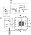
- FIG. 5 is a circuit diagram illustrating an oscillation circuit using an ultraviolet sensor according to an embodiment of the present invention.
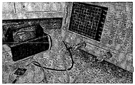
- FIG. 6 is a diagram of a system capable of measuring a frequency change according to an embodiment of the present invention.
- FIG. 1 is a view showing the configuration of an ultraviolet sensor according to an embodiment of the present invention.
- the ultraviolet sensor 100 includes a sensing film 110, an acoustic wave input unit 120, an acoustic wave output unit 130, and a piezoelectric material 140.
- the sensing layer 110 may correspond to a material disposed on the piezoelectric material 140 to sense ultraviolet rays, and the material may react with ultraviolet rays to change its characteristics.
- the sensing layer 110 may be implemented through zinc oxide (ZnO) nanoparticles, and the absorption rate of the zinc oxide (ZnO) nanoparticles will be described with reference to FIG. 4.
- the sensing layer 110 may be formed by spin coating zinc oxide (ZnO) nanoparticles on the elastic wave input unit 120, the elastic wave output unit 130, and the piezoelectric material 140.
- the sensing film 110 may anneal the spin-coated sensing film to improve electrical or mechanical properties.
- the elastic wave input unit 120 is disposed on one end of the sensing layer 110 on the piezoelectric material 140.
- the acoustic wave input unit 120 may be disposed to face the acoustic wave output unit 130 with respect to the sensing film 110.
- the elastic wave input unit 120 may receive an external electrical signal to form an electric field, and the piezoelectric material 140 may generate mechanical vibration (ie, elastic wave) through the formed electric field.
- the acoustic wave input unit 120 may provide the sensing film 110 with the acoustic wave generated based on an external electrical signal.
- the acoustic wave input unit 120 may be implemented as an interdigital transducer (IDT) formed through aluminum (Al) deposition.
- the interdigital converter can efficiently generate the elastic waves and propagate the acoustic waves along a solid surface (eg, between the sensing film 110 and the piezoelectric material 140).
- the acoustic wave input unit 120 may be implemented by disposing a metal electrode on the piezoelectric material 140, and may convert an electrical signal into an acoustic wave.
- the acoustic wave input unit 120 may be implemented in a grid structure.
- the lattice structure refers to a structure in which the horizontal and the vertical cross at right angles at intervals.
- the elastic wave output unit 130 is disposed on the other end of the sensing layer 110 on the piezoelectric material 140.
- the elastic wave output unit 130 may be disposed to face the acoustic wave input 120 around the sensing layer 110.
- the elastic wave output unit 130 may generate an electrical signal when mechanical vibration (ie, elastic wave) generated by the elastic wave input unit 120 is applied.
- the acoustic wave output unit 130 may generate an electrical signal based on the elastic wave provided by the elastic wave input unit 120 to detect a change in frequency of the generated electrical signal.
- the acoustic wave output unit 130 may be implemented as an interdigital converter formed through aluminum (Al) deposition.
- the interdigital converter can efficiently detect the elastic waves propagated along the solid surface (eg, between the sensing film 110 and the piezoelectric material 140).
- the elastic wave output unit 130 may be implemented by disposing a metal electrode on the piezoelectric material 140 and serves as a filter for filtering a frequency of a predetermined band in the process of converting the propagated elastic wave into an electrical signal. Perform.
- the acoustic wave output unit 130 may be implemented in a lattice structure on the piezoelectric material 140.
- the lattice structure refers to a structure in which the horizontal and the vertical cross at right angles at intervals.
- the piezoelectric material 140 may generate an electrical signal (eg, an acoustic wave) by receiving an electrical signal, and generate an electrical signal (eg, a voltage) by applying mechanical vibration to the piezoelectric body.
- the piezoelectric material 140 may include a piezoelectric substrate (eg, a semiconductor substrate) or a piezoelectric thin film.
- a specific frequency band of mechanical vibration may be used as a reference signal source of the ultraviolet sensor 100. That is, the piezoelectric material 140 may generate mechanical vibration (ie, acoustic wave) when an electrical signal is applied through piezoelectric and reverse piezoelectric effects, and may generate an electrical signal when mechanical vibration is applied.
- FIG. 2 is a view for explaining a UV sensor manufacturing method according to another embodiment of the present invention.
- the piezoelectric material 140 may be patterned through the photoresist 222 to generate the pattern 220.
- the pattern 220 may form irregularities in terms of the cross section of the piezoelectric material 140, and includes a photosensitive region (ie, protruding region) 222 and a non-photosensitive region (ie, recessed region) 224. can do.
- the non-photosensitive region (ie, the recessed region) 224 is left on the piezoelectric material 140, and the photosensitive region (ie, the protruding region) 222 can be removed.
- PhotoResist may cause chemical reactions when irradiated with light, and may correspond to AZ5214 photoresist.
- the non-photosensitive region 224 may be implemented in a grating structure to form an IDT.
- the piezoelectric material 210 having the pattern formed thereon may be deposited as a thin film 226.
- the deposition may grow a thin film through a chemical vapor deposition (CVD) process.
- the deposition may grow the thin film through a low pressure CVD, plasma enhanced CVD or atmospheric pressure CVD process.
- the thin film may use aluminum (Al). This is because aluminum has excellent malleability and ductility and good electrical conductivity.
- the thin film 226 may use an oxide or a nitride.
- the photoresist 222 and the thin film 226 deposited on the photoresist 222 may be removed by stripping the photoresist region 222. More specifically, the photoresist 222 and the thin film 226 remaining on the piezoelectric material 230 on which aluminum is deposited may be removed through alkali chemicals.
- the photosensitive region 222 refers to a region in which the piezoelectric material 140 is patterned through the photosensitive liquid
- the non-photosensitive region 224 refers to a region except for the photosensitive region 222.
- the non-photosensitive region 224 may be implemented in a lattice structure on the piezoelectric material 240 to form an interdigital converter.
- the interdigital converter can be implemented via aluminum (Al) deposited on the non-photosensitive region 224.
- the piezoelectric material 240 from which the photoresist 222 and the deposited thin film 226 are removed may be spin-coated through zinc oxide (ZnO) nanoparticles. More specifically, the piezoelectric material 240 from which the photoresist 222 and the deposited thin film 226 are removed may be rotated at high speed when the zinc oxide nanoparticles are introduced. As a result, the zinc oxide nanoparticles may spread thinly on the piezoelectric material 240.
- ZnO zinc oxide
- the sensing film 250 on the spincoated piezoelectric material may be annealed. More specifically, the spin-coated sensing film 250 may be heated to a temperature of 200 ° C. or more for about 1 hour to remove the damage of the spin-coated sensing film 250. When the spin-coated sensing layer 250 is annealed, electrical or mechanical properties may be improved.
- ⁇ v change in propagation velocity of a seismic wave
- FIG. 3A is a diagram showing a device manufactured by the ultraviolet sensor manufacturing method shown in FIG. 2.
- the manufactured device 300 includes a sensing film 310, an acoustic wave input unit 320, and an acoustic wave output unit 330.
- the sensing layer 310 may be implemented through zinc oxide nanoparticles.
- the acoustic wave input unit 320 and the acoustic wave output unit 330 may be implemented as an interdigital converter formed through aluminum deposition.
- FIG. 3B is a diagram illustrating an image captured by an optical camera of a sensing film manufactured by the UV sensor manufacturing method of FIG. 2.
- the sensing layer 310 may be formed by spin coating zinc oxide nanoparticles.
- the particles have a lower process cost than the thin film, and due to the nature of the particles themselves, the surface area (that is, the exposed area) is wide, and thus can react to more ultraviolet rays. As a result, the sensitivity of the sensing layer 310 can be improved.
- ZnO 4 is a graph showing the absorption rate according to the wavelength of zinc oxide (ZnO) nanoparticles.
- the x and y axes each represent a wavelength and an absorbance.
- the measured absorptivity can exhibit high absorptance only at wavelengths of 400 nm or less.
- zinc oxide nanoparticles exhibit an absorption greater than 80% at wavelengths of 400 nm or less. Since the wavelength of ultraviolet rays is between 100 nm and 380 nm, it can be seen that the ultraviolet absorption of the zinc oxide nanoparticles is high.
- FIG. 5 is a circuit diagram illustrating an oscillation circuit using an ultraviolet sensor according to an embodiment of the present invention.
- the oscillation circuit 500 may drive the acoustic wave using the ultraviolet sensor 510. More specifically, when an electrical signal is applied to the elastic wave input unit 520 through the oscillation circuit 500, the elastic wave input unit 520 may form an electric field through the received electrical signal.
- the piezoelectric material 140 generates elastic waves through the formed electric field, and the generated elastic waves propagate to the elastic wave output unit 530 through the sensing film.
- the elastic wave output unit 530 may form an electrical signal through the propagated elastic wave.
- the insertion loss of the sensing film in the oscillation circuit 500 may be measured based on the electrical signal formed in the acoustic wave output unit 530.
- the frequency change of the acoustic wave may be measured according to the insertion loss of the sensing layer 110. The method of measuring insertion loss and the gain obtained by measuring the frequency change of the acoustic wave will be described later.
- FIG. 6 is a diagram of a system capable of measuring a frequency change according to an embodiment of the present invention.
- the frequency change of the acoustic wave may be measured by the system when the ultraviolet sensor absorbs ultraviolet rays. More specifically, the center frequency may be measured based on the result of measuring insertion loss when no ultraviolet light is applied. Subsequently, when the ultraviolet light is applied, a system for measuring the frequency change of the ultraviolet light may change the center frequency when the ultraviolet light intensity is changed.
- each of the x and y axes represents a frequency and an insertion loss. More specifically, the center frequency (ie, the highest gain region) may be measured based on the result of measuring the insertion loss of the acoustic wave when ultraviolet rays are not applied. That is, the frequency response characteristic of the sensing layer 110 may be measured.
- the insertion loss refers to the internal loss generated on the operating frequency band while the acoustic wave passes through the sensing film 110. That is, the insertion loss refers to a loss generated when the acoustic wave generated based on the electrical signal passes through the sensing film 110. Therefore, the operation of the ultraviolet light can be determined by measuring the change in the center frequency through the insertion loss.
- the x-axis represents the intensity of ultraviolet rays and the y-axis represents frequency and phase, respectively. More specifically, the center frequency (ie, the highest gain region) may be measured based on the result of measuring the insertion loss of the acoustic wave according to the intensity of the ultraviolet light when the ultraviolet light is applied.
- the measured center frequency may represent a form proportional to the intensity of ultraviolet rays.
- the ultraviolet sensor Since a change in frequency can be measured when ultraviolet light is applied, the ultraviolet sensor can be operated even when a trace amount of ultraviolet light is detected. Therefore, since the ultraviolet sensor does not require the advancement of a specific circuit, price competitiveness can be secured.
- the present invention relates to an ultraviolet sensor that can measure the intensity of ultraviolet light by detecting a change in frequency, and a method of manufacturing the same, which has industrial applicability.
Landscapes
- Physics & Mathematics (AREA)
- General Physics & Mathematics (AREA)
- Spectroscopy & Molecular Physics (AREA)
- Acoustics & Sound (AREA)
- Engineering & Computer Science (AREA)
- Power Engineering (AREA)
- Photometry And Measurement Of Optical Pulse Characteristics (AREA)
- Light Receiving Elements (AREA)
Abstract
L'invention concerne un capteur d'ultraviolets comprenant : un matériau piézoélectrique ; un film de détection, disposé sur le matériau piézoélectrique, pour détecter des rayons ultraviolets ; une unité d'entrée d'ondes élastiques, agencée sur le matériau piézoélectrique, sur une extrémité du film de détection, pour fournir, à ce film de détection, des ondes élastiques générées sur la base de signaux électriques ; et une unité de sortie d'ondes élastiques, agencée sur le matériau piézoélectrique, sur l'autre extrémité du film de détection, pour détecter le changement de fréquence des signaux électriques générés sur la base des ondes élastiques. Par conséquent, étant donné que le capteur d'ultraviolets peut répondre à un plus grand nombre de rayons ultraviolets du fait que la superficie est plus grande en raison des caractéristiques de la particule elle-même, la sensibilité du capteur peut être améliorée, et du fait que le changement de fréquence de l'onde élastique est mesuré au moyen de nanoparticules d'oxyde de zinc (ZnO), la rentabilité peut être assurée.
Priority Applications (2)
| Application Number | Priority Date | Filing Date | Title |
|---|---|---|---|
| PCT/KR2015/007464 WO2017014328A1 (fr) | 2015-07-17 | 2015-07-17 | Capteur d'ultraviolets et son procédé de production |
| US15/873,803 US10222257B2 (en) | 2015-07-17 | 2018-01-17 | Oscillation circuit including an ultraviolet sensor |
Applications Claiming Priority (1)
| Application Number | Priority Date | Filing Date | Title |
|---|---|---|---|
| PCT/KR2015/007464 WO2017014328A1 (fr) | 2015-07-17 | 2015-07-17 | Capteur d'ultraviolets et son procédé de production |
Related Child Applications (1)
| Application Number | Title | Priority Date | Filing Date |
|---|---|---|---|
| US15/873,803 Continuation US10222257B2 (en) | 2015-07-17 | 2018-01-17 | Oscillation circuit including an ultraviolet sensor |
Publications (1)
| Publication Number | Publication Date |
|---|---|
| WO2017014328A1 true WO2017014328A1 (fr) | 2017-01-26 |
Family
ID=57834503
Family Applications (1)
| Application Number | Title | Priority Date | Filing Date |
|---|---|---|---|
| PCT/KR2015/007464 Ceased WO2017014328A1 (fr) | 2015-07-17 | 2015-07-17 | Capteur d'ultraviolets et son procédé de production |
Country Status (2)
| Country | Link |
|---|---|
| US (1) | US10222257B2 (fr) |
| WO (1) | WO2017014328A1 (fr) |
Families Citing this family (1)
| Publication number | Priority date | Publication date | Assignee | Title |
|---|---|---|---|---|
| KR102079659B1 (ko) * | 2018-04-05 | 2020-02-20 | 해성디에스 주식회사 | 광 센서 소자 및 이를 포함하는 광 센서 패키지 |
Citations (5)
| Publication number | Priority date | Publication date | Assignee | Title |
|---|---|---|---|---|
| JPH09243618A (ja) * | 1996-03-13 | 1997-09-19 | Kanagawa Kagaku Gijutsu Akad | センサ及びその製造方法 |
| US20030201694A1 (en) * | 2000-07-13 | 2003-10-30 | Rutgers, The State University Of New Jersey | Integrated tunable surface acoustic wave technology and sensors provided thereby |
| US20050116263A1 (en) * | 2002-06-06 | 2005-06-02 | Rutgers, The State University of New Jersey and | Multifunctional biosensor based on zno nanostructures |
| US20060024813A1 (en) * | 2004-05-21 | 2006-02-02 | Atonomics A/S | Nano-mechanic microsensors and methods for detecting target analytes |
| US20090289395A1 (en) * | 2008-05-21 | 2009-11-26 | Hon Hai Precision Industry Co., Ltd. | Method for manufacturing surface acoustic wave device |
Family Cites Families (3)
| Publication number | Priority date | Publication date | Assignee | Title |
|---|---|---|---|---|
| US5656414A (en) * | 1993-04-23 | 1997-08-12 | Fujitsu Limited | Methods of forming tall, high-aspect ratio vias and trenches in photo-imageable materials, photoresist materials, and the like |
| US20090064894A1 (en) * | 2007-09-05 | 2009-03-12 | Ashland Licensing And Intellectual Property Llc | Water based hydrophobic self-cleaning coating compositions |
| US9905610B2 (en) * | 2014-12-30 | 2018-02-27 | Win Semiconductors Corp. | Integrated structures of acoustic wave device and varactor, and acoustic wave device, varactor and power amplifier, and fabrication methods thereof |
-
2015
- 2015-07-17 WO PCT/KR2015/007464 patent/WO2017014328A1/fr not_active Ceased
-
2018
- 2018-01-17 US US15/873,803 patent/US10222257B2/en active Active
Patent Citations (5)
| Publication number | Priority date | Publication date | Assignee | Title |
|---|---|---|---|---|
| JPH09243618A (ja) * | 1996-03-13 | 1997-09-19 | Kanagawa Kagaku Gijutsu Akad | センサ及びその製造方法 |
| US20030201694A1 (en) * | 2000-07-13 | 2003-10-30 | Rutgers, The State University Of New Jersey | Integrated tunable surface acoustic wave technology and sensors provided thereby |
| US20050116263A1 (en) * | 2002-06-06 | 2005-06-02 | Rutgers, The State University of New Jersey and | Multifunctional biosensor based on zno nanostructures |
| US20060024813A1 (en) * | 2004-05-21 | 2006-02-02 | Atonomics A/S | Nano-mechanic microsensors and methods for detecting target analytes |
| US20090289395A1 (en) * | 2008-05-21 | 2009-11-26 | Hon Hai Precision Industry Co., Ltd. | Method for manufacturing surface acoustic wave device |
Also Published As
| Publication number | Publication date |
|---|---|
| US10222257B2 (en) | 2019-03-05 |
| US20180143069A1 (en) | 2018-05-24 |
Similar Documents
| Publication | Publication Date | Title |
|---|---|---|
| US5500534A (en) | Integrated energy-sensitive and position-sensitive x-ray detection system | |
| CN106796739B (zh) | 生成随机数的方法及相关的随机数生成器 | |
| Ng et al. | Considerations for an 8-inch wafer-level CMOS compatible AlN pyroelectric 5–14 μm wavelength IR detector towards miniature integrated photonics gas sensors | |
| WO2019052037A1 (fr) | Capteur capacitif et son procédé de fabrication | |
| JP2005229078A (ja) | 紫外線センサ及びその製造方法 | |
| CN103336053B (zh) | 一种独用参比的声表面波气体传感器阵列 | |
| CN108198897A (zh) | 一种石墨烯场效应晶体管量子点光电探测器及其制备方法 | |
| CN109244158A (zh) | 一种氧化镓场效应晶体管日盲探测器及其制作工艺 | |
| WO2017014328A1 (fr) | Capteur d'ultraviolets et son procédé de production | |
| CN111239792B (zh) | 一种侧窗式穿越辐射气体探测器 | |
| WO2017014329A1 (fr) | Capteur de lumière multiple et son procédé de production | |
| KR101847389B1 (ko) | 자외선 센서를 포함하는 발진회로 | |
| WO2016204378A1 (fr) | Détecteur de rayonnement et son procédé de fabrication | |
| CN105244404B (zh) | 集成光电传感器 | |
| WO2015150765A1 (fr) | Détection de lumière ultraviolette | |
| WO2012018162A1 (fr) | Dispositif de diagnostic du pouls utilisant un capteur optique | |
| KR101661113B1 (ko) | 다중 광 센서 및 이를 제조하는 방법 | |
| Kobayash et al. | Dynamic strain distribution sensor sheet based on ultra-thin PZT/SI array on flexible substrate for bridge monitoring wireless sensor network | |
| JP3768162B2 (ja) | 半導体処理装置とウエハセンサモジュール | |
| WO2023080375A1 (fr) | Interconnexion verticale appropriée pour un procédé de fabrication de mems comprenant un procédé à haute température, et son procédé de fabrication | |
| CN216930018U (zh) | 一种单触发纳秒脉冲检测终端 | |
| EP3841622A1 (fr) | Procédé de fabrication de capteurs ultrasonores | |
| Hatfield et al. | The use of integrated circuits for position-sensitive detection | |
| CN118632609A (zh) | 一种基于LiTaO3薄膜的热释电探头及其制备方法 | |
| CN121559247A (zh) | 一种基于二氧化铪薄膜的日盲紫外表面声波传感器及制造方法、局部放电检测系统 |
Legal Events
| Date | Code | Title | Description |
|---|---|---|---|
| 121 | Ep: the epo has been informed by wipo that ep was designated in this application |
Ref document number: 15898976 Country of ref document: EP Kind code of ref document: A1 |
|
| NENP | Non-entry into the national phase |
Ref country code: DE |
|
| 122 | Ep: pct application non-entry in european phase |
Ref document number: 15898976 Country of ref document: EP Kind code of ref document: A1 |