WO2017017859A1 - 光干渉計 - Google Patents
光干渉計 Download PDFInfo
- Publication number
- WO2017017859A1 WO2017017859A1 PCT/JP2015/075105 JP2015075105W WO2017017859A1 WO 2017017859 A1 WO2017017859 A1 WO 2017017859A1 JP 2015075105 W JP2015075105 W JP 2015075105W WO 2017017859 A1 WO2017017859 A1 WO 2017017859A1
- Authority
- WO
- WIPO (PCT)
- Prior art keywords
- light
- combined
- branched
- incident
- branching
- Prior art date
- Legal status (The legal status is an assumption and is not a legal conclusion. Google has not performed a legal analysis and makes no representation as to the accuracy of the status listed.)
- Ceased
Links
Images


Classifications
-
- G—PHYSICS
- G01—MEASURING; TESTING
- G01J—MEASUREMENT OF INTENSITY, VELOCITY, SPECTRAL CONTENT, POLARISATION, PHASE OR PULSE CHARACTERISTICS OF INFRARED, VISIBLE OR ULTRAVIOLET LIGHT; COLORIMETRY; RADIATION PYROMETRY
- G01J3/00—Spectrometry; Spectrophotometry; Monochromators; Measuring colours
- G01J3/28—Investigating the spectrum
- G01J3/45—Interferometric spectrometry
-
- G—PHYSICS
- G01—MEASURING; TESTING
- G01B—MEASURING LENGTH, THICKNESS OR SIMILAR LINEAR DIMENSIONS; MEASURING ANGLES; MEASURING AREAS; MEASURING IRREGULARITIES OF SURFACES OR CONTOURS
- G01B9/00—Measuring instruments characterised by the use of optical techniques
- G01B9/02—Interferometers
- G01B9/02015—Interferometers characterised by the beam path configuration
- G01B9/02017—Interferometers characterised by the beam path configuration with multiple interactions between the target object and light beams, e.g. beam reflections occurring from different locations
-
- G—PHYSICS
- G01—MEASURING; TESTING
- G01B—MEASURING LENGTH, THICKNESS OR SIMILAR LINEAR DIMENSIONS; MEASURING ANGLES; MEASURING AREAS; MEASURING IRREGULARITIES OF SURFACES OR CONTOURS
- G01B9/00—Measuring instruments characterised by the use of optical techniques
- G01B9/02—Interferometers
- G01B9/02015—Interferometers characterised by the beam path configuration
- G01B9/02022—Interferometers characterised by the beam path configuration contacting one object by grazing incidence
-
- G—PHYSICS
- G01—MEASURING; TESTING
- G01B—MEASURING LENGTH, THICKNESS OR SIMILAR LINEAR DIMENSIONS; MEASURING ANGLES; MEASURING AREAS; MEASURING IRREGULARITIES OF SURFACES OR CONTOURS
- G01B9/00—Measuring instruments characterised by the use of optical techniques
- G01B9/02—Interferometers
- G01B9/02041—Interferometers characterised by particular imaging or detection techniques
- G01B9/02044—Imaging in the frequency domain, e.g. by using a spectrometer
-
- G—PHYSICS
- G01—MEASURING; TESTING
- G01B—MEASURING LENGTH, THICKNESS OR SIMILAR LINEAR DIMENSIONS; MEASURING ANGLES; MEASURING AREAS; MEASURING IRREGULARITIES OF SURFACES OR CONTOURS
- G01B9/00—Measuring instruments characterised by the use of optical techniques
- G01B9/02—Interferometers
- G01B9/02055—Reduction or prevention of errors; Testing; Calibration
- G01B9/02056—Passive reduction of errors
- G01B9/02058—Passive reduction of errors by particular optical compensation or alignment elements, e.g. dispersion compensation
-
- G—PHYSICS
- G01—MEASURING; TESTING
- G01B—MEASURING LENGTH, THICKNESS OR SIMILAR LINEAR DIMENSIONS; MEASURING ANGLES; MEASURING AREAS; MEASURING IRREGULARITIES OF SURFACES OR CONTOURS
- G01B9/00—Measuring instruments characterised by the use of optical techniques
- G01B9/02—Interferometers
- G01B9/02055—Reduction or prevention of errors; Testing; Calibration
- G01B9/02056—Passive reduction of errors
- G01B9/02059—Reducing effect of parasitic reflections, e.g. cyclic errors
-
- G—PHYSICS
- G01—MEASURING; TESTING
- G01J—MEASUREMENT OF INTENSITY, VELOCITY, SPECTRAL CONTENT, POLARISATION, PHASE OR PULSE CHARACTERISTICS OF INFRARED, VISIBLE OR ULTRAVIOLET LIGHT; COLORIMETRY; RADIATION PYROMETRY
- G01J3/00—Spectrometry; Spectrophotometry; Monochromators; Measuring colours
- G01J3/28—Investigating the spectrum
- G01J3/45—Interferometric spectrometry
- G01J3/453—Interferometric spectrometry by correlation of the amplitudes
- G01J3/4532—Devices of compact or symmetric construction
Definitions
- the present invention relates to an optical interferometer.
- the optical interferometer described in Patent Document 1 uses, for example, a branching / multiplexing unit made of silicon, and reflects a part of incident light and transmits the remaining part on a certain plane of the branching / multiplexing unit. While branching into 1 branch light and 2nd branch light, these 1st branch light and 2nd branch light are combined, and it outputs as combined light. That is, in this optical interferometer, one plane of the branching / multiplexing unit includes a branching surface that splits the incident light into the first branching light and the second branching light, and the first branching light and the second branching light. It is commonly used as both of the multiplexing planes that combine and produce combined light.
- wavelength dispersion occurs while one of the first branched light and the second branched light reciprocates inside the branching / multiplexing unit, so that the other light is dispersed.
- the problem of chromatic dispersion is solved by reciprocating the inside of the compensation member.
- the optical interferometer described in Patent Document 2 uses a branching and combining unit made of, for example, silicon, and reflects a part of incident light on the first main surface of the branching and combining unit and transmits the remaining part to the first.
- the branched light and the second branched light are branched into two, and the first branched light and the second branched light are combined and output as the combined light on the second main surface of the branching / multiplexing unit. That is, in this optical interferometer, the incident light is branched into the first branched light and the second branched light, and the branched surface (first main surface) is combined with the first branched light and the second branched light.
- a combining surface (second main surface) to be combined light is separated.
- each of the first branch light and the second branch light passes through the inside of the branching / multiplexing unit only once, so that the problem of wavelength dispersion can be suppressed.
- the present invention has been made to solve the above problems, and an object thereof is to provide an optical interferometer capable of reducing the ratio of excess loss.
- the optical interferometer according to the present invention includes a branching and multiplexing unit, a first optical system, a second optical system, and a driving unit.
- the branching / combining part has a branching surface, an incident surface, a first exit surface, a combining surface, and a second exit surface at the boundary between the inside and the outside of the transparent member, and the branching surface and the combining surface are separate.
- the branch surface a part of incident light incident from the outside is reflected and emitted as the first branched light, and the remaining portion is transmitted as the second branched light to the inside.
- the first branched light that has entered through the optical system is transmitted to the inside, the second outgoing light that has reached from the branched surface through the inside is emitted to the outside at the first outgoing surface, and the combined surface from the incident surface through the inside at the first outgoing surface.
- the first branched light that has reached and the second branched light that has entered from the first emission surface via the second optical system a part of each is combined and emitted to the outside as the first combined light. Are combined and propagated as second combined light to the second output. In the surface, emitting the portion of the second multiplexed light arriving through the interior from the combining surface to the outside.
- the first optical system reflects the first branched light emitted from the branch surface by a mirror and enters the incident surface.
- the second optical system reflects the second branched light emitted from the first exit surface by a mirror and enters the combined surface.
- the driving unit adjusts a difference in optical path length between the first branched light and the second branched light from the branch surface to the combined surface by moving either the mirror of the first optical system or the second optical system.
- an optical interferometer capable of reducing the ratio of excess loss can be provided.
- FIG. 1 is a diagram showing a configuration of an optical interferometer 2A of the first comparative example.
- FIG. 2 is a diagram showing the configuration of the optical interferometer 2B of the second comparative example.
- FIG. 3 is a diagram showing an interferogram when white light is incident on the optical interferometer.
- FIG. 4 is a diagram showing an interferogram when white light is incident on the optical interferometer.
- FIG. 5 is a diagram illustrating the configuration of the optical interferometer 1A according to the first embodiment.
- FIG. 6 is a diagram showing the configuration of the optical interferometer 2C of the third comparative example.
- FIG. 7 is a diagram showing a configuration of an optical interferometer 2D of the fourth comparative example.
- FIG. 1 is a diagram showing a configuration of an optical interferometer 2A of the first comparative example.
- FIG. 2 is a diagram showing the configuration of the optical interferometer 2B of the second comparative example.
- FIG. 3 is a diagram showing an inter
- FIG. 8 is a graph showing the relationship between the refractive index of the material constituting the branching and combining unit 10 and the average interference intensity peak.
- FIG. 9 is a diagram illustrating an interferogram of the combined lights L 3 and L 41 .
- FIG. 10 is a diagram illustrating a difference in interferogram between the combined lights L 3 and L 41 .
- FIG. 11 is a circuit diagram of the detection unit 50 of the optical interferometer 1A of the first embodiment.
- FIG. 12 is a diagram illustrating a configuration of an optical interferometer 1B according to the second embodiment.
- FIG. 13 is a circuit diagram of the detection unit 50 of the optical interferometer 1B of the second embodiment.
- FIG. 14 is a diagram illustrating a configuration of an optical interferometer 1C according to the third embodiment.
- FIG. 1 is a diagram showing a configuration of an optical interferometer 2A of the first comparative example.
- the optical interferometer 2 ⁇ / b> A includes a branching / multiplexing unit 10, a mirror 21, a mirror 31, and a dispersion compensation member 90.
- the branching / multiplexing unit 10 is made of, for example, silicon and has a first main surface 10a and a second main surface 10b that are parallel to each other. A part of the incident light L 0 incident on the first main surface 10 a from the outside is reflected as the first branched light L 11 , and the remaining part is transmitted as the second branched light L 21 to the inside of the branching / multiplexing unit 10.
- the first branched light L 11 from the first major surface 10 a passes through the dispersion compensation member 90 and is reflected by the mirror 21.
- the first branched light L 12 reflected by the mirror 21 passes through the dispersion compensation member 90 again, enters the first main surface 10 a, and passes through the branch multiplexing unit 10.
- the second branched light L 21 from the first main surface 10 a passes through the inside of the branching and combining unit 10, passes through the second main surface 10 b, is emitted to the outside, and is reflected by the mirror 31.
- the second branched light L 22 reflected by the mirror 31 enters the second main surface 10b, passes through the inside of the branching / combining unit 10, passes through the inside of the branching / combining unit 10 again, and passes through the first main light 10b. Reflected by the surface 10a.
- the first branched light L 12 transmitted to the inside of the branching / combining unit 10 on the first main surface 10a and the second branched light L 22 reflected on the first main surface 10a are combined and combined light L 3. It becomes.
- the combined beam L 3 is passed through the inside of the branch multiplexing part 10, and is emitted to the outside through the second major surface 10b.
- the combined light L 3 emitted to the outside is detected by the detection unit 50.
- the first major surface 10a of the branch multiplexing section 10 branches the incident light L 0 into the first branched light L 11 and the second branch light L 21, and the first It is used as both of the combined surfaces of the branched light L 12 and the second branched light L 22 to be combined light L 3 .
- the position of the mirror 21 is fixed, and the mirror 31 can be moved by the drive unit along the incident direction of the second branched light L 21 .
- This driving unit can also be constituted by MEMS. Since the mirror 31 is movable, the optical path length difference between the first branched light and the second branched light can be adjusted.
- the branching and combining unit 10 and the dispersion compensating member 90 are made of the same material (for example, silicon). Further, the optical path length of the section in which the first branched lights L 11 and L 12 reciprocate inside the dispersion compensating member 90 and the section of the section in which the second branched lights L 21 and L 22 reciprocate inside the branch multiplexing unit 10 are obtained. The optical path lengths are set equal to each other. Thereby, the problem of wavelength dispersion is solved, and the wavelength dependency of the optical path length difference between the first branched light and the second branched light is reduced.
- the optical interferometer 2A When the optical interferometer 2A is used in an infrared spectrometer such as FTIR (Fourier Transform Infrared Spectroscopy), if the branching and combining unit 10 is made of quartz glass, the optical interferometer 2A is It can be used only in the near infrared region. Further, since the refractive index of quartz glass is not high, it is necessary to form a dielectric multilayer film for adjusting the branching ratio on the surface of quartz glass. Although it is conceivable to use the branching / multiplexing unit 10 made of an appropriate material according to the wavelength range, it is necessary to replace the branching / multiplexing unit 10 according to the wavelength range and perform optical adjustment, which is inconvenient. is there. Further, in the optical interferometer created by the MEMS technology, the branching / multiplexing unit 10 cannot be freely selected.
- FTIR Fastier Transform Infrared Spectroscopy
- the branching and combining unit 10 is made of a semiconductor material such as silicon from the viewpoint of suppressing such a problem. Since the refractive index of silicon is around 3.5 in the near-infrared region, when near-infrared light is perpendicularly incident on the interface between silicon and air, Fresnel reflection occurs due to the refractive index difference between the two media. The reflectivity is about 30%. That is, even if a dielectric multilayer film for adjusting the branching ratio is not provided on the surface of the branching and multiplexing unit 10 made of silicon, the silicon boundary surface itself becomes a branching surface having an appropriate branching ratio.
- silicon functions as a transparent medium up to the far-infrared region (several tens of ⁇ m or more), it is not necessary to strictly control the thickness.
- silicon has a large absorption in the wavelength region of 1.1 ⁇ m or less
- the target is the infrared region of 1.1 ⁇ m or more.
- germanium may be used in the near infrared region of 1 ⁇ m or less. Germanium can only be used up to about 5 ⁇ m in the mid-infrared region, but has a refractive index of about 4.0, and therefore has better branching characteristics than silicon.
- the branching / multiplexing unit 10 is made of a semiconductor material such as silicon or germanium, so that broadband light can be branched and multiplexed.
- the optical interferometer 2A an excess loss of light occurs in addition to the loss of light unavoidable in principle at the time of branching and multiplexing. This problem will be described below.
- first branch light L 12 is transmitted and reflected light to the interior, which occurs when incident on the first major surface 10a that is reflected by the mirror 21, although the transmitted light contributes to the interference, the reflected light contribute to the interference Because it does not, it becomes a loss. However, this is unavoidable for multiplexing, and this reflected light is inevitable in principle.
- the reflected light and transmitted light generated when the second branched light L 22 reflected by the mirror 31 enters the first main surface 10a the reflected light contributes to interference, but the transmitted light contributes to interference. Because it does not, it becomes a loss. However, this is also unavoidable for multiplexing, and this transmitted light is inevitable in principle.
- the second branch light L 21 is generated in the second main surface 10b in toward the mirror 31 passes through the second major surface 10b is not a loss of principle unavoidable, the excess loss.
- the second branch light L 22 is reflected light generated in the second main surface 10b in toward the first major surface 10a passes through the second main surface 10b is also loss of principle unavoidable reflected by the mirror 31 It is not an excess loss.
- the multiplexed light L 3 reflected light generated in the second main surface 10b when it is emitted to the outside through the second major surface 10b is also not in the loss of principle unavoidable, the excess loss.
- R be the power reflectivity at the time of Fresnel reflection of light on each of the first main surface 10a and the second main surface 10b of the branching and combining unit 10.
- the power transmittance is 1-R
- the branching ratio is R: (1-R).
- the reflectance and transmittance differ depending on the polarization direction and the incident angle of the incident light.
- S-polarized component of the incident light L 0 incident on the first major surface 10a remains S-polarized light component and beyond, P of the incident light L 0
- the polarization component remains the P polarization component thereafter.
- the first main surface 10a and the second main surface 10b is a parallel, if the incident angle is 45 degrees of the incident light L 0 to the first major surface 10a, or first major surface 10a from the outside
- the incident angles of light to the second main surface 10b are all 45 degrees, and the outgoing angles of light from the first main surface 10a or the second main surface 10b to the outside are all 45 degrees. Therefore, if attention is paid only to a specific polarization component, the reflectances R are all the same. Further, the reflectance of light at each of the mirrors 21 and 31 is 100%.
- the utilization efficiency I M1 of the light that reaches the detection unit 50 through the first branched light out of the incident light L 0 is expressed by the first main equation as shown in the following equation (1).
- the reflectance (R) at the surface 10a, the reflectance at the mirror 21 (1.0), the transmittance from the outside to the inside at the first main surface 10a (1-R), and the second main surface 10b Is calculated by the product of the transmittance (1-R) from the inside to the outside, and becomes R (1-R) 2 .
- the utilization efficiency I M2 of the light that reaches the detection unit 50 via the second branched light is the transmittance (1) from the outside to the inside of the first main surface 10a as shown in the following equation (2).
- -R the transmittance from the inside to the outside at the second principal surface 10b
- the reflectance at the mirror 31 1.0
- the transmittance from the outside to the inside at the second principal surface 10b (1-R)
- the reflectivity (R) at the first main surface 10a and the transmittance (1-R) from the inside to the outside at the second main surface 10b
- the interference intensity peak I pp of the combined light L 3 is expressed by the following equation (3).
- the branching and combining unit 10 is made of silicon, the refractive index of silicon at the target wavelength is 3.5, and the incident angle is 45 degrees, the reflectance R of the S-polarized component is about 43%, and the P-polarized component The reflectivity R is about 19%. Therefore, if the incident light L 0 is only the S-polarized component, the interference intensity peak I pp of the combined light L 3 is 15.9%. If the incident light L 0 is only the P-polarized component, the interference intensity peak I pp of the combined light L 3 is 20.2%. If the incident light L 0 is in an arbitrary polarization state, the interference intensity peak I pp of the combined light L 3 is a value between 15.9% and 20.2%.
- the incident light L 0 is incoherent light
- the incident light L 0 is considered that the polarization components in all directions are evenly distributed. Therefore, the interference intensity peak I pp of the combined light L 3 is The average value of S-polarized light and P-polarized light is 18.1%.
- the dispersion compensation member 90 In the case where the dispersion compensation member 90 is provided, if the light reflectance at the boundary surface of the dispersion compensation member 90 is R c and the transmittance is (1 ⁇ R c ), the first branch of the incident light L 0 is obtained.
- the utilization efficiency I M1 of light reaching the detection unit 50 via light is calculated as shown in the following equation (4).
- the interference intensity peak I pp of the combined light L 3 is expressed by the following equation (5). That is, by providing the dispersion compensation member 90, the interference intensity peak I pp of the combined light L 3 is reduced by the light transmittance (1-R c ) at the boundary surface of the dispersion compensation member 90. .
- the dispersion compensating member 90 Even when the dispersion compensating member 90 is provided, the same conditions as described above are applied to the branching and multiplexing unit 10, and light at the boundary surface of the dispersion compensating member 90 is assumed to be incident on the dispersion compensating member 90 vertically. Since the reflectance R c is 30% regardless of the polarization state, the interference intensity peak I pp of average of the combined light L 3 of the S polarized light and P-polarized light becomes 12.7%. Since it is necessary to provide a conventional FTIR Distributed compensating member 90, the 12.7% is the maximum value of the interference intensity peak I pp of the multiplexed light L 3.
- the utilization efficiency I M1 of the light that reaches the detection unit 50 via the first branched light in the incident light L 0 is as follows ( 6) Calculated as follows: Efficiency I M2 of light reaching the detector 50 via the second branched light of the incident light L 0 is the same.
- the interference intensity peak I pp of the combined light L 3 is expressed by the following equation (7).
- an anti-reflection (AR) coating to the second main surface 10b.
- AR anti-reflection
- the optical interferometer 2A is configured by a semiconductor process such as MEMS, it is difficult to selectively apply an AR coat to a specific surface of the branching / multiplexing unit 10, and in that case, an unavoidable loss. End up.
- FIG. 2 is a diagram showing a configuration of an optical interferometer 2B of the second comparative example.
- the optical interferometer 2 ⁇ / b> B includes a branching / multiplexing unit 10, a mirror 21, a mirror 31, and a mirror 32.
- the branching / multiplexing unit 10 is made of, for example, silicon and has a first main surface 10a and a second main surface 10b that are parallel to each other. A part of the incident light L 0 incident on the first main surface 10 a from the outside is reflected as the first branched light L 11 , and the remaining part is transmitted as the second branched light L 21 to the inside of the branching / multiplexing unit 10.
- the first branched light L 11 from the first major surface 10 a is reflected by the mirror 21.
- the first branch light L 12 that is reflected by the mirror 21 is incident on the first major surface 10a passes through the interior of the branch multiplexing section 10, it passes through the inside of the branch multiplexing section 10, the second main surface The light passes through 10b and is emitted to the outside.
- the second branched light L 21 from the first main surface 10a passes through the inside of the branching and combining unit 10, passes through the second main surface 10b, is emitted to the outside, is reflected by the mirror 31, and is reflected again by the mirror 32. Reflected.
- the second branched light L 22 reflected by the mirrors 31 and 32 enters the second main surface 10b and is reflected.
- the first branch light L 12 emitted to the outside by the second major surface 10b, and the second branch light L 22 that is reflected by the second major surface 10b is a combined light L 3 are multiplexed.
- the combined light L 3 is detected by the detection unit 50.
- the splitting surface of 2 branches the incident light L 0 into the first branched light L 11 and the second branch light L 21 (first principal surface 10a), a first branch light L 12 second the combining surface to be combined light L 3 multiplexes the branched light L 22 (second major surface 10b), there is a separate.
- the position of the mirror 21 is fixed, and the mirrors 31 and 32 can be moved by the drive unit along the incident direction of the second branched light L 21 .
- This driving unit can also be constituted by MEMS. Since the mirrors 31 and 32 are movable, the optical path length difference between the first branched light and the second branched light can be adjusted.
- each of the first branched light and the second branched light passes through the branching / multiplexing unit 10 only once, which is necessary for the optical interferometer 2A of the first comparative example.
- the problem of wavelength dispersion can be suppressed without using the dispersion compensating member 90.
- the optical interferometer 2B of the second comparative example has a smaller excess loss due to the boundary surface between the branching / combining unit 10 and the surrounding medium than the optical interferometer 2A of the first comparative example.
- Excess loss in the optical interferometer 2B of the second comparative example due to the reflected light by the second branch light L 21 is generated in the second main surface 10b when it is emitted to the outside through the second major surface 10b Only things.
- the utilization efficiency I M1 of the light that reaches the detection unit 50 via the first branched light, and the utilization efficiency I of the light that reaches the detection unit 50 via the second branched light of the incident light L 0 All of M2 are R (1-R) 2 .
- the interference intensity peak I pp of the combined light L 3 is expressed by the following equation (8). Also here, the incident angles of light from the outside to the first main surface 10a or the second main surface 10b are all 45 degrees.
- the branching and combining unit 10 is made of silicon
- the excess loss ratio in the case of the second comparative example is about half compared to the excess loss ratio of 68% in the case of the first comparative example.
- the optical interferometer 2B has the following problems.
- the branch surface (first main surface 10a) and the combining surface (second main surface 10b) are separate, the first branched light is reflected by one mirror 21.
- the second branched light is reflected by the two mirrors 31 and 32, and the first branched light and the second branched light are multiplexed at the multiplexing surface.
- the reflection position (combining position) of the second branched light on the second main surface 10b is from the inside to the outside on the second main surface 10b.
- light rays L 0R and L 0L passing through two different positions in the beam cross section of the incident light L 0 are considered.
- Two rays L 0R, L 0L of the incident light L 0 is propagated through different paths from each other in a plane parallel to both the incident direction of the normal and the incident light L 0 of the first main surface 10a.
- the first branch light L 11, L 12 a light beam from one of the light L 0R of the incident light L 0 and L 1R, the light beam from the other beam L 0L of the incident light L 0 and L 1L .
- the second branch light L 21, L 22 a light beam from one of the light L 0R of the incident light L 0 and L 2R, the light beam from the other beam L 0L of the incident light L 0 and L 2L .
- the light beams L2L of the second branched light are combined with each other. Further, the light beam L 1L of the first branch light from the other light beam L 0L of the incident light L 0, and the light L 2R in the second branch light from one of the light L 0R of the incident light L 0 is, each other It will be combined.
- the light beams of the first branched light and the second branched light that reach each position on the combined surface (second main surface 10b) are derived from different light beams in the incident light, they are combined with each other. Even if it becomes combined light, it does not become the original interference light.
- the incident light L 0 is given as a collimated light beam that spreads one light beam like a point light source, the light beams of the first branched light and the second branched light reaching each position interfere with each other.
- the spatial distance between the light beam L 1R and the light beam L 1L in the beam cross section of the first branched light generates an optical path length difference, the quality of the interference signal is degraded.
- the optical path length difference between the first branched light and the second branched light reaching each position is the same as the optical path length difference adjusted by the movement of the mirror.
- the optical path length difference is different between the one near the center and the one near the end, and the interference signals observed as a whole are averaged. It ’s weakened.
- optical interferometer used in FTIR
- light having a large beam diameter is used in order to improve parallelism of propagating light.
- the optical interferometer 2B using the combined light at different positions as an interference signal has an essential problem regarding interference.
- Patent document 1 discloses the invention of the optical interferometer comprised by MEMS in order to meet such a request
- the optical interferometer is miniaturized by MEMS, the interference efficiency in the optical interferometer is deteriorated, and there is a problem that visibility is deteriorated by stray light.
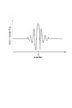
- 3 and 4 are diagrams showing interferograms when white light is incident on the optical interferometer.
- the horizontal axis represents the difference in optical path length between the first branched light and the second branched light from the branch plane to the combined plane.
- the vertical axis represents the intensity (interferogram) of the combined light L 3 (optical interference signal). Since the incident light is white light, the strongest interference is obtained when the optical path length difference is 0, and the interference becomes weaker as the absolute value of the optical path length difference increases.
- the average value of the optical interference signal is m and the difference between the maximum value and the minimum value of the optical interference signal is ⁇ , the visibility is expressed by ⁇ / (2 m).
- the ideal optical interferometer without stray light has a visibility value close to 1 (Fig. 3).
- the average value m of the optical interference signal increases, and the difference ⁇ between the local maximum value and the local minimum value of the optical interference signal decreases, so the visibility value decreases (FIG. 4).
- the visibility value decreases (FIG. 4).
- the light to be measured guided by an optical fiber having a core diameter of 400 ⁇ m and NA of 0.2 is emitted from the emission end of the optical fiber and incident on the optical interferometer, the following is considered. become.
- the spread of the light beam in the optical interferometer degrades the resolution, and the magnitude of the degradation is about 2 (1-cos (NA)) as the relative accuracy of the wave number.
- the beam of NA 0.2 is converted into a beam of NA 0.045, and the beam size after conversion is 0.2 / 0.00 of the beam size before conversion. It becomes as large as 1800 ⁇ m, which is 045 times. Actually, since it cannot be a perfect collimated light, it is preferable to configure an optical interferometer by using an optical system having a sufficiently large size with respect to the beam size.
- the average value m of the interferogram described above is increased.
- the degree of increase in the average value m of the interferogram depends on the size of the optical system and the optical interferometer.
- the average value m of the interferogram may be several to ten times the difference ⁇ between the maximum value and the minimum value of the optical interference signal.
- the influence of stray light can be removed by processing the signal output from the detection unit.
- the S / N of the signal output from the detection unit is deteriorated.
- the intensity of the interference light is small, the value of the output signal from the detector can be increased by increasing the gain of the amplifier included in the detector, but if the average value is large, the dynamic range of the amplifier Is used up by amplification of the average value signal.
- the inefficiency of the optical interferometer not only reduces the signal intensity of the original optical interference signal, but also increases the average value that uses up the dynamic range of the first-stage amplifier, resulting in signal acquisition.
- the S / N at the time is further deteriorated.
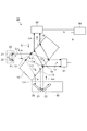
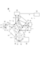
- FIG. 5 is a diagram showing a configuration of the optical interferometer 1A of the first embodiment.
- the optical interferometer 1 ⁇ / b> A includes a branching / multiplexing unit 10, a first optical system 20, a second optical system 30, and a driving unit 40. These components of the optical interferometer 1A are preferably constituted by MEMS.
- the branching / combining unit 10 is made of a semiconductor transparent member such as silicon, for example, and has a branch surface 11, an incident surface 12, a first exit surface 13, a combining surface 14, and a second at the boundary between the inside and the outside of the transparent member.
- An exit surface 15 is provided.
- the branching / multiplexing unit 10 reflects a part of the incident light L 0 incident from the outside on the branching surface 11 to be emitted as the first branched light L 11 , and transmits the remaining part as the second branched light L 21 to the inside.
- Branch multiplexing section 10 in the entrance surface 12, and transmits the first branched light L 12 incident through the first optical system 20 from the splitting surface 11 to the inside.
- the branching / combining unit 10 emits the second branched light L 21 that has reached from the branching surface 11 through the inside on the first emission surface 13 to the outside.
- the branching / multiplexing unit 10 includes a first branching light L 12 that has reached from the entrance surface 12 through the inside of the combining surface 14, and a second branching light L that has entered the first exit surface 13 through the second optical system 30. A part of each of 22 is combined and emitted as the first combined light L 3 to the outside, and the remaining parts are combined and propagated as the second combined light L 4 to the inside.
- the branching / combining unit 10 emits a part L 41 of the second combined light L 4 that has reached from the combining surface 14 through the inside at the second emitting surface 15 to the outside.
- the first optical system 20 reflects the first branched light L 11 emitted from the branch surface 11 by the mirrors 21 and 22, and causes the reflected first branched light L 12 to enter the incident surface 12.
- the second optical system 30, the second branch light L 21 emitted from the first emission face 13 is reflected by mirrors 31 and 32, is incident on the second branched light L 22 having its is reflected to combining surface 14.
- the drive unit 40 moves the mirror of either the first optical system 20 or the second optical system 30, and the optical path length difference between the first branched light and the second branched light from the branch surface 11 to the multiplexing surface 14 is determined. Adjust.
- each of the branch surface 11, the incident surface 12, the first exit surface 13, and the combining surface 14 of the branching and combining unit 10, and the incident position and the incident angle of light on each of these surfaces are the first branch on the combining surface 14.
- Set to The optical path lengths of the first branched light and the second branched light inside the branching / multiplexing unit 10 are equal to each other. Thereby, the problem of wavelength dispersion is solved, and the wavelength dependency of the optical path length difference between the first branched light and the second branched light is reduced.
- the branch surface 11 and the combining surface 14 are separate.
- the branch surface 11, the incident surface 12, and the second exit surface 15 may not be parallel to each other, may be parallel to each other, or may be on a common plane.
- the incident region of the incident light L 0 on the branch surface 11 and the incident region of the first branched light L 12 on the incident surface 12 may be different from each other, or a part or all of them may coincide with each other.
- the first emission surface 13 and the combining surface 14 may not be parallel to each other, may be parallel to each other, or may be on a common plane.
- the exit region of the second branched light L 21 on the first exit surface 13 and the exit region of the combined light on the combining surface 14 may be different from each other, or part or all may be coincident with each other.
- a part of the incident light L 0 incident on the branch surface 11 from the outside is reflected as the first branched light L 11 , and the remaining part is transmitted as the second branched light L 21 to the inside of the branching / multiplexing unit 10.
- the first branch light L 11 from the splitting surface 11 is reflected by mirrors 21, 22 of the first optical system 20.
- the reflected first branched light L 12 is incident on the incident surface 12, passes through the branching / multiplexing unit 10, passes through the branching / multiplexing unit 10, and reaches the multiplexing surface 14.
- the second branched light L 21 from the branch surface 11 passes through the inside of the branching / multiplexing unit 10, passes through the first emission surface 13, is emitted to the outside, and is reflected by the mirrors 31 and 32 of the second optical system 30. Is done.
- the reflected second branched light L 22 reaches the multiplexing surface 14.
- the component transmitted through the combining surface 14 in the first branched light L 12 reaching the combining surface 14 and the component reflected on the combining surface 14 in the second branched light L 22 reaching the combining surface 14 are combined. It is emitted to the outside as a first combined beam L 3 Te.
- the first combined light L 3 emitted from the combining surface 14 to the outside is received by the first light receiving element 51.
- the component reflected by the combining surface 14 in the first branched light L 12 reaching the combining surface 14 and the component transmitted through the combining surface 14 in the second branched light L 22 reaching the combining surface 14 are combined. It propagates to the interior as a second combined beam L 4 Te.
- the second combined light L 4 reaches the second emission surface 15, and a part L 41 thereof is emitted from the second emission surface 15 to the outside.
- the second combined light L 41 emitted from the second emission surface 15 to the outside is received by the second light receiving element 52.
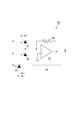
- the first light receiving element 51, the second light receiving element 52, and the current-voltage conversion unit 54 constitute a detection unit that detects an interference signal.
- the first light receiving element 51 receives the first combined beam L 3 emitted from the combining surface 14 to the outside, and outputs the first current signal I 1 in accordance with the amount of received light.
- the second light receiving element 52, the second combined light L 41 emitted to the outside from the second output surface 15 receives and outputs a second current signal I 2 in accordance with the amount of received light.
- the current-voltage converter 54 outputs a voltage signal corresponding to a value (I 1 -I 2 ) obtained by subtracting the second current signal I 2 from the first current signal I 1 . Details of the detection unit will be described later.
- the sum of the number of mirrors of the first optical system 20 and the number of mirrors of the second optical system 30 is an even number, light of each position in the beam cross section of the incident light L 0 Can be multiplexed at the common position in the beam cross section of the multiplexed light L 3 and L 4 at the multiplexing plane 14 after branching at the branch plane 11, so that the interference efficiency can be improved as compared with the configuration of the second comparative example. Can do.
- the optical interferometer 1A of the present embodiment is different from the configuration of the second comparative example, the first combined beam L 3 emitted from the combining surface 14 to the outside not only received by the first light receiving element 51,
- the second light receiving element 52 is also different in that the second combined light L 41 emitted from the second emission surface 15 to the outside is received by the second light receiving element 52.
- the optical interferometer 1A of the present embodiment can reduce the excess loss ratio as compared with the configuration of the second comparative example.
- the excess loss in this embodiment is calculated as follows.
- the interference intensity peak I pp of the first combined light L 3 emitted from the combining surface 14 and received by the first light receiving element 51 is expressed by the above equation (8).
- the interference intensity peak I pp of the second combined light L 41 emitted from the second emission surface 15 and received by the second light receiving element 52 is transmitted to the second light receiving element 52 via the first branched light in the incident light L 0.
- equation (11) is obtained.
- the total interference intensity peak I ppT is expressed as the sum of the expressions (8) and (11) as follows : (12)
- the branching and combining unit 10 is made of silicon
- FIG. 6 is a diagram showing the configuration of the optical interferometer 2C of the third comparative example.
- the incident light L 0 incident on the beam splitter 110 is branched into two by the beam splitter 110 into a first branched light L 1 as a reflection component and a second branched light L 2 as a transmission component.
- the first branched light L 1 is reflected by the mirror 120 and enters the beam splitter 110 again
- the second branched light L 2 is reflected by the mirror 130 and enters the beam splitter 110 again.
- the combined beam L 3 are multiplexed.
- the interference intensity peak I pp of the combined light L 3 is expressed by the following equation (13).
- the optical beam splitting ratio of the ideal beam splitter 110 that can maximize the interference intensity peak I pp in the optical interferometer 2C is 1: 1.
- FIG. 7 is a diagram showing a configuration of an optical interferometer 2D of the fourth comparative example.
- the optical interferometer 2D of the fourth comparative example shown in FIG. 7 is obtained by adding a beam splitter 111 to the configuration of the optical interferometer 2C of the third comparative example shown in FIG. Beam splitter 111 provided to detect the combined light L 4 are, is inserted into the optical path of the incident light L 0. Insertion of the beam splitter 111, loss occurs in the incident light L 0. As a result, if the optical branching ratio of each of the beam splitters 110 and 111 is 1: 1, the total interference intensity peak I pp of the combined lights L 3 and L 4 is 37.5%.
- the optical interferometer 2C having a general configuration in which both branching and multiplexing are performed by one beam splitter is ideal for obtaining a maximum efficiency of 50%, and this maximum efficiency of 50% is theoretically. It will be a limit.
- the reason why the principle limit can be exceeded by the configuration of the optical interferometer 1A of the present embodiment shown in FIG. 5 is that the branching surface 11 and the combining surface 14 are separate in the branching / combining unit 10, and The surface 11 and the combining surface 14 are arranged at a certain distance, and the second emitting surface 15 from which the second combined light L 41 is emitted and the branch surface 11 from which the incident light L 0 is incident are separated. It depends on being able to.
- the light reflectivity R at the beam splitter 110 is 50%.
- the ideal value of the light reflectance R on each surface is not 50%.
- the branching / multiplexing unit 10 is made of silicon, if light can be vertically incident on each surface, the reflectivity is 30%, so that an ideal beam splitter is obtained. However, in the actual design, since normal incidence cannot be achieved, comparison is made with an average interference intensity peak in consideration of the S-polarized component and the P-polarized component similar to those described above.
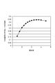
- FIG. 8 is a graph showing the relationship between the refractive index of the material constituting the branching and combining unit 10 and the average interference intensity peak.
- the calculation was performed by setting the incident angle of light from the outside to the branching and combining unit 10 to 45 degrees. From this calculation result, it can be seen that the average interference intensity peak has a maximum value of 44% when the refractive index is 3.5. Since the refractive index of silicon in the near-infrared region is 3.5, the optical interferometer 1A of the present embodiment that performs branching and multiplexing using the difference in refractive index between the material constituting the branching and multiplexing unit 10 and air. Then, it can be said that silicon is ideal as a material constituting the branching and multiplexing unit 10.
- a method is considered in which the first combined light L 3 and the second combined light L 41 are optically combined by some method and received by one photodetector.
- white light is only linearly added with continuous light, only light of one wavelength will be considered below.
- the angular frequency of light be ⁇ and the time variable be t.
- the electric field E 3 of the first combined light L 3 emitted from the combining surface 14 includes the electric field a 13 sin ( ⁇ t + ⁇ 13 ) of the first branched light reaching the combining surface 14 and the second branched light reaching the combining surface 14.
- the signal output from the square detector is a temporal average value of the square of the electric field E 3 of the first combined light L 3 (that is, the electric field). represents a square) amplitude a 3, it depends on the phase difference ( ⁇ 13 - ⁇ 23).
- the phase difference ( ⁇ 13 ⁇ 23 ) in the equation of the amplitude a 3 of the electric field E 3 of the first combined light L 3 is an optical path between the first branched light and the second branched light set by the drive unit. This corresponds to the length difference and is independent of the initial phase.
- the phase ⁇ 3 in the sin function related to the temporal change of the electric field E 3 of the first combined light L 3 depends on both the optical path length difference and the initial phase.
- the electric field E 4 of the second combined light L 41 emitted from the second emission surface 15 is applied to the electric field a 14 sin ( ⁇ t + ⁇ 14 ) of the first branched light reaching the second emission surface 15 and to the second emission surface 15.
- the sum of the electric field a 24 sin ( ⁇ t + ⁇ 24 ) of the reached second branched light is expressed by the following equations (16) and (17).
- phase change during the propagation of the second combined light from the combining surface 14 to the second emitting surface 15 is defined as ⁇ .
- the phase change ⁇ ⁇ depends on the angular frequency ⁇ .
- the phase difference ( ⁇ 14 ⁇ 24 ) in the equation of the amplitude a 4 of the electric field E 4 of the second combined light is the phase difference ( ⁇ 14 ⁇ 24 ) in the equation of the amplitude a 3 of the electric field E 3 of the first combined light ( equal to ⁇ 13 ⁇ 23 ).
- a first combined beam L 3 field E T for all the multiplexed light multiplexed by the second combined beam L 41 is an electric field E 3 of the first multiplexed light L 3 between the electric field E 4 of the second combined beam L 41
- the sum is expressed by the following formulas (20) and (21).
- the signal output from the photodetector that has received all the combined light has different values depending on the wavelength due to the influence of the phase ⁇ ⁇ that differs depending on the wavelength. That is, the interference signal changes due to a factor other than the optical path length difference between the first branched light and the second branched light, and does not function correctly as an optical interferometer.
- the first combined light L 3 and the second combined beam L 41 detected by separate photodetectors consider the method of adding the voltage signal after square detection by each of the photodetectors. In this way, since not appear the effect of the phase phi omega, the addition of the voltage signal as an interference signal to function properly.
- the photodetector typically includes an amplifier that amplifies the signal to a voltage level that is easy to process after output. When a photovoltaic light receiving element is used, the overall S / N is determined by the noise of the first-stage amplifier. When the first combined light L 3 and the second combined light L 41 are detected by separate photodetectors and signal amplification is performed, the total noise is twice that of the first-stage amplifier of each photodetector.
- the S / N is not improved.
- the efficiency of the first combined light L 3 is 26.4%
- the efficiency of the second combined light L 41 is 17.8%. In other words, the S / N will deteriorate.
- the first combined light L 3 and the second combined light L 41 are detected by separate light receiving elements, and a result obtained by adding and subtracting current signals output from the respective light receiving elements is converted into a voltage signal. think of. In this method, the above-described problem of S / N degradation can be avoided.
- the third detection method will be described, and the configuration of the detection unit 50 based on this method will be described.
- the phase may change.
- the amount of phase change when light is reflected at the boundary surface depends on the refractive index of each medium, the incident angle of light on the boundary surface, and the polarization state of the light. Assuming that each medium is a dielectric and the absorption coefficient can be ignored, the phase change occurs when light is reflected at the boundary surface.
- S-polarized light is incident on the boundary surface from the low refractive index medium side.
- P-polarized light is incident on the boundary surface from the high refractive index medium side at an incident angle equal to or less than the Brewster angle, and in each case, the phase change amount is ⁇ .
- the amount of phase change at the time of reflection of light in the configuration of the optical interferometer 1A shown in FIG. 5 will be considered.
- the phase of the first branched light L 12 and the second branched light L 22 incident on the multiplexing surface 14 is used as a reference, the S polarization component of the second branched light L 22 is reflected by the multiplexing surface 14 and the first combined light L 3.
- ⁇ phase change occurs, and when the P polarization component of the first branched light L 12 is reflected by the combining surface 14 to become the second combined light L 41 , a ⁇ phase change occurs.
- the second combined light L 41 emitted from the second emission surface 15 is different from the first combined light L 3 emitted from the synthesis surface 14 in terms of both the S-polarized component and the P-polarized component. ⁇ . That is, the signs of the interference signals of the first combined light L 3 and the second combined light L 41 are opposite to each other.
- the S-polarized component of the second branched light L 22 is reflected by the combining surface 14, a phase change of ⁇ occurs, and when the incident light L 0 is bifurcated by the branch surface 11, the first branch is generated.
- the phases of the S polarization components of the first branched light L 12 and the second branched light L 22 at the time of multiplexing are the same. Further, the phases of the P-polarized components of the first branched light L 12 and the second branched light L 22 at the time of multiplexing are also the same. After all, the signs of the interference signals of the S polarization component and the P polarization component are the same.
- each of the first optical system 20 and the second optical system 30 is a metal mirror
- a phase change occurs when light is reflected by the metal mirror. If the first optical system 20 and the second optical system 30 reflect light with a mirror having a common configuration, the same phase change occurs in both the S-polarized component and the P-polarized component.
- the signs of the interference signals are the same.
- the first combined beam L 3 and the second combined beam L 41 is the sign of the interference signal at all wavelengths become opposite to each other.
- FIG. 9 is a diagram illustrating an interferogram of the combined lights L 3 and L 41 .
- the interference signal of the first combined beam L 3 whereas the maximum value, the interference signal of the second combined beam L 41 is a minimum value.
- One of the interferogram of the first combined light L 3 and the interferogram of the second combined light L 41 is inverted up and down around the average value for the other interferogram, and the amplitude is corrected according to the efficiency. Is equivalent to
- the interferograms of the first combined light L 3 and the second combined light L 41 are displayed as having different average values.
- the average value of the interferogram depends on the configuration of the optical interferometer. For example, if more background light is incident on the photodetector than the non-interfering light from the optical interferometer and the average value of the interferogram is increased, the first combined light L 3 and the second combined light The difference between the average values of the L 41 interferograms is not so large.
- FIG. 10 is a diagram illustrating a difference in interferogram between the combined lights L 3 and L 41 .
- a part of the interference signal may have a negative value, but there is no problem in the circuit of the detection unit 50 shown in FIG.
- FIG. 11 is a circuit diagram of the detection unit 50 of the optical interferometer 1A of the first embodiment.
- the detection unit 50 includes a first light receiving element 51, a second light receiving element 52, and a current-voltage conversion unit 54.
- the current-voltage conversion unit 54 includes an amplifier 55 and a feedback resistor 56.
- the feedback resistor 56 is provided between the inverting input terminal of the amplifier 55 and the output terminal Vo.
- Each of the first light receiving element 51 and the second light receiving element 52 is a photovoltaic type, for example, a photodiode.
- the first light receiving element 51 and the second light receiving element 52 are connected in series between the first reference potential end V1 and the second reference potential end V2, and a reverse voltage is applied thereto.
- V1 is a positive potential and V2 is a negative potential.
- a connection point between the first light receiving element 51 and the second light receiving element 52 is connected to the inverting input terminal of the amplifier 55.
- the non-inverting input terminal of the amplifier 55 is connected to the ground potential terminal.
- the inverting input terminal that is in an imaginary short relationship with the non-inverting input terminal of the amplifier 55 also becomes the ground potential.
- the first light receiving element 51 receives the first combined beam L 3 emitted from the combining surface 14 to the outside, and outputs the first current signal I 1 in accordance with the amount of received light.
- the second light receiving element 52, the second combined light L 41 emitted to the outside from the second output surface 15 receives and outputs a second current signal I 2 in accordance with the amount of received light.
- a difference current (I 1 -I 2 ) between the first current signal I 1 and the second current signal I 2 flows to the feedback resistor 56, and is the product of the difference current value and the resistance value of the feedback resistor 56.
- a corresponding voltage value appears at the output terminal Vo. That is, the current-voltage converter 54 can output a voltage signal corresponding to a value (I 1 -I 2 ) obtained by subtracting the second current signal I 2 from the first current signal I 1 from the output terminal Vo.
- Voltage signal output from the output terminal Vo represents the difference interferogram of the respective first combined beam L 3 and the second combined beam L 41, while reducing the average value of the interferogram, emphasizing an interference signal It is a thing. Since the voltage signal output from the output terminal Vo is determined by only one amplifier 55, the S / N is improved. Further, by reducing the average value of the interferogram, the gain of the amplifier 55 can be appropriately set according to the magnitude of the interference signal.
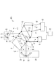
- FIG. 12 is a diagram showing a configuration of the optical interferometer 1B of the second embodiment.
- the optical interferometer 1 ⁇ / b> B includes a branching / multiplexing unit 10, a first optical system 20, a second optical system 30, and a driving unit 40. These components of the optical interferometer 1B are preferably constituted by MEMS.
- the branching / combining unit 10 is made of a semiconductor transparent member such as silicon, for example, and has a branch surface 11, an incident surface 12, a first exit surface 13, a combining surface 14, a second surface at the boundary between the inside and the outside of the transparent member. It has an emission surface 15 and a third emission surface 16.
- the optical interferometer 1B of the second embodiment shown in FIG. is different in having.
- the optical interferometer 1B of the second embodiment is one of the second combined light L 4 that is transmitted through the second emission surface 15 and emitted to the outside.
- the third light receiving element 53 also reflects the remaining portion L 42 of the second combined light L 4 that is reflected by the second emission surface 15, passes through the third emission surface 16 and is emitted to the outside. It differs in the point detected by.
- the second combined light L 42 emitted from the third emission surface 16 has only one more reflection than the second combined light L 41 emitted from the second emission surface 15. Accordingly, the interference intensity peak I pp2 of the second combined light L 42 emitted from the third emission surface 16 and received by the third light receiving element 53 is emitted from the second emission surface 15 and received by the second light receiving element 52. It becomes R times the interference intensity peak I pp1 of the second combined light L 41 , and is expressed by the following equation (22).
- the second combined light L emitted from the third emitting surface 16 and received by the third light receiving element 53 is used.
- the average interference intensity peak of 42 S-polarized light and P-polarized light is 5.3%.
- the average interference intensity peak of the S-polarized light and the P-polarized light combining the three combined lights L 3 , L 41 , and L 42 is 49.5%, and an efficiency of about 50% is obtained.
- the second combined light reflected by the third output surface 16 can be emitted from the other output surface to the outside and received by other light receiving elements, and when all of the second combined light L 4 is detected, overall efficiency of the second combined beam L 4 are a 26.4%.
- the total value of 52.8% of the efficiency 26.4% of the first combined light L 3 and the overall efficiency 26.4% of the second combined light L 4 is three depending on the configuration of the optical interferometer 1B in FIG. Compared with the efficiency of 49.5% when the combined lights L 3 , L 41 and L 42 are combined, the degree of improvement is small. Since the second combined light reflected by the third emission surface 16 is emitted from the other emission surface to the outside and received by the other light receiving elements, the configuration is complicated, but the degree of improvement is small. Absent.
- FIG. 13 is a circuit diagram of the detection unit 50 of the optical interferometer 1B of the second embodiment.
- the detection unit 50 includes a first light receiving element 51, a second light receiving element 52, a third light receiving element 53, and a current-voltage conversion unit 54.
- the detection unit 50 of the second embodiment shown in FIG. 13 is different in that it further includes a third light receiving element 53.
- the third light receiving element 53 is also of a photovoltaic type, for example, a photodiode.
- the phase change at the time of reflection of the second combined light L 42 emitted from the third emission surface 16 is the same as the phase change at the time of reflection of the second combined light L 41 emitted from the second emission surface 15. Therefore, the third light receiving element 53 that receives the second combined light L 42 emitted from the third emitting surface 16 is the second light receiving element that receives the second combined light L 41 emitted from the second emitting surface 15. 52 in parallel. The third light receiving element 53 receives the second combined light L 42 emitted from the third emission surface 16 to the outside, and outputs a third current signal I 3 corresponding to the amount of received light.
- the current-voltage converter 54 outputs a voltage signal according to a value (I 1 -I 2 -I 3 ) obtained by subtracting the second current signal I 2 and the third current signal I 3 from the first current signal I 1 as the output terminal Vo. Output from.
- the optical interferometer 1B of the second embodiment attention should be paid to the case where the background light is more incident than the non-interfering light from the optical interferometer and is incident on the photodetector to increase the average value of the interferogram. is necessary.
- the value obtained by subtracting the second current signal I 2 and the third current signal I 3 from the first current signal I 1 I In 1 -I 2 -I 3
- an average value component for one interferogram appears.
- the dynamic range may be narrowed by adding the third light receiving element 53.
- FIG. 14 is a diagram illustrating a configuration of an optical interferometer 1C according to the third embodiment.
- the optical interferometer 1 ⁇ / b> C includes a branching / multiplexing unit 10, a first optical system 20, a second optical system 30, and a driving unit 40. These components of the optical interferometer 1C are preferably constituted by MEMS.
- the branching / combining unit 10 is made of a semiconductor transparent member such as silicon, for example, and has a branch surface 11, an incident surface 12, a first exit surface 13, a combining surface 14, a second surface at the boundary between the inside and the outside of the transparent member. It has an exit surface 15 and a total reflection surface 17.
- the branching / combining unit 10 further includes a total reflection surface 17. It is different in point.
- the branching / combining unit 10 causes the total reflection surface 17 to totally reflect the second combined light L 4 that has arrived from the multiplexing surface 14 through the inside, and causes the second output light 15 to enter the second output surface 15.
- the second combined light L 4 can be totally reflected on the total reflection surface 17, that is, the incident angle of the second combined light L 4 on the total reflection surface 17 is equal to or greater than the critical angle.
- the orientation of the total reflection surface 17 is set. Further, the second combined light L 4 totally reflected by the total reflection surface 17 can be emitted from the second emission surface 15 to the outside, that is, the second combined light L 4 to the second emission surface 15 is emitted.
- the orientation of the second exit surface 15 is set so that the incident angle is less than the critical angle.
- the branch surface 11 on which the incident light L 0 is incident and the second output surface 15 from which the second combined light L 41 is output are provided on the common side with respect to the branching / combining unit 10. Therefore, there may be a limitation in the arrangement of the optical systems of the incident light L 0 and the second combined light L 41 .
- the branch surface 11 is provided on one side of the branching / combining unit 10, and the multiplexing surface 14 and the second emission surface 15 are provided on the other side of the branching / combining unit 10. since it is, the incident light L 0 and the multiplexed light L 3, L 41 is easily arranged in each optical system.
- optical interferometer according to the present invention is not limited to the above-described embodiments and configuration examples, and various modifications are possible.
- the optical interferometer includes a branching / multiplexing unit, a first optical system, a second optical system, and a driving unit.
- the branching / combining part has a branching surface, an incident surface, a first exit surface, a combining surface, and a second exit surface at the boundary between the inside and the outside of the transparent member, and the branching surface and the combining surface are separate.
- the branch surface a part of incident light incident from the outside is reflected and emitted as the first branched light, and the remaining portion is transmitted as the second branched light to the inside.
- the first branched light that has entered through the optical system is transmitted to the inside, the second outgoing light that has reached from the branched surface through the inside is emitted to the outside at the first outgoing surface, and the combined surface from the incident surface through the inside at the first outgoing surface.
- the first branched light that has reached and the second branched light that has entered from the first emission surface via the second optical system a part of each is combined and emitted to the outside as the first combined light. Are combined and propagated as second combined light to the second output. In the surface, emitting the portion of the second multiplexed light arriving through the interior from the combining surface to the outside.
- the first optical system reflects the first branched light emitted from the branch surface by a mirror and enters the incident surface.
- the second optical system reflects the second branched light emitted from the first exit surface by a mirror and enters the combined surface.
- the driving unit adjusts a difference in optical path length between the first branched light and the second branched light from the branch surface to the combined surface by moving either the mirror of the first optical system or the second optical system.
- the optical interferometer having the above configuration receives the first combined light emitted from the combining surface and outputs the first current signal I 1 according to the received light amount, and the first light receiving element that is emitted from the second emitting surface.
- a second light receiving element that receives a part of the second combined light and outputs a second current signal I 2 according to the received light amount, and a value obtained by subtracting the second current signal I 2 from the first current signal I 1
- the branching / multiplexing unit further includes a third emission surface at the boundary between the inside and the outside of the transparent member, and the third emission surface reflects the second emission surface to the inside. It is preferable to emit the remaining portion of the second combined light that has reached through the outside.
- the optical interferometer of the above configuration the first light receiving element for outputting a first current signal I 1 in accordance with the amount of light received by receiving a first multiplexed light emitted from the combining surface, the second a second light receiving element for outputting by receiving a part of the second combined light emitted from the emitting surface a second current signal I 2 in accordance with the amount of received light, second combined beam emitted from the third emission surface
- a third light receiving element that receives the remainder of the light and outputs a third current signal I 3 corresponding to the amount of light received, and subtracts the second current signal I 2 and the third current signal I 3 from the first current signal I 1
- the branching / combining unit further includes a total reflection surface at the boundary between the inside and the outside of the transparent member, and the second reflection reached through the inside from the multiplexing surface in the total reflection surface. It is preferable that the wave light is totally reflected and incident on the second emission surface.
- the sum of the number of mirrors of the first optical system and the number of mirrors of the second optical system is an even number, and the light beam at each position in the beam cross section of the incident light is branched at the branch plane. It is preferable that the light is multiplexed at a common position in the beam cross section of each of the first combined light and the second combined light later on the combining surface.
- the branching and combining unit, the first optical system, the second optical system, and the driving unit are configured by a MEMS (Micro Electro-Mechanical System).
- MEMS Micro Electro-Mechanical System
- the branching / combining portion is made of silicon.
- the optical path lengths of the first branched light and the second branched light inside the branching / multiplexing unit are equal to each other.
- the present invention can be used as an optical interferometer that can reduce the ratio of excess loss.
Landscapes
- Physics & Mathematics (AREA)
- General Physics & Mathematics (AREA)
- Spectroscopy & Molecular Physics (AREA)
- Chemical & Material Sciences (AREA)
- Dispersion Chemistry (AREA)
- Instruments For Measurement Of Length By Optical Means (AREA)
- Spectrometry And Color Measurement (AREA)
- Optical Communication System (AREA)
Priority Applications (3)
| Application Number | Priority Date | Filing Date | Title |
|---|---|---|---|
| US15/748,286 US10670461B2 (en) | 2015-07-30 | 2015-09-03 | Optical interferometer |
| CN201580082046.5A CN107850492B (zh) | 2015-07-30 | 2015-09-03 | 光学干涉仪 |
| EP15899692.6A EP3330686B1 (de) | 2015-07-30 | 2015-09-03 | Optisches interferometer |
Applications Claiming Priority (2)
| Application Number | Priority Date | Filing Date | Title |
|---|---|---|---|
| JP2015-150546 | 2015-07-30 | ||
| JP2015150546A JP5839759B1 (ja) | 2015-07-30 | 2015-07-30 | 光干渉計 |
Publications (1)
| Publication Number | Publication Date |
|---|---|
| WO2017017859A1 true WO2017017859A1 (ja) | 2017-02-02 |
Family
ID=55069297
Family Applications (1)
| Application Number | Title | Priority Date | Filing Date |
|---|---|---|---|
| PCT/JP2015/075105 Ceased WO2017017859A1 (ja) | 2015-07-30 | 2015-09-03 | 光干渉計 |
Country Status (5)
| Country | Link |
|---|---|
| US (1) | US10670461B2 (de) |
| EP (1) | EP3330686B1 (de) |
| JP (1) | JP5839759B1 (de) |
| CN (1) | CN107850492B (de) |
| WO (1) | WO2017017859A1 (de) |
Cited By (1)
| Publication number | Priority date | Publication date | Assignee | Title |
|---|---|---|---|---|
| JP2021071303A (ja) * | 2019-10-29 | 2021-05-06 | 横河電機株式会社 | フーリエ分光分析装置 |
Families Citing this family (3)
| Publication number | Priority date | Publication date | Assignee | Title |
|---|---|---|---|---|
| JP6026597B1 (ja) * | 2015-07-06 | 2016-11-16 | 浜松ホトニクス株式会社 | 光干渉計 |
| JP6704833B2 (ja) * | 2016-10-27 | 2020-06-03 | 浜松ホトニクス株式会社 | 位置検出方法及び光モジュール |
| CN117337148A (zh) * | 2020-12-15 | 2024-01-02 | 南加利福尼亚大学 | 具有多通道色散补偿单元的光学相干断层扫描(oct)系统 |
Citations (9)
| Publication number | Priority date | Publication date | Assignee | Title |
|---|---|---|---|---|
| JPS63241306A (ja) * | 1986-11-05 | 1988-10-06 | Fuji Electric Co Ltd | 干渉計 |
| US5412474A (en) * | 1992-05-08 | 1995-05-02 | Smithsonian Institution | System for measuring distance between two points using a variable frequency coherent source |
| JPH09325005A (ja) * | 1996-02-29 | 1997-12-16 | Boeing Co:The | 偏位を測定するための装置 |
| US6233054B1 (en) * | 1998-04-10 | 2001-05-15 | Her Majesty The Queen In Right Of Canada, As Represented By The Minister Of National Defence Of Her Majesty's Canadian Government | Fourier-transform spectrometer configuration optimized for self emission suppression and simplified radiometric calibration |
| JP2002202203A (ja) * | 2000-12-28 | 2002-07-19 | Anritsu Corp | 光波長測定装置 |
| US6469790B1 (en) * | 1996-10-28 | 2002-10-22 | Christopher J. Manning | Tilt-compensated interferometers |
| JP2009109393A (ja) * | 2007-10-31 | 2009-05-21 | Yokogawa Electric Corp | 干渉計及び波長測定装置 |
| JP2013504066A (ja) * | 2009-09-08 | 2013-02-04 | シーウェア システムズ | マイクロ電子機械的システム(mems)干渉計 |
| WO2015025691A1 (ja) * | 2013-08-19 | 2015-02-26 | 浜松ホトニクス株式会社 | 光干渉計を製造する方法 |
Family Cites Families (19)
| Publication number | Priority date | Publication date | Assignee | Title |
|---|---|---|---|---|
| US3976379A (en) * | 1972-12-28 | 1976-08-24 | Olympus Optical Co., Ltd. | Interferometers |
| JPS63241435A (ja) * | 1987-03-30 | 1988-10-06 | Fuji Electric Co Ltd | 干渉計 |
| JPH0377029A (ja) | 1989-08-21 | 1991-04-02 | Fuji Electric Co Ltd | 二光束干渉計 |
| JP3474002B2 (ja) * | 1994-10-05 | 2003-12-08 | 株式会社小坂研究所 | 光波干渉測長装置 |
| TWI347602B (en) * | 2005-11-25 | 2011-08-21 | Benq Materials Corp | Method and apparatus capable of detecting spherical aberration caused by storage medium |
| JP2008224313A (ja) * | 2007-03-09 | 2008-09-25 | Yokogawa Electric Corp | 干渉計及び復調器 |
| CA2690910A1 (en) * | 2007-06-26 | 2008-12-31 | Universite Laval | Referencing of the beating spectra of frequency combs |
| JP4909244B2 (ja) * | 2007-11-16 | 2012-04-04 | 浜松ホトニクス株式会社 | 干渉測定装置 |
| TWI529588B (zh) * | 2009-07-07 | 2016-04-11 | 華森電子科技股份有限公司 | 投射電容式觸控面板及其製造方法 |
| US8149415B2 (en) * | 2010-02-03 | 2012-04-03 | Wisconsin Alumni Research Foundation | Background-free absorption spectroscopy using spectral differentiator |
| JP5666617B2 (ja) * | 2010-03-17 | 2015-02-12 | ライトラボ・イメージング・インコーポレーテッド | 干渉センシングおよび画像取得システムのための強度雑音を低減する方法および装置 |
| CN202793314U (zh) * | 2011-03-30 | 2013-03-13 | 迈普尔平版印刷Ip有限公司 | 干涉仪模块和光刻系统 |
| EP2778771B1 (de) * | 2011-09-30 | 2017-12-13 | Sumitomo Osaka Cement Co., Ltd. | Trägerunterdrückte lichterzeugende vorrichtung |
| JP5923003B2 (ja) * | 2012-07-11 | 2016-05-24 | 日本オクラロ株式会社 | 光受信器 |
| CN102759402B (zh) * | 2012-07-23 | 2014-11-26 | 北京理工大学 | 一种旋转式傅里叶变换干涉成像光谱仪 |
| US20150006258A1 (en) * | 2013-03-15 | 2015-01-01 | Studio Sbv, Inc. | Subscription-based mobile reading platform |
| US9341516B2 (en) * | 2013-08-30 | 2016-05-17 | Agilent Technologies, Inc. | System for performing optical spectroscopy including interferometer |
| CA2934458C (en) * | 2014-02-28 | 2018-03-20 | Halliburton Energy Services, Inc. | Interferometric high fidelity optical phase demodulation |
| CN104006883B (zh) * | 2014-03-10 | 2016-12-07 | 中国科学院长春光学精密机械与物理研究所 | 基于多级微反射镜的成像光谱仪及制作方法 |
-
2015
- 2015-07-30 JP JP2015150546A patent/JP5839759B1/ja active Active
- 2015-09-03 WO PCT/JP2015/075105 patent/WO2017017859A1/ja not_active Ceased
- 2015-09-03 EP EP15899692.6A patent/EP3330686B1/de active Active
- 2015-09-03 US US15/748,286 patent/US10670461B2/en active Active
- 2015-09-03 CN CN201580082046.5A patent/CN107850492B/zh active Active
Patent Citations (9)
| Publication number | Priority date | Publication date | Assignee | Title |
|---|---|---|---|---|
| JPS63241306A (ja) * | 1986-11-05 | 1988-10-06 | Fuji Electric Co Ltd | 干渉計 |
| US5412474A (en) * | 1992-05-08 | 1995-05-02 | Smithsonian Institution | System for measuring distance between two points using a variable frequency coherent source |
| JPH09325005A (ja) * | 1996-02-29 | 1997-12-16 | Boeing Co:The | 偏位を測定するための装置 |
| US6469790B1 (en) * | 1996-10-28 | 2002-10-22 | Christopher J. Manning | Tilt-compensated interferometers |
| US6233054B1 (en) * | 1998-04-10 | 2001-05-15 | Her Majesty The Queen In Right Of Canada, As Represented By The Minister Of National Defence Of Her Majesty's Canadian Government | Fourier-transform spectrometer configuration optimized for self emission suppression and simplified radiometric calibration |
| JP2002202203A (ja) * | 2000-12-28 | 2002-07-19 | Anritsu Corp | 光波長測定装置 |
| JP2009109393A (ja) * | 2007-10-31 | 2009-05-21 | Yokogawa Electric Corp | 干渉計及び波長測定装置 |
| JP2013504066A (ja) * | 2009-09-08 | 2013-02-04 | シーウェア システムズ | マイクロ電子機械的システム(mems)干渉計 |
| WO2015025691A1 (ja) * | 2013-08-19 | 2015-02-26 | 浜松ホトニクス株式会社 | 光干渉計を製造する方法 |
Cited By (4)
| Publication number | Priority date | Publication date | Assignee | Title |
|---|---|---|---|---|
| JP2021071303A (ja) * | 2019-10-29 | 2021-05-06 | 横河電機株式会社 | フーリエ分光分析装置 |
| WO2021085442A1 (ja) * | 2019-10-29 | 2021-05-06 | 横河電機株式会社 | フーリエ分光分析装置 |
| JP7226243B2 (ja) | 2019-10-29 | 2023-02-21 | 横河電機株式会社 | フーリエ分光分析装置 |
| US11927483B2 (en) | 2019-10-29 | 2024-03-12 | Yokogawa Electric Corporation | Fourier spectrophotometer with polarization multiplexing optical system |
Also Published As
| Publication number | Publication date |
|---|---|
| EP3330686A1 (de) | 2018-06-06 |
| EP3330686B1 (de) | 2020-10-21 |
| JP2017032337A (ja) | 2017-02-09 |
| US20180217001A1 (en) | 2018-08-02 |
| US10670461B2 (en) | 2020-06-02 |
| CN107850492B (zh) | 2021-04-06 |
| JP5839759B1 (ja) | 2016-01-06 |
| EP3330686A4 (de) | 2019-03-27 |
| CN107850492A (zh) | 2018-03-27 |
Similar Documents
| Publication | Publication Date | Title |
|---|---|---|
| JP7667794B2 (ja) | Lidar システムにおけるサンプリング速度の低減 | |
| US6570659B2 (en) | Broadband light source system and method and light source combiner | |
| US9109869B2 (en) | Interferometer and fourier-transform spectroscopic analyzer | |
| Liu et al. | System analysis of a tilted field-widened Michelson interferometer for high spectral resolution lidar | |
| CN105765801A (zh) | 波长选择型外置谐振器和用于密集波长射束合并激光的射束合并系统 | |
| JP5839759B1 (ja) | 光干渉計 | |
| Ben-Ami et al. | High-resolution spectroscopy using Fabry–Perot interferometer arrays: an application to searches for O2 in exoplanetary atmospheres | |
| CN113677951A (zh) | 光距离测定装置 | |
| US20220049989A1 (en) | Optical measurements with dynamic range and high speed | |
| CN102169233B (zh) | 一种可调谐分光合光器及光学应用系统 | |
| US20180283949A1 (en) | Spatially resolved gas detection | |
| CN101744607A (zh) | 压缩态光场的成像系统 | |
| WO2020196692A1 (ja) | 広帯域パルス光源装置、分光測定装置及び分光測定方法 | |
| JP2013228322A (ja) | 分光装置 | |
| JP2024534140A (ja) | テラヘルツ相互相関装置 | |
| CN106918393A (zh) | 一种双通道空间外差光谱仪 | |
| CN105067119A (zh) | 视场分割干涉成像光谱仪及成像方法 | |
| CN105092032B (zh) | 基于f-p标准具的瞬态高分辨率光谱仪 | |
| JP6026597B1 (ja) | 光干渉計 | |
| US8054466B1 (en) | Spectroscopy wavelength and amplitude referencing system and method | |
| US7595886B2 (en) | Wavelength monitor using interference signals | |
| CN202093251U (zh) | 一种可调谐分光合光器及光学应用系统 | |
| Mennesson et al. | Laboratory performance of the Keck Interferometer nulling beam combiner | |
| Liu et al. | System optimization of a field-widened Michelson interferometric spectral filter for high spectral resolution lidar | |
| US11402648B2 (en) | Method and device for coupling out a partial beam having a very small beam percentage from an optical beam |
Legal Events
| Date | Code | Title | Description |
|---|---|---|---|
| 121 | Ep: the epo has been informed by wipo that ep was designated in this application |
Ref document number: 15899692 Country of ref document: EP Kind code of ref document: A1 |
|
| WWE | Wipo information: entry into national phase |
Ref document number: 15748286 Country of ref document: US |
|
| NENP | Non-entry into the national phase |
Ref country code: DE |
|
| WWE | Wipo information: entry into national phase |
Ref document number: 2015899692 Country of ref document: EP |