WO2017018231A1 - Dispositif à semi-conducteur, son procédé de fabrication, et dispositif électronique - Google Patents
Dispositif à semi-conducteur, son procédé de fabrication, et dispositif électronique Download PDFInfo
- Publication number
- WO2017018231A1 WO2017018231A1 PCT/JP2016/070874 JP2016070874W WO2017018231A1 WO 2017018231 A1 WO2017018231 A1 WO 2017018231A1 JP 2016070874 W JP2016070874 W JP 2016070874W WO 2017018231 A1 WO2017018231 A1 WO 2017018231A1
- Authority
- WO
- WIPO (PCT)
- Prior art keywords
- flexible printed
- solid
- printed circuit
- circuit board
- state imaging
- Prior art date
- Legal status (The legal status is an assumption and is not a legal conclusion. Google has not performed a legal analysis and makes no representation as to the accuracy of the status listed.)
- Ceased
Links
Images



Classifications
-
- H—ELECTRICITY
- H10—SEMICONDUCTOR DEVICES; ELECTRIC SOLID-STATE DEVICES NOT OTHERWISE PROVIDED FOR
- H10F—INORGANIC SEMICONDUCTOR DEVICES SENSITIVE TO INFRARED RADIATION, LIGHT, ELECTROMAGNETIC RADIATION OF SHORTER WAVELENGTH OR CORPUSCULAR RADIATION
- H10F39/00—Integrated devices, or assemblies of multiple devices, comprising at least one element covered by group H10F30/00, e.g. radiation detectors comprising photodiode arrays
- H10F39/80—Constructional details of image sensors
- H10F39/811—Interconnections
-
- H—ELECTRICITY
- H04—ELECTRIC COMMUNICATION TECHNIQUE
- H04N—PICTORIAL COMMUNICATION, e.g. TELEVISION
- H04N23/00—Cameras or camera modules comprising electronic image sensors; Control thereof
- H04N23/50—Constructional details
- H04N23/54—Mounting of pick-up tubes, electronic image sensors, deviation or focusing coils
-
- H—ELECTRICITY
- H10—SEMICONDUCTOR DEVICES; ELECTRIC SOLID-STATE DEVICES NOT OTHERWISE PROVIDED FOR
- H10F—INORGANIC SEMICONDUCTOR DEVICES SENSITIVE TO INFRARED RADIATION, LIGHT, ELECTROMAGNETIC RADIATION OF SHORTER WAVELENGTH OR CORPUSCULAR RADIATION
- H10F39/00—Integrated devices, or assemblies of multiple devices, comprising at least one element covered by group H10F30/00, e.g. radiation detectors comprising photodiode arrays
- H10F39/80—Constructional details of image sensors
- H10F39/804—Containers or encapsulations
-
- H—ELECTRICITY
- H10—SEMICONDUCTOR DEVICES; ELECTRIC SOLID-STATE DEVICES NOT OTHERWISE PROVIDED FOR
- H10F—INORGANIC SEMICONDUCTOR DEVICES SENSITIVE TO INFRARED RADIATION, LIGHT, ELECTROMAGNETIC RADIATION OF SHORTER WAVELENGTH OR CORPUSCULAR RADIATION
- H10F99/00—Subject matter not provided for in other groups of this subclass
-
- H—ELECTRICITY
- H10—SEMICONDUCTOR DEVICES; ELECTRIC SOLID-STATE DEVICES NOT OTHERWISE PROVIDED FOR
- H10W—GENERIC PACKAGES, INTERCONNECTIONS, CONNECTORS OR OTHER CONSTRUCTIONAL DETAILS OF DEVICES COVERED BY CLASS H10
- H10W72/00—Interconnections or connectors in packages
- H10W72/30—Die-attach connectors
-
- H—ELECTRICITY
- H04—ELECTRIC COMMUNICATION TECHNIQUE
- H04N—PICTORIAL COMMUNICATION, e.g. TELEVISION
- H04N25/00—Circuitry of solid-state image sensors [SSIS]; Control thereof
-
- H—ELECTRICITY
- H10—SEMICONDUCTOR DEVICES; ELECTRIC SOLID-STATE DEVICES NOT OTHERWISE PROVIDED FOR
- H10W—GENERIC PACKAGES, INTERCONNECTIONS, CONNECTORS OR OTHER CONSTRUCTIONAL DETAILS OF DEVICES COVERED BY CLASS H10
- H10W70/00—Package substrates; Interposers; Redistribution layers [RDL]
- H10W70/60—Insulating or insulated package substrates; Interposers; Redistribution layers
- H10W70/67—Insulating or insulated package substrates; Interposers; Redistribution layers characterised by their insulating layers or insulating parts
- H10W70/688—Flexible insulating substrates
-
- H—ELECTRICITY
- H10—SEMICONDUCTOR DEVICES; ELECTRIC SOLID-STATE DEVICES NOT OTHERWISE PROVIDED FOR
- H10W—GENERIC PACKAGES, INTERCONNECTIONS, CONNECTORS OR OTHER CONSTRUCTIONAL DETAILS OF DEVICES COVERED BY CLASS H10
- H10W72/00—Interconnections or connectors in packages
- H10W72/071—Connecting or disconnecting
- H10W72/072—Connecting or disconnecting of bump connectors
-
- H—ELECTRICITY
- H10—SEMICONDUCTOR DEVICES; ELECTRIC SOLID-STATE DEVICES NOT OTHERWISE PROVIDED FOR
- H10W—GENERIC PACKAGES, INTERCONNECTIONS, CONNECTORS OR OTHER CONSTRUCTIONAL DETAILS OF DEVICES COVERED BY CLASS H10
- H10W72/00—Interconnections or connectors in packages
- H10W72/071—Connecting or disconnecting
- H10W72/073—Connecting or disconnecting of die-attach connectors
-
- H—ELECTRICITY
- H10—SEMICONDUCTOR DEVICES; ELECTRIC SOLID-STATE DEVICES NOT OTHERWISE PROVIDED FOR
- H10W—GENERIC PACKAGES, INTERCONNECTIONS, CONNECTORS OR OTHER CONSTRUCTIONAL DETAILS OF DEVICES COVERED BY CLASS H10
- H10W72/00—Interconnections or connectors in packages
- H10W72/20—Bump connectors, e.g. solder bumps or copper pillars; Dummy bumps; Thermal bumps
- H10W72/241—Dispositions, e.g. layouts
- H10W72/247—Dispositions of multiple bumps
- H10W72/248—Top-view layouts, e.g. mirror arrays
-
- H—ELECTRICITY
- H10—SEMICONDUCTOR DEVICES; ELECTRIC SOLID-STATE DEVICES NOT OTHERWISE PROVIDED FOR
- H10W—GENERIC PACKAGES, INTERCONNECTIONS, CONNECTORS OR OTHER CONSTRUCTIONAL DETAILS OF DEVICES COVERED BY CLASS H10
- H10W72/00—Interconnections or connectors in packages
- H10W72/30—Die-attach connectors
- H10W72/351—Materials of die-attach connectors
- H10W72/353—Materials of die-attach connectors not comprising solid metals or solid metalloids, e.g. ceramics
- H10W72/354—Materials of die-attach connectors not comprising solid metals or solid metalloids, e.g. ceramics comprising polymers
-
- H—ELECTRICITY
- H10—SEMICONDUCTOR DEVICES; ELECTRIC SOLID-STATE DEVICES NOT OTHERWISE PROVIDED FOR
- H10W—GENERIC PACKAGES, INTERCONNECTIONS, CONNECTORS OR OTHER CONSTRUCTIONAL DETAILS OF DEVICES COVERED BY CLASS H10
- H10W72/00—Interconnections or connectors in packages
- H10W72/851—Dispositions of multiple connectors or interconnections
- H10W72/874—On different surfaces
- H10W72/877—Bump connectors and die-attach connectors
-
- H—ELECTRICITY
- H10—SEMICONDUCTOR DEVICES; ELECTRIC SOLID-STATE DEVICES NOT OTHERWISE PROVIDED FOR
- H10W—GENERIC PACKAGES, INTERCONNECTIONS, CONNECTORS OR OTHER CONSTRUCTIONAL DETAILS OF DEVICES COVERED BY CLASS H10
- H10W74/00—Encapsulations, e.g. protective coatings
- H10W74/10—Encapsulations, e.g. protective coatings characterised by their shape or disposition
- H10W74/111—Encapsulations, e.g. protective coatings characterised by their shape or disposition the semiconductor body being completely enclosed
- H10W74/114—Encapsulations, e.g. protective coatings characterised by their shape or disposition the semiconductor body being completely enclosed by a substrate and the encapsulations
- H10W74/117—Encapsulations, e.g. protective coatings characterised by their shape or disposition the semiconductor body being completely enclosed by a substrate and the encapsulations the substrate having spherical bumps for external connection
-
- H—ELECTRICITY
- H10—SEMICONDUCTOR DEVICES; ELECTRIC SOLID-STATE DEVICES NOT OTHERWISE PROVIDED FOR
- H10W—GENERIC PACKAGES, INTERCONNECTIONS, CONNECTORS OR OTHER CONSTRUCTIONAL DETAILS OF DEVICES COVERED BY CLASS H10
- H10W74/00—Encapsulations, e.g. protective coatings
- H10W74/10—Encapsulations, e.g. protective coatings characterised by their shape or disposition
- H10W74/111—Encapsulations, e.g. protective coatings characterised by their shape or disposition the semiconductor body being completely enclosed
- H10W74/129—Encapsulations, e.g. protective coatings characterised by their shape or disposition the semiconductor body being completely enclosed forming a chip-scale package [CSP]
-
- H—ELECTRICITY
- H10—SEMICONDUCTOR DEVICES; ELECTRIC SOLID-STATE DEVICES NOT OTHERWISE PROVIDED FOR
- H10W—GENERIC PACKAGES, INTERCONNECTIONS, CONNECTORS OR OTHER CONSTRUCTIONAL DETAILS OF DEVICES COVERED BY CLASS H10
- H10W90/00—Package configurations
- H10W90/401—Package configurations characterised by multiple insulating or insulated package substrates, interposers or RDLs
-
- H—ELECTRICITY
- H10—SEMICONDUCTOR DEVICES; ELECTRIC SOLID-STATE DEVICES NOT OTHERWISE PROVIDED FOR
- H10W—GENERIC PACKAGES, INTERCONNECTIONS, CONNECTORS OR OTHER CONSTRUCTIONAL DETAILS OF DEVICES COVERED BY CLASS H10
- H10W90/00—Package configurations
- H10W90/701—Package configurations characterised by the relative positions of pads or connectors relative to package parts
-
- H—ELECTRICITY
- H10—SEMICONDUCTOR DEVICES; ELECTRIC SOLID-STATE DEVICES NOT OTHERWISE PROVIDED FOR
- H10W—GENERIC PACKAGES, INTERCONNECTIONS, CONNECTORS OR OTHER CONSTRUCTIONAL DETAILS OF DEVICES COVERED BY CLASS H10
- H10W90/00—Package configurations
- H10W90/701—Package configurations characterised by the relative positions of pads or connectors relative to package parts
- H10W90/721—Package configurations characterised by the relative positions of pads or connectors relative to package parts of bump connectors
- H10W90/724—Package configurations characterised by the relative positions of pads or connectors relative to package parts of bump connectors between a chip and a stacked insulating package substrate, interposer or RDL
-
- H—ELECTRICITY
- H10—SEMICONDUCTOR DEVICES; ELECTRIC SOLID-STATE DEVICES NOT OTHERWISE PROVIDED FOR
- H10W—GENERIC PACKAGES, INTERCONNECTIONS, CONNECTORS OR OTHER CONSTRUCTIONAL DETAILS OF DEVICES COVERED BY CLASS H10
- H10W90/00—Package configurations
- H10W90/701—Package configurations characterised by the relative positions of pads or connectors relative to package parts
- H10W90/731—Package configurations characterised by the relative positions of pads or connectors relative to package parts of die-attach connectors
- H10W90/734—Package configurations characterised by the relative positions of pads or connectors relative to package parts of die-attach connectors between a chip and a stacked insulating package substrate, interposer or RDL
Definitions
- the present technology relates to a semiconductor device, a manufacturing method thereof, and an electronic device, and more particularly, to a semiconductor device, a manufacturing method thereof, and an electronic device that can realize a chip size package more easily by a flexible printed circuit board. .
- COF Chip-On-Film
- FPC Flexible-Printed-Circuits
- the present technology has been made in view of such a situation, and makes it possible to realize a chip size package more easily by a flexible printed circuit board.
- a semiconductor device includes a solid-state imaging element having a pixel array unit in which a plurality of pixels having photoelectric conversion elements are arranged two-dimensionally in a matrix, and an upper surface side that is a light-receiving surface side of the solid-state imaging element.
- a flexible printed board having wiring for connecting a pad portion provided and an external terminal provided on the lower surface side opposite to the upper surface side, and the flexible printed circuit board has a position of an end portion on the upper surface side.
- the semiconductor device is disposed along each surface of the solid-state imaging device so as to be at a position different from the position in the space on the light receiving surface.
- the manufacturing method of one side of this art has wiring for connecting the pad part provided in the upper surface side used as the light-receiving surface side of a solid-state image sensing device, and the external terminal provided in the lower surface side opposite to the above-mentioned upper surface side.
- the flexible printed circuit board is bent along each surface of the solid-state imaging device so that the position of the end portion on the upper surface side is different from the position in the space on the light receiving surface, and the solid-state imaging
- a semiconductor device including a step of fixing a lower surface side of the element to the lower surface of the solid-state image sensor, and a step of mounting the external terminal on the flexible printed circuit board. It is a method of manufacture.
- An electronic apparatus includes a solid-state imaging element having a pixel array unit in which a plurality of pixels having photoelectric conversion elements are two-dimensionally arranged in a matrix, and an upper surface side that is a light-receiving surface side of the solid-state imaging element.
- a flexible printed circuit board having wiring for connecting a pad portion provided and an external terminal provided on the lower surface side opposite to the upper surface side, and the flexible printed circuit board is positioned at an end portion on the upper surface side.
- it is an electronic device including a semiconductor device disposed along each surface of the solid-state imaging device so that the position is different from the position in the space on the light receiving surface.
- the light-receiving surface side of the solid-state imaging element having a pixel array portion in which a plurality of pixels having photoelectric conversion elements are two-dimensionally arranged in a matrix form
- a flexible printed circuit board that has wiring to connect the pad part provided on the upper surface side and the external terminal provided on the lower surface side opposite to the upper surface side is located within the space on the light receiving surface. It arrange
- a chip-size package can be realized more easily by a flexible printed circuit board.
- FIG. 11 illustrates an example of a structure of an electronic device having a semiconductor device. It is a figure which shows the usage example of a semiconductor device.
- First embodiment basic structure semiconductor device 2.
- Second embodiment semiconductor device having a four-sided flexible sealing structure 3.
- Third embodiment semiconductor device having a four-sided flexible arc structure 4. Configuration of electronic device Examples of semiconductor device usage
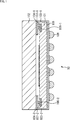
- FIG. 1 is a cross-sectional view showing a cross section of the semiconductor device 10 according to the first embodiment.
- the surface on which light is incident will be referred to as the upper surface (front surface) and the surface opposite to the front surface will be referred to as the lower surface (back surface).
- the left side surface is the left side surface
- the right side surface is the right side surface
- the front side surface is the front side surface
- the rear side surface is the side surface. It shall be called a rear side.
- a semiconductor device 10 is a semiconductor package in which a solid-state image sensor 101 is housed and packaged.
- the semiconductor device 10 includes a solid-state imaging device 101, a transparent member 102, a flexible printed circuit board 103-1 and a flexible printed circuit board 103-2, an adhesive 104-1 and an adhesive 104-2, an adhesive 105, a pad unit 106-1, and A pad section 106-2, bumps 107-1 and 107-2, and a plurality of external terminals (BGA: Ball Grid Array) 108 are formed.
- BGA Ball Grid Array
- the solid-state image sensor 101 is an image sensor such as a CMOS (Complementary Metal Oxide Semiconductor) image sensor or a CCD (Charge Coupled Device) image sensor.
- the solid-state imaging device 101 includes a pixel array unit in which a plurality of pixels having photoelectric conversion elements (for example, photodiodes) are two-dimensionally arranged in a matrix, and peripherals that perform pixel driving and A / D (Analog / Digital) conversion It consists of a circuit part.
- the flexible printed circuit board 103-1 uses a thin and flexible material as an insulator base material, and can be used in a deformed state. In FIG. 1, the flexible printed circuit board 103-1 is bent along each surface (upper surface, right side surface, and lower surface) of the solid-state imaging device 101.
- the flexible printed circuit board 103-1 includes (conductive) bumps 107-1 formed on the pad portion 106-1 provided on the upper surface (front surface) side of the solid-state image sensor 101, and the solid-state image sensor 101.
- Wiring (redistribution layer (RDL)) for connecting a plurality of external terminals (BGA) 108 provided on the lower surface (back surface) side is provided.
- the flexible printed circuit board 103-2 includes a (conductive) bump 107-2 formed on the pad portion 106-2 of the solid-state imaging device 101, and a plurality of external terminals (BGA). ) 108 is connected to each surface (redistribution (RDL)), and each surface (upper surface, left side surface, and lower surface) of the solid-state imaging device 101 so as to be symmetrical with the flexible printed circuit board 103-1. It is bent along.
- RDL redistribution
- the adhesive 104-1 and the adhesive 104-2 are provided on the surface along the upper surface (front surface) of the solid-state imaging device 101.
- the transparent member 102 is bonded (fixed).
- a cover glass or an IR filter can be used as the transparent member 102.
- a terminal (terminal 122-1 in FIG. 3A) provided on the surface of the flexible printed circuit 103-1 opposite to the surface to which the transparent member 102 is bonded is the pad portion 106- of the solid-state image sensor 101. 1 is electrically connected to the bump 107-1 formed on the substrate.
- the terminal (terminal 122-2 in FIG. 3A) provided on the surface of the flexible printed circuit 103-2 opposite to the surface to which the transparent member 102 is bonded is the pad portion 106 of the solid-state image sensor 101.
- -2 is electrically connected to the bump 107-2 formed on the -2.
- the solid-state image sensor 101 is bonded (fixed) to the surface along the lower surface (back surface) of the solid-state image sensor 101 by the adhesive 105.
- terminals terminals 123-1 and 123-2 in FIG. 3A
- BGA external terminals
- the semiconductor device 10 having the above-described structure, light from the subject passes through the transparent member 102 and is incident on the light receiving surface of the solid-state imaging device 101, and a signal corresponding to the incident light (the amount of light) is Via wiring formed on the flexible printed circuit boards 103-1 and 103-2 that are bent from the pad portions 106-1 and 106-2 of the solid-state imaging device 101 to the side surfaces (right side surface, left side surface) and lower surface (back surface).
- the data is output from a plurality of external terminals (BGA) 108.
- the end portions thereof do not cover the light receiving surface. (So as not to block incident light), that is, the position of the end is bent so as to be different from the position in the space on the light receiving surface. Accordingly, in the semiconductor device 10, the incident light is not blocked by the flexible printed circuit board 103-1 and the flexible printed circuit board 103-2, and an opening is formed with respect to the flexible printed circuit board 103-1 and the flexible printed circuit board 103-2. There is no need to provide.
- the flexible printed boards 103-1 and 103-2 need only be bent from the upper surface (front surface) of the solid-state imaging device 101 to the side surfaces (right side surface and left side surface) and the lower surface (back surface).
- a chip size package can be realized more simply by using the flexible printed circuit boards 103-1 and 103-2.
- the semiconductor device 10 of FIG. 1 uses the flexible printed boards 103-1 and 103-2, a chip size package can be realized without using a wafer technology such as a through silicon via (TSV). it can. Therefore, for example, there are no problems specific to the through silicon via (TSV) such as redistribution layer (RDL) peeling and corrosion of the pad (AI pad). Compared with this, the yield can be improved.
- TSV through silicon via
- an opening for exposing a light receiving surface of a solid-state imaging device is provided in a flexible printed circuit board.
- the number of sheets taken from the worksheet may be reduced when the flexible printed circuit board is manufactured as compared with a flexible printed circuit board without an opening.
- a solid-state image sensor having a large ratio of the light receiving surface (pixel region) to the chip area it is necessary to provide a wide opening, and the size of the flexible printed circuit board has to be increased accordingly. .
- the size of the semiconductor device semiconductor package
- the size of the solid-state imaging device chip for image sensor
- the solid-state imaging device 101 (for image sensor) has a larger number of pins (Pin) and a larger proportion of a light receiving surface (pixel region) with respect to the chip area Even if the chip is used, the widths of the flexible printed boards 103-1 and 103-2 do not become larger than the width of the solid-state image sensor 101, so all kinds of solid-state image sensors 101 (chips for image sensors) are used. ) Can be accommodated.
- the flexible printed boards 103-1 and 103-2 are simply bent from the upper surface (front surface) of the solid-state imaging device 101 to the side surfaces (right side surface and left side surface) and the lower surface (back surface).
- the plurality of external terminals (BGA) 108 are formed on the lower surface (back surface) side of the solid-state image sensor 101, the size of the semiconductor device 10 (semiconductor package) and the solid-state image sensor 101 (for image sensor) may be used. Chip size) is almost the same.
- the size of the semiconductor device 10 can be made substantially equal to the size of the solid-state imaging element 101, so that the semiconductor device 10 can be downsized.
- the rewiring (RDL) layout becomes easier as compared with the conventional chip-on-film, the cost for producing the flexible printed circuit boards 103-1 and 103-2 can be reduced.
- the flexible printed circuit board 103-1 and the flexible printed circuit board 103-2 are referred to as the flexible printed circuit board 103 when it is not necessary to distinguish them. Further, when it is not necessary to distinguish between the pad portion 106-1 and the pad portion 106-2, the pad portion 106-1 is referred to as a pad portion 106, and when it is not necessary to distinguish between the bump 107-1 and the bump 107-2, it is referred to as a bump 107.
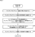
- the manufacturing process shown in FIG. 2 corresponds to a post-process, and the solid-state imaging device 101 is completed by the pre-process (wafer process).
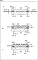
- 3 and 4 schematically show the manufacturing process of FIG. 2, and the detailed contents of each process in FIG. 2 will be described with reference to FIGS. 3 and 4 as appropriate. .
- step S11 a redistribution layer (RDL) formation process is performed.
- RDL 121-1 is formed on flexible printed circuit board 103-1, and the number depends on the number of pad portions 106-1 of solid-state image sensor 101. Terminals 122-1 and terminals 123-1 corresponding to the number of external terminals (BGA) 108 are formed. Note that slits 131-1 and 132-1 are formed on the flexible printed circuit board 103-1 for easy folding along each surface of the solid-state imaging device 101.
- an RDL 121-2 is formed on the flexible printed circuit board 103-2, and according to the number of terminals 122-2 and the number of external terminals (BGA) 108 according to the number of pads 106-2 of the solid-state image sensor 101.
- a terminal 123-2 is formed.
- slits 131-2 and 132-2 are also formed on the flexible printed circuit board 103-2.
- step S12 a substrate / transparent member bonding step is performed.
- the flexible printed circuit board 103-1 having the RDL 121-1 formed on the lower surface side of the transparent member 102 is bonded (fixed) with the adhesive 104-1.
- the flexible printed circuit board 103-2 on which the RDL 121-2 is formed is bonded (fixed) with the adhesive 104-2.
- a terminal 122-1 is provided on the surface opposite to the surface bonded to the transparent member 102 by the adhesive 104-1.
- a terminal 122-2 is provided on the surface of the flexible printed board 103-2 opposite to the surface bonded to the transparent member 102 by the adhesive 104-2.
- step S13 a flip chip bonding process is performed.
- bumps 107-1 are formed on the pad portion 106-1 provided on the light receiving surface side of the solid-state imaging device 101, and the pad portion 106-2 is formed. Then, the bump 107-2 is formed.
- the bump 107-1 formed on the pad portion 106-1 of the solid-state image sensor 101 and the terminal formed on the flexible printed circuit 103-1. 122-1 is connected, and the bump 107-2 formed on the pad portion 106-2 of the solid-state imaging device 101 and the terminal 122-2 formed on the flexible printed circuit board 103-2 are connected.
- seven terminals 122-1 are formed on the flexible printed circuit board 103-1, and seven terminals 122-2 (in FIG. 3) are formed on the flexible printed circuit board 103-2.
- A) is formed, but in the solid-state imaging device 101, pad portions 106 corresponding to those terminals 122 are provided, and bumps 107 are formed on each pad portion 106.
- the terminal 122 is connected.
- the flip chip bonding process is performed, and the solid-state imaging device 101 and the flexible printed circuit board 103-1 and the flexible printed circuit board 103-2 bonded to the transparent member 102 are electrically connected.
- step S14 a substrate / element bonding step is performed.
- the flexible printed circuit board 103-1 and the flexible printed circuit board 103-2 which are electrically connected to the solid-state imaging device 101 and bonded to the transparent member 102,
- the solid-state image sensor 101 is bent along each surface (side surface (right or left side) and lower surface) and bonded (fixed) to the lower surface (back surface) of the solid-state image sensor 101 with an adhesive 105.
- the flexible printed circuit board 103-1 bonded to the transparent member 102 is bent to the right side surface of the solid-state imaging device 101 by the slit 131-1, and further the slit 132. ⁇ 1 to be bent to the lower surface side of the solid-state imaging device 101.
- the flexible printed circuit board 103-2 bonded to the transparent member 102 is bent to the left side surface of the solid-state image sensor 101 by the slit 131-2, and further, the lower surface side of the solid-state image sensor 101 by the slit 132-2. Can be folded.
- step S15 an external terminal mounting step is performed.
- external terminals (BGA) 108 are mounted on the terminals 123-1 formed on the flexible printed circuit board 103-1, and the flexible printed circuit board 103-2.
- An external terminal (BGA) 108 is mounted on the formed terminal 123-2.
- the flexible printed circuit boards 103-1 and 103- having wirings for connecting the pad portion 106 provided on the upper surface side of the solid-state imaging device 101 and the external terminal (BGA) 108 provided on the lower surface side. 2 is bonded (fixed) to the transparent member 102, and the step of electrically connecting the pad portion 106 provided on the upper surface side of the solid-state imaging device 101 and the wiring of the flexible printed circuit boards 103-1 and 103-2. Done.
- the flexible printed circuit boards 103-1 and 103-2 are arranged in the solid-state image sensor 101 so that the position of the end portion on the upper surface side of the solid-state image sensor 101 is different from the position in the space on the light receiving surface. Bending along each surface, fixing the lower surface side of the solid-state image sensor 101 to the lower surface of the solid-state image sensor 101, and mounting external terminals (BGA) on the flexible printed boards 103-1 and 103-2
- the semiconductor device 10 of FIG. 1 is manufactured by performing the process to perform.
- the left and right side surfaces (left side surface and right side surface) of the solid-state image sensor 101 are covered by the flexible printed circuit board 103-1 and the flexible printed circuit board 103-2.
- a front side surface (front side surface) and a rear side surface (rear side surface) of 101 may be covered with the flexible printed circuit board 103-1 and the flexible printed circuit board 103-2.
- the solid-state image sensor 101 can be sealed. Thereby, in solid-state image sensor 101, it can prevent that dust adheres to the pixel array part in which a plurality of pixels are arranged two-dimensionally.
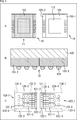
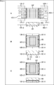
- FIG. 5 is a diagram illustrating the structure of the semiconductor device 10 according to the second embodiment.
- FIG. 5A is a top view of the semiconductor device 10.
- FIG. 5A the left side top view shows a state in which the transparent member 102 is attached in the semiconductor device 10, while the right side top view shows a state in which the transparent member 102 has been removed.
- the light receiving surface 111 of the solid-state image sensor 101 is exposed.
- the end portions of the flexible printed circuit board 103-1 and the flexible printed circuit board 103-2 do not cover the light receiving surface 111 (the incident light is not incident). In other words, it is bent so that the position of the end portion is different from the position in the space on the light receiving surface 111. Since the semiconductor device 10 has such a structure, incident light is not blocked by the flexible printed circuit board 103-1 and the flexible printed circuit board 103-2. There is no need to provide an opening for the substrate 103-2.
- FIG. 5B is a front view of the semiconductor device 10 and is a view when the semiconductor device 10 with the left transparent member 102 of FIG. 5A attached is viewed from the direction of the arrow F1. .
- the semiconductor device 10 according to the second embodiment not only the left side surface and the right side surface of the solid-state image sensor 101 but also the front side surface and the rear side surface of the solid-state image sensor 101 are flexible.
- the structure is covered with the printed circuit board 103-1 and the flexible printed circuit board 103-2.
- FIG. 5C shows the structures of the flexible printed circuit board 103-1 and the flexible printed circuit board 103-2 in the second embodiment.
- the flexible printed circuit board 103-1 is provided with a side surface bent portion 125-1 bent by the slit 133-1 and a side surface bent portion 126-1 bent by the slit 134-1.
- the flexible printed circuit board 103-2 is provided with a side surface bent portion 125-2 bent by the slit 133-2 and a side surface bent portion 126-2 bent by the slit 134-2.
- the flexible printed circuit board 103-1 and the flexible printed circuit board 103-2 having such a structure are formed on each surface (upper surface, side surface (right surface) of the solid-state imaging device 101, as in the first embodiment described above.
- the left side surface and the left side surface of the solid-state imaging device 101 can be covered by bending along the left side) and the lower surface.
- the side bent part 125-1 is bent by the slit 133-1
- the side bent part 125-2 is bent by the slit 133-2, so that solid-state imaging is performed.
- the front side surface of the element 101 can be covered.
- the side surface bent part 126-1 is bent by the slit 134-1
- the side surface bent part 126-2 is bent by the slit 134-2, so that solid-state imaging is performed.
- the rear side surface of the element 101 can be covered.
- the side surface bent portions of the flexible printed circuit board 103-1 and the flexible printed circuit board 103-2 not only the left and right side surfaces (left side surface and right side surface) of the solid-state imaging device 101 but also the front and back side surfaces.
- the front side surface and the rear side surface can also be covered with the flexible printed circuit board 103-1 and the flexible printed circuit board 103-2.
- the four side surfaces (left side surface, right side surface, front side surface, and rear side surface) of the solid-state image sensor 101 are covered with the flexible printed circuit board 103 and the solid-state image sensor 101 is sealed. Therefore, it is possible to prevent dust from adhering to each pixel arranged in the pixel array portion.
- FIG. 6 is a diagram illustrating each manufacturing process of the semiconductor device 10 according to the second embodiment.
- the manufacturing process of the semiconductor device 10 according to the second embodiment is performed basically in the same flow as the manufacturing process (FIG. 2) of the semiconductor device 10 according to the first embodiment described above.
- the substrate 103 is provided with side bent portions 125 and 126, and the side bent portions 125 and 126 cover the front and rear side surfaces (front side surface and rear side surface) of the solid-state imaging device 101.
- step S11 to S15 the respective steps in FIG. 2 and the schematic diagrams in FIG. 6 (A to C in FIG. 6) corresponding to these different points.
- the flow of the manufacturing process of the semiconductor device 10 according to the embodiment will be described.
- 6A to 6C show a top view and a front view of the semiconductor device 10, respectively.
- the rewiring (RDL) formation process (S11), the substrate, and the manufacturing process of the semiconductor device 10 of the first embodiment (FIG. 2)
- the transparent member bonding step (S12) is performed, and the flexible printed circuit board 103-1 having the RDL 121-1 formed on the lower surface side of the transparent member 102 is bonded (fixed) with the adhesive 104-1, and the RDL 121-2
- the flexible printed circuit board 103-2 on which is formed is bonded (fixed) by the adhesive 104-2.
- the flexible printed circuit board 103-1 is provided with a side surface bent part 125-1 and a side surface bent part 126-1
- the flexible printed circuit board 103-2 is provided with a side surface bent part 125-. 2 and side bent portions 126-2 are provided.
- bumps 107-1 are formed on the pad portion 106-1 provided on the light receiving surface side of the solid-state imaging device 101, and the bumps 107-1 are formed on the pad portion 106-2. -2 is formed.
- the flip chip bonding step (S13) as shown in FIG. 6A, the bump 107-1 formed on the pad portion 106-1 of the solid-state imaging device 101 and the flexible printed circuit board 103-1 are formed. Terminal 122-1 is connected, and bump 107-2 formed on pad portion 106-2 of solid-state image sensor 101 is connected to terminal 122-2 formed on flexible printed circuit board 103-2. Is done.
- the flip chip bonding step (S13) is performed, and the solid-state imaging device 101 is electrically connected to the flexible printed circuit board 103-1 and the flexible printed circuit board 103-2.
- the flexible printed circuit board 103-1 and the flexible printed circuit board that are electrically connected to the solid-state imaging device 101 and bonded to the transparent member 102. 103-2 is bent along each surface (upper surface, side surface (right side surface or left side surface), and lower surface) of the solid-state image sensor 101, and adhered to the lower surface (back surface) of the solid-state image sensor 101 by the adhesive 105. (Fixed).
- the flexible printed circuit board 103-1 and the flexible printed circuit board 103-2 are bent along each surface of the solid-state imaging device 101, and the left and right side surfaces (left side surface and right side surface) of the solid-state imaging device 101 are flexible printed circuit boards. 103.
- the side surface bent portion 125-1 and the side surface bent portion of the flexible printed circuit board 103-1 bonded to the lower surface (back surface) of the solid-state imaging device 101 are used.
- the portion 126-1 and the side surface bent portion 125-2 and the side surface bent portion 126-2 of the flexible printed circuit board 103-2 are bent to the respective side surfaces, and the front and rear side surfaces (front side surface and rear side surface) of the solid-state imaging device 101. Is covered with the flexible printed circuit board 103.
- the four side surfaces (left side surface, right side surface, front side surface, and rear side surface) of the solid-state imaging device 101 are covered with the flexible printed circuit board 103.
- the external terminals 123-1 formed on the flexible printed circuit board 103-1 are externally connected.
- Terminals (BGA) 108 are mounted, and external terminals (BGA) 108 are mounted on terminals 123-2 formed on flexible printed circuit board 103-2.
- the four sides of the solid-state image sensor 101 are surrounded by the flexible printed circuit board 103-1 and the flexible printed circuit board 103-2. Can be stopped. Thereby, in solid-state image sensor 101, it can prevent that dust adheres to the pixel array part in which a plurality of pixels are arranged two-dimensionally.
- the light receiving surface of the solid-state imaging device 101 is formed by the flexible printed circuit board 103-1 and the flexible printed circuit board 103-2 as in the semiconductor device 10 of the first embodiment. Therefore, it is not necessary to provide openings in the flexible printed circuit board 103-1 and the flexible printed circuit board 103-2.
- the solid-state image sensor 101 is configured such that the four side surfaces (left side surface, right side surface, front side surface, and rear side surface) of the solid-state image sensor 101 are surrounded by the flexible printed circuit board 103.
- each surface of the flexible printed circuit board 103 surrounding the four side surfaces of the solid-state imaging device 101 may have an arc shape having a predetermined curvature.
- a sealing member such as a resin Is used to seal the solid-state imaging device 101.
- the solid-state imaging device 101 it is possible to prevent dust from adhering to the pixel array portion in which a plurality of pixels are two-dimensionally arranged.
- the surface of the flexible printed circuit board 103 surrounding the four side surfaces (left side surface, right side surface, front side surface, and rear side surface) of the solid-state imaging device 101 has an arc shape, an external impact on the four side surfaces. Therefore, the solid-state image sensor 101 can be protected from external impacts.
- FIG. 7 is a diagram illustrating the structure of the semiconductor device 10 according to the third embodiment.
- FIG. 7A is a top view of the semiconductor device 10.
- FIG. 7B is a front view of the semiconductor device 10, and is a view when the semiconductor device 10 of FIG. 7A is viewed from the direction of the arrow F2.
- the side surface bent portion 125- 1 and a side bent portion 126-1 are provided, and the flexible printed circuit board 103-2 is provided with a side bent portion 125-2 and a side bent portion 126-2.
- the flexible printed circuit board 103-1 and the flexible printed circuit board 103-2 having such a structure are formed on each surface (upper surface, side surface (side surface)) of the solid-state imaging device 101 as in the second embodiment described above.
- the right side surface and the left side surface of the solid-state imaging device 101 can be covered by bending along the right side surface, the left side surface), and the lower surface.
- the surface of the flexible printed circuit board 103-1 covering the right side surface of the solid-state imaging device 101 has an arc shape having a predetermined curvature.
- the surface of the flexible printed circuit board 103-2 covering the left side surface of the solid-state image sensor 101 has an arc shape having a predetermined curvature.
- the side bent part 125-1 is bent by the slit 133-1
- the side bent part 125-2 is bent by the slit 133-2, so that solid-state imaging is performed.
- the front side surface of the element 101 can be covered.
- the surfaces of the flexible printed circuit board 103-1 and the flexible printed circuit board 103-2 that cover the front side surface of the solid-state imaging device 101 (the side surface bent portion 125-1 and the side surface bent portion 125-2).
- it has an arc shape having a predetermined curvature.
- the side surface bent part 126-1 is bent by the slit 134-1 and in the flexible printed circuit board 103-2, the side surface bent part 126-2 is bent by the slit 134-2, so that solid-state imaging is performed.
- the rear side surface of the element 101 can be covered.
- the surfaces of the flexible printed circuit board 103-1 and the flexible printed circuit board 103-2 that cover the rear surface of the solid-state imaging device 101 (the side surface bent portion 126-1 and the side surface bent portion 126-2).
- it has an arc shape having a predetermined curvature.
- the four side surfaces (left side surface, right side surface, front side surface, and rear side surface) of the solid-state imaging device 101 are surrounded by the flexible printed circuit board 103.
- the surface of the flexible printed circuit board 103 into an arc shape, in the semiconductor device 10, spaces are generated at the corners of the four corners.
- the solid-state imaging device 101 is sealed by sealing the spaces generated at the corners of the four corners using sealing members 151-1 to 151-4 such as resin.
- the four side surfaces (left side surface, right side surface, front side surface, and rear side surface) of the solid-state image sensor 101 are formed of the surface of the flexible printed circuit board 103 (arc shape having a predetermined curvature). Since the space formed at the corners of the four corners can be sealed by the sealing member 151, dust can be prevented from adhering to each pixel arranged in the pixel array portion. it can.
- the solid-state image sensor 101 can be protected from external impacts.
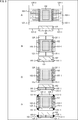
- FIG. 8 is a diagram for explaining each manufacturing process of the semiconductor device 10 according to the third embodiment.
- the manufacturing process of the semiconductor device 10 of the third embodiment is basically performed in the same flow as the manufacturing process (FIG. 2) of the semiconductor device 10 of the first embodiment described above.
- the substrate 103 is provided with side bent portions 125 and 126, and the side bent portions 125 and 126 surround the front and rear side surfaces of the solid-state image sensor 101 and the flexible printed circuit board 103 that surrounds the four side surfaces of the solid-state image sensor 101.
- Each of these surfaces differs in that it has an arc shape having a predetermined curvature and that the corners of the four corners are sealed by a sealing member 151.
- each step (steps S11 to S15) in FIG. 2 and the schematic diagram in FIG. 8 (A to D in FIG. 8) correspond to each other in the third implementation.
- the flow of the manufacturing process of the semiconductor device 10 according to the embodiment will be described. 8A to 8D, a top view and a front view of the semiconductor device 10 are shown, respectively.
- the rewiring (RDL) forming process (S11), the substrate, and the manufacturing process (FIG. 2) of the semiconductor device 10 of the first embodiment is performed, and the flexible printed circuit board 103-1 having the RDL 121-1 formed on the lower surface side of the transparent member 102 is bonded (fixed) with the adhesive 104-1, and the RDL 121-2
- the flexible printed circuit board 103-2 on which is formed is bonded (fixed) by the adhesive 104-2.
- the flexible printed circuit board 103-1 is provided with a side surface bent part 125-1 and a side surface bent part 126-1
- the flexible printed circuit board 103-2 is provided with a side surface bent part 125-. 2 and side bent portions 126-2 are provided.
- bumps 107-1 are formed on the pad portion 106-1 provided on the light receiving surface side of the solid-state imaging device 101, and the bumps 107-1 are formed on the pad portion 106-2. -2 is formed.
- the flip chip bonding step (S13) as shown in FIG. 8A, the bump 107-1 formed on the pad portion 106-1 of the solid-state imaging device 101 and the flexible printed circuit board 103-1 are formed. Terminal 122-1 is connected, and bump 107-2 formed on pad portion 106-2 of solid-state image sensor 101 is connected to terminal 122-2 formed on flexible printed circuit board 103-2. Is done.
- the flip chip bonding step (S13) is performed, and the solid-state imaging device 101 is electrically connected to the flexible printed circuit board 103-1 and the flexible printed circuit board 103-2.
- the flexible printed circuit board 103-1 and the flexible printed circuit board which are electrically connected to the solid-state imaging device 101 and bonded to the transparent member 102. 103-2 is bent along each surface (upper surface, side surface (right side surface or left side surface), and lower surface) of the solid-state image sensor 101, and adhered to the lower surface (back surface) of the solid-state image sensor 101 by the adhesive 105. (Fixed).
- the flexible printed circuit board 103-1 and the flexible printed circuit board 103-2 are bent along each surface of the solid-state imaging device 101, and the left and right side surfaces (right side surface and left side surface) of the solid-state imaging device 101 are flexible printed circuit boards.
- Each surface of the flexible printed circuit board 103 on the left and right side surfaces has an arc shape having a predetermined curvature.
- the arrow height (arc height) can be set to be equal to or less than the thickness of the solid-state imaging device 101, for example.
- the side surface bent portion 125-1 and the side surface bent portion of the flexible printed circuit board 103-1 bonded to the lower surface (back surface) of the solid-state imaging device 101 are used.
- the portion 126-1 and the side surface bent portion 125-2 and the side surface bent portion 126-2 of the flexible printed circuit board 103-2 are bent to the respective side surfaces, and the front and rear side surfaces (front side surface and rear side surface) of the solid-state imaging device 101. Is surrounded by the flexible printed circuit board 103.
- each surface (side surface bent portions 125-1 and 125-2 and side surface bent portions 126-1 and 126-2) of the flexible printed circuit board 103 on the side surface before and after the solid-state imaging device 101 has a predetermined curvature. It has an arc shape.
- the height of the arc can be set to be equal to or less than the thickness of the solid-state image sensor 101, for example.
- the four side surfaces (left side surface, right side surface, front side surface, and rear side surface) of the solid-state imaging device 101 are surrounded by the flexible printed circuit board 103.
- the surface of the flexible printed circuit board 103 into an arc shape, in the semiconductor device 10, spaces are generated at the corners of the four corners. Therefore, in the substrate / element bonding step (S14), as shown in FIG. 8D, the spaces formed at the corners of the four corners are sealed using sealing members 151-1 to 151-4 such as resin. To do.
- the external terminals 123-1 formed on the flexible printed circuit board 103-1 are externally connected.
- Terminals (BGA) 108 are mounted, and external terminals (BGA) 108 are mounted on terminals 123-2 formed on flexible printed circuit board 103-2.
- the surface of the flexible printed circuit board 103 surrounding the four side surfaces (the left side surface, the right side surface, the front side surface, and the rear side surface) of the solid-state imaging device 101 is predetermined. Therefore, the solid-state imaging device 101 can be protected from external impacts because it is strong against external impacts on the four side surfaces.
- each surface of the flexible printed circuit board 103 in an arc shape, spaces are generated at the corners of the four corners of the semiconductor device 10, but sealing members 151-1 to 151-4 such as resin are used.
- sealing members 151-1 to 151-4 such as resin are used.
- the case where two flexible printed boards 103 (flexible printed boards 103-1 and 103-2) are used has been described as an example.
- the present technology is not limited by the number of flexible printed circuit boards 103, and one or three or more flexible printed circuit boards 103 may be used as long as the above-described functions can be realized.
- the spaces generated at the four corners of the semiconductor device 10 are sealed by the sealing members 151-1 to 151-4. There is no.
- the solid-state image sensor 101 cannot be sealed, but the surface of the flexible printed circuit board 103 surrounding the four side surfaces of the solid-state image sensor 101 has an arc shape. You can protect from. Further, it is not necessary that all surfaces of the flexible printed circuit board 103 surrounding the four side surfaces of the solid-state imaging device 101 have an arc shape, and only a part of the surfaces may have an arc shape.
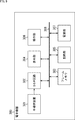
- FIG. 9 is a diagram illustrating a configuration example of an electronic apparatus 300 having a semiconductor device to which the present technology is applied.
- an electronic device such as an imaging device such as a digital still camera or a video camera, or a mobile terminal device such as a smartphone or a tablet terminal.
- the electronic device 300 includes a semiconductor device 301, a DSP circuit 302, a frame memory 303, a display unit 304, a recording unit 305, an operation unit 306, and a power supply unit 307.
- the DSP circuit 302, the frame memory 303, the display unit 304, the recording unit 305, the operation unit 306, and the power supply unit 307 are connected to each other via a bus line 308.
- the semiconductor device 301 corresponds to the semiconductor device 10 of the first to third embodiments, and has, for example, the cross-sectional structure of FIG.
- the DSP circuit 302 is a camera signal processing circuit that processes a signal supplied from the semiconductor device 301 (the solid-state imaging device 101).
- the DSP circuit 302 outputs image data obtained by processing a signal from the semiconductor device 301.
- the frame memory 303 temporarily holds the image data processed by the DSP circuit 302 in units of frames.
- the display unit 304 includes a panel type display device such as a liquid crystal panel or an organic EL (Electro Luminescence) panel, for example, and displays a moving image or a still image captured by the semiconductor device 301 (the solid-state image sensor 101).
- the recording unit 305 records image data of a moving image or a still image captured by the semiconductor device 301 (the solid-state imaging device 101) on a recording medium such as a semiconductor memory or a hard disk.
- the operation unit 306 outputs operation commands for various functions of the electronic device 300 in accordance with user operations.
- the power supply unit 307 appropriately supplies various power sources serving as operation power sources for the DSP circuit 302, the frame memory 303, the display unit 304, the recording unit 305, and the operation unit 306 to these supply targets.
- the electronic device 300 is configured as described above.
- FIG. 10 is a diagram illustrating a usage example of the semiconductor device 10 including the solid-state imaging device 101 as an image sensor.
- the semiconductor device 10 described above can be used in various cases for sensing light such as visible light, infrared light, ultraviolet light, and X-rays as follows. That is, as shown in FIG. 10, not only the above-mentioned field of appreciation for taking images to be used for appreciation, but also, for example, the field of transportation, the field of home appliances, the field of medical / healthcare, the field of security.
- the semiconductor device 10 can also be used in a device used in the field of beauty, the field of sports, the field of agriculture, or the like.
- a device for shooting an image used for viewing such as a digital camera, a smartphone, or a mobile phone with a camera function (for example, FIG. 9).
- the semiconductor device 10 can be used in the electronic apparatus 300).
- the semiconductor device 10 can be used as a device used for traffic such as a monitoring camera and a distance measuring sensor for measuring a distance between vehicles.
- the semiconductor device 10 is a device used for home appliances such as a television receiver, a refrigerator, and an air conditioner. Can be used. Further, in the medical / healthcare field, for example, the semiconductor device 10 is used in a device used for medical or health care such as an endoscope or a device that performs angiography by receiving infrared light. be able to.
- the semiconductor device 10 can be used in an apparatus provided for security, such as a security camera or a person authentication camera.
- the semiconductor device 10 can be used in a device used for beauty, such as a skin measuring device for photographing the skin and a microscope for photographing the scalp.
- the semiconductor device 10 can be used in devices used for sports such as action cameras and wearable cameras for sports applications.
- the semiconductor device 10 can be used in an apparatus used for agriculture, such as a camera for monitoring the state of fields and crops.
- the present technology can take the following configurations.
- a solid-state imaging device having a pixel array unit in which a plurality of pixels each having a photoelectric conversion element are arranged in a two-dimensional matrix;
- a flexible printed circuit board having wiring for connecting a pad portion provided on the upper surface side which is the light receiving surface side of the solid-state imaging device and an external terminal provided on the lower surface side opposite to the upper surface side;
- the flexible printed circuit board is disposed along each surface of the solid-state imaging device such that the position of the end portion on the upper surface side is different from the position in the space on the light receiving surface.
- the flexible printed circuit board includes a first flexible printed circuit board and a second flexible printed circuit board,
- the first flexible printed circuit board is bent along an upper surface, one side surface of four side surfaces, and a lower surface of the solid-state imaging device,
- the first flexible printed circuit board is fixed to the solid-state imaging device in a partial region of one surface, and fixed to the transparent member in a partial region of the other surface
- the second flexible printed circuit board is fixed to the solid-state imaging device in a partial region on one surface, and fixed to the transparent member in a partial region on the other surface.
- the first flexible printed circuit board is In order to seal the solid-state image sensor, the solid-state image sensor has a first side surface bent portion that is bent along the remaining two side surfaces among the four side surfaces of the solid-state image sensor,
- the second flexible printed circuit board is The semiconductor device according to (3), further including a second side-surface bent portion that is bent along the remaining two side surfaces among the four side surfaces of the solid-state image sensor to seal the solid-state image sensor.
- the surface bent along the four side surfaces of the solid-state imaging device has an arc shape having a predetermined curvature. apparatus.
- the semiconductor according to (5) further comprising: a sealing member for sealing a space generated by forming a surface bent along four side surfaces of the solid-state imaging device into an arc shape having a predetermined curvature. apparatus.
- a sealing member for sealing a space generated by forming a surface bent along four side surfaces of the solid-state imaging device into an arc shape having a predetermined curvature. apparatus.
- the sealing member is a resin.
- the first flexible printed circuit board and the second flexible printed circuit board are formed with a slit in a bent portion.
- a flexible printed circuit board having wiring for connecting a pad portion provided on the upper surface side, which is the light receiving surface side of the solid-state imaging device, and an external terminal provided on the lower surface side opposite to the upper surface side is incident on the light receiving surface.
- a solid-state imaging device having a pixel array unit in which a plurality of pixels each having a photoelectric conversion element are arranged in a two-dimensional matrix;
- a flexible printed circuit board having wiring for connecting a pad portion provided on the upper surface side, which is the light receiving surface side of the solid-state imaging device, and an external terminal provided on the lower surface side opposite to the upper surface side;
- the flexible printed circuit board is disposed along each surface of the solid-state imaging device so that the position of the end portion on the upper surface side is different from the position in the space on the light receiving surface. Equipped with electronic equipment.
- 10 semiconductor device 101 solid-state imaging device, 102 transparent member, 103, 103-1, 103-2 flexible printed circuit board, 104-1, 104-2 adhesive, 105 adhesive, 106-1, 106-2 pad part, 107-1, 107-2 bumps, 108 external terminals, 125-1, 125-2, 126-1, 126-2 side bent parts, 151-1, 151-2, 151-3, 151-4 sealing members , 300 electronic devices, 301 semiconductor devices
Landscapes
- Engineering & Computer Science (AREA)
- Multimedia (AREA)
- Signal Processing (AREA)
- Solid State Image Pick-Up Elements (AREA)
- Physics & Mathematics (AREA)
- Electromagnetism (AREA)
- Transforming Light Signals Into Electric Signals (AREA)
Abstract
La présente invention porte sur un dispositif à semi-conducteur grâce auquel un boîtier de la taille d'une puce peut être plus simple à réaliser en utilisant une carte de circuit imprimé souple. L'invention porte également sur son procédé de fabrication, et un dispositif électronique. Le dispositif à semi-conducteur de l'invention comporte : un élément de capture d'image à semi-conducteur comprenant une partie matrice de pixels dans laquelle une pluralité de pixels comprenant des éléments de conversion photoélectrique sont disposés en une matrice bidimensionnelle; et une carte de circuit imprimé souple comprenant un câblage servant à connecter une partie plage de connexion, disposée du côté d'une surface supérieure de l'élément de capture d'image à semi-conducteur, qui est son côté surface de réception de lumière, à une borne externe disposée du côté d'une surface inférieure située du côté opposé au côté surface supérieure, la carte de circuit imprimé souple étant disposée le long de chaque surface de l'élément de capture d'image à semi-conducteur de manière qu'une partie d'extrémité de la carte de circuit imprimé souple côté surface supérieure de la carte de circuit imprimé souple soit disposée dans une position différente d'une position dans un espace au-dessus de la surface de réception de lumière. La présente invention peut être appliquée lors de la mise sous boîtier d'un capteur d'image CMOS, par exemple.
Priority Applications (1)
| Application Number | Priority Date | Filing Date | Title |
|---|---|---|---|
| US15/743,911 US11171170B2 (en) | 2015-07-28 | 2016-07-14 | Image sensor package with flexible printed circuits |
Applications Claiming Priority (2)
| Application Number | Priority Date | Filing Date | Title |
|---|---|---|---|
| JP2015148682A JP2017028226A (ja) | 2015-07-28 | 2015-07-28 | 半導体装置及びその製造方法、並びに電子機器 |
| JP2015-148682 | 2015-07-28 |
Publications (1)
| Publication Number | Publication Date |
|---|---|
| WO2017018231A1 true WO2017018231A1 (fr) | 2017-02-02 |
Family
ID=57886910
Family Applications (1)
| Application Number | Title | Priority Date | Filing Date |
|---|---|---|---|
| PCT/JP2016/070874 Ceased WO2017018231A1 (fr) | 2015-07-28 | 2016-07-14 | Dispositif à semi-conducteur, son procédé de fabrication, et dispositif électronique |
Country Status (3)
| Country | Link |
|---|---|
| US (1) | US11171170B2 (fr) |
| JP (1) | JP2017028226A (fr) |
| WO (1) | WO2017018231A1 (fr) |
Cited By (1)
| Publication number | Priority date | Publication date | Assignee | Title |
|---|---|---|---|---|
| WO2024009694A1 (fr) * | 2022-07-05 | 2024-01-11 | ソニーセミコンダクタソリューションズ株式会社 | Dispositif à semi-conducteur, appareil électronique et procédé de production de dispositif à semi-conducteur |
Families Citing this family (6)
| Publication number | Priority date | Publication date | Assignee | Title |
|---|---|---|---|---|
| CN108606775A (zh) * | 2018-03-23 | 2018-10-02 | 天津大学 | 分布式柔性生物电子器件及多层柔性通道的制备方法 |
| US11201096B2 (en) * | 2019-07-09 | 2021-12-14 | Texas Instruments Incorporated | Packaged device with die wrapped by a substrate |
| JP2022187526A (ja) * | 2021-06-08 | 2022-12-20 | ソニーセミコンダクタソリューションズ株式会社 | 撮像素子パッケージおよび電子機器 |
| US12148741B2 (en) | 2021-08-20 | 2024-11-19 | Apple Inc. | Sidewall connections and button interconnects for molded SiPs |
| US11765838B2 (en) | 2021-08-20 | 2023-09-19 | Apple Inc. | Right angle sidewall and button interconnects for molded SiPs |
| JP7761435B2 (ja) * | 2021-09-29 | 2025-10-28 | アオイ電子株式会社 | 半導体装置の製造方法および半導体装置 |
Citations (4)
| Publication number | Priority date | Publication date | Assignee | Title |
|---|---|---|---|---|
| WO2004055891A1 (fr) * | 2002-12-17 | 2004-07-01 | Fujitsu Limited | Dispositif a semi-conducteurs et dispositif a empilement de semi-conducteurs |
| US20060087018A1 (en) * | 2004-10-21 | 2006-04-27 | Chipmos Technologies (Bermuda) Ltd. | Multi-chip image sensor module |
| US20060261458A1 (en) * | 2003-11-12 | 2006-11-23 | Amkor Technology, Inc. | Semiconductor package and manufacturing method thereof |
| JP2012517716A (ja) * | 2009-02-11 | 2012-08-02 | メギカ・コーポレイション | イメージおよび光センサチップパッケージ |
Family Cites Families (8)
| Publication number | Priority date | Publication date | Assignee | Title |
|---|---|---|---|---|
| JP3377757B2 (ja) * | 1999-01-04 | 2003-02-17 | シャープ株式会社 | 液晶パネル駆動用集積回路パッケージおよび液晶パネルモジュール |
| CN1185915C (zh) * | 2001-06-13 | 2005-01-19 | 佳能株式会社 | 柔性基板、半导体器件、摄像装置和放射线摄像系统 |
| US20050104186A1 (en) * | 2003-11-14 | 2005-05-19 | International Semiconductor Technology Ltd. | Chip-on-film package for image sensor and method for manufacturing the same |
| JP2006324304A (ja) | 2005-05-17 | 2006-11-30 | Yuutekku System:Kk | 半導体パッケージ及びイメージセンサー型モジュール |
| TWI344680B (en) * | 2007-04-02 | 2011-07-01 | Siliconware Precision Industries Co Ltd | Sensor-type semiconductor device and manufacturing method thereof |
| US9402303B2 (en) * | 2013-06-03 | 2016-07-26 | Apple Inc. | Flexible printed circuit cables with slits |
| JP5727076B2 (ja) * | 2013-06-27 | 2015-06-03 | キヤノン・コンポーネンツ株式会社 | フレキシブルプリント配線板、フレキシブル回路板およびそれを用いた電子装置 |
| US9583445B2 (en) * | 2014-03-18 | 2017-02-28 | Apple Inc. | Metal electromagnetic interference (EMI) shielding coating along an edge of a ceramic substrate |
-
2015
- 2015-07-28 JP JP2015148682A patent/JP2017028226A/ja active Pending
-
2016
- 2016-07-14 WO PCT/JP2016/070874 patent/WO2017018231A1/fr not_active Ceased
- 2016-07-14 US US15/743,911 patent/US11171170B2/en not_active Expired - Fee Related
Patent Citations (4)
| Publication number | Priority date | Publication date | Assignee | Title |
|---|---|---|---|---|
| WO2004055891A1 (fr) * | 2002-12-17 | 2004-07-01 | Fujitsu Limited | Dispositif a semi-conducteurs et dispositif a empilement de semi-conducteurs |
| US20060261458A1 (en) * | 2003-11-12 | 2006-11-23 | Amkor Technology, Inc. | Semiconductor package and manufacturing method thereof |
| US20060087018A1 (en) * | 2004-10-21 | 2006-04-27 | Chipmos Technologies (Bermuda) Ltd. | Multi-chip image sensor module |
| JP2012517716A (ja) * | 2009-02-11 | 2012-08-02 | メギカ・コーポレイション | イメージおよび光センサチップパッケージ |
Cited By (1)
| Publication number | Priority date | Publication date | Assignee | Title |
|---|---|---|---|---|
| WO2024009694A1 (fr) * | 2022-07-05 | 2024-01-11 | ソニーセミコンダクタソリューションズ株式会社 | Dispositif à semi-conducteur, appareil électronique et procédé de production de dispositif à semi-conducteur |
Also Published As
| Publication number | Publication date |
|---|---|
| US20180204870A1 (en) | 2018-07-19 |
| JP2017028226A (ja) | 2017-02-02 |
| US11171170B2 (en) | 2021-11-09 |
Similar Documents
| Publication | Publication Date | Title |
|---|---|---|
| WO2017018231A1 (fr) | Dispositif à semi-conducteur, son procédé de fabrication, et dispositif électronique | |
| US11862656B2 (en) | Semiconductor device and manufacturing method, and electronic appliance | |
| JP6822399B2 (ja) | 固体撮像装置およびその製造方法、並びに電子機器 | |
| US11043436B2 (en) | Semiconductor device, manufacturing method, imaging device, and electronic apparatus for enabling component mounting with high flatness | |
| KR20180097522A (ko) | 고체 촬상 소자 및 전자 장치 | |
| JP6743035B2 (ja) | 撮像装置、製造方法 | |
| CN108886024B (zh) | 半导体装置、半导体装置制造方法、集成基板和电子设备 | |
| CN108701696B (zh) | 玻璃中介层模块、成像装置和电子设备 | |
| US9515108B2 (en) | Image sensors with contamination barrier structures | |
| TWI746620B (zh) | 相機模組、製造方法及電子機器 | |
| KR20190116276A (ko) | 고체 촬상 장치 및 전자 기기 | |
| JP6990317B2 (ja) | 撮像ユニット及び撮像装置 | |
| JP7721567B2 (ja) | 固体撮像素子、製造方法、および電子機器 | |
| US12356753B2 (en) | Imaging device and method for manufacturing imaging device | |
| WO2025105035A1 (fr) | Boîtier de semi-conducteur, dispositif à semi-conducteur et procédé de fabrication de boîtier de semi-conducteur | |
| JP2026513688A (ja) | イメージセンサーモジュール、カメラモジュール及びその製造方法 | |
| JP2016076616A (ja) | 半導体装置、製造装置、製造方法 | |
| WO2022113813A1 (fr) | Boîtier d'élément d'imagerie, procédé de fabrication et appareil électronique |
Legal Events
| Date | Code | Title | Description |
|---|---|---|---|
| 121 | Ep: the epo has been informed by wipo that ep was designated in this application |
Ref document number: 16830336 Country of ref document: EP Kind code of ref document: A1 |
|
| WWE | Wipo information: entry into national phase |
Ref document number: 15743911 Country of ref document: US |
|
| NENP | Non-entry into the national phase |
Ref country code: DE |
|
| 122 | Ep: pct application non-entry in european phase |
Ref document number: 16830336 Country of ref document: EP Kind code of ref document: A1 |