WO2017018242A1 - Module haut-parleur, et dispositif électronique - Google Patents
Module haut-parleur, et dispositif électronique Download PDFInfo
- Publication number
- WO2017018242A1 WO2017018242A1 PCT/JP2016/070944 JP2016070944W WO2017018242A1 WO 2017018242 A1 WO2017018242 A1 WO 2017018242A1 JP 2016070944 W JP2016070944 W JP 2016070944W WO 2017018242 A1 WO2017018242 A1 WO 2017018242A1
- Authority
- WO
- WIPO (PCT)
- Prior art keywords
- speaker
- magnetic substrate
- speaker module
- switching circuit
- circuit element
- Prior art date
- Legal status (The legal status is an assumption and is not a legal conclusion. Google has not performed a legal analysis and makes no representation as to the accuracy of the status listed.)
- Ceased
Links
Images





Classifications
-
- G—PHYSICS
- G06—COMPUTING OR CALCULATING; COUNTING
- G06F—ELECTRIC DIGITAL DATA PROCESSING
- G06F1/00—Details not covered by groups G06F3/00 - G06F13/00 and G06F21/00
- G06F1/16—Constructional details or arrangements
- G06F1/1613—Constructional details or arrangements for portable computers
- G06F1/1633—Constructional details or arrangements of portable computers not specific to the type of enclosures covered by groups G06F1/1615 - G06F1/1626
- G06F1/1684—Constructional details or arrangements related to integrated I/O peripherals not covered by groups G06F1/1635 - G06F1/1675
- G06F1/1688—Constructional details or arrangements related to integrated I/O peripherals not covered by groups G06F1/1635 - G06F1/1675 the I/O peripheral being integrated loudspeakers
-
- G—PHYSICS
- G06—COMPUTING OR CALCULATING; COUNTING
- G06F—ELECTRIC DIGITAL DATA PROCESSING
- G06F1/00—Details not covered by groups G06F3/00 - G06F13/00 and G06F21/00
- G06F1/16—Constructional details or arrangements
- G06F1/1613—Constructional details or arrangements for portable computers
- G06F1/1626—Constructional details or arrangements for portable computers with a single-body enclosure integrating a flat display, e.g. Personal Digital Assistants [PDAs]
-
- H—ELECTRICITY
- H04—ELECTRIC COMMUNICATION TECHNIQUE
- H04M—TELEPHONIC COMMUNICATION
- H04M1/00—Substation equipment, e.g. for use by subscribers
- H04M1/02—Constructional features of telephone sets
-
- H—ELECTRICITY
- H04—ELECTRIC COMMUNICATION TECHNIQUE
- H04M—TELEPHONIC COMMUNICATION
- H04M1/00—Substation equipment, e.g. for use by subscribers
- H04M1/60—Substation equipment, e.g. for use by subscribers including speech amplifiers
- H04M1/6016—Substation equipment, e.g. for use by subscribers including speech amplifiers in the receiver circuit
-
- H—ELECTRICITY
- H04—ELECTRIC COMMUNICATION TECHNIQUE
- H04R—LOUDSPEAKERS, MICROPHONES, GRAMOPHONE PICK-UPS OR LIKE ACOUSTIC ELECTROMECHANICAL TRANSDUCERS; ELECTRIC HEARING AIDS; PUBLIC ADDRESS SYSTEMS
- H04R1/00—Details of transducers, loudspeakers or microphones
-
- H—ELECTRICITY
- H04—ELECTRIC COMMUNICATION TECHNIQUE
- H04R—LOUDSPEAKERS, MICROPHONES, GRAMOPHONE PICK-UPS OR LIKE ACOUSTIC ELECTROMECHANICAL TRANSDUCERS; ELECTRIC HEARING AIDS; PUBLIC ADDRESS SYSTEMS
- H04R1/00—Details of transducers, loudspeakers or microphones
- H04R1/02—Casings; Cabinets ; Supports therefor; Mountings therein
-
- H—ELECTRICITY
- H04—ELECTRIC COMMUNICATION TECHNIQUE
- H04R—LOUDSPEAKERS, MICROPHONES, GRAMOPHONE PICK-UPS OR LIKE ACOUSTIC ELECTROMECHANICAL TRANSDUCERS; ELECTRIC HEARING AIDS; PUBLIC ADDRESS SYSTEMS
- H04R9/00—Transducers of moving-coil, moving-strip, or moving-wire type
- H04R9/06—Loudspeakers
-
- H—ELECTRICITY
- H04—ELECTRIC COMMUNICATION TECHNIQUE
- H04R—LOUDSPEAKERS, MICROPHONES, GRAMOPHONE PICK-UPS OR LIKE ACOUSTIC ELECTROMECHANICAL TRANSDUCERS; ELECTRIC HEARING AIDS; PUBLIC ADDRESS SYSTEMS
- H04R1/00—Details of transducers, loudspeakers or microphones
- H04R1/02—Casings; Cabinets ; Supports therefor; Mountings therein
- H04R1/025—Arrangements for fixing loudspeaker transducers, e.g. in a box, furniture
-
- H—ELECTRICITY
- H04—ELECTRIC COMMUNICATION TECHNIQUE
- H04R—LOUDSPEAKERS, MICROPHONES, GRAMOPHONE PICK-UPS OR LIKE ACOUSTIC ELECTROMECHANICAL TRANSDUCERS; ELECTRIC HEARING AIDS; PUBLIC ADDRESS SYSTEMS
- H04R2201/00—Details of transducers, loudspeakers or microphones covered by H04R1/00 but not provided for in any of its subgroups
- H04R2201/02—Details casings, cabinets or mounting therein for transducers covered by H04R1/02 but not provided for in any of its subgroups
- H04R2201/028—Structural combinations of loudspeakers with built-in power amplifiers, e.g. in the same acoustic enclosure
-
- H—ELECTRICITY
- H04—ELECTRIC COMMUNICATION TECHNIQUE
- H04R—LOUDSPEAKERS, MICROPHONES, GRAMOPHONE PICK-UPS OR LIKE ACOUSTIC ELECTROMECHANICAL TRANSDUCERS; ELECTRIC HEARING AIDS; PUBLIC ADDRESS SYSTEMS
- H04R2499/00—Aspects covered by H04R or H04S not otherwise provided for in their subgroups
- H04R2499/10—General applications
- H04R2499/11—Transducers incorporated or for use in hand-held devices, e.g. mobile phones, PDA's, camera's
-
- H—ELECTRICITY
- H04—ELECTRIC COMMUNICATION TECHNIQUE
- H04R—LOUDSPEAKERS, MICROPHONES, GRAMOPHONE PICK-UPS OR LIKE ACOUSTIC ELECTROMECHANICAL TRANSDUCERS; ELECTRIC HEARING AIDS; PUBLIC ADDRESS SYSTEMS
- H04R3/00—Circuits for transducers
-
- H—ELECTRICITY
- H04—ELECTRIC COMMUNICATION TECHNIQUE
- H04R—LOUDSPEAKERS, MICROPHONES, GRAMOPHONE PICK-UPS OR LIKE ACOUSTIC ELECTROMECHANICAL TRANSDUCERS; ELECTRIC HEARING AIDS; PUBLIC ADDRESS SYSTEMS
- H04R9/00—Transducers of moving-coil, moving-strip, or moving-wire type
- H04R9/02—Details
- H04R9/025—Magnetic circuit
Definitions
- the present invention relates to a speaker module, and more particularly to a speaker module mounted on an electronic device that requires high-density mounting.
- a speaker element and a speaker-related component such as an amplifier circuit element for a speaker element or a DCDC converter element are integrated as a speaker module from the viewpoint of high-density mounting. It is conceivable to configure.
- the speaker may be affected by noise radiated from the DCDC converter element.
- the arrangement of the speaker module and the DCDC converter element is restricted, which becomes a factor that hinders high-density mounting.
- an object of the present invention is to provide a speaker module and an electronic device that can be mounted at high density.
- a speaker module includes a switching circuit element, a DCDC converter element having a choke coil connected to the switching circuit element, and an output voltage of the DCDC converter element. And a speaker element for converting the electric signal generated by the sound into sound, the choke coil is built in between the switching circuit element and the speaker element, and the magnetic circuit board on which the switching circuit element is mounted Is arranged.
- radiation magnetic noise can be suppressed by arranging the magnetic substrate with the built-in choke coil between the switching circuit element and the speaker element.
- the magnetic substrate serves as an electromagnetic shield, radiation noise from the choke coil, the switching circuit element, and the wiring (conductor) connecting them can be suppressed. Therefore, since the speaker element and the DCDC converter element are arranged close to each other and a reduction in the degree of freedom of arrangement of the speaker module can be suppressed, high-density mounting can be achieved.
- the speaker module further includes an amplifier circuit element that generates the electrical signal by amplifying using the output voltage of the DCDC converter element, and the amplifier circuit element includes the switching circuit of the magnetic substrate. It may be mounted on the mounting surface of the element.
- the amplification circuit element is mounted on the mounting surface of the switching circuit element on the magnetic substrate, it is possible to increase the output (increase the volume) while suppressing radiation noise.
- the magnetic substrate is disposed between the amplifier circuit element and the speaker element, it is possible to suppress a decrease in the degree of freedom in arranging the speaker module while arranging the speaker element and the amplifier circuit element in close proximity. Therefore, it is possible to increase the output while achieving high-density mounting of the speaker module.
- the magnetic substrate may have vias penetrating at least part of the magnetic substrate, and the speaker element may convert the electric signal input through the vias.
- the speaker element converts an electric signal input through a via penetrating at least a part of the magnetic substrate into sound. For this reason, since the magnetic substrate through which the via penetrates functions as a ferrite bead, noise of the electric signal can be suppressed, so that sound quality can be improved.
- the speaker element may be mounted on one main surface of the magnetic substrate, and the switching circuit element may be mounted on the other main surface of the magnetic substrate.
- the speaker element is mounted on one main surface of the magnetic substrate and the switching circuit element is mounted on the other main surface, the shape in plan view can be reduced. That is, according to this aspect, a speaker module excellent in space saving can be realized.
- a flexible substrate in which the speaker element is mounted on one main surface and the magnetic substrate is mounted on the other main surface may be provided.
- a speaker element is mounted on one main surface and a flexible substrate with a magnetic substrate mounted on the other main surface is provided, so that the speaker module and other components are connected by the flexible substrate. It becomes possible to do. For this reason, since it becomes possible to connect a speaker module and the said other components, without providing connection parts, such as a connector which may become a factor which hinders size reduction of a speaker module, further high-density mounting is achieved. .
- the flexible substrate includes a first portion on which the speaker element is mounted and a second portion on which the magnetic substrate is mounted, and the second portion is in relation to the first portion. You may decide to arrange
- the second portion is arranged on the side of the speaker element in a state bent with respect to the first portion, the magnetic substrate is arranged on the side of the speaker element. For this reason, the speaker module can be reduced in height.
- a printed wiring board in which the speaker element is mounted on one main surface and the magnetic substrate is mounted on the other main surface may be provided.
- the speaker module is manufactured by a general versatile manufacturing process. Can do.
- the speaker element has a voice coil that vibrates when the electric signal flows, and the choke coil and the voice coil are arranged so that winding axes are in an arbitrary positional relationship different from parallel. You may decide.
- an electronic device is an electronic device including a speaker module, and the speaker module includes a switching circuit element and a DCDC converter element having a choke coil connected to the switching circuit element.
- the speaker module includes a switching circuit element and a DCDC converter element having a choke coil connected to the switching circuit element.
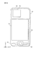
- FIG. 1A is a top view illustrating an example of an appearance of the mobile terminal device according to the embodiment.
- FIG. 1B is a top view showing an internal configuration of the mobile terminal device according to the embodiment.
- FIG. 2 is a block diagram illustrating an example of a functional configuration of the mobile terminal device according to the embodiment.
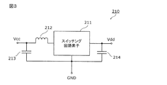
- FIG. 3 is a circuit diagram showing an example of a circuit of the DCDC converter element according to the embodiment.
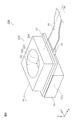
- FIG. 4 is a perspective view showing an example of the configuration of the speaker module according to the embodiment.
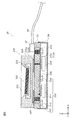
- FIG. 5 is a cross-sectional view showing an example of the configuration of the speaker module according to the embodiment.
- FIG. 6 is a perspective view illustrating an example of a configuration of a speaker module according to Modification 1 of the embodiment.
- FIG. 1A is a top view illustrating an example of an appearance of the mobile terminal device according to the embodiment.
- FIG. 1B is a top view showing an internal configuration of the mobile terminal device according to the embodiment.
- FIG. 2 is a
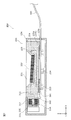
- FIG. 7 is a cross-sectional view illustrating an example of a configuration of a speaker module according to Modification 1 of the embodiment.
- FIG. 8 is a perspective view illustrating an example of a configuration of a speaker module according to Modification 2 of the embodiment.
- FIG. 9 is a cross-sectional view illustrating an example of a configuration of a speaker module according to Modification 2 of the embodiment.
- FIG. 1A is a top view illustrating an example of an appearance of the mobile terminal device 1 according to the embodiment.
- FIG. 1B is a top view showing the internal configuration of the mobile terminal device 1 according to the embodiment.
- FIG. 2 is a block diagram illustrating an example of a functional configuration of the mobile terminal device 1 according to the embodiment. Specifically, FIG. 1B shows a configuration when the lid 11 and the display 30 of the housing 10 are removed.
- FIG. 2 shows an example of the speaker module 20 and a functional configuration related thereto.
- the thickness direction of the mobile terminal device 1 having a substantially rectangular flat plate shape is described as the Z-axis direction
- the short side direction is the X-axis direction
- the long-side direction is the Y-axis direction.
- a description will be given assuming that the device 1 is in front.
- the thickness direction may be described as the vertical direction, the thickness direction and the vertical direction may not match in an actual usage mode.
- the mobile terminal device 1 is an electronic device that outputs sound. More specifically, the mobile terminal device 1 is a mobile phone terminal such as a smartphone that emits sound such as music or buzzer sound or voice such as a human voice. is there. Note that the mobile terminal device 1 is not limited to a mobile phone terminal, and may be a music-only terminal or a tablet computer. In this embodiment, sound and sound are not particularly distinguished, and are described as sound.
- the mobile terminal device 1 includes a speaker module 20 that outputs sound.
- the portable terminal device 1 further includes a housing 10, a display 30, a main board 40, and a processor 50.
- the housing 10 is a housing that houses the speaker module 20 and the like, and forms an outer housing of the mobile terminal device 1 together with the display 30 in the present embodiment.
- the housing 10 is provided with an opening 10 a for outputting the sound output from the speaker module 20 to the outside of the mobile terminal device 1 at a position facing the speaker module 20.
- the opening 10a is provided on the front side (Z-axis direction plus side) of the mobile terminal device 1, so that the user can enjoy music while watching the video displayed on the display 30. It is suitable for the usage mode of listening to
- the housing 10 has a lid body 11 made of, for example, aluminum that forms a front cover of the housing 10.
- casing 10 containing the cover body 11 is not specifically limited, Metals other than aluminum may be sufficient, or resin may be sufficient. Further, different materials may be used for part of the housing 10 and other parts.
- the speaker module 20 is a module in which a speaker element and a circuit component for the speaker element are integrated. As shown in FIG. 2, in the present embodiment, the speaker module 20 converts a sound signal, which is an electrical signal output from the processor 50, into air vibration using a DC voltage Vcc supplied from the battery 70. This is a module that produces sound. Specifically, the speaker module 20 includes a DCDC converter element 210 and a speaker element 220. In the present embodiment, the speaker module 20 further includes an amplifier circuit element 230. Each component of the speaker module 20 will be described later.
- the display 30 is, for example, a liquid crystal display device that displays an image or the like according to the control of the processor 50.
- the main board 40 is, for example, a printed wiring board on which main circuit components of the mobile terminal device 1 such as the processor 50 are mounted.
- the main board 40 is connected to the speaker module 20 via the flexible board 60.
- the main board 40 is an RF that performs wireless communication with a communication partner of the mobile terminal device 1 such as Bluetooth (registered trademark), wireless LAN (Local Area Network), and GPS (Global Positioning System).
- a communication partner of the mobile terminal device 1 such as Bluetooth (registered trademark), wireless LAN (Local Area Network), and GPS (Global Positioning System).
- Bluetooth registered trademark
- wireless LAN Local Area Network
- GPS Global Positioning System
- the processor 50 is a chip set that outputs a sound signal to the speaker module 20 and includes, for example, an MPU (Micro Processing Unit).
- the processor 50 outputs sound data indicating sound recorded on a storage medium such as a semiconductor memory or sound data decoded from a received signal received from a communication partner of the mobile terminal device 1 as a sound signal.
- the flexible substrate 60 is a flexible substrate that connects the main substrate 40 and the speaker module 20.
- a flexible substrate 60 for example, a flexible printed circuit (FPC) substrate using a polyethylene terephthalate (PET) resin as a base film and a conductive paste such as carbon silver as a conductor can be used.
- the material of the flexible substrate 60 is not particularly limited as long as it has flexibility.
- the battery 70 is a battery that supplies power to each component of the mobile terminal device 1 such as the speaker module 20, and is, for example, a lithium ion secondary battery that can be repeatedly charged and discharged.
- the antenna 80 is an antenna for performing, for example, cellular radio communication with the communication partner of the mobile terminal device 1.
- the arrangement position of the antenna 80 is not specifically limited, For example, it arrange
- the mobile terminal device 1 includes, for example, an operation button for receiving an instruction from the user of the mobile terminal device 1, a communication terminal for connecting the antenna 80 and the main board 40.
- Other elements such as a cable, a power cable connecting the battery 70 and the speaker module 20 and the main board 40 are also provided, but these are not shown.
- FIG. 3 is a circuit diagram showing an example of the DCDC converter element 210 according to the embodiment.
- the DCDC converter element 210 is a power supply circuit that generates an output voltage different from the input voltage by switching the input voltage.
- the DCDC converter element 210 is generated by boosting the DC voltage Vcc supplied from the battery 70. This is a step-up DCDC converter element that supplies a DC voltage Vdd to the amplifier circuit element 230.
- the DCDC converter element 210 includes a switching circuit element 211 and a choke coil 212 connected to the switching circuit element 211.
- DCDC converter element 210 further includes capacitors 213 and 214.
- the switching circuit element 211 is a switching IC in this embodiment that intermittently applies the voltage input to the DCDC converter element 210 to the choke coil 212.
- the switching circuit element 211 includes a switch element and a controller that controls switching of the switch element, so that the difference between the output voltage of the DCDC converter element 210 and a desired voltage (here, Vdd) is reduced.
- the DC voltage Vcc supplied to the DCDC converter element 210 is intermittently applied to the choke coil 212.
- the choke coil 212 is a coil element built in a magnetic substrate, which will be described later.
- the DC voltage Vcc is intermittently applied by the switching circuit element 211, so that the voltage generated by the back electromotive force is generated. Superimposed on the DC voltage Vcc. Thereby, the choke coil 212 can generate a voltage higher than the DC voltage Vcc.
- the capacitor 213 is a smoothing capacitor on the input side of the DCDC converter element 210
- the capacitor 214 is a smoothing capacitor on the output side of the DCDC converter element 210.
- the capacitors 213 and 214 are chip capacitors.
- the DCDC converter element 210 configured as described above causes the choke coil 212 to store or release magnetic energy by switching the DC voltage Vcc supplied from the battery 70 by the switching circuit element 211. As a result, a DC voltage Vdd higher than the DC voltage Vcc is generated and supplied to the amplifier circuit element 230.
- the amplification circuit element 230 is an amplifier IC in the present embodiment that generates an electrical signal (here, a sound signal) using the output voltage (here, the DC voltage Vdd) of the DCDC converter element 210. Specifically, in the present embodiment, the amplification circuit element 230 generates the electric signal by performing amplification using the output voltage of the DCDC converter element 210. More specifically, the amplifier circuit element 230 amplifies the sound signal output from the processor 50 using the DC voltage Vdd, and outputs the amplified sound signal to the speaker element 220.
- the amplification circuit element 230 may be any configuration as long as it can amplify the sound signal of the analog electrical signal.
- the digital electrical signal It is preferable that the sound signal is analog-converted and amplified.
- the amplifier circuit element 230 preferably has a DSP (Digital Signal Processor) for audio processing.
- a wiring here, the flexible substrate 60 for transmitting a sound signal is arranged (drawn) in the casing 10 for a long time. Since the analog electric signal is more attenuated and deteriorated than the digital electric signal, such an arrangement may cause deterioration in sound quality of the speaker module 20. In such an arrangement, since the wiring functions like an antenna, noise due to the sound signal is radiated into the housing 10. Since this causes noise interference with the RF circuit in the mobile terminal device 1 in which the RF circuit is mounted, the communication quality may be deteriorated.
- FIG. 4 is a perspective view showing an example of the configuration of the speaker module 20 according to the embodiment.
- FIG. 5 is a cross-sectional view showing an example of the configuration of the speaker module 20 according to the embodiment. Specifically, FIG. 5 is a cross-sectional view of the speaker module 20 taken along the line VV of FIG. In FIG. 5, for the sake of simplicity, strictly speaking, components in different cross sections may be illustrated and described in the same drawing. The same applies to the subsequent sectional views.
- a magnetic substrate 21 having a built-in choke coil 212 and mounted with the switching circuit element 211 is disposed between the switching circuit element 211 and the speaker element 220.
- the speaker element 220 is mounted on one main surface of the magnetic substrate 21, and the switching circuit element 211 is mounted on the other main surface of the magnetic substrate 21.
- the amplifier circuit element 230 is mounted on the mounting surface of the switching circuit element 211 of the magnetic substrate 21 (the other main surface of the magnetic substrate 21).
- the magnetic substrate 21 is a multilayer substrate incorporating the choke coil 212, and is formed by laminating a plurality of magnetic layers.
- the magnetic substrate 21 is provided with various conductors for forming the DCDC converter element 210 including the choke coil 212.
- the conductor is provided on one main surface (main surface on the positive side in the Z-axis direction) of the magnetic substrate 21, a surface electrode (not shown) for mounting the speaker element 220, and the other main surface of the magnetic substrate 21.
- a main surface on the negative side in the Z-axis direction a surface electrode (not shown) for mounting the switching circuit element 211 and the like, an in-plane conductor 21a formed along the main surface of each magnetic layer, and In addition, an interlayer conductor 21b (via) formed through each magnetic layer in the thickness direction is included.
- At least some of the plurality of magnetic layers are provided with loop-shaped in-plane conductors 21a, and the end portions of the in-plane conductors 21a are interposed via the interlayer conductors 21b.
- the choke coil 212 is formed as a whole by being sequentially connected.
- Each magnetic layer is made of, for example, a magnetic ceramic base material having a relatively high magnetic permeability.
- magnetic ferrite ceramics are used as the magnetic ceramics.
- ferrite containing iron oxide as a main component and containing at least one of zinc, nickel, and copper can be used.
- the surface electrode for example, a metal or alloy mainly composed of silver can be used.
- the surface electrode may be plated with nickel, palladium, or gold.
- the magnetic ferrite ceramics constituting each layer of the magnetic substrate 21 are so-called LTCC ceramics (Low Temperature Co-fired Ceramics), and the firing temperature of the magnetic substrate 21 is lower than the melting point of silver, and silver is used for the conductor. It becomes possible.
- LTCC ceramics Low Temperature Co-fired Ceramics
- the DCDC converter element 210 having low loss and excellent circuit characteristics such as power efficiency is formed.
- the magnetic substrate 21 can be fired in an oxidizing atmosphere such as air.
- a speaker element 220 and a connector 22 are mounted on one main surface of the magnetic substrate 21.
- the speaker element 220 is a voice coil type speaker element having a voice coil 222 that vibrates when an electric signal (sound signal here) flows.
- the speaker element 220 accommodates a substantially conical cone 221 (diaphragm) whose diameter decreases downward, a voice coil 222 in contact with the lower end of the cone 221, and the voice coil 222. It has a magnet 223 and a speaker box 224 that houses them.
- a terminal electrode 225 (terminal electrode 225a) is provided on the lower surface of the speaker element 220.
- the magnetic field fluctuates when the sound signal amplified by the amplifier circuit element 230 flows to the voice coil 222, and the voice coil 222 vibrates in the vertical direction due to the fluctuation of the magnetic field. Therefore, the cone 221 in contact with the voice coil 222 vibrates in the vertical direction, and the sound signal that is an electrical signal is converted into the sound that is air vibration.
- an interlayer conductor that passes through at least a part (here, all) of the magnetic substrate 21 and is connected to the terminal electrode 225a that is an input terminal of the speaker element 220, in the magnetic substrate 21. 21b1 is provided.
- the interlayer conductor 21b1 includes the terminal electrode 225a of the speaker element 220 mounted on one main surface of the magnetic substrate 21 and the output terminal of the amplifier circuit element 230 mounted on the other main surface of the magnetic substrate 21. And connect. Therefore, the speaker element 220 converts an electric signal input through the interlayer conductor 21b1 penetrating at least part of the magnetic substrate 21 into sound.
- the connector 22 is, for example, an FPC connection connector that connects the flexible substrate 60 and the speaker module 20.
- circuit components constituting the speaker module 20 are mounted on the other main surface of the magnetic substrate 21, and a shield case 24 that covers these circuit components is further provided.
- ICs and chip components such as a switching circuit element 211, capacitors 213 and 214, and an amplification circuit element 230 constituting the DCDC converter element 210 are mounted. These circuit components are connected to each other through, for example, an in-plane conductor 21a and an interlayer conductor 21b.
- the shield case 24 is a grounded metal case, and is made of, for example, a metal or alloy thin plate containing at least one of silver, copper, iron, and aluminum.
- the shield case 24 is grounded by being electrically connected to a ground potential interlayer conductor (not shown) of the speaker module 20 exposed on the side wall of the magnetic substrate 21.
- ground of the speaker element 220 and the ground of the DCDC converter element 210 are preferably separate grounds in the speaker module 20. Thereby, it is possible to suppress the propagation noise superimposed on the ground of the DCDC converter element 210 from being transmitted to the speaker element 220 side.
- the magnetic substrate 21 with the built-in choke coil 212 is disposed between the switching circuit element 211 and the speaker element 220, thereby suppressing radiation noise. Can do. Specifically, since the magnetic substrate 21 functions as an electromagnetic shield, radiation noise from the choke coil 212, the switching circuit element 211, and the wiring (conductor) connecting them can be suppressed. Therefore, since the speaker element 220 and the DCDC converter element 210 are arranged close to each other and a reduction in the degree of freedom in arrangement of the speaker module 20 can be suppressed, high-density mounting can be achieved. Furthermore, since the speaker element 220 and the DCDC converter element 210 can be arranged close to each other, the sound quality of the speaker module 20 can be improved.
- the magnetic substrate 21 is disposed between the switching circuit element 211 and the speaker element 220, interference between the switching circuit element 211 and the speaker element 220 can be suppressed. Therefore, the speaker module 20 can be downsized and the sound quality can be improved.
- the choke coil 212 since the choke coil 212 is built in the magnetic substrate 21, the choke coil 212 becomes a closed magnetic circuit type coil, so that interference between the choke coil 212 and the speaker element 220 can be made extremely difficult to occur. .
- Such a configuration is intended to achieve high-density mounting when, for example, a voice coil type speaker element that converts an electric signal into sound using the fluctuation of a magnetic field is used as the speaker element 220 mounted on the magnetic substrate 21. It is particularly useful because it can suppress the deterioration of sound quality.
- the choke coil 212 is built in the magnetic substrate 21, the portion of the magnetic substrate 21 surrounded by the choke coil 212 can be used as the magnetic core of the choke coil 212. For this reason, it is possible to improve various characteristics of the choke coil 212 such as increase of the L value, suppression of Rdc (DC resistance), improvement of DC superposition characteristics, and the like.
- the amplification circuit element 230 is mounted on the mounting surface of the switching circuit element 211 of the magnetic substrate 21, it is possible to increase output (increase volume) while suppressing radiation noise.
- the magnetic substrate 21 is disposed between the amplifier circuit element 230 and the speaker element 220, the speaker module 220 and the amplifier circuit element 230 are disposed close to each other, and the degree of freedom in arrangement of the speaker module is reduced. Can be suppressed. For this reason, high output is achieved while achieving high-density mounting of the speaker module 20.
- Such a configuration is particularly useful in a speaker module mounted on a small portable terminal device such as a smartphone, in which an input sound signal can be a small signal.
- the speaker element 220 converts an electric signal input through a via (here, the interlayer conductor 21b1) penetrating at least a part of the magnetic substrate 21 into sound. For this reason, since the magnetic substrate 21 through which the via penetrates functions as a ferrite bead, noise of the electric signal can be suppressed, so that sound quality can be improved.
- a via here, the interlayer conductor 21b1
- the speaker element 220 is mounted on one main surface of the magnetic substrate 21 and the switching circuit element 211 is mounted on the other main surface, so that the shape in plan view can be reduced. . That is, according to the present embodiment, the speaker module 20 excellent in space saving can be realized.
- the aspect of the speaker module may be different from the above embodiment. Accordingly, various modifications of the embodiment will be described below. In the following, description of matters equivalent to the embodiment will be omitted as appropriate, and differences from the embodiment will be mainly described.
- the speaker element 220, the magnetic substrate 21 and the switching circuit element 211 are arranged side by side in the vertical direction (Z-axis direction). On the other hand, in this modification, these are arranged side by side in a direction orthogonal to the vertical direction.
- FIG. 6 is a perspective view showing an example of the configuration of the speaker module 20A according to the first modification of the embodiment.
- FIG. 7 is a cross-sectional view showing an example of the configuration of a speaker module 20A according to the first modification of the embodiment. Specifically, FIG. 7 is a cross-sectional view of the speaker module 20A taken along line VII-VII in FIG. In FIG. 6, the inside is shown through a module box 124 described later.
- the speaker module 20A according to the present modification includes a flexible substrate 160 and a module box 124 instead of the flexible substrate 60 and the shield case 24, as compared with the speaker module 20 according to the embodiment. 22 is not provided.
- the flexible substrate 160 is a flexible substrate in which the speaker element 220 is mounted on one main surface and the magnetic substrate 21A is mounted on the other main surface.
- one end of the flexible substrate 160 is connected to the main substrate 40, and the other end is inserted into the opening 124a provided in the module box 124 and integrated with the speaker module 20A.
- the flexible substrate 160 the same material as that of the flexible substrate 60 can be used.
- the flexible substrate 160 has a first portion 161 on which the speaker element 220 is mounted, and a second portion 162 on which the magnetic substrate 21A is mounted.
- the first portion 161 has one end connected to the main substrate 40 and also has a function of transmitting the sound signal output from the processor 50 to the speaker module 20A.
- the second portion 162 is disposed on the side of the speaker element 220 while being bent with respect to the first portion 161.
- the second portion 162 on which the magnetic substrate 21A is mounted on the other main surface is bent with respect to the first portion 161 on which the speaker element 220 is mounted on the one main surface, so that the speaker element 220 and magnetic
- the body substrate 21A and the switching circuit element 211 are arranged side by side in the horizontal direction (X-axis direction in the present embodiment) orthogonal to the vertical direction.
- the choke coil 212 and the voice coil 222 are arranged so as to have an arbitrary positional relationship in which the winding axes are different from each other in parallel (in this modified example, a positional relationship perpendicular to the Y-axis direction). ing. Specifically, the winding axis of the choke coil 212 is positioned parallel to the horizontal direction (X-axis direction in FIG. 7), and the winding axis of the voice coil 222 is parallel to the vertical direction (Z-axis direction in FIG. 7). positioned.
- the chip components such as the capacitors 213 and 214 are mounted on the magnetic substrate 21 in the embodiment, but are mounted on the flexible substrate 160 in the present modification. Specifically, the chip parts of the first portion 161 are mounted. It is mounted on the other main surface.
- the arrangement position of the chip component is not particularly limited and may be mounted on the magnetic substrate 21.
- the magnetic substrate 21 ⁇ / b> A with the built-in choke coil 212 is disposed between the switching circuit element 211 and the speaker element 220 as in the above embodiment.
- radiation noise can be suppressed. For this reason, the same effect as the above-mentioned embodiment is produced.
- the flexible substrate 160 is provided with the speaker element 220 mounted on one main surface and the magnetic substrate 21A mounted on the other main surface. It becomes possible to connect the module 20A and other components (the processor 50 in this modification). For this reason, since it becomes possible to connect the speaker module 20A and the other parts without providing connection parts such as a connector that can hinder downsizing of the speaker module 20A, further high-density mounting can be achieved. Figured.
- the second portion 162 is arranged on the side of the speaker element 220 in a state of being bent with respect to the first portion 161, and therefore the magnetic substrate 21A is located on the side of the speaker element 220. Will be placed. For this reason, the speaker module 20A can be reduced in height.
- a speaker module mounted on a small portable terminal device such as a smartphone that is strongly required to be thin.
- the choke coil 212 and the voice coil 222 have an arbitrary positional relationship in which the winding axes are different from each other in parallel (a positional relationship orthogonal to the Y-axis direction in the present modification). Therefore, the interference that can occur between the choke coil 212 and the voice coil 222 can be suppressed. Specifically, by arranging the choke coil 212 and the voice coil 222 in this positional relationship, the magnetic flux generated in one coil is less likely to be linked to the other coil. For this reason, the interference can be suppressed.
- the winding axis of the choke coil 212 and the winding axis of the voice coil 222 may be in any positional relationship different from parallel, may be a twisted positional relationship, or a crossing positional relationship. It doesn't matter. However, from the viewpoint of suppressing interference between the choke coil 212 and the voice coil 222, it is perpendicular to a plane (XZ plane in this modification) including the winding axis of the choke coil 212 and the winding axis of the voice coil 222. As seen, the choke coil 212 and the voice coil 222 are preferably arranged in a positional relationship in which the winding axes are orthogonal to each other.
- the speaker element 220 is mounted on the magnetic substrate 21.
- the speaker element 220 is mounted on a printed wiring board described later.
- FIG. 8 is a perspective view showing an example of a configuration of a speaker module 20B according to the second modification of the embodiment.
- FIG. 9 is a cross-sectional view showing an example of the configuration of a speaker module 20B according to Modification 2 of the embodiment. Specifically, FIG. 9 is a cross-sectional view of the speaker module 20B taken along line IX-IX in FIG.
- the speaker module 20 ⁇ / b> B according to the modified example includes a printed wiring board 27 as compared with the speaker module 20 according to the embodiment, and includes a magnetic substrate 21 ⁇ / b> B instead of the magnetic substrate 21.
- the printed wiring board 27 (PCB: Printed Circuit Circuit Board) is a board in which the speaker element 220 is mounted on one main surface and the magnetic substrate 21B is mounted on the other main surface. Chip components such as capacitors 213 and 214 mounted on the magnetic substrate 21 in the embodiment are also mounted on the other main surface of the printed wiring board 27.
- the chip parts are not mounted on the magnetic substrate 21B according to this modification, and ICs such as the switching circuit element 211 and the amplification circuit element 230 are mounted.
- the magnetic substrate 21 ⁇ / b> B with the built-in choke coil 212 is disposed between the switching circuit element 211 and the speaker element 220 as in the above embodiment.
- radiation noise can be suppressed. For this reason, the same effect as the above-mentioned embodiment is produced.
- the printed circuit board 27 having the speaker element 220 mounted on one main surface and the magnetic substrate 21B mounted on the other main surface includes a general manufacturing process with high versatility.
- the speaker module 20B can be manufactured.
- the portable terminal device 1 was demonstrated to the example as an electronic device which concerns on embodiment and its modification of this invention, this invention is not limited to each embodiment and its modification. Unless it deviates from the gist of the present invention, various modifications conceived by those skilled in the art have been made in the present embodiment and its modifications, and forms constructed by combining different embodiments and components in the modifications, It may be included within the scope of one or more embodiments of the invention.
- the portable terminal device has been described as an example.
- the present invention may be applied to an electronic device such as a stationary music dedicated terminal. That is, the present invention can be applied to an electronic device including the following speaker module. That is, the speaker module includes a switching circuit element 211, a DCDC converter element 210 having a choke coil 212 connected to the switching circuit element 211, and an electrical signal generated using the output voltage of the DCDC converter element 210. And a speaker element 220 for converting sound.
- a choke coil 212 and a magnetic substrate on which the switching circuit element 211 is mounted are disposed.
- the same effect as the above mobile terminal device is exhibited. That is, since the magnetic substrate is disposed between the switching circuit element 211 and the speaker element 220, the speaker module can be reduced in size while suppressing radiation noise from the DCDC converter element. Therefore, high-density mounting of electronic devices can be achieved.
- the speaker element 220 is not limited to a voice coil type speaker element having the voice coil 222.
- another type of speaker element such as a piezoelectric speaker having a piezoelectric element may be used as the speaker element 220.
- the DCDC converter element 210 is not limited to a step-up converter, and may be a step-down converter element or a step-up / step-down converter element.
- the amplification circuit element 230 may not be mounted on the mounting surface of the switching circuit element 211 of the magnetic substrate, and may be mounted on a side wall or the like different from the mounting surface of the magnetic substrate. In the third modification, the amplification circuit element 230 may be mounted on the printed wiring board 27.
- each of the switching circuit element 211 and the amplification circuit element 230 may not be configured as one package as an IC, and may be configured by combining discrete components.
- the speaker element 220 only needs to convert an electric signal inputted through the interlayer conductor 21b that penetrates at least a part of the magnetic substrate 21, and through the interlayer conductor 21b that penetrates all of the magnetic substrate 21. There is no need to convert the input electrical signal. According to such a configuration, although the noise suppression effect is somewhat inferior to the case of penetrating all of them, the magnetic layer through which the interlayer conductor 21b penetrates functions as a ferrite bead, thereby suppressing the noise of the electric signal. can do.
- the speaker element 220 only needs to be provided at a position where the magnetic substrate 21 is disposed between the speaker element 220 and the switching circuit element 211, and it is not necessary to convert an electric signal input via the interlayer conductor 21b. Absent.
- the speaker element 220 may convert an electric signal input via an interlayer conductor that is not disposed inside the magnetic substrate 21 but exposed on the side wall.
- the flexible substrate 160 may not be bent.
- the speaker element 220 and the magnetic substrate 21A sandwich the flexible substrate 160. It may be arranged. Even with such a configuration, it is possible to connect the speaker module 20A and the other components without providing a connection component such as a connector, so that it is much higher than when a connection component is provided. Density mounting is achieved.
- the present invention can be widely used as an ultra-small speaker module using a magnetic substrate in electronic devices such as portable terminal devices that require high-density mounting.
Landscapes
- Engineering & Computer Science (AREA)
- Theoretical Computer Science (AREA)
- Physics & Mathematics (AREA)
- Signal Processing (AREA)
- Computer Hardware Design (AREA)
- Human Computer Interaction (AREA)
- General Engineering & Computer Science (AREA)
- General Physics & Mathematics (AREA)
- Acoustics & Sound (AREA)
- Details Of Audible-Bandwidth Transducers (AREA)
- Power Engineering (AREA)
- Amplifiers (AREA)
- Circuit For Audible Band Transducer (AREA)
- Audible-Bandwidth Dynamoelectric Transducers Other Than Pickups (AREA)
Abstract
L'invention concerne un module haut-parleur (20) comprenant : un élément convertisseur CC/CC (210) comprenant un élément circuit de commutation (211) et une bobine d'arrêt (212) qui est reliée à l'élément circuit de commutation (211); et un élément haut-parleur (220) pour convertir en audio un signal électrique généré au moyen de la tension de sortie du convertisseur CC/CC (210). En outre, un substrat magnétique (21) dans lequel est logée la bobine d'arrêt (212) et sur lequel est monté l'élément circuit de commutation (211), est placé entre l'élément circuit de commutation (211) et l'élément haut-parleur (220).
Priority Applications (3)
| Application Number | Priority Date | Filing Date | Title |
|---|---|---|---|
| JP2017503638A JP6115696B1 (ja) | 2015-07-27 | 2016-07-15 | スピーカーモジュール及び電子機器 |
| CN201690001042.XU CN207835690U (zh) | 2015-07-27 | 2016-07-15 | 扬声器模块和电子设备 |
| US15/861,708 US10324502B2 (en) | 2015-07-27 | 2018-01-04 | Speaker module and electronic apparatus |
Applications Claiming Priority (2)
| Application Number | Priority Date | Filing Date | Title |
|---|---|---|---|
| JP2015148131 | 2015-07-27 | ||
| JP2015-148131 | 2015-07-27 |
Related Child Applications (1)
| Application Number | Title | Priority Date | Filing Date |
|---|---|---|---|
| US15/861,708 Continuation US10324502B2 (en) | 2015-07-27 | 2018-01-04 | Speaker module and electronic apparatus |
Publications (1)
| Publication Number | Publication Date |
|---|---|
| WO2017018242A1 true WO2017018242A1 (fr) | 2017-02-02 |
Family
ID=57885623
Family Applications (1)
| Application Number | Title | Priority Date | Filing Date |
|---|---|---|---|
| PCT/JP2016/070944 Ceased WO2017018242A1 (fr) | 2015-07-27 | 2016-07-15 | Module haut-parleur, et dispositif électronique |
Country Status (4)
| Country | Link |
|---|---|
| US (1) | US10324502B2 (fr) |
| JP (1) | JP6115696B1 (fr) |
| CN (1) | CN207835690U (fr) |
| WO (1) | WO2017018242A1 (fr) |
Families Citing this family (8)
| Publication number | Priority date | Publication date | Assignee | Title |
|---|---|---|---|---|
| WO2018216780A1 (fr) | 2017-05-24 | 2018-11-29 | 株式会社ミライセンス | Dispositif de transmission de stimulus |
| US20190297758A1 (en) * | 2018-03-23 | 2019-09-26 | Intel IP Corporation | Electromagnetic shielding cap, an electrical system and a method for forming an electromagnetic shielding cap |
| CN109149070B (zh) * | 2018-08-12 | 2021-06-15 | 瑞声科技(南京)有限公司 | 表面贴装器件及移动终端 |
| CN109982220B (zh) * | 2019-04-24 | 2020-09-08 | 维沃移动通信有限公司 | 终端设备 |
| KR102819657B1 (ko) * | 2019-07-31 | 2025-06-12 | 삼성전자주식회사 | 스피커 장치를 포함하는 전자 장치 |
| CN110784803B (zh) * | 2019-12-31 | 2020-05-05 | 共达电声股份有限公司 | 一种柔性电路板及扬声器 |
| KR102737877B1 (ko) * | 2020-02-21 | 2024-12-05 | 현대자동차주식회사 | 차량 및 그 제어 방법 |
| CN115037821B (zh) * | 2022-06-10 | 2025-03-25 | 维沃移动通信有限公司 | 电子设备 |
Citations (2)
| Publication number | Priority date | Publication date | Assignee | Title |
|---|---|---|---|---|
| JP2004072815A (ja) * | 2002-08-01 | 2004-03-04 | Fuji Electric Holdings Co Ltd | 超小型電力変換装置およびその製造方法 |
| JP2006280127A (ja) * | 2005-03-30 | 2006-10-12 | Fuji Electric Device Technology Co Ltd | 超小型電力変換装置 |
Family Cites Families (5)
| Publication number | Priority date | Publication date | Assignee | Title |
|---|---|---|---|---|
| JP3336995B2 (ja) * | 1999-04-30 | 2002-10-21 | 株式会社村田製作所 | Dcーdcコンバータ |
| JP2003102093A (ja) | 2001-09-21 | 2003-04-04 | Citizen Electronics Co Ltd | 複合スピーカー |
| JP2008053898A (ja) | 2006-08-23 | 2008-03-06 | Nec Saitama Ltd | スピーカの実装構造 |
| JP5939274B2 (ja) * | 2013-07-24 | 2016-06-22 | 株式会社デンソー | 電源装置 |
| JP2015198371A (ja) * | 2014-04-01 | 2015-11-09 | ローム株式会社 | オーディオ出力回路およびそれを用いた電子機器 |
-
2016
- 2016-07-15 WO PCT/JP2016/070944 patent/WO2017018242A1/fr not_active Ceased
- 2016-07-15 CN CN201690001042.XU patent/CN207835690U/zh active Active
- 2016-07-15 JP JP2017503638A patent/JP6115696B1/ja active Active
-
2018
- 2018-01-04 US US15/861,708 patent/US10324502B2/en active Active
Patent Citations (2)
| Publication number | Priority date | Publication date | Assignee | Title |
|---|---|---|---|---|
| JP2004072815A (ja) * | 2002-08-01 | 2004-03-04 | Fuji Electric Holdings Co Ltd | 超小型電力変換装置およびその製造方法 |
| JP2006280127A (ja) * | 2005-03-30 | 2006-10-12 | Fuji Electric Device Technology Co Ltd | 超小型電力変換装置 |
Also Published As
| Publication number | Publication date |
|---|---|
| CN207835690U (zh) | 2018-09-07 |
| JPWO2017018242A1 (ja) | 2017-07-27 |
| US20190011959A1 (en) | 2019-01-10 |
| US10324502B2 (en) | 2019-06-18 |
| JP6115696B1 (ja) | 2017-04-19 |
Similar Documents
| Publication | Publication Date | Title |
|---|---|---|
| JP6115696B1 (ja) | スピーカーモジュール及び電子機器 | |
| US9084052B2 (en) | Moving coil miniature loudspeaker module | |
| US9319808B2 (en) | Hearing aid having a near field resonant parasitic element | |
| US8081788B2 (en) | Shielding device for a hearing aid | |
| JP6394807B2 (ja) | 携帯端末機器 | |
| JP5668897B1 (ja) | コイル装置およびアンテナ装置 | |
| EP3890352A1 (fr) | Dispositif auditif comportant une antenne | |
| US8112060B2 (en) | Electronic device with detachable audio module | |
| JP5994942B2 (ja) | フレキシブルインダクタの取り付け構造および電子機器 | |
| JP2010087024A (ja) | 回路基板、回路基板の製造方法および電子機器 | |
| US20100237976A1 (en) | Low-profile inductive coil and methond of manufacture | |
| EP2733962A1 (fr) | Appareil auditif comprenant un élément parasite résonant en champ proche | |
| CN204442689U (zh) | Mems麦克风 | |
| CN103098303B (zh) | 天线装置 | |
| CN210603698U (zh) | 电容式气压传感器及电子设备 | |
| CN102685635B (zh) | 喇叭模块及具有该喇叭模块的便携式电子装置 | |
| US8135433B2 (en) | Reduction in interference between components | |
| WO2022052732A1 (fr) | Structure de circuit, batterie, dispositif électronique et procédé de fabrication de batterie | |
| JP4807464B1 (ja) | アンテナ装置 | |
| CN210298076U (zh) | Mems麦克风及电子设备 | |
| JP6597431B2 (ja) | アンテナ装置及び通信装置 | |
| CN224192068U (zh) | 一种麦克风及电子设备 | |
| WO2000059180A1 (fr) | Ecouteur/vibreur vertical permettant de reduire les bourdonnements | |
| JP2006180157A (ja) | アンテナ装置 | |
| JP2011109359A (ja) | コンデンサマイクロホン |
Legal Events
| Date | Code | Title | Description |
|---|---|---|---|
| ENP | Entry into the national phase |
Ref document number: 2017503638 Country of ref document: JP Kind code of ref document: A |
|
| 121 | Ep: the epo has been informed by wipo that ep was designated in this application |
Ref document number: 16830347 Country of ref document: EP Kind code of ref document: A1 |
|
| NENP | Non-entry into the national phase |
Ref country code: DE |
|
| 122 | Ep: pct application non-entry in european phase |
Ref document number: 16830347 Country of ref document: EP Kind code of ref document: A1 |