WO2017018383A1 - センサ基板およびセンサ装置 - Google Patents
センサ基板およびセンサ装置 Download PDFInfo
- Publication number
- WO2017018383A1 WO2017018383A1 PCT/JP2016/071741 JP2016071741W WO2017018383A1 WO 2017018383 A1 WO2017018383 A1 WO 2017018383A1 JP 2016071741 W JP2016071741 W JP 2016071741W WO 2017018383 A1 WO2017018383 A1 WO 2017018383A1
- Authority
- WO
- WIPO (PCT)
- Prior art keywords
- wiring
- detection electrode
- insulating substrate
- electrode
- sensor
- Prior art date
- Legal status (The legal status is an assumption and is not a legal conclusion. Google has not performed a legal analysis and makes no representation as to the accuracy of the status listed.)
- Ceased
Links
Images



Classifications
-
- G—PHYSICS
- G01—MEASURING; TESTING
- G01N—INVESTIGATING OR ANALYSING MATERIALS BY DETERMINING THEIR CHEMICAL OR PHYSICAL PROPERTIES
- G01N27/00—Investigating or analysing materials by the use of electric, electrochemical, or magnetic means
- G01N27/02—Investigating or analysing materials by the use of electric, electrochemical, or magnetic means by investigating impedance
- G01N27/04—Investigating or analysing materials by the use of electric, electrochemical, or magnetic means by investigating impedance by investigating resistance
-
- G—PHYSICS
- G01—MEASURING; TESTING
- G01N—INVESTIGATING OR ANALYSING MATERIALS BY DETERMINING THEIR CHEMICAL OR PHYSICAL PROPERTIES
- G01N15/00—Investigating characteristics of particles; Investigating permeability, pore-volume or surface-area of porous materials
- G01N15/06—Investigating concentration of particle suspensions
- G01N15/0606—Investigating concentration of particle suspensions by collecting particles on a support
-
- G—PHYSICS
- G01—MEASURING; TESTING
- G01N—INVESTIGATING OR ANALYSING MATERIALS BY DETERMINING THEIR CHEMICAL OR PHYSICAL PROPERTIES
- G01N15/00—Investigating characteristics of particles; Investigating permeability, pore-volume or surface-area of porous materials
- G01N15/06—Investigating concentration of particle suspensions
- G01N15/0656—Investigating concentration of particle suspensions using electric, e.g. electrostatic methods or magnetic methods
-
- G—PHYSICS
- G01—MEASURING; TESTING
- G01N—INVESTIGATING OR ANALYSING MATERIALS BY DETERMINING THEIR CHEMICAL OR PHYSICAL PROPERTIES
- G01N1/00—Sampling; Preparing specimens for investigation
- G01N1/02—Devices for withdrawing samples
- G01N1/22—Devices for withdrawing samples in the gaseous state
- G01N1/2247—Sampling from a flowing stream of gas
-
- G—PHYSICS
- G01—MEASURING; TESTING
- G01N—INVESTIGATING OR ANALYSING MATERIALS BY DETERMINING THEIR CHEMICAL OR PHYSICAL PROPERTIES
- G01N15/00—Investigating characteristics of particles; Investigating permeability, pore-volume or surface-area of porous materials
- G01N2015/0042—Investigating dispersion of solids
- G01N2015/0046—Investigating dispersion of solids in gas, e.g. smoke
Definitions
- the present invention relates to a sensor substrate and a sensor device.
- a sensor substrate used for an exhaust gas sensor or the like a sensor substrate including an insulating substrate made of a ceramic sintered body such as an aluminum oxide sintered body and a detection electrode provided on the surface of the insulating substrate is used.
- a change in the resistance value or current value of the detection electrode due to adhesion of the detection object contained in the exhaust gas to the detection electrode is detected, and the change in the resistance value or current value causes the detection object in the exhaust gas or the like to change. The content is calculated and detected.
- a wiring including a heater is provided inside the insulating substrate in order to decompose a detection object attached to the detection electrode.
- a sensor substrate includes an insulating substrate, a detection electrode provided on a main surface of the insulating substrate, and a resistance wiring provided inside the insulating substrate and including a heating electrode.
- the resistance wiring is connected to the heating electrode and has a multilayer wiring portion in which wiring and other wiring are connected in parallel.
- the sensor device includes the sensor substrate having the above-described configuration and a power supply unit that supplies a potential to the heating electrode.
- a sensor substrate includes an insulating substrate, a detection electrode provided on a main surface of the insulating substrate, and a resistance wiring provided inside the insulating substrate and including a heating electrode.
- the wiring is connected to the heating electrode and has a multilayer wiring part in which the wiring and other wirings are connected in parallel, so that the electrical resistance of the resistance wiring is suppressed by the multilayer wiring part that the resistance wiring has.
- the heating electrode can be heated without increasing the voltage applied to the resistance wiring, and the detection object attached to the detection electrode can be disassembled, and the detection accuracy is improved. It becomes possible.
- the sensor device includes the sensor substrate having the above-described configuration, the detection accuracy can be improved.
- FIG. 6 is an internal top perspective view showing a modified example of the sensor substrate and the sensor device shown in FIG. 1.
- (A) is an internal top perspective view showing another modified example of the sensor substrate and sensor device shown in FIG. 1, and (b) is a cross-sectional view taken along line AA of (a).
- (A) is an internal top perspective view showing another modified example of the sensor substrate and sensor device shown in FIG. 1, and (b) is a cross-sectional view taken along line AA of (a).
- (A) is a top view which shows the other modification of the sensor board
- (b) is sectional drawing which shows the other modification of the sensor board
- a sensor substrate and a sensor device according to an embodiment of the present invention will be described with reference to the accompanying drawings.
- the distinction between the upper and lower sides in the following description is for convenience, and does not limit the upper and lower sides when the sensor substrate or the like is actually used.
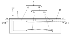
- the sensor substrate 1 includes an insulating substrate 2, a detection electrode 3 provided on the main surface (the upper surface in the example of FIG. 1) of the insulating substrate 2, and a resistance wiring 5 including an exothermic electrode 4 provided inside the insulating substrate 2. And have.
- the detection electrode 3 is externally connected by a wiring conductor that is a conductive path.
- the insulating substrate 2 has a flat plate shape such as a square plate shape, and is a base portion for providing the resistance wiring 5 including the detection electrode 3 and the heating electrode 4 in an electrically insulated manner.
- the insulating substrate 2 is made of a ceramic sintered body such as an aluminum oxide sintered body, an aluminum nitride sintered body, a mullite sintered body, a glass ceramic sintered body, a zirconia ceramic (zirconium oxide sintered body), or the like. Is formed.
- the insulating substrate 2 may be formed by laminating a plurality of insulating layers (no symbol) made of such a ceramic sintered body.
- the insulating substrate 2 is formed by laminating a plurality of insulating layers made of an aluminum oxide sintered body, for example, the insulating substrate 2 can be manufactured by the following method. First, an appropriate organic binder and solvent are added to and mixed with raw material powders such as aluminum oxide, silicon oxide, magnesium oxide and calcium oxide to form a slurry, which is then formed into a sheet by the doctor blade method or calendar roll method. Thus, a ceramic green sheet is obtained, a suitable punching process is performed on the ceramic green sheet, and a plurality of the ceramic green sheets are laminated as necessary, and fired at a high temperature (about 1400 to 1600 ° C.).
- a high temperature about 1400 to 1600 ° C.
- the detection electrode 3 is a part for measuring the content of fine particles such as soot in the environment where the sensor substrate 1 is disposed.
- fine particles such as soot adhere to the detection electrode 3
- the electrical resistance of the detection electrode 3 changes.
- the mass of the fine particles in the environment where the detection electrode 3 is present is calculated and detected.
- the content of the fine particles in the gas is calculated and detected.
- the detection electrode 3 contains a metal material that causes such a change in electrical resistance.
- this metal material contains a base metal material that is catalytically inactive (hereinafter simply referred to as “catalyst inactive”) as a main component for the decomposition reaction of the fine particles.
- the fine particles are, for example, soot (carbon fine particles).
- the base metal material which is the main component of the metal material can form the passive film on the surface of the detection electrode 3 (surface exposed to the outside). Examples of such base metal materials include materials containing iron, aluminum, nickel, titanium, chromium, silicon, and the like.
- the metal material of the detection electrode 3 is contained in, for example, about 80% by mass or more in the detection electrode 3 and is the main component of the detection electrode 3.
- the detection electrode 3 may contain an inorganic component such as glass or ceramic. These inorganic components are components for adjusting the firing shrinkage when the detection electrode 3 is formed by simultaneous firing with the insulating substrate 2 as described later, for example.
- the environment in which the sensor substrate 1 is disposed is, for example, an exhaust passage of an exhaust gas of an automobile. If the amount of fine particles detected by the sensor substrate 1 increases, it is detected that the content of fine particles flowing through the exhaust passage has increased. Thereby, for example, a failure of a DPF (Diesel Particulate Filter) that removes particulates such as soot from the exhaust gas can be detected.
- DPF Diesel Particulate Filter
- the detection electrode 3 has a length such as a linear pattern including a comb-like pattern or an elongated rectangular (band-like) pattern, for example. It is preferable that the pattern is formed in a pattern that can be easily lengthened.
- FIG. 1 shows an example in which the detection electrode 3 is an elongated rectangular pattern.
- the wiring conductor is formed on or in the upper surface of the insulating substrate 2 and is, for example, a conductive path for electrically connecting the detection electrode 3 on the upper surface of the insulating substrate 2 and a connection pad 7 on the upper surface described later.
- the wiring conductor is provided from the detection electrode 3 on the upper surface of the insulating substrate 2 to the main surface of the insulating substrate 2 on which the detection electrode 3 is provided. Thereby, the detection electrode 3 is electrically led out to the outer surface such as the upper surface of the insulating substrate 2.
- the connection pad 7 is provided on the lower surface of the insulating substrate 2, and the wiring conductor is provided on the other main surface (the lower surface in the example of FIG.
- the wiring conductor may include a through conductor that penetrates at least a part of the insulating substrate 2 in the thickness direction.
- the wiring conductor may include a circuit pattern shape provided between the insulating layers.
- connection pads 7 for external connection are provided on the upper surface of the insulating substrate 2.
- the connection pad 7 is directly connected to a portion of the wiring conductor that is electrically led to the upper surface of the insulating substrate 2.
- a wiring conductor is formed from the detection electrode 3 on the upper surface of the insulating substrate 2 to the connection pad 7 on the upper surface of the insulating substrate 2.
- This wiring conductor is for electrically connecting the detection electrode 3 and an external electric circuit (not shown). If the connection pad 7 is bonded to a predetermined part of the external electric circuit by a conductive bonding material such as solder or conductive adhesive, the detection electrode 3 and the external electric circuit are connected via the wiring conductor and the connection pad 7. Are electrically connected to each other.
- connection pad 7 is also provided on the lower surface of the insulating substrate 2, and the resistance wiring 5 including the heating electrode 4 is electrically connected to an external electric circuit via the connection pad 7. .
- an insulating layer 2 a made of the same material as that of the insulating substrate 2 may be provided on the main surface (upper surface) of the insulating substrate 2 so that the detection electrodes 3 and the connection pads 7 are exposed.
- the surface portion of the detection electrode 3 does not contain platinum, the catalytic action for the chemical reaction of the detected object such as soot oxidation is compared with the case where platinum is contained. It is effectively reduced. Therefore, oxidation of the detection object attached to the detection electrode is difficult to occur. Therefore, the sensor substrate 1 with high detection accuracy can be provided.
- the surface portion of the detection electrode 3 includes a passive film. Therefore, the possibility that the entire detection electrode 3 is oxidized is reduced. Therefore, the sensor substrate 1 with high detection accuracy and long-term reliability can be provided.
- the metal material contained in the detection electrode 3 is mainly composed of a base metal material containing at least one of iron, aluminum, nickel, titanium, chromium and silicon, which can easily form a passive film. These base metal materials are inactive to the catalyst and do not have a catalytic action for the decomposition of fine particles.
- the metal material forming the detection electrode 3 contains, for example, at least one such base metal material in a proportion of about 80% by mass or more.
- the metal material may contain other metal components.
- the other metal material does not necessarily need to be a metal material that easily forms a passive film, and may be another metal material (for example, tungsten).
- the detection electrode 3 is formed as follows, for example. That is, the above base metal material powder is kneaded with an organic solvent and a binder to produce a metal paste, and this metal paste is applied to the main surface of the ceramic green sheet to be the insulating substrate 2 in a predetermined pattern.
- the metal paste is applied by, for example, a screen printing method. Thereafter, these metal paste and ceramic green sheet are fired simultaneously.
- the insulating substrate 2 having the detection electrode 3 can be manufactured by the above process.
- the thickness of the passive film is set to about 0.1 to 5 ⁇ m, for example. With such a thickness, the surface portion of the detection electrode 3 is effectively covered with a passive film, and the possibility that the whole or most of the surface electrode is oxidized is effectively reduced.
- the surface portion of the detection electrode 3 includes a passive film in an area ratio of about 90%. In other words, it is preferable that 90% or more of the exposed surface of the detection electrode 3 is covered with the passive film. Thereby, the possibility that the oxidation proceeds to the entire detection electrode 3 is effectively reduced.
- the entire surface portion of the detection electrode 3 includes a passive film.
- the entire exposed surface of the detection electrode 3 is covered with a passive film.
- the passive film If the passive film is too thick, the initial resistance of the surface portion of the detection electrode 3 (resistance before being set in an environment containing fine particles) increases, and the change in the resistance value of the detection electrode 3 due to adhesion of the fine particles. Is difficult to detect.
- the above baking may be performed in an atmosphere containing a small amount of oxygen and moisture.
- a passive film is formed on the exposed surface of the metal material including the base metal material.
- the passive film is an oxide layer containing at least one of iron oxide, chromium oxide, and chromium oxide when the detection electrode 3 is an object containing an iron-nickel-chromium alloy as a main component.
- the presence of the passive film on the surface portion suppresses the oxidation from proceeding to the iron-nickel-chromium alloy existing inside the passive film of the detection electrode 3.
- the metal material forming the passive film preferably contains an iron-nickel-chromium alloy as a main component. That is, the base metal material is preferably an iron-nickel-chromium alloy. This is due to the following reason. That is, the passive film containing such a base metal material is formed by oxidation of a metal material containing iron, nickel, and chromium. For that purpose, the metal material contained in the detection electrode 3 contains iron, nickel, and chromium. These metal materials can easily form the detection electrode 3 by co-firing with the insulating substrate 2 (ceramic green sheet) as a metal paste as described above, for example. Moreover, it is easy to form a passive film, and the progress of oxidation to the inside of the detection electrode 3 is more effectively suppressed. Further, these base metals are catalytically inactive metals that do not have a catalytic action.
- the metal material forming the detection electrode 3 is composed mainly of iron-nickel-chromium.
- the alloy material is preferably as follows.
- a metal material containing an iron-nickel-chromium alloy as a base metal material as a main component for example, iron (Fe) 1 to 55 mass%, nickel (Ni) 20 to 80 mass%, chromium ( Cr) is 10 to 25% by mass, titanium (Ti) is 0.1 to 5% by mass, and aluminum (Ai) is 0.1 to 5% by mass.
- the base metal material that is the main component of the metal material forming the passive film may contain iron and chromium.
- a passive film containing a base metal material is formed by oxidation of a metal material containing iron and chromium, and the metal material contained in the detection electrode 3 contains iron and chromium.
- the metal material contained in the detection electrode 3 contains iron and chromium.
- it is easy to form a passive film and the progress of oxidation to the inside of the detection electrode 3 is more effectively suppressed.
- these base metals are catalytically inactive metals that do not have a catalytic action.
- the metal material forming the detection electrode 3 is composed mainly of iron-chromium. It may be an alloy material.
- the iron-chromium alloy can also be regarded as a nickel component removed from the iron-nickel-chromium alloy described above. Since the iron-chromium alloy is easier to passivate than the iron-nickel-chromium alloy, it is easier to form a passive film on the surface portion of the detection electrode 3.
- the passive film should just be provided in the surface part exposed in environments, such as the external air of the detection electrode 3.
- FIG. A passivation film is not necessarily provided on the surface portion of the detection electrode 3 that is in contact with the insulating substrate 2.
- the passive film is cut at the portion where the detection electrode 3 is provided so that the sensor substrate 1 can be viewed in a longitudinal section, and the surface portion of the detection electrode 3 is analyzed by electron beam microanalyzer (EPMA) or X-ray diffraction analysis. It can detect by analyzing by the method of etc. Also, the thickness of the passive film can be measured by this method.
- EPMA electron beam microanalyzer
- X-ray diffraction analysis It can detect by analyzing by the method of etc.
- the thickness of the passive film can be measured by this method.
- the wiring conductor is made of, for example, the same metal material as that of the detection electrode 3, and may have a passive film (not shown) on the surface thereof. Further, the wiring conductor may be made of a metal that is difficult to oxidize, such as platinum or gold.
- connection pad 7 can also be manufactured by the same method using, for example, the same metal material as that of the detection electrode 3. However, if only the detection electrode 3 and its periphery (for example, the upper surface of the insulating substrate 2) of the sensor substrate 1 are exposed and used in the flow path of the gas containing fine particles, the connection pad 7 is The metal material that easily forms the passive film as described above may not be included. That is, in such a case, since the connection pad 7 is less likely to be oxidized by a high-temperature gas or the like, it does not necessarily have to have oxidation resistance like the detection electrode 3.
- the wiring conductor and the connection pad 7 may be made of a metal material having a catalytic action, or made of other metal materials It does not matter either. That is, the wiring conductor and the connection pad 7 may be, for example, tungsten, manganese, cobalt, copper, gold, or an alloy containing these metal materials (for example, nickel-cobalt alloy).
- the wiring conductor and the connection pad 7 for example, considering the ease of formation by simultaneous firing with the insulating substrate 2 made of an aluminum oxide sintered body, the strength of bonding to the insulating substrate 2, and characteristics such as electrical resistance, What contains tungsten as a main component may be used.
- a plating layer such as nickel and gold may be applied to the exposed surface of the connection pad 7.
- oxidation of the connection pad 7, suppression of corrosion, and improvement of characteristics such as wettability of solder connecting the connection pad 7 and the external electric circuit can be achieved. Improve.
- the detection electrode 3 may be made of a metal material whose main component is molybdenum silicide (for example, MoSi 2 ). In this case, molybdenum silicide is the base metal material.
- the detection electrode 3 may contain an iron-nickel-chromium alloy and molybdenum silicide as main components.
- the glass component described above when the glass component described above is contained in the detection electrode 3, it is difficult for the glass component to enter between the iron-nickel-chromium particles and the molybdenum silicide particles. Therefore, oversintering due to penetration of the glass component between the particles is less likely to occur. Thereby, the oxidation resistance of the detection electrode 3 is further improved.
- the detection electrode 3 contains molybdenum silicide
- the content is set to about 90 to 100% by mass, for example. As a result, the above effect can be obtained more reliably.
- the heating electrode 4 is included in the resistance wiring 5, and is provided in the insulating substrate 2 at a position corresponding to the detection electrode 3, for example, a position overlapping the detection electrode 3 in a plan view.
- a voltage is applied to the resistance wiring 5 including the heat generating electrode 4 to heat the heat generating electrode 4 and fine particles such as soot adhering to the detection electrode 3 can be decomposed.
- the heating electrode 4 is provided at a position closest to the detection electrode 3 in the resistance wiring 5, when a voltage is applied to the resistance wiring 5 including the heating electrode 4 to cause the heating electrode 4 to generate heat, Fine particles such as soot that are effectively transferred and adhered to the detection electrode 3 can be decomposed better.
- the width of the heating electrode 4 is smaller than the width of the wiring 8a and the width of the other wiring 8b in the multilayer wiring portion 8 described later. Such a configuration is preferable because a voltage can be applied to the resistance wiring 5 including the heat generating electrode 4 and the heat generating electrode 4 can be efficiently heated.
- the heating electrode 4 is made of, for example, the same metal material as that of the detection electrode 3 and includes a material containing iron, titanium, chromium, silicon and the like having a high electrical resistivity in order to generate heat particularly efficiently. Further, the heating electrode 4 may contain, as a main component, a metal that hardly oxidizes, such as platinum or iron-nickel-chromium alloy.
- the metal material of the heating electrode 4 is, for example, contained in the heating electrode 4 in an amount of about 80% by mass or more, and is a main component of the heating electrode 4.
- the heating electrode 4 may contain an inorganic component such as glass or ceramic in addition to the metal material. These inorganic components are components for adjusting the firing shrinkage when the heating electrode 4 is formed by simultaneous firing with the insulating substrate 2, for example.
- iron-nickel-chromium alloy for example, iron (Fe) 1 to 55% by mass, nickel (Ni) 20 to 80% by mass, chromium, as with the detection electrode 3
- iron (Fe) 1 to 55% by mass, nickel (Ni) 20 to 80% by mass, chromium as with the detection electrode 3
- iron (Fe) 1 to 55% by mass, nickel (Ni) 20 to 80% by mass, chromium as with the detection electrode 3
- examples thereof include (Cr) of 10 to 25% by mass, titanium (Ti) of 0.1 to 5% by mass and aluminum (Ai) of 0.1 to 5% by mass.
- the heating electrode 4 is formed in the same manner as the detection electrode 3, for example. That is, a metal paste is prepared by kneading the metal material powder for the heating electrode 4 together with an organic solvent and a binder, and the metal paste is formed in a predetermined pattern on the main surface of the ceramic green sheet to be the insulating substrate 2. Apply. The metal paste is applied by, for example, a screen printing method. Thereafter, if necessary, a plurality of ceramic green sheets are laminated, and the metal paste and the ceramic green sheets are fired simultaneously.
- the insulating substrate 2 having the heating electrode 4 can be manufactured through the above steps.
- the resistance wiring 5 is provided inside the insulating substrate 2 and is connected to the heating electrode 4 and has a multilayer wiring portion 8 in which a wiring 8a and another wiring 8b are connected in parallel. With such a configuration, the resistance wiring 5 has a portion in which the electrical resistivity of the resistance wiring 5 is suppressed by the multilayer wiring portion 8, and a voltage is applied to the resistance wiring 5 including the heating electrode 4. When applied, the heating electrode 4 can be heated without increasing the voltage applied to the resistance wiring 5, so that fine particles such as soot adhering to the detection electrode 3 can be decomposed, and the detection accuracy is improved. It becomes possible.
- the resistance wiring 5 may be exposed on the other main surface (lower surface) of the insulating substrate 2.
- the multilayer wiring portion 8 may include a through conductor that penetrates at least a part of the insulating substrate 2 in the thickness direction.
- the wiring 8a and the other wiring 8b are connected in parallel via the through conductor.
- connection pads 7 for external connection are provided on the lower surface of the insulating substrate 2.
- the connection pad 7 is directly connected to a portion of the multilayer wiring portion 8 that is electrically led to the lower surface of the insulating substrate 2.
- the resistance wiring 5 is formed from the inside of the insulating substrate 2 (the heat generating electrode 4) to the connection pad 7 on the lower surface of the insulating substrate 2.
- the connection pad 7 is bonded to a predetermined portion of the external electric circuit by a conductive bonding material such as solder or a conductive adhesive, and the heating electrode 4 and the external electric circuit are electrically connected to each other.
- the multilayer wiring part 8 is made of, for example, the same metal material as that of the heat generating electrode 4, and particularly includes a material containing iron, titanium, chromium, silicon and the like. Further, the multilayer wiring portion 8 may contain a metal which is difficult to oxidize such as platinum or iron-nickel-chromium alloy as a main component.
- the metal material of the multilayer wiring part 8 is, for example, contained in the multilayer wiring part 8 by about 80% by mass or more and is a main component of the multilayer wiring part 8.
- the multilayer wiring portion 8 may contain an inorganic component such as glass or ceramic in addition to the metal material. These inorganic components are components for adjusting the firing shrinkage when the multilayer wiring portion 8 is formed by simultaneous firing with the insulating substrate 2, for example.
- iron-nickel-chromium alloy is contained as the metal material of the multilayer wiring portion 8, for example, iron (Fe) 1-55 mass%, nickel (Ni) 20-80 mass%, Examples include chromium (Cr) of 10 to 25% by mass, titanium (Ti) of 0.1 to 5% by mass and aluminum (Ai) of 0.1 to 5% by mass.
- the multilayer wiring portion 8 is formed in the same manner as the heating electrode 4, for example. That is, the metal material powder for the multilayer wiring portion 8 is kneaded with an organic solvent and a binder to produce a metal paste, and this metal paste is applied to the main surface of the ceramic green sheet to be the insulating substrate 2 and the like on the wiring 8a. And it apply
- the metal paste is applied by, for example, a screen printing method. Thereafter, if necessary, a plurality of ceramic green sheets are laminated, and the metal paste and the ceramic green sheets are fired simultaneously. Through the above steps, the insulating substrate 2 having the multilayer wiring portion 8 can be manufactured.
- wiring 8 a and other wiring 8 b are provided in multiple layers in the thickness direction of the insulating substrate 2 via an insulating layer. With such a configuration, the wiring 8a and the other wiring 8b connected in parallel do not have a large configuration in the planar direction of the insulating substrate 2, and the sensor substrate 1 that suppresses an increase in outer shape is provided. can do.
- the width of the wiring 8a or the other wiring 8b is gradually narrowed from the end connected to the heating electrode 4 to the other end.
- the thermal resistance of the wiring 8a or the other wiring 8b can be increased, and when the heating electrode 4 is heated by applying a voltage to the resistance wiring 5 including the heating electrode 4, Heat loss can be suppressed.
- the width W1 of the other end of the wiring 8a or the other wiring 8b is larger than the width W2 of the heating electrode 4, a voltage is applied to the resistance wiring 5 including the heating electrode 4 to cause the heating electrode 4 to generate heat. In this case, heat loss can be effectively suppressed.
- the width gradually decreases from the end connected to the heating electrode 4 to the other end, and the width W1 of the other end in the wiring 8a is the heating electrode 4. It is larger than the width W2.
- the wiring 8a and the other wiring 8b are adjacent to each other in the thickness direction of the insulating substrate 2, and are arranged so as not to overlap each other in plan perspective.
- the other wiring 8b is arranged so as to be sandwiched between the wirings 8a in a plan view.
- the size of the heat generating electrode 4 can be easily increased in a plan view.
- the heating electrode 4 is heated by applying a voltage to 5, the heat generation area becomes large and fine particles such as soot adhering to the detection electrode 3 can be decomposed satisfactorily.
- the wiring 8 a and the other wiring 8 b are arranged so as to have a portion sandwiched between each other in plan perspective.
- the heating electrode 4 connected to the wiring 8a or the other wiring 8b is disposed in a region including the central portion of the insulating substrate 2 in a plan view, and the heating electrode 4 in a plan view.
- a comb-teeth portion that has an influence on the detection characteristics of the detection electrode 3 that is a comb-shaped pattern overlaps, and a voltage is applied to the resistance wiring 5 including the heating electrode 4 to generate heat.
- fine particles such as soot adhering to the detection electrode 3 can be decomposed better.
- the sensor device 10 of the embodiment is formed by the sensor substrate 1 having the above-described configuration and the power supply unit 11 that supplies a potential to the resistance wiring 5 including the detection electrode 3 and the heating electrode 4.
- Different electrodes (positive electrode, negative electrode, etc.) of the power supply unit 11 are connected to different lead terminals 9.
- a potential of about 50 volts (V) is supplied from the power supply unit 11 to the detection electrode 3, and a leakage current due to this potential is detected.
- the resistance value of the detection electrode 3 is detected by the value of this leakage current.
- the resistance value of the detection electrode 3 is measured by, for example, an external measurement detection circuit (not shown). Further, a circuit for measuring the resistance value of the detection electrode 3 (not shown) may be disposed on the insulating substrate 2.
- the power supply unit 11 is, for example, a terminal, a rectifier, a transformer circuit, and the like that are electrically connected to an external power supply (not shown) as a soot detection circuit, and is a part to which predetermined power is transmitted from the external power supply.
- the transmitted power is adjusted to a condition suitable for measuring the resistance value of the detection electrode 3 in the power supply unit 11 and transmitted to the detection electrode 3.
- connection conductor such as a conductive connection material that electrically connects the connection pad 7 and the power supply unit 11 is schematically shown by a virtual line (two-dot chain line).
- the detection accuracy is high.
- the detection electrode 3 is made of platinum and the temperature of the atmosphere (exhaust gas) in which soot is detected as fine particles is about 550 ° C., soot is decomposed by the catalytic reaction of platinum, Soot is not detected effectively.
- the detection electrode 3 since the detection electrode 3 is inactive to the catalyst, soot decomposition is suppressed and the content of soot as fine particles is detected with high accuracy.
- FIG. 5A is a top view showing a modified example of the sensor substrate and the sensor device shown in FIG. 1
- FIG. 5B is a cross-sectional view showing another modified example of the sensor substrate and the sensor device shown in FIG. is there. 5, parts similar to those in FIG. 1 are denoted by the same reference numerals.
- the detection electrode 3 has a comb-like pattern. Further, the two detection electrodes 3 are arranged in such a positional relationship as to engage with each other. In this case, for example, the length of the detection electrode 3 can be increased while keeping the size of the insulating substrate 2 in plan view as small as possible. As the length of the detection electrode 3 is longer, the change in the resistance value as the detection electrode 3 tends to increase. In addition, detection of fine particles in the gas becomes easy. That is, even when the content of fine particles in the gas is small, the fine particles can be detected more reliably.
- the sensor substrate 1 and the sensor device 10 that are more advantageous in terms of improvement in accuracy and sensitivity of detection of fine particles in the gas and miniaturization in plan view.
- a conductor such as a connection pad for electrical connection between the power supply unit 11 and the detection electrode 3 is schematically shown by a virtual line (two-dot chain line).
- the lead terminal 9 is joined to the connection pad 7.
- the end of the lead terminal 9 opposite to the end joined to the connection pad 7 is joined to a predetermined part of the external electric circuit and electrically connected. That is, electrical and mechanical connection to the external electric circuit of the sensor substrate 1 (sensor device 10) is performed via the lead terminals 9.
- Different electrodes (positive electrode, negative electrode, etc.) of the power supply unit 11 are connected to different lead terminals 9.
- the insulating substrate 2 of the sensor substrate 1 and the external electric circuit are provided by elastic deformation of the lead terminal 9.
- the lead terminal 9 is not for detecting fine particles, like the connection pad 7. Therefore, the material for forming the lead terminals 9 may be appropriately selected according to the environment in which the lead terminals 9 are used, the conditions such as the productivity and economy of the sensor substrate 1. For example, if the lead terminal 9 is made of a metal material having excellent oxidation resistance such as platinum or gold, it is advantageous in terms of reliability as the sensor device 10. Further, the lead terminal 9 may be formed of an iron-based alloy such as an iron-nickel-cobalt alloy, copper, or the like with emphasis on economy and the like. Further, when the lead terminal 9 is made of an iron-based alloy, the exposed surface may be protected by a plating layer such as a gold plating layer.
- a plating layer such as a gold plating layer.
- the bonding of the lead terminals 9 to the connection pads 7 is performed by, for example, a brazing material (no symbol) such as silver brazing (silver copper brazing material) or gold brazing.
- a brazing material such as silver brazing (silver copper brazing material) or gold brazing.
- the brazing material as with the lead terminal 9, the material is appropriately selected according to various conditions when the sensor substrate 1 is manufactured or used.
- the sensor substrate and the sensor device of the present invention are not limited to the above-described embodiments, and various modifications are possible within the scope of the gist of the present invention.
Landscapes
- Chemical & Material Sciences (AREA)
- Biochemistry (AREA)
- Physics & Mathematics (AREA)
- Health & Medical Sciences (AREA)
- Life Sciences & Earth Sciences (AREA)
- Analytical Chemistry (AREA)
- General Health & Medical Sciences (AREA)
- General Physics & Mathematics (AREA)
- Immunology (AREA)
- Pathology (AREA)
- Dispersion Chemistry (AREA)
- Chemical Kinetics & Catalysis (AREA)
- Electrochemistry (AREA)
- Investigating Or Analyzing Materials By The Use Of Electric Means (AREA)
Abstract
Description
Claims (8)
- 絶縁基板と、
該絶縁基板の主面に設けられた検知電極と、
前記絶縁基板の内部に設けられ、発熱電極を含む抵抗配線とを有しており、
該抵抗配線は、前記発熱電極に接続され、配線および他の配線が並列に接続された多層配線部を有していることを特徴とするセンサ基板。 - 前記多層配線部は、前記配線および前記他の配線が前記絶縁基板の厚み方向に多層に設けられていることを特徴とする請求項1に記載のセンサ基板。
- 前記配線または前記他の配線は、前記発熱電極に接続された端部から他の端部にかけて幅が漸次狭くなっていることを特徴とする請求項1または請求項2に記載のセンサ基板。
- 前記配線および前記他の配線は、前記絶縁基板の厚み方向において隣接しており、平面透視で互いに重ならないように配置されていることを特徴とする請求項1乃至請求項3のいずれかに記載のセンサ基板。
- 平面透視において、前記他の配線が前記配線に挟まれるように配置されていることを特徴とする請求項4に記載のセンサ基板。
- 平面透視において、前記配線と前記他の配線とが互いに挟まれる部分を有するように配置されていることを特徴とする請求項4に記載のセンサ基板。
- 前記検知電極は、くし歯状のパターンであり、互いにかみ合うように配置されていることを特徴とする請求項1乃至請求項6のいずれかに記載のセンサ基板。
- 請求項1乃至請求項7のいずれかに記載のセンサ基板と、
前記発熱電極に電位を供給する電源部とを有していることを特徴とするセンサ装置。
Priority Applications (4)
| Application Number | Priority Date | Filing Date | Title |
|---|---|---|---|
| EP16830488.9A EP3330702B1 (en) | 2015-07-28 | 2016-07-25 | Sensor substrate and sensor device |
| US15/554,108 US10338019B2 (en) | 2015-07-28 | 2016-07-25 | Sensor substrate and sensor device |
| CN201680009483.9A CN107209135B (zh) | 2015-07-28 | 2016-07-25 | 传感器基板以及传感器装置 |
| JP2017530860A JP6462882B2 (ja) | 2015-07-28 | 2016-07-25 | センサ基板およびセンサ装置 |
Applications Claiming Priority (2)
| Application Number | Priority Date | Filing Date | Title |
|---|---|---|---|
| JP2015148711 | 2015-07-28 | ||
| JP2015-148711 | 2015-07-28 |
Publications (1)
| Publication Number | Publication Date |
|---|---|
| WO2017018383A1 true WO2017018383A1 (ja) | 2017-02-02 |
Family
ID=57884345
Family Applications (1)
| Application Number | Title | Priority Date | Filing Date |
|---|---|---|---|
| PCT/JP2016/071741 Ceased WO2017018383A1 (ja) | 2015-07-28 | 2016-07-25 | センサ基板およびセンサ装置 |
Country Status (5)
| Country | Link |
|---|---|
| US (1) | US10338019B2 (ja) |
| EP (1) | EP3330702B1 (ja) |
| JP (1) | JP6462882B2 (ja) |
| CN (1) | CN107209135B (ja) |
| WO (1) | WO2017018383A1 (ja) |
Families Citing this family (7)
| Publication number | Priority date | Publication date | Assignee | Title |
|---|---|---|---|---|
| US10768131B2 (en) * | 2015-11-25 | 2020-09-08 | Kyocera Corporation | Sensor substrate arrangement for a particulate sensor device |
| JP2020034349A (ja) * | 2018-08-28 | 2020-03-05 | イビデン株式会社 | 粒子状物質検出センサ素子 |
| JP2020034348A (ja) * | 2018-08-28 | 2020-03-05 | イビデン株式会社 | 粒子状物質検出センサ素子 |
| JP7285056B2 (ja) * | 2018-09-21 | 2023-06-01 | Koa株式会社 | 流量センサ装置 |
| CN109324219B (zh) * | 2018-11-28 | 2024-07-12 | 钧崴电子科技股份有限公司 | 短电极四端子电流感测组件及其生产工艺 |
| JP7373353B2 (ja) * | 2019-10-16 | 2023-11-02 | 株式会社Kelk | 熱電モジュール、及び熱電モジュール用ポストの製造方法 |
| CN112965116A (zh) * | 2021-03-29 | 2021-06-15 | 上海和辉光电股份有限公司 | 一种涂布中检知基板金属异物的装置 |
Citations (6)
| Publication number | Priority date | Publication date | Assignee | Title |
|---|---|---|---|---|
| JPS59225587A (ja) * | 1983-06-06 | 1984-12-18 | 株式会社日立製作所 | セラミツク配線基板 |
| JPH10267895A (ja) * | 1997-03-26 | 1998-10-09 | Ngk Spark Plug Co Ltd | 排気ガスセンサ及びそれを用いた排気ガスセンサシステム |
| JPH11312737A (ja) * | 1998-04-28 | 1999-11-09 | Sanyo Electric Co Ltd | 集積回路 |
| JP2007024538A (ja) * | 2005-07-12 | 2007-02-01 | Yamaha Motor Co Ltd | ガス検出装置の温度制御装置ならびにそれを備える空燃比制御装置及び内燃機関 |
| JP2011226832A (ja) * | 2010-04-16 | 2011-11-10 | Ngk Insulators Ltd | 粒子状物質検出装置 |
| JP2012078130A (ja) * | 2010-09-30 | 2012-04-19 | Denso Corp | 粒子状物質検出センサおよびその製造方法 |
Family Cites Families (11)
| Publication number | Priority date | Publication date | Assignee | Title |
|---|---|---|---|---|
| US3839660A (en) * | 1973-02-05 | 1974-10-01 | Gen Motors Corp | Power semiconductor device package |
| DE2836002C2 (de) | 1978-08-17 | 1986-09-11 | Robert Bosch Gmbh, 7000 Stuttgart | Sensor zur Überwachung der Rußfreiheit von Abgasen |
| JPS59197847A (ja) | 1983-04-25 | 1984-11-09 | Ngk Spark Plug Co Ltd | スモーク濃度センサ |
| US4785243A (en) * | 1987-01-29 | 1988-11-15 | Ltv Steel Company | Electronically scanned eddy current flaw inspection |
| US5766780A (en) * | 1996-10-15 | 1998-06-16 | Seagate Technology, Inc. | Reversed order NIMN exchange biasing for dual magnetoresistive heads |
| US7352191B2 (en) * | 2005-04-04 | 2008-04-01 | 3M Innovative Properties Company | Sensor assembly and method of forming the same |
| US20090056416A1 (en) * | 2007-08-30 | 2009-03-05 | Nair Balakrishnan G | Ceramic Particulate Matter Sensor With Low Electrical Leakage |
| JP5635776B2 (ja) * | 2010-01-07 | 2014-12-03 | 日本碍子株式会社 | 粒子状物質検出装置、及び粒子状物質検出装置の検査方法 |
| US9681996B2 (en) * | 2011-08-11 | 2017-06-20 | 3M Innovative Properties Company | Wetness sensors |
| CN104271322B (zh) * | 2012-03-08 | 2016-09-21 | 品质制造有限公司 | 触敏机器人抓手 |
| JP5984505B2 (ja) * | 2012-05-22 | 2016-09-06 | 株式会社日立製作所 | 半導体ガスセンサおよびその製造方法 |
-
2016
- 2016-07-25 CN CN201680009483.9A patent/CN107209135B/zh active Active
- 2016-07-25 US US15/554,108 patent/US10338019B2/en active Active
- 2016-07-25 WO PCT/JP2016/071741 patent/WO2017018383A1/ja not_active Ceased
- 2016-07-25 JP JP2017530860A patent/JP6462882B2/ja active Active
- 2016-07-25 EP EP16830488.9A patent/EP3330702B1/en active Active
Patent Citations (6)
| Publication number | Priority date | Publication date | Assignee | Title |
|---|---|---|---|---|
| JPS59225587A (ja) * | 1983-06-06 | 1984-12-18 | 株式会社日立製作所 | セラミツク配線基板 |
| JPH10267895A (ja) * | 1997-03-26 | 1998-10-09 | Ngk Spark Plug Co Ltd | 排気ガスセンサ及びそれを用いた排気ガスセンサシステム |
| JPH11312737A (ja) * | 1998-04-28 | 1999-11-09 | Sanyo Electric Co Ltd | 集積回路 |
| JP2007024538A (ja) * | 2005-07-12 | 2007-02-01 | Yamaha Motor Co Ltd | ガス検出装置の温度制御装置ならびにそれを備える空燃比制御装置及び内燃機関 |
| JP2011226832A (ja) * | 2010-04-16 | 2011-11-10 | Ngk Insulators Ltd | 粒子状物質検出装置 |
| JP2012078130A (ja) * | 2010-09-30 | 2012-04-19 | Denso Corp | 粒子状物質検出センサおよびその製造方法 |
Non-Patent Citations (1)
| Title |
|---|
| See also references of EP3330702A4 * |
Also Published As
| Publication number | Publication date |
|---|---|
| US10338019B2 (en) | 2019-07-02 |
| CN107209135A (zh) | 2017-09-26 |
| EP3330702B1 (en) | 2020-05-27 |
| JPWO2017018383A1 (ja) | 2017-11-16 |
| CN107209135B (zh) | 2019-10-01 |
| US20180052128A1 (en) | 2018-02-22 |
| EP3330702A4 (en) | 2019-03-13 |
| EP3330702A1 (en) | 2018-06-06 |
| JP6462882B2 (ja) | 2019-01-30 |
Similar Documents
| Publication | Publication Date | Title |
|---|---|---|
| JP6462882B2 (ja) | センサ基板およびセンサ装置 | |
| JP6272492B2 (ja) | センサ基板、リード付きセンサ基板およびセンサ装置 | |
| JP5634433B2 (ja) | 粒子状物質検出素子とその製造方法、並びに、粒子状物質検出センサ | |
| JP2012058015A (ja) | 粒子状物質検出装置 | |
| CN106574872A (zh) | 传感器元件、传感器装置和用于制造传感器元件的方法 | |
| JP6674842B2 (ja) | センサ基板およびセンサ装置 | |
| JP6957616B2 (ja) | センサ基板およびセンサ装置 | |
| JP6368855B2 (ja) | センサ基板およびセンサ装置 | |
| CN108369845B (zh) | 热敏电阻及使用热敏电阻的装置 | |
| JP6462408B2 (ja) | センサ基板および検出装置 | |
| CN112567235A (zh) | 颗粒状物质检测传感器元件 | |
| JP4480608B2 (ja) | 配線基板 | |
| JP2016085132A (ja) | センサ基板およびセンサ装置 | |
| JP6923657B2 (ja) | センサ基板およびそれを備えるセンサ装置 | |
| WO2020045049A1 (ja) | 粒子状物質検出センサ素子 | |
| JP2012079976A (ja) | 薄膜サーミスタ | |
| JP4471765B2 (ja) | 配線基板およびその製造方法 | |
| JP4484650B2 (ja) | 配線基板 |
Legal Events
| Date | Code | Title | Description |
|---|---|---|---|
| 121 | Ep: the epo has been informed by wipo that ep was designated in this application |
Ref document number: 16830488 Country of ref document: EP Kind code of ref document: A1 |
|
| ENP | Entry into the national phase |
Ref document number: 2017530860 Country of ref document: JP Kind code of ref document: A |
|
| REEP | Request for entry into the european phase |
Ref document number: 2016830488 Country of ref document: EP |
|
| WWE | Wipo information: entry into national phase |
Ref document number: 15554108 Country of ref document: US |
|
| NENP | Non-entry into the national phase |
Ref country code: DE |