WO2017018834A1 - Procédé de fabrication d'un film mince de dichalcogénure de métal de transition à deux dimensions - Google Patents
Procédé de fabrication d'un film mince de dichalcogénure de métal de transition à deux dimensions Download PDFInfo
- Publication number
- WO2017018834A1 WO2017018834A1 PCT/KR2016/008303 KR2016008303W WO2017018834A1 WO 2017018834 A1 WO2017018834 A1 WO 2017018834A1 KR 2016008303 W KR2016008303 W KR 2016008303W WO 2017018834 A1 WO2017018834 A1 WO 2017018834A1
- Authority
- WO
- WIPO (PCT)
- Prior art keywords
- transition metal
- substrate
- containing precursor
- dimensional
- chalcogen
- Prior art date
- Legal status (The legal status is an assumption and is not a legal conclusion. Google has not performed a legal analysis and makes no representation as to the accuracy of the status listed.)
- Ceased
Links
Images


Classifications
-
- C—CHEMISTRY; METALLURGY
- C23—COATING METALLIC MATERIAL; COATING MATERIAL WITH METALLIC MATERIAL; CHEMICAL SURFACE TREATMENT; DIFFUSION TREATMENT OF METALLIC MATERIAL; COATING BY VACUUM EVAPORATION, BY SPUTTERING, BY ION IMPLANTATION OR BY CHEMICAL VAPOUR DEPOSITION, IN GENERAL; INHIBITING CORROSION OF METALLIC MATERIAL OR INCRUSTATION IN GENERAL
- C23C—COATING METALLIC MATERIAL; COATING MATERIAL WITH METALLIC MATERIAL; SURFACE TREATMENT OF METALLIC MATERIAL BY DIFFUSION INTO THE SURFACE, BY CHEMICAL CONVERSION OR SUBSTITUTION; COATING BY VACUUM EVAPORATION, BY SPUTTERING, BY ION IMPLANTATION OR BY CHEMICAL VAPOUR DEPOSITION, IN GENERAL
- C23C16/00—Chemical coating by decomposition of gaseous compounds, without leaving reaction products of surface material in the coating, i.e. chemical vapour deposition [CVD] processes
- C23C16/22—Chemical coating by decomposition of gaseous compounds, without leaving reaction products of surface material in the coating, i.e. chemical vapour deposition [CVD] processes characterised by the deposition of inorganic material, other than metallic material
- C23C16/30—Deposition of compounds, mixtures or solid solutions, e.g. borides, carbides, nitrides
- C23C16/305—Sulfides, selenides, or tellurides
-
- C—CHEMISTRY; METALLURGY
- C01—INORGANIC CHEMISTRY
- C01B—NON-METALLIC ELEMENTS; COMPOUNDS THEREOF; METALLOIDS OR COMPOUNDS THEREOF NOT COVERED BY SUBCLASS C01C
- C01B17/00—Sulfur; Compounds thereof
- C01B17/20—Methods for preparing sulfides or polysulfides, in general
-
- C—CHEMISTRY; METALLURGY
- C01—INORGANIC CHEMISTRY
- C01G—COMPOUNDS CONTAINING METALS NOT COVERED BY SUBCLASSES C01D OR C01F
- C01G39/00—Compounds of molybdenum
- C01G39/06—Sulfides
-
- C—CHEMISTRY; METALLURGY
- C23—COATING METALLIC MATERIAL; COATING MATERIAL WITH METALLIC MATERIAL; CHEMICAL SURFACE TREATMENT; DIFFUSION TREATMENT OF METALLIC MATERIAL; COATING BY VACUUM EVAPORATION, BY SPUTTERING, BY ION IMPLANTATION OR BY CHEMICAL VAPOUR DEPOSITION, IN GENERAL; INHIBITING CORROSION OF METALLIC MATERIAL OR INCRUSTATION IN GENERAL
- C23C—COATING METALLIC MATERIAL; COATING MATERIAL WITH METALLIC MATERIAL; SURFACE TREATMENT OF METALLIC MATERIAL BY DIFFUSION INTO THE SURFACE, BY CHEMICAL CONVERSION OR SUBSTITUTION; COATING BY VACUUM EVAPORATION, BY SPUTTERING, BY ION IMPLANTATION OR BY CHEMICAL VAPOUR DEPOSITION, IN GENERAL
- C23C16/00—Chemical coating by decomposition of gaseous compounds, without leaving reaction products of surface material in the coating, i.e. chemical vapour deposition [CVD] processes
- C23C16/02—Pretreatment of the material to be coated
- C23C16/0227—Pretreatment of the material to be coated by cleaning or etching
-
- C—CHEMISTRY; METALLURGY
- C23—COATING METALLIC MATERIAL; COATING MATERIAL WITH METALLIC MATERIAL; CHEMICAL SURFACE TREATMENT; DIFFUSION TREATMENT OF METALLIC MATERIAL; COATING BY VACUUM EVAPORATION, BY SPUTTERING, BY ION IMPLANTATION OR BY CHEMICAL VAPOUR DEPOSITION, IN GENERAL; INHIBITING CORROSION OF METALLIC MATERIAL OR INCRUSTATION IN GENERAL
- C23C—COATING METALLIC MATERIAL; COATING MATERIAL WITH METALLIC MATERIAL; SURFACE TREATMENT OF METALLIC MATERIAL BY DIFFUSION INTO THE SURFACE, BY CHEMICAL CONVERSION OR SUBSTITUTION; COATING BY VACUUM EVAPORATION, BY SPUTTERING, BY ION IMPLANTATION OR BY CHEMICAL VAPOUR DEPOSITION, IN GENERAL
- C23C16/00—Chemical coating by decomposition of gaseous compounds, without leaving reaction products of surface material in the coating, i.e. chemical vapour deposition [CVD] processes
- C23C16/44—Chemical coating by decomposition of gaseous compounds, without leaving reaction products of surface material in the coating, i.e. chemical vapour deposition [CVD] processes characterised by the method of coating
- C23C16/455—Chemical coating by decomposition of gaseous compounds, without leaving reaction products of surface material in the coating, i.e. chemical vapour deposition [CVD] processes characterised by the method of coating characterised by the method used for introducing gases into reaction chamber or for modifying gas flows in reaction chamber
- C23C16/45523—Pulsed gas flow or change of composition over time
- C23C16/45525—Atomic layer deposition [ALD]
- C23C16/45527—Atomic layer deposition [ALD] characterized by the ALD cycle, e.g. different flows or temperatures during half-reactions, unusual pulsing sequence, use of precursor mixtures or auxiliary reactants or activations
-
- C—CHEMISTRY; METALLURGY
- C23—COATING METALLIC MATERIAL; COATING MATERIAL WITH METALLIC MATERIAL; CHEMICAL SURFACE TREATMENT; DIFFUSION TREATMENT OF METALLIC MATERIAL; COATING BY VACUUM EVAPORATION, BY SPUTTERING, BY ION IMPLANTATION OR BY CHEMICAL VAPOUR DEPOSITION, IN GENERAL; INHIBITING CORROSION OF METALLIC MATERIAL OR INCRUSTATION IN GENERAL
- C23C—COATING METALLIC MATERIAL; COATING MATERIAL WITH METALLIC MATERIAL; SURFACE TREATMENT OF METALLIC MATERIAL BY DIFFUSION INTO THE SURFACE, BY CHEMICAL CONVERSION OR SUBSTITUTION; COATING BY VACUUM EVAPORATION, BY SPUTTERING, BY ION IMPLANTATION OR BY CHEMICAL VAPOUR DEPOSITION, IN GENERAL
- C23C16/00—Chemical coating by decomposition of gaseous compounds, without leaving reaction products of surface material in the coating, i.e. chemical vapour deposition [CVD] processes
- C23C16/44—Chemical coating by decomposition of gaseous compounds, without leaving reaction products of surface material in the coating, i.e. chemical vapour deposition [CVD] processes characterised by the method of coating
- C23C16/455—Chemical coating by decomposition of gaseous compounds, without leaving reaction products of surface material in the coating, i.e. chemical vapour deposition [CVD] processes characterised by the method of coating characterised by the method used for introducing gases into reaction chamber or for modifying gas flows in reaction chamber
- C23C16/45523—Pulsed gas flow or change of composition over time
- C23C16/45525—Atomic layer deposition [ALD]
- C23C16/45553—Atomic layer deposition [ALD] characterized by the use of precursors specially adapted for ALD
-
- C—CHEMISTRY; METALLURGY
- C23—COATING METALLIC MATERIAL; COATING MATERIAL WITH METALLIC MATERIAL; CHEMICAL SURFACE TREATMENT; DIFFUSION TREATMENT OF METALLIC MATERIAL; COATING BY VACUUM EVAPORATION, BY SPUTTERING, BY ION IMPLANTATION OR BY CHEMICAL VAPOUR DEPOSITION, IN GENERAL; INHIBITING CORROSION OF METALLIC MATERIAL OR INCRUSTATION IN GENERAL
- C23C—COATING METALLIC MATERIAL; COATING MATERIAL WITH METALLIC MATERIAL; SURFACE TREATMENT OF METALLIC MATERIAL BY DIFFUSION INTO THE SURFACE, BY CHEMICAL CONVERSION OR SUBSTITUTION; COATING BY VACUUM EVAPORATION, BY SPUTTERING, BY ION IMPLANTATION OR BY CHEMICAL VAPOUR DEPOSITION, IN GENERAL
- C23C16/00—Chemical coating by decomposition of gaseous compounds, without leaving reaction products of surface material in the coating, i.e. chemical vapour deposition [CVD] processes
- C23C16/44—Chemical coating by decomposition of gaseous compounds, without leaving reaction products of surface material in the coating, i.e. chemical vapour deposition [CVD] processes characterised by the method of coating
- C23C16/455—Chemical coating by decomposition of gaseous compounds, without leaving reaction products of surface material in the coating, i.e. chemical vapour deposition [CVD] processes characterised by the method of coating characterised by the method used for introducing gases into reaction chamber or for modifying gas flows in reaction chamber
- C23C16/45523—Pulsed gas flow or change of composition over time
- C23C16/45525—Atomic layer deposition [ALD]
- C23C16/45555—Atomic layer deposition [ALD] applied in non-semiconductor technology
-
- C—CHEMISTRY; METALLURGY
- C23—COATING METALLIC MATERIAL; COATING MATERIAL WITH METALLIC MATERIAL; CHEMICAL SURFACE TREATMENT; DIFFUSION TREATMENT OF METALLIC MATERIAL; COATING BY VACUUM EVAPORATION, BY SPUTTERING, BY ION IMPLANTATION OR BY CHEMICAL VAPOUR DEPOSITION, IN GENERAL; INHIBITING CORROSION OF METALLIC MATERIAL OR INCRUSTATION IN GENERAL
- C23C—COATING METALLIC MATERIAL; COATING MATERIAL WITH METALLIC MATERIAL; SURFACE TREATMENT OF METALLIC MATERIAL BY DIFFUSION INTO THE SURFACE, BY CHEMICAL CONVERSION OR SUBSTITUTION; COATING BY VACUUM EVAPORATION, BY SPUTTERING, BY ION IMPLANTATION OR BY CHEMICAL VAPOUR DEPOSITION, IN GENERAL
- C23C16/00—Chemical coating by decomposition of gaseous compounds, without leaving reaction products of surface material in the coating, i.e. chemical vapour deposition [CVD] processes
- C23C16/44—Chemical coating by decomposition of gaseous compounds, without leaving reaction products of surface material in the coating, i.e. chemical vapour deposition [CVD] processes characterised by the method of coating
- C23C16/52—Controlling or regulating the coating process
-
- C—CHEMISTRY; METALLURGY
- C30—CRYSTAL GROWTH
- C30B—SINGLE-CRYSTAL GROWTH; UNIDIRECTIONAL SOLIDIFICATION OF EUTECTIC MATERIAL OR UNIDIRECTIONAL DEMIXING OF EUTECTOID MATERIAL; REFINING BY ZONE-MELTING OF MATERIAL; PRODUCTION OF A HOMOGENEOUS POLYCRYSTALLINE MATERIAL WITH DEFINED STRUCTURE; SINGLE CRYSTALS OR HOMOGENEOUS POLYCRYSTALLINE MATERIAL WITH DEFINED STRUCTURE; AFTER-TREATMENT OF SINGLE CRYSTALS OR A HOMOGENEOUS POLYCRYSTALLINE MATERIAL WITH DEFINED STRUCTURE; APPARATUS THEREFOR
- C30B25/00—Single-crystal growth by chemical reaction of reactive gases, e.g. chemical vapour-deposition growth
- C30B25/02—Epitaxial-layer growth
- C30B25/16—Controlling or regulating
-
- C—CHEMISTRY; METALLURGY
- C30—CRYSTAL GROWTH
- C30B—SINGLE-CRYSTAL GROWTH; UNIDIRECTIONAL SOLIDIFICATION OF EUTECTIC MATERIAL OR UNIDIRECTIONAL DEMIXING OF EUTECTOID MATERIAL; REFINING BY ZONE-MELTING OF MATERIAL; PRODUCTION OF A HOMOGENEOUS POLYCRYSTALLINE MATERIAL WITH DEFINED STRUCTURE; SINGLE CRYSTALS OR HOMOGENEOUS POLYCRYSTALLINE MATERIAL WITH DEFINED STRUCTURE; AFTER-TREATMENT OF SINGLE CRYSTALS OR A HOMOGENEOUS POLYCRYSTALLINE MATERIAL WITH DEFINED STRUCTURE; APPARATUS THEREFOR
- C30B25/00—Single-crystal growth by chemical reaction of reactive gases, e.g. chemical vapour-deposition growth
- C30B25/02—Epitaxial-layer growth
- C30B25/18—Epitaxial-layer growth characterised by the substrate
- C30B25/186—Epitaxial-layer growth characterised by the substrate being specially pre-treated by, e.g. chemical or physical means
-
- C—CHEMISTRY; METALLURGY
- C30—CRYSTAL GROWTH
- C30B—SINGLE-CRYSTAL GROWTH; UNIDIRECTIONAL SOLIDIFICATION OF EUTECTIC MATERIAL OR UNIDIRECTIONAL DEMIXING OF EUTECTOID MATERIAL; REFINING BY ZONE-MELTING OF MATERIAL; PRODUCTION OF A HOMOGENEOUS POLYCRYSTALLINE MATERIAL WITH DEFINED STRUCTURE; SINGLE CRYSTALS OR HOMOGENEOUS POLYCRYSTALLINE MATERIAL WITH DEFINED STRUCTURE; AFTER-TREATMENT OF SINGLE CRYSTALS OR A HOMOGENEOUS POLYCRYSTALLINE MATERIAL WITH DEFINED STRUCTURE; APPARATUS THEREFOR
- C30B29/00—Single crystals or homogeneous polycrystalline material with defined structure characterised by the material or by their shape
- C30B29/10—Inorganic compounds or compositions
- C30B29/46—Sulfur-, selenium- or tellurium-containing compounds
-
- C—CHEMISTRY; METALLURGY
- C30—CRYSTAL GROWTH
- C30B—SINGLE-CRYSTAL GROWTH; UNIDIRECTIONAL SOLIDIFICATION OF EUTECTIC MATERIAL OR UNIDIRECTIONAL DEMIXING OF EUTECTOID MATERIAL; REFINING BY ZONE-MELTING OF MATERIAL; PRODUCTION OF A HOMOGENEOUS POLYCRYSTALLINE MATERIAL WITH DEFINED STRUCTURE; SINGLE CRYSTALS OR HOMOGENEOUS POLYCRYSTALLINE MATERIAL WITH DEFINED STRUCTURE; AFTER-TREATMENT OF SINGLE CRYSTALS OR A HOMOGENEOUS POLYCRYSTALLINE MATERIAL WITH DEFINED STRUCTURE; APPARATUS THEREFOR
- C30B29/00—Single crystals or homogeneous polycrystalline material with defined structure characterised by the material or by their shape
- C30B29/60—Single crystals or homogeneous polycrystalline material with defined structure characterised by the material or by their shape characterised by shape
- C30B29/64—Flat crystals, e.g. plates, strips or discs
-
- C—CHEMISTRY; METALLURGY
- C01—INORGANIC CHEMISTRY
- C01P—INDEXING SCHEME RELATING TO STRUCTURAL AND PHYSICAL ASPECTS OF SOLID INORGANIC COMPOUNDS
- C01P2002/00—Crystal-structural characteristics
- C01P2002/80—Crystal-structural characteristics defined by measured data other than those specified in group C01P2002/70
- C01P2002/82—Crystal-structural characteristics defined by measured data other than those specified in group C01P2002/70 by IR- or Raman-data
-
- C—CHEMISTRY; METALLURGY
- C01—INORGANIC CHEMISTRY
- C01P—INDEXING SCHEME RELATING TO STRUCTURAL AND PHYSICAL ASPECTS OF SOLID INORGANIC COMPOUNDS
- C01P2002/00—Crystal-structural characteristics
- C01P2002/80—Crystal-structural characteristics defined by measured data other than those specified in group C01P2002/70
- C01P2002/85—Crystal-structural characteristics defined by measured data other than those specified in group C01P2002/70 by XPS, EDX or EDAX data
-
- C—CHEMISTRY; METALLURGY
- C01—INORGANIC CHEMISTRY
- C01P—INDEXING SCHEME RELATING TO STRUCTURAL AND PHYSICAL ASPECTS OF SOLID INORGANIC COMPOUNDS
- C01P2004/00—Particle morphology
- C01P2004/01—Particle morphology depicted by an image
- C01P2004/03—Particle morphology depicted by an image obtained by SEM
-
- C—CHEMISTRY; METALLURGY
- C01—INORGANIC CHEMISTRY
- C01P—INDEXING SCHEME RELATING TO STRUCTURAL AND PHYSICAL ASPECTS OF SOLID INORGANIC COMPOUNDS
- C01P2004/00—Particle morphology
- C01P2004/01—Particle morphology depicted by an image
- C01P2004/04—Particle morphology depicted by an image obtained by TEM, STEM, STM or AFM
Definitions
- the present invention relates to a method for producing a two-dimensional transition metal decalcogenide, and more particularly to a method for producing a highly uniform two-dimensional transition metal decalcogenide thin film.
- the two-dimensional (2D) material refers to a material having a layered structure, and representative examples of the two-dimensional material include graphene and transition metal dichalcogenide.
- the two-dimensional material having a thickness that changes the physical and chemical properties compared to the bulk is commonly referred to as a two-dimensional thin film.
- graphene is a promising candidate material that can replace the materials used in conventional electronic devices.
- graphene has excellent properties of high electron mobility, elasticity, thermal conductivity, and flexibility, it is suitable for transistors and optical devices due to lack of band gap (0 eV for pure graphene). Not.
- transition metal dichalcozinides for example, molybdenum disulfide (MoS 2 ), which is a laminated structural material agglomerated by covalent bonds and interlayer van der Waals forces of one molybdenum atom located between two sulfur atoms
- MoS 2 molybdenum disulfide
- the adjustable band gap [from 1.2 inV band (bulk) indirect band gap to 1.8 eV (monolayer) direct band gap) and ambient stability are emerging as new two-dimensional (2D) materials.
- the pre-prepared by the sulfurization of the deposited Mo MoS 2 is compared with the separated sample indicates a non-uniformity (non-uniformity), and low field effect mobility, and the MoS 2 is sometimes pre-deposited Mo and sulfur It grows vertically on the substrate due to incomplete bonding.
- Chemical vapor deposition (CVD) is a well known method for large area MoS 2 growth, as described by Lee et al. [Lee, Y.-H. et al. Synthesis of largearea MoS 2 atomic layers with chemical vapor deposition. Adv. Mater.
- MOS 2 manufacturing methods known to date require high temperature conditions of at least 550 ° C. or higher to synthesize MOS 2 with uniform thickness, and suitable synthesis of MOS 2 with uniform thickness at low temperature of 500 ° C. or lower. The method has not been reported yet.
- the high temperatures in the substrate due to (usually dielectric) the movement of the MoS 2 molecules on the surface is also very high in, without forming the bilayer (double layer, the second layer) of MoS 2 on the substrate, monolayer (single layer of MoS 2, It is possible to synthesize uniformly only the first layer) to a large area (8 inches or more).
- the mobility of molecules on the substrate surface is expressed by the diffusion length by Einstein's relation (Equation 1).
- the synthesis temperature is too low, the diffusion length on the surface is shortened, and the molecules evaporate on the surface before the bonds are formed.
- the molecules adsorbed on the monolayer by van der Waals forces do not move to the lateral position of the monolayer, and provide a nucleation position for forming a bilayer, which is generally Volmer-Weber growth mode or tran Thin films are synthesized in Stranski-Krastanow growth mode (see FIG. 14). Therefore, the synthesis of highly uniform monolayer thin film is generally performed at high temperature.
- the thin film is synthesized in the Frank-Van der Merve growth mode to cover the entire substrate with a monolayer, but at low temperature synthesis conditions Because of the low molecular mobility at the substrate surface, thin films can be synthesized in either Volmer-Weber growth mode or Stranski-Crastanoff growth mode to cover the entire substrate with a monolayer.
- the present invention seeks to provide a method for producing two-dimensional transition metal decalcogenide.
- an object of the present invention is to provide a method for producing a high uniform two-dimensional transition metal decalcogenide thin film, more specifically a method for producing a high uniform two-dimensional transition metal decalcogenide thin film at a low temperature of 500 °C or less. do.
- a first aspect of the present disclosure includes the steps of pretreating a substrate in a deposition chamber; And supplying a chalcogen-containing precursor and a transition metal-containing precursor in the deposition chamber to deposit a two-dimensional transition metal decalcogenide on the substrate. do.
- a second aspect of the present disclosure is directed to reducing surface energy of a substrate through surface treatment of the substrate in a deposition chamber; And supplying a chalcogen-containing precursor, a transition metal-containing precursor, and a precursor decomposition promoting catalyst in the deposition chamber to deposit a two-dimensional transition metal decalcogenide monolayer on the substrate.
- a method for producing a transition metal decalcogenide thin film is provided.
- an inhibitor for preventing the generation of the two-dimensional transition metal decalogenide bilayer may be further supplied.
- the adsorption energy of the inhibitor is higher at the lateral position of the substrate and the transition metal decalcogenide monolayer than the basal plane of the transition metal decalcogenide monolayer, and the adsorption energy of the chalcogen is the transition metal decalcogenide monolayer. It is higher at the base of the substrate and the transition metal decalcogenide monolayer than the lateral position of.
- the precursor decomposition promoting catalyst catalyzes the decomposition of the ligand bound to the chalcogen atom from the chalcogen atom in the chalcogen-containing precursor and / or the decomposition of the ligand bound to the transition metal atom from the transition metal atom in the transition metal-containing precursor.
- the surface treatment of the substrate is selected from the group consisting of piranha solution treatment, sulfuric acid (H 2 SO 4 ) solution treatment, hydrochloric acid (HCl) solution treatment and alkali metal hydroxide solution treatment; Or a dry treatment method selected from the group consisting of O 2 plasma treatment and heat treatment using water vapor.
- the substrate is SiO 2 , Al 2 O 3 , HfO 2 , LiAlO 3 , MgO, Si, Ge, GaN, AlN, GaP, InP, GaAs, SiC, glass, quartz, sapphire, graphite, graphene, plastics, polymers, boron nitride (h-BN) and combinations thereof.
- the substrate is selected from the group consisting of SiO 2 , Al 2 O 3 , HfO 2 , LiAlO 3 , MgO, and combinations thereof
- the surface treatment of the substrate is a piranha solution treatment, sulfuric acid (H 2 SO 4 ) solution treatment
- Wet treatment method selected from the group consisting of hydrochloric acid (HCl) solution treatment and alkali metal hydroxide solution treatment
- a dry treatment method selected from the group consisting of O 2 plasma treatment and heat treatment using water vapor.
- the chalcogen-containing precursor may be an S-containing organic compound or an S-containing inorganic compound.
- the transition metal-containing precursor is Ti, V, Cr, Mn, Fe, Co, Ni, Cu, Zn, Nb, Ta, Mo, W, Tc, Re, Ru, Os, Rh, Ir, Pt, Ag, Au And Cd, In, Tl, Sn, Pb, Sb, Bi, Zr, Te, Pd, Hf, and combinations thereof.
- the ratio of the chalcogen-containing precursor partial pressure / transition metal-containing precursor partial pressure may be at least 1/2.
- the ratio of the chalcogen-containing precursor partial pressure / transition metal-containing precursor partial pressure may be 2 or more.
- the deposition step may be performed at a temperature of 500 ° C or less.
- the deposition step may be performed by chemical vapor deposition (CVD).
- CVD chemical vapor deposition
- the ratio of the chalcogen-containing precursor partial pressure / transition metal-containing precursor partial pressure is increased to reduce the cluster size of the transition metal dichalcogenide generated by the gas phase reaction, and to reduce the surface energy of the substrate so that the transition metal It can induce the two-dimensional growth of dekalkozinide.
- the amount of the carrier gas or the temperature of the chalcogen-containing precursor and the transition metal-containing precursor is controlled to adjust the amount of the chalcogen-containing precursor and the transition metal-containing precursor supplied into the deposition chamber. Thereby, the ratio of the chalcogen-containing precursor partial pressure / transition metal-containing precursor partial pressure can be adjusted.
- this invention is another means for solving the said subject
- step (3) under pressure increased above the pressure in step (2), supplying a chalcogen-containing precursor and a transition metal-containing precursor into the deposition chamber to increase the crystal size of the two-dimensional transition metal decalcogenide on the substrate; ; And (4) supplying a chalcogen-containing precursor and a transition metal-containing precursor into the deposition chamber under pressure greater than the pressure of step (3) to form a two-dimensional transition metal decalcogenide monolayer on the substrate. It provides a method for producing a two-dimensional transition metal decalcogenide thin film comprising a.
- a precursor decomposition promoting catalyst may be further supplied into the deposition chamber.
- an inhibitor for preventing the generation of the two-dimensional transition metal decalkogenide bilayer may be further supplied.
- the cluster (or crystal) size and the nucleus growth position of the two-dimensional transition metal dekalkozinide by controlling the cluster (or crystal) size and the nucleus growth position of the two-dimensional transition metal dekalkozinide, a large area of high uniformity at a low temperature of less than about 600 °C or less than about 500 °C It is possible to produce a dimensional transition metal dichalcogenide thin film, and because it is possible to grow at a low temperature in the above temperature range, it is possible to grow a large-area high uniform two-dimensional transition metal decalcogenide thin film directly on a flexible substrate or substrate.
- the two-dimensional transition metal decalcogenide thin film according to an embodiment of the present invention may be used as an element, and the thin film may be used as a next-generation flexible device and a wearable device by having a two-dimensional structure as well as a polycrystalline monolayer. have.
- FIGS. 2 (a) and 2 (b) are schematic diagrams of a showerhead-type reactor connected to a gas flow line and a load-lock chamber for depositing a two-dimensional transition metal decalcogenide in one embodiment of the present application. .
- 3A to 3D illustrate two-dimensional transition metal decalkozinide measured at various partial pressure ratios (PSR / PMoP) of a sulfur-containing precursor and a molybdenum metal-containing precursor in one embodiment of the present application.
- PSR / PMoP partial pressure ratios
- FIG. 4 is a graph showing the ratio of S-to-Mo of two-dimensional transition metal dekalkogekalkogenide according to various types of edges in one embodiment of the present disclosure.
- FIG. 5A is a graph showing a growth window of two-dimensional transition metal decalcogenide grown at low temperature in one embodiment of the present application.
- FIG. 5B is a microscopic image of two-dimensional transition metal decalcogenide grown in various PSR / PMoPs in one embodiment of the present disclosure.
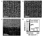
- 6 (a) to 6 (h) are schematic diagrams of a structure of a two-dimensional transition metal dekalconinide grown in various PSR / PMoPs, a cluster-size control mechanism in one embodiment of the present application ((b). And (c)], Raman spectra [(d) and (e)], photoluminescence spectra (f), and XPS spectra [(g) and (h)].
- FIG. 7 is an AFM image of two-dimensional transition metal decalcogenide grown over various substrates over time in various embodiments.
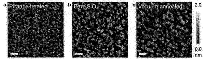
- 8 (a) to 8 (c) are AFM images of two-dimensional transition metal decalcogenides grown on various substrates in one embodiment of the present application.
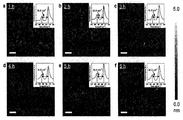
- 9 (a) to 9 (f) are microscopic images of two-dimensional transition metal decalcogenides grown according to various growth times and Raman spectra of the two-dimensional transition metal decalcogenides in one embodiment of the present application. .
- FIG. 10 illustrate, in one embodiment of the present application, an image (a) of a single-layer two-dimensional transition metal decalcogenide grown on a large-area wafer and the two-dimensional transition metal decalcogenide Ellipsometry mapping analysis result (b).
- FIGS. 12A to 12D show a low magnification HRTEM image (a) of a transition metal decalcogenide having a transferred three-dimensional structure in one embodiment of the present application, and any of the two-dimensional transition metal decalcogenides.
- the high magnification of the position of HRTEM is [(b) to (d)].
- FIG. 1 It is a schematic diagram which shows the growth mode of a thin film on the surface of a board
- the thin film is synthesized in the Frank-Van der Merve growth mode due to the high molecular mobility on the substrate surface.
- ML monolayer
- Volmer-Weber growth mode is due to low molecular mobility on the substrate surface.
- Stranski-Krastanow growth mode to synthesize a thin film, the entire substrate can not be covered with a single layer thin film.
- FIG. 15 is a scan showing a result of nucleation at the surface of a substrate according to the concentration of potassium hydroxide solution when the SiO 2 substrate is treated with potassium hydroxide (KOH) solution in the step of reducing the surface energy of the embodiment according to the present invention
- FIG. An electron microscope image.
- FIG. 16 is a scanning electron microscope image showing a result of synthesizing a two-dimensional transition metal decalcogenide thin film with or without using a precursor decomposition promoting catalyst in a deposition step of an embodiment according to the present invention.
- FIG. 17 is a scanning electron microscope image ((a) to (c)) and Raman spectra ((d) and (e)) showing the results of synthesis of a two-dimensional transition metal decalogenide thin film with temperature in a deposition chamber.
- FIG. 18 is a schematic diagram showing the results of synthesis of a two-dimensional transition metal decalcogenide thin film according to the presence or absence of an inhibitor for preventing the generation of a two-dimensional transition metal decalcogenide bilayer in a deposition step of an embodiment according to the present invention. to be.
- Figure 19 is a scanning step showing the results of the synthesis of the two-dimensional transition metal decalcogenide thin film with or without the use of an inhibitor in the deposition step of one embodiment according to the present invention, to prevent the generation of two-dimensional transition metal decalcogenide bilayer An electron microscope image.
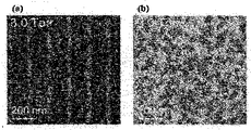
- 20 is a scanning electron microscope image showing a result of synthesizing a two-dimensional transition metal decalcinide thin film according to the pressure in the deposition chamber as an embodiment according to the present invention.
- Figure 21 is an embodiment according to the present invention, the step of generating a nucleus for a predetermined time under the conditions of forming a large number of nuclei on the substrate (a), a small size nucleus generated on the substrate through a pressure change Growing (b) crystals into large sized nucleus crystals; and (c) forming a highly uniform two-dimensional transition metal decalcogenide monolayer thin film on the substrate through a pressure change. It is a schematic diagram which shows the manufacturing method of a metal decalcogenide thin film.
- the term "combination (s) thereof" included in the expression of a makushi form refers to one or more mixtures or combinations selected from the group consisting of components described in the expression of makushi form, It means to include one or more selected from the group consisting of the above components.
- transition metal dichalcogenide particles produced by the gas phase reaction of chalcogen atoms and transition metal atoms produced by the decomposition reaction of chalcogen-containing precursors and transition metal-containing precursors supplied into a deposition chamber are referred to as "clusters.” Is called.
- the chalcogen-containing precursor and the transition metal-containing precursor supplied in the deposition chamber are attached to the surface of the substrate and then generated by the surface reaction of the chalcogen atom and the transition metal atom, or by gas phase reaction. After the resulting clusters have diffused to the surface of the substrate, the transition metal decalcogenide particles produced by the surface reaction are called "crystals".
- a first aspect of the invention includes the steps of pretreating a substrate in a deposition chamber; And supplying a chalcogen-containing precursor and a transition metal-containing precursor in the deposition chamber to deposit a two-dimensional transition metal decalcogenide on the substrate. do.
- the cluster size and nucleation position of the two-dimensional transition metal dekalkozinide by controlling the cluster size and nucleation position of the two-dimensional transition metal dekalkozinide, it is possible to produce a high quality large area two-dimensional transition metal dekalkozinide at a low temperature of about 600 °C or less, The device having excellent electrical performance can be manufactured using the two-dimensional transition metal decalcogenide.
- the deposition may be performed at a low temperature of about 600 ° C or less, but may not be limited thereto.
- the temperature range is about 600 ° C. or less, about 500 ° C. or less, about 400 ° C. or less, about 100 ° C. to about 600 ° C., about 200 ° C. to about 600 ° C., about 400 ° C. to about 600 ° C., about 100 ° C. To about 400 ° C., or about 200 ° C. to about 400 ° C., but may not be limited thereto.
- the deposition may be used without particular limitation deposition methods known in the art, for example, may be performed by chemical vapor deposition, but may not be limited thereto.
- the chemical vapor deposition method is low pressure chemical vapor deposition (LPCVD), atmospheric pressure chemical vapor deposition (APCVD), metal organic chemical vapor deposition (MOCVD) ), Plasma-enhanced chemical vapor deposition (PECVD), inductively coupled plasma-chemical vapor deposition (ICP-CVD), atomic layer deposition, or plasma atomic layer deposition. This may not be limited.
- the transition metal-containing precursor is Ti, V, Cr, Mn, Fe, Co, Ni, Cu, Zn, Nb, Ta, Mo, W, Tc, Re, Ru, Os, Rh It may include a transition metal selected from the group consisting of, Ir, Pt, Ag, Au, Cd, In, Tl, Sn, Pb, Sb, Bi, Zr, Te, Pd, Hf, and combinations thereof However, this may not be limited.
- the transition metal-containing precursor may include one selected from the group consisting of Mo (CO) 6 , Mo (Cl) 5 , MoO (Cl) 4 , MoO 3 , and combinations thereof, This may not be limited.
- the chalcogen-containing precursor is H 2 S, CS 2 , SO 2 , S 2 , H 2 Se, H 2 Te, R 1 SR 2 (Wherein R 1 and R 2 are each independently an alkyl group having 1 to 6 carbon atoms, an alkenyl group having 2 to 6 carbon atoms, or an alkynyl group having 2 to 6 carbon atoms), (NH 4 ) 2 S, C 6 H 8 OS , S (C 6 H 4 NH 2 ) 2 , Na 2 SH 2 O And combinations thereof may be selected, preferably H 2 S, CS 2 , SO 2 , S 2 , R 1 SR 2 (Wherein R 1 and R 2 are each independently an alkyl group having 1 to 6 carbon atoms, an alkenyl group having 2 to 6 carbon atoms, or an alkynyl group having 2 to 6 carbon atoms), (NH 4 ) 2 S, C 6 H 8 OS , S (C 6 H 4 NH 2 ) 2 , Na
- the cluster size of the two-dimensional transition metal decalogenide deposited may be controlled, but may not be limited thereto. As the cluster size is controlled, a structural change of the two-dimensional transition metal decalcogenide deposited may occur, but may not be limited thereto.
- the chalcogen-containing precursor in the deposition process, is supplied into the deposition chamber by adjusting the pressure in the deposition chamber without using a carrier gas or by finely adjusting the flow rate of the carrier gas and
- the partial pressure ratio of the chalcogen-containing precursor to the transition metal-containing precursor may be finely controlled, but may not be limited thereto.
- the partial pressure ratio of the chalcogen-containing precursor to the transition metal-containing precursor is controlled to the size of the cluster formed by the gas phase reaction in the deposition process of the transition metal dichalcogenide and the surface
- the energy may be adjusted to induce two-dimensional growth of the transition metal dichalcogenide, but may not be limited thereto.
- a gas phase reaction and a reaction at the surface of the substrate occur simultaneously, and gaseous substances in the gas phase reaction React to form clusters of transition metal dichalcogenide, which are transferred to the substrate surface to cause a surface reaction.
- the cluster is formed to a larger size at a lower partial pressure ratio (P CP / P MP ) of the chalcogen-containing precursor to the transition metal-containing precursor, and is transferred to the substrate surface, whereby nuclear growth occurs at the substrate surface.
- P CP / P MP partial pressure ratio
- the gaseous matter sticks to the side, it grows in the form of islands (up to a certain size, called the nucleus, and when the size increases, it is called an island).
- clusters generated from the gaseous substance are also transferred to the substrate surface by diffusion.
- the substrate surface temperature is a high temperature condition (for example, a temperature of 550 °C or more)
- the crystal can be grown in a two-dimensional structure by the surface diffusion effect, but the surface temperature of the substrate is a low temperature condition (for example, 500 Temperature below ⁇ ⁇ , this surface diffusion effect does not occur actively because of lack of energy.
- P CP / P MP partial pressure ratio of the chalcogen-containing precursor to the transition metal-containing precursor so as to reduce the cluster size generated by the gas phase reaction, and reducing the surface energy of the substrate during the surface reaction. It is possible to control the structure of the two-dimensional transition metal decalogenide thin film deposited under low temperature conditions.
- the deposited two-dimensional transition metal decalcogenide is two-dimensional in an irregular three-dimensional region. It may be changed to the mixed structure of the triangular region, but may not be limited thereto.
- the higher the partial pressure ratio (P CP / P MP ) of the chalcogen-containing precursor to the transition metal precursor the lower the surface energy of the resulting transition metal decalcogenide and thus the transition. Two-dimensional growth of metal decalcogenide can be induced.
- the two-dimensional transition metal dichalcogenide becomes smaller in crystal size. And can be completely transformed into a two-dimensional triangle region.
- the ratio of the chalcogen-containing precursor partial pressure / transition metal-containing precursor partial pressure may be about 1/2 or more or about 2 or more, but may not be limited thereto.
- the feed partial pressure ratio of the chalcogen-containing precursor to the transition metal-containing precursor may be about 1: about 2 or more, about 1: about 3 or more, about 1: about 4 or more, about 1: about 5 or more, or About 1: about 10 or more, but may not be limited thereto.
- the feed partial pressure ratio of the chalcogen-containing precursor to the transition metal-containing precursor is about 1: about 2 to about 600, about 1: about 2 to about 500, about 1: about 2 to about 400, about 1: About 2 to about 300, about 1: about 2 to about 200, or about 1: about 2 to about 100, but may not be limited thereto.
- a gas phase reaction and a reaction on the surface of the substrate occur, and gaseous substances react with each other in the gas phase reaction to form a cluster, and the cluster is the substrate surface. Is transferred to the surface reaction.
- P CP / P MP partial pressure ratio of the chalcogen-containing precursor to the transition metal-containing precursor
- the partial pressure ratio (P CP / P MP ) of the chalcogen-containing precursor to the transition metal-containing precursor is increased to reduce the cluster size of the transition metal dichalcogenide produced by the gas phase reaction and to reduce the surface of the substrate.
- the energy can be reduced to induce two-dimensional growth of the transition metal decalcogenide.
- the pressure in the deposition chamber is adjusted to adjust the amount of chalcogen-containing precursor and transition metal-containing precursor supplied into the deposition chamber, thereby reducing the partial pressure of chalcogen-containing precursor /
- the ratio of transition metal-containing precursor partial pressure (P CP / P MP ) can be adjusted.
- the chalcogen-containing precursor and the transition metal-containing material are supplied into the deposition chamber by adjusting the pressure in the deposition chamber without using a carrier gas or through fine control of the carrier gas flow rate.
- the ratio (P CP / P MP ) of the partial pressure of the chalcogen-containing precursor / transition metal-containing precursor may be finely controlled, but is not limited thereto.
- volatile by-products are grown by desorption and surface diffusion in the pseudo-2 dimensional region. It can be changed to a single layer by, but may not be limited thereto.
- the partial pressure ratio (P CP / P MP ) of the chalcogen-containing precursor to the transition metal-containing precursor when the partial pressure ratio (P CP / P MP ) of the chalcogen-containing precursor to the transition metal-containing precursor is low, an irregular three-dimensional region having a small grain size may be grown, but It may not be limited.
- transition metal dichalcogenide when transition metal dichalcogenide is grown at a low partial pressure ratio of the chalcogen-containing precursor to the transition metal-containing precursor, a large amount of transition metal-containing precursor vapor and large sized clusters are generated. The clusters thus adsorbed on the substrate surface can grow three-dimensional regions, so that the partial pressure ratio is preferably increased.
- the nucleation position of the two-dimensional transition metal decalcogenide deposited on the substrate may be artificially controlled, but may not be limited thereto.
- the grain size of the two-dimensional transition metal decalcogenide having a limited grain size may be adjusted, but may not be limited thereto.
- the pretreatment of the substrate may include, but is not limited to, a treatment selected from the group consisting of vacuum heat treatment, annealing or high vacuum annealing treatment, chemical treatment, and combinations thereof.
- the pretreatment can be a high vacuum annealing treatment, whereby nucleation sites can be suppressed by degrading dangling bonds that provide reactive surface locations on the substrate by the high vacuum annealing, thus providing high quality
- Large-area two-dimensional transition metal dikalkogenide may be prepared, but may not be limited thereto.
- the substrate is Si, SiO 2 , Ge, GaN, AlN, GaP, InP, GaAs, SiC, Al 2 O 3 , LiAlO 3 , MgO, glass, quartz, sapphire, graphite, graphene , Plastics, polymers, boron nitride (h-BN) and combinations thereof may be selected from the group consisting of, but may not be limited thereto.
- the substrate may be a material that is difficult to synthesize due to problems such as atomic arrangement, or a material that is advantageous in price or large area, and may serve as a substrate for controlling the catalyst or nucleation site for growing the cluster.
- the method before the pretreatment of the substrate, the method may further include pre-cleaning the substrate to prevent unnecessary nucleation near the grain, but is not limited thereto. You may not.
- the pre-cleaning step may be performed under atmospheric conditions, but may not be limited thereto.
- the pre-cleaning may be performed by water, ethanol, acidic substances, alcohols, or RCA cleaning method, but may not be limited thereto.
- the alcohols may include methanol, ethanol, propanol, butanol, or an isomer thereof, but may not be limited thereto.
- the acidic substance may include is selected from the group consisting of H 2 SO 4, HCl, HNO 3, and combinations thereof, but may not be limited thereto.
- the acidic material may be diluted and used in various ratios, but may not be limited thereto.
- the RCA cleaning may be performed using a combination of NH 4 OH, H 2 O 2 , and / or HCl, depending on the combination of ammoniacal SC-1 washing or acidic SC-2. It may be divided into a cleaning method, but may not be limited thereto.
- the grain size of the two-dimensional transition metal dekalkozinide may be about 10 nm or more than about 50 nm, but may not be limited thereto.
- the grain size of the two-dimensional transition metal dekalconzide is about 10 nm or more, about 30 nm or more, about 50 nm or more, about 70 nm or more or about 100 nm or more, about 200 nm or less, about 150 nm or less About 130 nm or less, or about 100 nm or less, specifically about 10 nm to about 200 nm, about 30 nm to about 200 nm, about 50 nm to about 200 nm, about 50 nm to about 100 nm, about 50 nm to About 90 nm, about 50 nm to about 80 nm, about 50 nm to 70 nm, about 50 nm to about 60 nm, about 60 nm to about 100 nm, about 60 nm to about 90
- the two-dimensional transition metal dekalkozinide may be applied to all electronic circuits and electronic devices, but may not be limited thereto.
- it may be possible to manufacture a field effect transistor, an optical sensor, a light emitting device, a photodetector, a magneto-optical memory device, a photocatalyst, a flat panel display, a flexible device, and a solar cell using the device, but is not limited thereto. You may not.
- the field effect transistor including the two-dimensional transition metal decalcogenide is excellent in electrical performance, there is a characteristic that shows the tendency of the conventional n-type semiconductor.
- a second aspect of the present invention includes the steps of reducing the surface energy of a substrate through surface treatment of the substrate in a deposition chamber; And supplying a chalcogen-containing precursor, a transition metal-containing precursor, and a precursor decomposition promoting catalyst in the deposition chamber to deposit a two-dimensional transition metal decalcogenide monolayer on the substrate.
- the present invention relates to a method for producing a transition metal decalcogenide thin film.
- the method for manufacturing a two-dimensional transition metal decalcogenide thin film according to the present invention may include reducing surface energy of a substrate through surface treatment of the substrate in a deposition chamber. Reducing the surface energy of the substrate through surface treatment of the substrate is to enrich the nucleation site on the substrate surface.
- the number of nucleation growth sites on the surface of the substrate is a very important factor for forming highly uniform thin films, in particular single layer thin films.
- By controlling the surface energy of the substrate it is possible to control the number of nucleation growth sites on the surface of the substrate, and the number of such nucleation growth locations affects the crystal size of the two-dimensional transition metal dekalconzide and the uniformity of the thin film.
- the crystal of the transition metal decalcogenide is formed to a large size, but the entire substrate is not covered with the two-dimensional transition metal decalcogenide thin film, and the uniformity of the thin film Is lowered.
- the crystals of the transition metal decalcogenide are formed in a small size, but the entire substrate can be covered with the two-dimensional transition metal decalcogenide thin film, and the uniformity of the thin film is Is improved.
- the number of nucleation growth sites on the surface of this substrate can be controlled through surface treatment of the substrate.
- an oxide-based insulator selected from the group consisting of SiO 2 , Al 2 O 3 , HfO 2 , LiAlO 3 , MgO, and combinations thereof is used as the substrate
- existing hydroxyl groups (-OH bonds) are provided to the nucleus growth site, and the number of hydroxyl groups (-OH bonds) can be controlled through surface treatment of various substrates.
- piranha solution treatment sulfuric acid (H 2 SO 4 ) solution treatment, hydrochloric acid (HCl)
- Wet treatment method selected from the group consisting of solution treatment and alkali metal hydroxide solution treatment; Or surface treatment of the substrate by a dry treatment method selected from the group consisting of O 2 plasma treatment and heat treatment using water vapor.
- alkali metal hydroxide solution include potassium hydroxide solution and sodium hydroxide solution.
- the wet treatment method is not limited to the above, and any solution may be used as long as it is a method capable of lowering the surface energy of the oxide-based insulator substrate.
- the content of solute in the solution is at least 0.0001% by weight, preferably from 0.0001% by weight to weight% at maximum solubility (the maximum solubility is different for each solute in each solution, so The upper limit value may vary), but is not limited thereto, and any ratio may be used.
- the dry treatment method is not limited to the above, and any gas or molecule can be used as long as it can lower the surface energy of the oxide-based insulator substrate.
- a method capable of removing hydroxyl groups (-OH bonds) for example, vacuum heat treatment, annealing treatment, A high vacuum annealing treatment and a treatment selected from the group consisting of combinations thereof may be performed, but are not limited thereto, and any method may be used as long as the hydroxyl group (—OH bond) can be removed.
- a high vacuum annealing treatment is selected as the surface treatment method of an oxide-based insulator substrate, the number of nucleation growth sites is increased by decomposing dangling bonds that provide a reactive surface position on the substrate by the high vacuum annealing. It can be suppressed, thereby increasing the size of the transition metal decalcogenide crystals, but may reduce the uniformity of the two-dimensional transition metal decalcogenide thin film.
- a position at which surface defects exist may be provided as a nuclear growth position, and surface energy control by surface treatment of the substrate It is possible to control the surface defects provided to the nucleus growth position. Also in this case, the surface energy of the substrate can be reduced to enrich the nucleus growth position.
- the surface energy of the substrate is reduced through surface treatment of the substrate, thereby enriching the nucleus growth site and consequently reducing the crystal size of the transition metal decalcogenide.
- the uniformity of the two-dimensional transition metal decalcogenide thin film may be improved.
- FIG. 15 shows nucleation at the surface of the substrate according to the concentration of potassium hydroxide solution when the SiO 2 substrate is treated with potassium hydroxide (KOH) solution in the step of reducing the surface energy of the substrate according to the embodiment of the present invention. Scanning electron microscope image showing results.
- FIG. 15 (a) is a scanning electron microscope showing the result of nucleation on the surface of a substrate by supplying a chalcogen-containing precursor and a transition metal-containing precursor into a deposition chamber without performing a surface treatment of the SiO 2 substrate.
- FIG. 15 (b) shows that the SiO 2 substrate is subjected to surface treatment with 1 wt% potassium hydroxide solution, and then the chalcogen-containing precursor and the transition metal-containing precursor are supplied into the deposition chamber on the surface of the substrate.
- FIG. 15 (c) shows the chalcogen-containing precursor and transition metal-containing in the deposition chamber after surface treatment of the SiO 2 substrate with 10 wt% potassium hydroxide solution. Scanning electron microscope image showing the result of nucleation on the surface of the substrate by supplying the precursor.
- FIGS. 15 (a) to 15 (c) As a result of the comparison of FIGS. 15 (a) to 15 (c), when the surface treatment of the substrate was not performed, surface energy of the substrate was not reduced, and the nucleation growth position was rare, resulting in less nucleation (FIG. 15 (a)), when the surface treatment of the substrate using a potassium hydroxide solution is reduced the surface energy of the substrate, there is abundant nucleation growth position was made a lot of nucleation (Fig. 15 (b) And 15 (c)), in particular, the higher the concentration of the potassium hydroxide solution, the more abundantly the nucleus growth sites are generated, and the more nucleation is achieved.
- the substrate is SiO 2 , Al 2 O 3 , HfO 2 , LiAlO 3 , MgO, Si, Ge, GaN, AlN, GaP, InP, GaAs, SiC, glass, quartz, sapphire, graphite, graphene It may be selected from the group consisting of fins, plastics, polymers, boron nitride (h-BN) and combinations thereof, but is not limited thereto.
- h-BN boron nitride
- the substrate a material that is inexpensive in terms of cost and advantageous to a large area may be preferable, and it may be desirable to be able to control the number of nuclear growth sites through surface energy control.
- a method for producing a two-dimensional transition metal decalcogenide thin film according to the present invention is to supply a chalcogen-containing precursor, a transition metal-containing precursor and a precursor decomposition promoting catalyst in a deposition chamber, thereby providing a two-dimensional transition metal decalcogenide monolayer on the substrate. It may include the step of depositing.
- the deposition step for example, in the chemical vapor deposition step, at the substrate surface which is a gas phase reaction and a heterogeneous reaction, which is a homogeneous reaction
- the reaction occurs at the same time.
- gas phase reaction gaseous reactants react with each other to form clusters of transition metal dichalcogenides, which may be transferred to the substrate surface to cause surface reactions.
- the gaseous reactants can react with each other to form crystals of the transition metal dichalcogenide.
- chalcogen-containing precursor and the transition metal-containing precursor are fed into the deposition chamber, precursor decomposition reactions of the chalcogen-containing precursor and the transition metal-containing precursor occur, and the chalcogen is an intermediate product by decomposition of the precursor.
- Atoms and transition metal atoms form clusters of transition metal dichalcogenides through gas phase reactions, which can be transferred to the substrate surface to cause surface reactions.
- chalcogen-containing precursors and transition metal-containing precursors, or chalcogen atoms and transition metal atoms, which are intermediate products due to their decomposition can cause heterogeneous reactions to form crystals of transition metal dichalcogenides.
- the chalcogen-containing precursor and the transition metal-containing precursor each have a specific precursor decomposition temperature, and the decomposition properties of these precursors can be an important factor in determining the synthesis temperature of the two-dimensional transition metal dichalcogenide thin film.
- the synthesis rate may be reduced by an incomplete reaction.
- a precursor decomposition promoting catalyst may be fed into the deposition chamber along with the chalcogen-containing precursor and the transition metal-containing precursor.
- the precursor decomposition promoting catalyst catalyzes the decomposition of the ligand bound to the chalcogen atom from the chalcogen atom in the chalcogen-containing precursor and / or the decomposition of the ligand bound to the transition metal atom from the transition metal atom in the transition metal-containing precursor.
- the precursor decomposition promoting catalyst may be advantageous in terms of commercialization by promoting the decomposition of these precursors to improve the synthesis rate of the two-dimensional transition metal dichalcogenide thin film even at low temperature conditions (for example, a temperature of 500 °C or less).
- the complete decomposition temperature of molybdenum hexacarbonyl is 250 ° C.
- hydrogen is used as a precursor decomposition promoting catalyst
- the synthesis rate of the two-dimensional transition metal dichalcogenide thin film at 250 ° C. can be increased several times compared with the case without using hydrogen, or the two-dimensional transition metal decalcogenide thin film at a temperature lower than 250 ° C.
- the synthesis rate of can be implemented equally.
- the precursor decomposition promoting catalyst is not limited to a gaseous material such as hydrogen, and promotes the decomposition of ligands bound to chalcogen atoms from chalcogen atoms in chalcogen-containing precursors, and / or transition metals. It can be used without limitation as long as it can promote decomposition of the ligand bound to the transition metal atom from the transition metal atom in the -containing precursor.
- FIG. 16 is a scanning electron microscope image showing a synthesis result of a two-dimensional transition metal decalcogenide thin film according to whether a precursor decomposition promoting catalyst is used in a deposition step of an embodiment according to the present invention.
- FIG. 16 (a) shows the results of the synthesis of the two-dimensional transition metal dichalcogenide thin film when H 2 is supplied as a precursor decomposition promoting catalyst together with the chalcogen-containing precursor and the transition metal-containing precursor in the deposition chamber in the depositing step.
- 16 (b) shows a two-dimensional transition metal when a chalcogen-containing precursor and a transition metal-containing precursor were supplied in a deposition step without supplying a precursor decomposition promoting catalyst in a deposition chamber. It is a scanning electron microscope image showing the synthesis result of the decalcogenide thin film.
- an inhibitor for preventing the generation of the two-dimensional transition metal decalkogenide bilayer may be further supplied.
- transition metal decalcogenide bilayers Under low temperature conditions (eg, temperatures below 500 ° C.), it is easy to produce transition metal decalcogenide bilayers, which are the biggest obstacles to the synthesis of uniform two-dimensional transition metal decalcogenide monolayer thin films. It is a limit point of low temperature synthesis. Since the formation of the bilayer provides an active position, the probability of incorporation of impurities is also increased, and as a result, the quality of the two-dimensional transition metal decalcogenide thin film may be degraded.
- FIG. 17 is a scanning electron microscope image ((a) to (c)) and Raman spectra ((d) and (e)) showing the results of synthesis of the two-dimensional transition metal decalcogenide thin film according to the temperature in the deposition chamber. .
- the chalcogen-containing precursor and the transition metal-containing precursor were deposited in the deposition chamber while the temperature in the deposition chamber was set to 350 ° C, 300 ° C and 250 ° C, respectively.
- the temperature in the deposition chamber was set to 350 ° C, 300 ° C and 250 ° C, respectively.
- the temperature in the deposition chamber was set to 350 ° C, 300 ° C and 250 ° C, respectively.
- the temperature in the deposition chamber was set to 350 ° C, 300 ° C and 250 ° C, respectively.
- the A 1g -E 1 2g value is about 19, which is confirmed to be a monolayer of two-dimensional transition metal dichalcogenide.
- the temperature in the deposition chamber is 250 ° C.
- the A 1g -E 1 2g value is increased to about 22, thereby forming a double layer of two-dimensional transition metal dichalcogenide. .
- the inhibitor is introduced into the deposition chamber together with the chalcogen-containing precursor, the transition metal-containing precursor and the precursor decomposition promoting catalyst to prevent the formation of a bilayer which degrades the quality of the two-dimensional transition metal decalcogenide thin film.
- the chalcogen-containing precursor, the transition metal-containing precursor, and the precursor decomposition promoting catalyst may be first fed into the deposition chamber, and after some time the inhibitor may be fed into the deposition chamber.
- FIG. 18 is a schematic diagram showing the results of synthesis of a two-dimensional transition metal decalcogenide thin film according to the presence or absence of the use of an inhibitor to prevent the formation of the two-dimensional transition metal decalcogenide bilayer in the deposition step of the embodiment according to the present invention. .
- a uniform two-dimensional transition is performed initially.
- a metal dichalcogenide monolayer thin film is formed, but because of the low molecular mobility as the crystal size of the transition metal decalcogenide increases, the transition metal decalcogenide molecule adsorbed by van der Waals forces on the two-dimensional transition metal decalcogenide monolayer Does not move to the lateral position of the crystal and provides a new nucleation growth site on the two-dimensional transition metal decalcogenide monolayer.
- a single layer and a double layer of two-dimensional transition metal dichalcogenide may be simultaneously synthesized, and as a result, a non-uniform two-dimensional transition metal dichalcogenide thin film may be formed.
- the transition metal decalcogenide molecule may form a chemical bond only at the side surface of the two-dimensional transition metal decalcogenide monolayer, and consequently, the two-dimensional transition without generating the two-dimensional transition metal decalcogenide bilayer throughout the substrate. Only metal decalcogenide monolayers can be formed. Therefore, when the inhibitor is supplied with the chalcogen-containing precursor, the transition metal-containing precursor and the precursor decomposition promoting catalyst in the deposition chamber, it is possible to prepare a very uniform two-dimensional transition metal decalcogenide monolayer thin film.
- the material that can be used as an inhibitor for preventing the formation of the two-dimensional transition metal decalcogenide bilayer is not particularly limited, and any material that can be physically adsorbed to the base surface of the two-dimensional transition metal decalcogenide monolayer can be used.
- H 2 O can be used as the inhibitor.
- the inhibitor can meet the following requirements.
- the adsorption energy of the inhibitor is higher at the lateral position of the substrate and the transition metal decalcogenide monolayer than the basal plane of the transition metal decalcogenide monolayer, and the adsorption energy of the chalcogen is at It is higher at the base of the substrate and the transition metal decalcogenide monolayer than the lateral position.
- FIG. 19 is a scanning electron showing a result of synthesizing a two-dimensional transition metal decalcogenide thin film according to whether or not an inhibitor is used to prevent generation of a two-dimensional transition metal decalcogenide bilayer in a deposition step of an embodiment according to the present invention. Microscope image.
- a low temperature condition in the deposition steps for example, a temperature not higher than 500 °C
- chalcogen-containing precursor e. G., S- Containing precursor
- a transition metal-containing precursor eg, Mo-containing precursor
- a precursor decomposition promoting catalyst eg, H 2 gas
- the two-dimensional transition metal decalcogenide monolayer grey portion
- the two-dimensional transition metal decalcogenide bilayer black portion
- the chalcogen-containing precursor e.g. S-containing
- a transition metal-containing precursor e.g, Mo-containing precursor
- precursor decomposition promoting catalyst e.g, H 2 gas
- the present invention comprises the steps of (1) reducing the surface energy of the substrate through the surface treatment of the substrate in the deposition chamber; (2) supplying a chalcogen-containing precursor and a transition metal-containing precursor into the deposition chamber under a temperature of 500 ° C. or lower and a pressure of 0.001 Torr to 760 Torr to crystallize two-dimensional transition metal decalcogenide on the substrate.
- step (3) under pressure increased above the pressure in step (2), supplying a chalcogen-containing precursor and a transition metal-containing precursor into the deposition chamber to increase the crystal size of the two-dimensional transition metal decalcogenide on the substrate; ; And (4) supplying a chalcogen-containing precursor and a transition metal-containing precursor into the deposition chamber under pressure greater than the pressure of step (3) to form a two-dimensional transition metal decalcogenide monolayer on the substrate. It relates to a method for producing a two-dimensional transition metal decalcogenide thin film comprising a.
- the precursor decomposition promoting catalyst may be further supplied into the deposition chamber together with the chalcogen-containing precursor and the transition metal-containing precursor.
- the inhibitor for preventing the generation of the two-dimensional transition metal dichalcogenide bilayer, together with the chalcogen-containing precursor and the transition metal-containing precursor, or the chalcogen-containing precursor may be further fed into the deposition chamber.
- the inhibitor may be fed into the deposition chamber simultaneously with the chalcogen-containing precursor, the transition metal-containing precursor and the precursor decomposition promoting catalyst, or the chalcogen-containing precursor, the transition metal-containing precursor and the precursor decomposition promoting catalyst may be supplied.
- the inhibitor may be fed first into, and after some time the inhibitor may be fed into the deposition chamber.
- steps (2) to (4) may be a specific process of depositing a two-dimensional transition metal decalcogenide monolayer.
- a two-dimensional transition metal decalogenide thin film having a small crystal size is synthesized, but in this case, uniformity can be improved.
- a step of reducing the surface energy of the substrate may be performed through surface treatment of the substrate in the deposition chamber. Reducing the surface energy of the substrate through surface treatment of the substrate is to increase the number of nucleation growth sites on the substrate surface.
- a chalcogen-containing precursor, a transition metal-containing precursor, any precursor decomposition promoting catalyst, and any inhibitor are supplied into the deposition chamber on the substrate.
- a step of producing a crystal of the two-dimensional transition metal decalcogenide may be performed. This allows a small number of nuclei to grow on the surface of the substrate, although the crystal size is small at the beginning of synthesis.
- the chalcogen-containing precursor, the transition metal-containing precursor, any precursor decomposition promoting catalyst and any inhibitor are then supplied into the deposition chamber while the temperature of the crystal forming step remains the same while the pressure is increased.
- the step of increasing the crystal size of the two-dimensional transition metal dekalkozinide on the substrate can be performed.
- the increased pressure condition than the crystal formation step is a synthetic condition in which a nucleus formed from small crystals can grow to a large crystal size, and only a pressure higher than the pressure used in the crystal formation step, in particular, the upper limit of the increase in pressure is It is not limited. This change in pressure condition allows nuclei of small crystal size to be augmented to large crystal sizes.
- the pressure in the deposition chamber when the pressure in the deposition chamber is set to 3 Torr in the crystal generation step, the pressure in the deposition chamber may be set to 9 Torr in the crystal size increasing step, but is not particularly limited thereto.
- 20 is a scanning electron microscope image showing a result of synthesizing a two-dimensional transition metal decalogenide thin film according to the pressure in the deposition chamber.
- the chalcogen-containing precursor and the transition metal-containing precursor are fed into the deposition chamber to provide a two-dimensional transition metal decalcogenide on the substrate.
- the nuclei of (MoS 2 ) were generated, the number of nucleations increased and the crystal size thereof decreased, while as shown in FIG. 20 (b), the chalcogen-
- the containing precursor and the transition metal-containing precursor were fed into the deposition chamber to produce nuclei of the two-dimensional transition metal decalcogenide (MoS 2 ) on the substrate, it was confirmed that the crystal size was increased while the number of nucleation was small. have.
- the chalcogen-containing precursor, the transition metal-containing precursor, any precursor decomposition promoting catalyst and any inhibitor are then introduced into the deposition chamber while the temperature of the crystal size increasing step remains the same while the pressure is increased.
- the increased pressure condition than the crystal size increase step is a synthetic condition in which a nucleus grown to a large crystal size can grow into a uniform two-dimensional transition metal decalcogenide monolayer, and only a pressure higher than the pressure used in the crystal size increase step
- the upper limit of the increase in pressure is not limited. Through such a pressure change, it is possible to prepare a two-dimensional transition metal dicacogenide monolayer thin film having improved uniformity.
- the manufacturing method according to the present invention by adjusting the size of the crystal or cluster of the two-dimensional transition metal dekalkogenide and the number of nucleus growth sites, high quality uniformity improved at low temperature conditions of about 500 °C or less
- a large-area two-dimensional transition metal decalcogenide thin film can be prepared, and a device having excellent electrical performance can be manufactured using the prepared two-dimensional transition metal decalcogenide thin film.
- Mo (CO) 6 99.9%, Sigma Aldrich, CAS number 13939-06-5
- Highly doped ( ⁇ 0.005 ⁇ cm) p-type Si with 300 nm-thick SiO 2 layer was used as the substrate.
- the growth was carried out using only precursors sublimated with H 2 S during the growth time at a constant pressure of 0.5 Torr. After growth the substrate was transferred to a load-lock chamber and cooled for 1 hour using an argon flow of 100 sccm. The post-growth treatment was not performed by any known methods (such as argon and H 2 S annealing at high temperatures). All analyzes and characterizations were performed using the grown samples.
- AFM XE-150, Park Systems
- AFM images were measured using very sharp silicon tips with a radius of curvature of less than 5 nm ( ⁇ 5 nm).
- a soft X-ray ionizer module was applied to prevent static during the measurement. The images were taken over an area of 1 ⁇ m 2 to 2 ⁇ m 2 with a resolution of 512 ⁇ 512 pixels and a measurement rate of 0.5 Hz. The image was adjusted to 750 nm 2 .
- Raman spectroscopic measurements of the two-dimensional transition metal decalcozinide prepared in the above examples were performed using a DXR Raman microscope (Thermo Scientific). A laser with an excitation wavelength of 532 nm, a spot size of 0.7 ⁇ m, and a power of 8 mW was used. The estimated spectral resolution is 0.5 cm - was a 1, the Si peak of 520.8 cm -1 were used for normalization (normalization). Photoluminescence (LabRam ARAMIS, Horiba Jobin Yvon) measurements of the grown samples were performed with a wavelength of 514 nm and a laser power of 10 mW.
- BOE silver buffered oxide etching
- the HAADF-STEM image of the two-dimensional transition metal decalcogenide prepared in the above example is a Tis cubed (Cs-STEM) operating at 300 kV using a milliradian convergence angle of 19.3 and a screen current of 50-100 pA. Photographed using G2 60-300, FEI). The image was smoothed and Fourier filtered to enhance contrast.
- Back-gate FET devices were fabricated by depositing Ti / Au (5/50 nm) electrodes directly on MoS 2 monolayers grown using electron-beam deposition.
- the lift-off process was performed by immersion in dichloromethane (DCM) and IPA and drying with high purity N 2 (99.999%).
- the electrical performance of the device was measured at room temperature under ambient conditions using a four-probe station with a precision semiconductor parameter analyzer (4156A, Hewlett-Packard). The device was not annealed.
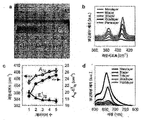
- Vapor pressure and decomposition characteristics of the precursor are important parameters when considering their suitability for CVD processes.
- a home-made measuring system was used. A certain volume of vessel was first maintained under high vacuum conditions by a turbomolecular pump (TMP), then opening the connected quartz tube containing the precursor and until the pressure remained constant It was kept for several hours. Vapor pressures of Mo (CO) 6 at precursor temperatures of 30, 50, and 70 ° C. were measured as 0.31, 1.27, and 5.24 Torr (FIG. 1 (a)), respectively, and a simplified form of the Clapeyron equation, ln (P sat).
- Low temperature growth of stacked MoS 2 a two-dimensional transition metal decalcogenide, was performed using a showerhead-type reactor connected to a gas flow line and a load-lock chamber, as shown in FIGS. 2A and 2B.
- the pre-cleaned or treated (by piranha or high vacuum annealing) SiO 2 substrate was placed into a load-lock chamber and the sample was then transferred to the main chamber.
- the partial pressure of Mo (CO) 6 was precisely controlled using a chiller-heater unit (adjustable range is -20 ° C to 80 ° C).
- the flow rate of H 2 S was controlled using a mass flow controller.
- the use of carrier gases Ar or H 2 has been ruled out to prevent the formation of large size clusters.
- the researchers used a scanning electron microscope (SEM, S-4800, HITACHI), a high resolution transmission electron microscope (HRTEM, Tecnai G2 F30 S-Twin, FEI), and a Raman spectroscopy to identify sulfur-containing precursors.
- SEM scanning electron microscope
- HRTEM high resolution transmission electron microscope
- Tecnai G2 F30 S-Twin, FEI high resolution transmission electron microscope
- Raman spectroscopy Raman spectroscopy
- edge structures can be formed under various conditions. Sulfur coverage according to the edge type produced and related parameters of the S to Mo ratio account for the triangular monolayer domains often found in high quality MoS 2 . Complete, regular, triangular domains exist for S-edge two-dimensional MoS 2 clusters covered with 100% sulfur atoms. Such structures are often formed under high sulfiding conditions.
- the calculated S-to-Mo ratio is expressed as a function of cluster size for various edge types and sulfur coverage.
- the XPS measurement results and AFM images of MoS 2 grown at various P SR / P MoP values indicate that high P SR / P MoP facilitates two-dimensional growth as the surface energy decreases.
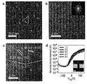
- FIG. 5A and 5B are microscopic images (FIG. 5B) for samples grown at various P SR / P MoP values showing growth window at low temperature (FIG. 5A). Triangular two-dimensional MoS 2 regions were grown under 73 specific P SR / P MoP .
- the scale bar is 200 nm.
- Figure 6 (a) is a different structure from growing in different values of P SR / P MoP of MoS 2 with a (3-D: cases 1 and 2, 3d + 2 D:: case 3, two-dimensional case 4) AFM Image.
- the scale bar is 200 nm.
- the measured height profile of the area is shown in the inset shown by the open yellow square.
- 6 (b) and 6 (c) are schematic diagrams of the cluster-size control mechanism of the present application. The formation of these clusters was limited at higher P SR / P MoP (c), while larger MoS 2 clusters were formed by gas phase reactions at lower P SR / P MoP (b).
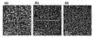
- 8A to 8C are AFM images of MoS 2 monolayer regions grown on different substrates, respectively: (a) piranha-treated MoS 2 , (b) bare MoS 2 , and (c) ) vacuum annealed MoS 2.
- High vacuum annealing de-passivates dangling bonds passivated in untreated SiO 2
- the piranha treatment passivates dangling bonds.
- Large sized islands were grown on high vacuum annealed SiO 2 substrates due to limited nucleation sites.
- the scale bar is 100 nm.
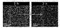
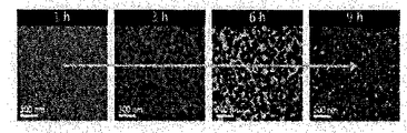
- FIG. 9 (a) shows the initial phase of growth.
- the single-layer small triangular area of MoS 2 was grown at the nucleation position on the SiO 2 substrate.
- FIGS. 9B to 9D the MoS 2 regions were further grown, and polycrystalline monolayer MoS 2 was formed by merging with each other.
- Figures 9 (e) and (f) triangular MoS 2 bilayer regions were grown in fully covered monolayers.
- the corresponding value of ⁇ k in the Raman spectrum for each growth time was measured as 18.8, and 19.3 to 20.3 cm ⁇ 1 for monolayers and monolayers with bilayer regions, respectively.
- FIG. 11D shows photoluminescence of the stacked MoS 2 .
- Two dominant absorption peaks near 670 nm and 620 nm, consistent with two direct excitonic transitions (A1 and B1), were observed and the intensity decreased with increasing number of layers.
- the indirect band gap transition is a multi-layer-was not observed in the deposited sample, which is a typical phenomenon for SiO 2 substrates.
- Figure 10 (a) shows a photograph of a single layer MoS 2 grown on a 4 "SiO 2 / Si wafer. The uniformity of the grown MoS 2 was evaluated by ellipsometry mapping analysis (Fig. 10 (b)). The thickness was 0.7 to 0.8 nm. MoS 2 was successfully grown over the 3 ′′ region. In FIG. 10B, the unit of the insertion value is nanometers.
- FIG. 12A is a low magnification HRTEM image of MoS 2 having a transferred three-dimensional structure (FIG. 1 (a), case 1).
- 12B to 12D show a high magnification image selected at an arbitrary position in FIG. 12A having a corresponding FFT pattern.
- Multi-layered polycrystalline MoS 2 consists of domains of small sized three-dimensional stacked structure, and it is difficult to distinguish grain boundaries due to the interference of overlapping layers and small grain size.
- FIG. 13A is a low magnification STEM-HAADF image of polycrystalline monolayer MoS 2 . A single domain of triangles with an approximate size of 100 nm can be observed and produce grain boundaries (yellow dashed triangles).
- FIG. 13A is a low magnification STEM-HAADF image of polycrystalline monolayer MoS 2 .
- a single domain of triangles with an approximate size of 100 nm can be observed and produce grain boundaries (yellow dashed triangles).
- FIG. 13B is a high magnification STEM-HAADF image of grain boundaries. Two adjacent single crystal domains form a grain boundary with an inclination angle of 31 °. The inset shows an FFT pattern showing the hexagonal structure of the MoS 2 monolayer.
- FIG. 13C is a smoothed and Fourier-filtered image in FIG. 13B. Very uniform and flawless structures were observed for the brighter Mo atoms and the darker S atoms.
- FIG. 13C is a smoothed and Fourier-filtered image in FIG. 13B. Very uniform and flawless structures were observed for the brighter Mo atoms and the darker S atoms.
- 13D is an electrical characteristic of a FET device fabricated to have channel lengths and widths (insertion, scale bar: 5 ⁇ m) of 5 ⁇ m and 10 ⁇ m.
- the mobility of 0.15 cm 2 V ⁇ 1 s ⁇ 1 and the maximum on / off ratio of 10 5 at 5 V were measured at the applied back-gate voltage in the range of ⁇ 150 V to 150 V.
- the monolayer of MoS 2 was not patterned.
- the SiO 2 substrate Prior to growth, the SiO 2 substrate was first pre-cleaned using acetone, isopropyl alcohol (IPA), and deionized water (DI) to prevent nucleation near dust grains. The substrate was then loaded into the load-lock chamber for several seconds under ambient conditions to prevent any surface contamination, then transported to the main reactor, followed by various Mo (CO) 6 sublimation temperatures (0 to 80 ° C.) and H 2 It was grown for a certain time at substrate temperature of 350 ° C. at S flow rate (10-100 sccm). In preliminary experiments conducted at lower P SR / P MoP , structural changes in MoS 2 were observed depending on cluster size, demonstrating that the partial pressure ratio is a major parameter for two-dimensional growth [FIG. a)].
- FIG. 6A shows atomic force microscopy (AFM) photographs of various samples grown at different values of P SR / P MoP .
- AFM atomic force microscopy
- the grain size of the polycrystalline two-dimensional material is the most important property that determines its physical and electrical properties. At low temperatures, the grain size of the two-dimensional material is much smaller than the grain size at high temperatures due to the small diffusion length at the surface.
- We have observed the growth of monocrystalline monolayer MoS 2 domains grown at various values of P SR / P MoP by AFM. However, no grain size greater than 50 nm was observed even under strong sulfiding conditions (P SR / P MoP 594). This experiment indicates the presence of grain-size limitations at 350 ° C. To overcome this limitation due to the short diffusion length on the surface, nucleation sites were artificially manipulated by annealing the substrate at high vacuum.
- Hydroxylated or hydrogen-passivated dangling bonds of amorphous SiO 2 are known to provide many reactive surface sites compared to unsaturated surfaces.
- the high vacuum annealing treatment decomposes the hydrogen-passivated dangling binding entities.
- AFM images obtained at different growth times were obtained at the edges of monolayer regions grown after the MoS 2 nuclei occupied all desired nucleation sites during the initial phase of growth. Attached to the edge and demonstrated that no further nucleation was observed during growth (FIG. 7).
- the monolayer MoS 2 region was grown up to 100 nm on nucleation-position-limited substrates. For the growth of high quality MoS 2 at low temperatures, it is important to control the affinity of the nucleus and the substrate so that the grain-size limitations can be overcome.
- the prepared two-dimensional transition metal cyanide radical Koji the number of MoS 2 layer is pre-controlled in the prior art has been by adjusting the thickness of the deposited Mo, surface energy, or supersaturated.
- the grown MoS 2 using the method of the present invention is characterized by the lamination growth (detailed growth process is shown in Figs. 9A to 9F). Different surface colors were observed in FIG. 11 for different layer numbers, and in FIG. 11 a, a very uniform large area MoS 2 was grown on a 1 ⁇ 1 cm 2 SiO 2 substrate, as confirmed by ellipsometry mapping analysis, It was grown on wafers scaled up to 3 "in size ( Figure 10).
- the inventors also used Raman spectroscopy and photoluminescence to confirm the thickness of the grown MoS 2.
- the Raman spectrum of each sample was As the number of layers increased, the red and blue displacements of E 1 2g and A 1g respectively showed (b) in Fig. 11.
- the ⁇ k values were 18.8, 22.6, 23.6, 24.5, and 25 cm in monolayers to 5 layers, respectively. was determined to be -1. as the corresponding to the two dominant absorption peaks (near 670 nm and 620 nm), the two direct excitonic transitions observed in photoluminescence measurements (each A1 and B1), which in the previous report and To match.
- the original cluster-size control method provides a suitable method for stack growth of MoS 2 at wafer scale.
- FIG. 13A shows a low magnification STEM-HAADF image of a MoS 2 monolayer transferred onto a carbon grid by a conventional wet-etching method.
- White areas represent superimposed MoS 2 monolayers during transfer and gray areas represent polycrystalline MoS 2 monolayers.
- the approximate domain size, indicated by the yellow dashed triangle, is 100 nm, which is consistent with previous observations using AFM (FIG. 9B).
- the high magnification HAADF image of the selected region shows the atomic structure of the grain boundary by two triangular domains (Fig.
- the fast Fourier transform (FFT) pattern in the inset of FIG. 13 (b) shows the hexagonal structure of two single crystal MoS 2 domains having an inclination angle of 31 °. From the image reformed by smoothing and Fourier filtering (FIG. 13 (c)), a uniform single crystal MoS 2 domain was observed and the formation of a polycrystalline MoS 2 monolayer was observed by merging forming grain boundaries. In addition, the samples grown at high P SR / P MoP showed better quality compared to the samples grown at low P SR / P MoP (FIG. 12). This microscopic observation shows that a very uniform and large grain MoS 2 polycrystalline monolayer is grown even at 350 ° C.
- the domain structure and grain boundaries are very similar to MoS 2 grown at higher temperatures.
- the cold grown single layer MoS 2 was used to fabricate the back-gate FET to investigate the electrical performance.
- the device was fabricated using a MoS 2 monolayer without patterning and the channel length and width were 5 and 10 ⁇ m, respectively (inset in FIG. 13 (d)).
- the MoS 2 monolayer was not processed after growth and measurements were obtained at room temperature under ambient conditions.
- the FET device exhibits conventional n-type semiconductor behavior with a mobility of 0.15 cm 2 V ⁇ 1 s ⁇ 1 (FIG. 13 (d)).
- the maximum on / off ratio was 10 5 within a gate voltage range of -150 V to 150 V using a 5 V source-drain bias voltage.
- High-doped ( ⁇ 0.005 ⁇ cm) p-type Si with 300 nm-thick SiO 2 layer was used as the substrate.
- the substrate was pre-cleaned and placed on a silicon carbide (SiC) -coated susceptor in a load-lock chamber in a short time to prevent any contamination in the surrounding environment. Thereafter, surface treatment of the substrate with potassium hydroxide solution was performed to reduce the surface energy of the substrate.
- SiC silicon carbide
- H 2 S as a chalcogen-containing precursor, Mo (CO) 6 ( 99.9%, Sigma Aldrich, CAS number 13939-06-5) as a transition metal-containing precursor, H 2 gas and two-dimensional as a precursor decomposition promoting catalyst MoS 2 thin film, a two-dimensional transition metal decalcogenide thin film, was prepared in a showerhead-type reactor by chemical vapor deposition (CVD) by supplying H 2 O into the chamber as an inhibitor to prevent the formation of a transition metal decalcogenide bilayer. Synthesized. The heating block in the CVD was preheated to 250 ° C. before growth. The susceptor with the substrate was transferred to the reactor and the substrate temperature was increased over 10 minutes in the argon flow.
- CVD chemical vapor deposition
- the synthesis was carried out using only sublimated precursors of H 2 S, Mo (CO) 6 , H 2 and H 2 O during the synthesis time at constant pressure (eg 3.0 Torr). After synthesis the substrate was transferred to a load-lock chamber and cooled for 1 hour using an argon flow of 100 sccm. The treatment after the synthesis was not carried out by any known methods (such as argon and H 2 S annealing at high temperatures).
- the MoS 2 thin film which is a two-dimensional transition metal decalcogenide thin film, was prepared in the same manner as in Example 5 except that H 2 O, which is an inhibitor for preventing the formation of the two-dimensional transition metal decalcogenide bilayer, was not supplied into the chamber. Synthesized.
- High-doped ( ⁇ 0.005 ⁇ cm) p-type Si with 300 nm-thick SiO 2 layer was used as the substrate.
- the substrate was pre-cleaned and placed on a silicon carbide (SiC) -coated susceptor in a load-lock chamber in a short time to prevent any contamination in the surrounding environment. Thereafter, surface treatment of the substrate with potassium hydroxide solution was performed to reduce the surface energy of the substrate.
- SiC silicon carbide
- H 2 S as a chalcogen-containing precursor, Mo (CO) 6 as a transition metal-containing precursor ( 99.9%, Sigma Aldrich, CAS number 13939-06-5), precursor decomposition under constant pressure of 3.0 Torr generating a determination of MoS 2 by the H 2 gas and the two-dimensional transition metal radical Koji arsenide chemical vapor deposition by supplying H 2 O into the chamber (CVD) as an inhibitor for preventing the double-layer generation method on the substrate as a promoting catalyst I was.
- H 2 S, Mo (CO) 6 , H 2 and H 2 O were supplied into the chamber under a constant pressure of 9.0 Torr to increase the crystal size of MoS 2 formed on the substrate.
- H 2 S, Mo (CO) 6 , H 2, and H 2 O were fed into the chamber for a period of time under a constant pressure of more than 9 Torr (eg, 12 Torr).
- a MoS 2 thin film which is a two-dimensional transition metal decalcogenide thin film, was synthesized.
- the heating block in the CVD was preheated to 250 ° C. before growth.
- the susceptor with the substrate was transferred to the reactor and the substrate temperature was increased over 10 minutes in the argon flow.
- After synthesis the substrate was transferred to a load-lock chamber and cooled for 1 hour using an argon flow of 100 sccm.
- the treatment after the synthesis was not carried out by any known methods (such as argon and H 2 S annealing at high temperatures).
Landscapes
- Chemical & Material Sciences (AREA)
- Organic Chemistry (AREA)
- Engineering & Computer Science (AREA)
- Materials Engineering (AREA)
- Metallurgy (AREA)
- General Chemical & Material Sciences (AREA)
- Chemical Kinetics & Catalysis (AREA)
- Mechanical Engineering (AREA)
- Inorganic Chemistry (AREA)
- Crystallography & Structural Chemistry (AREA)
- Chemical Vapour Deposition (AREA)
- Inorganic Compounds Of Heavy Metals (AREA)
Abstract
Priority Applications (2)
| Application Number | Priority Date | Filing Date | Title |
|---|---|---|---|
| JP2017561638A JP6688949B2 (ja) | 2015-07-29 | 2016-07-28 | 2次元遷移金属ジカルコゲナイド薄膜の製造方法 |
| US15/562,545 US10309011B2 (en) | 2015-07-29 | 2016-07-28 | Method for manufacturing two-dimensional transition metal dichalcogemide thin film |
Applications Claiming Priority (4)
| Application Number | Priority Date | Filing Date | Title |
|---|---|---|---|
| KR10-2015-0107443 | 2015-07-29 | ||
| KR1020150107443A KR101770235B1 (ko) | 2015-07-29 | 2015-07-29 | 2 차원 전이금속 디칼코지나이드의 제조 방법 |
| KR1020160093974A KR101881304B1 (ko) | 2016-07-25 | 2016-07-25 | 고균일 2차원 전이금속 디칼코지나이드 박막의 제조 방법 |
| KR10-2016-0093974 | 2016-07-25 |
Publications (1)
| Publication Number | Publication Date |
|---|---|
| WO2017018834A1 true WO2017018834A1 (fr) | 2017-02-02 |
Family
ID=57885387
Family Applications (1)
| Application Number | Title | Priority Date | Filing Date |
|---|---|---|---|
| PCT/KR2016/008303 Ceased WO2017018834A1 (fr) | 2015-07-29 | 2016-07-28 | Procédé de fabrication d'un film mince de dichalcogénure de métal de transition à deux dimensions |
Country Status (3)
| Country | Link |
|---|---|
| US (1) | US10309011B2 (fr) |
| JP (1) | JP6688949B2 (fr) |
| WO (1) | WO2017018834A1 (fr) |
Cited By (7)
| Publication number | Priority date | Publication date | Assignee | Title |
|---|---|---|---|---|
| CN108091699A (zh) * | 2017-12-17 | 2018-05-29 | 华中科技大学 | 基于柔性衬底底栅结构的MoS2TFT器件及制备方法 |
| KR20190040480A (ko) * | 2017-10-10 | 2019-04-18 | 에이에스엠 아이피 홀딩 비.브이. | 주기적 증착에 의해 기판 상에 금속 칼코지나이드를 증착하는 방법 |
| KR20200035338A (ko) * | 2018-09-25 | 2020-04-03 | 타이완 세미콘덕터 매뉴팩쳐링 컴퍼니 리미티드 | 전이 금속 디칼코게나이드를 사용한 전계 효과 트랜지스터 및 그 형성 방법 |
| CN114540958A (zh) * | 2022-02-25 | 2022-05-27 | 南京大学 | 一种双层过渡金属硫族化合物连续薄膜及其制备方法 |
| CN114855266A (zh) * | 2022-03-25 | 2022-08-05 | 南京邮电大学 | 一种二维二硫化钨薄膜晶界的鉴别方法 |
| US20240035199A1 (en) * | 2022-07-27 | 2024-02-01 | Research & Business Foundation Sungkyunkwan University | Single-crystalline stack structure of two-dimensional transition metal chalcogenide and method of fabricating the same |
| CN118598190A (zh) * | 2024-05-25 | 2024-09-06 | 闽都创新实验室 | 一种厚度可控的二维过渡金属氧化物薄膜的制备方法 |
Families Citing this family (389)
| Publication number | Priority date | Publication date | Assignee | Title |
|---|---|---|---|---|
| US10378106B2 (en) | 2008-11-14 | 2019-08-13 | Asm Ip Holding B.V. | Method of forming insulation film by modified PEALD |
| US9394608B2 (en) | 2009-04-06 | 2016-07-19 | Asm America, Inc. | Semiconductor processing reactor and components thereof |
| US8802201B2 (en) | 2009-08-14 | 2014-08-12 | Asm America, Inc. | Systems and methods for thin-film deposition of metal oxides using excited nitrogen-oxygen species |
| US9312155B2 (en) | 2011-06-06 | 2016-04-12 | Asm Japan K.K. | High-throughput semiconductor-processing apparatus equipped with multiple dual-chamber modules |
| US10364496B2 (en) | 2011-06-27 | 2019-07-30 | Asm Ip Holding B.V. | Dual section module having shared and unshared mass flow controllers |
| US10854498B2 (en) | 2011-07-15 | 2020-12-01 | Asm Ip Holding B.V. | Wafer-supporting device and method for producing same |
| US20130023129A1 (en) | 2011-07-20 | 2013-01-24 | Asm America, Inc. | Pressure transmitter for a semiconductor processing environment |
| US9017481B1 (en) | 2011-10-28 | 2015-04-28 | Asm America, Inc. | Process feed management for semiconductor substrate processing |
| US9659799B2 (en) | 2012-08-28 | 2017-05-23 | Asm Ip Holding B.V. | Systems and methods for dynamic semiconductor process scheduling |
| US10714315B2 (en) | 2012-10-12 | 2020-07-14 | Asm Ip Holdings B.V. | Semiconductor reaction chamber showerhead |
| US20160376700A1 (en) | 2013-02-01 | 2016-12-29 | Asm Ip Holding B.V. | System for treatment of deposition reactor |
| US9589770B2 (en) | 2013-03-08 | 2017-03-07 | Asm Ip Holding B.V. | Method and systems for in-situ formation of intermediate reactive species |
| US9484191B2 (en) | 2013-03-08 | 2016-11-01 | Asm Ip Holding B.V. | Pulsed remote plasma method and system |
| US9240412B2 (en) | 2013-09-27 | 2016-01-19 | Asm Ip Holding B.V. | Semiconductor structure and device and methods of forming same using selective epitaxial process |
| US10683571B2 (en) | 2014-02-25 | 2020-06-16 | Asm Ip Holding B.V. | Gas supply manifold and method of supplying gases to chamber using same |
| US10167557B2 (en) | 2014-03-18 | 2019-01-01 | Asm Ip Holding B.V. | Gas distribution system, reactor including the system, and methods of using the same |
| US11015245B2 (en) | 2014-03-19 | 2021-05-25 | Asm Ip Holding B.V. | Gas-phase reactor and system having exhaust plenum and components thereof |
| US10858737B2 (en) | 2014-07-28 | 2020-12-08 | Asm Ip Holding B.V. | Showerhead assembly and components thereof |
| US9890456B2 (en) | 2014-08-21 | 2018-02-13 | Asm Ip Holding B.V. | Method and system for in situ formation of gas-phase compounds |
| US9657845B2 (en) | 2014-10-07 | 2017-05-23 | Asm Ip Holding B.V. | Variable conductance gas distribution apparatus and method |
| US10941490B2 (en) | 2014-10-07 | 2021-03-09 | Asm Ip Holding B.V. | Multiple temperature range susceptor, assembly, reactor and system including the susceptor, and methods of using the same |
| KR102263121B1 (ko) | 2014-12-22 | 2021-06-09 | 에이에스엠 아이피 홀딩 비.브이. | 반도체 소자 및 그 제조 방법 |
| US10529542B2 (en) | 2015-03-11 | 2020-01-07 | Asm Ip Holdings B.V. | Cross-flow reactor and method |
| US10276355B2 (en) | 2015-03-12 | 2019-04-30 | Asm Ip Holding B.V. | Multi-zone reactor, system including the reactor, and method of using the same |
| US10458018B2 (en) | 2015-06-26 | 2019-10-29 | Asm Ip Holding B.V. | Structures including metal carbide material, devices including the structures, and methods of forming same |
| US10600673B2 (en) | 2015-07-07 | 2020-03-24 | Asm Ip Holding B.V. | Magnetic susceptor to baseplate seal |
| US9960072B2 (en) | 2015-09-29 | 2018-05-01 | Asm Ip Holding B.V. | Variable adjustment for precise matching of multiple chamber cavity housings |
| US10211308B2 (en) | 2015-10-21 | 2019-02-19 | Asm Ip Holding B.V. | NbMC layers |
| US10322384B2 (en) | 2015-11-09 | 2019-06-18 | Asm Ip Holding B.V. | Counter flow mixer for process chamber |
| US11139308B2 (en) | 2015-12-29 | 2021-10-05 | Asm Ip Holding B.V. | Atomic layer deposition of III-V compounds to form V-NAND devices |
| US10468251B2 (en) | 2016-02-19 | 2019-11-05 | Asm Ip Holding B.V. | Method for forming spacers using silicon nitride film for spacer-defined multiple patterning |
| US10529554B2 (en) | 2016-02-19 | 2020-01-07 | Asm Ip Holding B.V. | Method for forming silicon nitride film selectively on sidewalls or flat surfaces of trenches |
| US10501866B2 (en) | 2016-03-09 | 2019-12-10 | Asm Ip Holding B.V. | Gas distribution apparatus for improved film uniformity in an epitaxial system |
| US10343920B2 (en) | 2016-03-18 | 2019-07-09 | Asm Ip Holding B.V. | Aligned carbon nanotubes |
| US9892913B2 (en) | 2016-03-24 | 2018-02-13 | Asm Ip Holding B.V. | Radial and thickness control via biased multi-port injection settings |
| US10190213B2 (en) | 2016-04-21 | 2019-01-29 | Asm Ip Holding B.V. | Deposition of metal borides |
| US10865475B2 (en) | 2016-04-21 | 2020-12-15 | Asm Ip Holding B.V. | Deposition of metal borides and silicides |
| US10367080B2 (en) | 2016-05-02 | 2019-07-30 | Asm Ip Holding B.V. | Method of forming a germanium oxynitride film |
| US10032628B2 (en) | 2016-05-02 | 2018-07-24 | Asm Ip Holding B.V. | Source/drain performance through conformal solid state doping |
| KR102592471B1 (ko) | 2016-05-17 | 2023-10-20 | 에이에스엠 아이피 홀딩 비.브이. | 금속 배선 형성 방법 및 이를 이용한 반도체 장치의 제조 방법 |
| US11453943B2 (en) | 2016-05-25 | 2022-09-27 | Asm Ip Holding B.V. | Method for forming carbon-containing silicon/metal oxide or nitride film by ALD using silicon precursor and hydrocarbon precursor |
| US10388509B2 (en) | 2016-06-28 | 2019-08-20 | Asm Ip Holding B.V. | Formation of epitaxial layers via dislocation filtering |
| US10612137B2 (en) | 2016-07-08 | 2020-04-07 | Asm Ip Holdings B.V. | Organic reactants for atomic layer deposition |
| US9859151B1 (en) | 2016-07-08 | 2018-01-02 | Asm Ip Holding B.V. | Selective film deposition method to form air gaps |
| US10714385B2 (en) | 2016-07-19 | 2020-07-14 | Asm Ip Holding B.V. | Selective deposition of tungsten |
| KR102354490B1 (ko) | 2016-07-27 | 2022-01-21 | 에이에스엠 아이피 홀딩 비.브이. | 기판 처리 방법 |
| KR102532607B1 (ko) | 2016-07-28 | 2023-05-15 | 에이에스엠 아이피 홀딩 비.브이. | 기판 가공 장치 및 그 동작 방법 |
| US9887082B1 (en) | 2016-07-28 | 2018-02-06 | Asm Ip Holding B.V. | Method and apparatus for filling a gap |
| US9812320B1 (en) | 2016-07-28 | 2017-11-07 | Asm Ip Holding B.V. | Method and apparatus for filling a gap |
| US10395919B2 (en) | 2016-07-28 | 2019-08-27 | Asm Ip Holding B.V. | Method and apparatus for filling a gap |
| KR102613349B1 (ko) | 2016-08-25 | 2023-12-14 | 에이에스엠 아이피 홀딩 비.브이. | 배기 장치 및 이를 이용한 기판 가공 장치와 박막 제조 방법 |
| US10410943B2 (en) | 2016-10-13 | 2019-09-10 | Asm Ip Holding B.V. | Method for passivating a surface of a semiconductor and related systems |
| US10643826B2 (en) | 2016-10-26 | 2020-05-05 | Asm Ip Holdings B.V. | Methods for thermally calibrating reaction chambers |
| US11532757B2 (en) | 2016-10-27 | 2022-12-20 | Asm Ip Holding B.V. | Deposition of charge trapping layers |
| US10714350B2 (en) | 2016-11-01 | 2020-07-14 | ASM IP Holdings, B.V. | Methods for forming a transition metal niobium nitride film on a substrate by atomic layer deposition and related semiconductor device structures |
| US10643904B2 (en) | 2016-11-01 | 2020-05-05 | Asm Ip Holdings B.V. | Methods for forming a semiconductor device and related semiconductor device structures |
| US10229833B2 (en) | 2016-11-01 | 2019-03-12 | Asm Ip Holding B.V. | Methods for forming a transition metal nitride film on a substrate by atomic layer deposition and related semiconductor device structures |
| US10435790B2 (en) | 2016-11-01 | 2019-10-08 | Asm Ip Holding B.V. | Method of subatmospheric plasma-enhanced ALD using capacitively coupled electrodes with narrow gap |
| US10134757B2 (en) | 2016-11-07 | 2018-11-20 | Asm Ip Holding B.V. | Method of processing a substrate and a device manufactured by using the method |
| KR102546317B1 (ko) | 2016-11-15 | 2023-06-21 | 에이에스엠 아이피 홀딩 비.브이. | 기체 공급 유닛 및 이를 포함하는 기판 처리 장치 |
| US10340135B2 (en) | 2016-11-28 | 2019-07-02 | Asm Ip Holding B.V. | Method of topologically restricted plasma-enhanced cyclic deposition of silicon or metal nitride |
| KR102762543B1 (ko) | 2016-12-14 | 2025-02-05 | 에이에스엠 아이피 홀딩 비.브이. | 기판 처리 장치 |
| US11447861B2 (en) | 2016-12-15 | 2022-09-20 | Asm Ip Holding B.V. | Sequential infiltration synthesis apparatus and a method of forming a patterned structure |
| US11581186B2 (en) | 2016-12-15 | 2023-02-14 | Asm Ip Holding B.V. | Sequential infiltration synthesis apparatus |
| KR102700194B1 (ko) | 2016-12-19 | 2024-08-28 | 에이에스엠 아이피 홀딩 비.브이. | 기판 처리 장치 |
| US10269558B2 (en) | 2016-12-22 | 2019-04-23 | Asm Ip Holding B.V. | Method of forming a structure on a substrate |
| US10867788B2 (en) | 2016-12-28 | 2020-12-15 | Asm Ip Holding B.V. | Method of forming a structure on a substrate |
| US11390950B2 (en) | 2017-01-10 | 2022-07-19 | Asm Ip Holding B.V. | Reactor system and method to reduce residue buildup during a film deposition process |
| US10655221B2 (en) | 2017-02-09 | 2020-05-19 | Asm Ip Holding B.V. | Method for depositing oxide film by thermal ALD and PEALD |
| US10468261B2 (en) | 2017-02-15 | 2019-11-05 | Asm Ip Holding B.V. | Methods for forming a metallic film on a substrate by cyclical deposition and related semiconductor device structures |
| US10283353B2 (en) | 2017-03-29 | 2019-05-07 | Asm Ip Holding B.V. | Method of reforming insulating film deposited on substrate with recess pattern |
| US10529563B2 (en) | 2017-03-29 | 2020-01-07 | Asm Ip Holdings B.V. | Method for forming doped metal oxide films on a substrate by cyclical deposition and related semiconductor device structures |
| KR102457289B1 (ko) | 2017-04-25 | 2022-10-21 | 에이에스엠 아이피 홀딩 비.브이. | 박막 증착 방법 및 반도체 장치의 제조 방법 |
| US10770286B2 (en) | 2017-05-08 | 2020-09-08 | Asm Ip Holdings B.V. | Methods for selectively forming a silicon nitride film on a substrate and related semiconductor device structures |
| US10446393B2 (en) | 2017-05-08 | 2019-10-15 | Asm Ip Holding B.V. | Methods for forming silicon-containing epitaxial layers and related semiconductor device structures |
| US10892156B2 (en) | 2017-05-08 | 2021-01-12 | Asm Ip Holding B.V. | Methods for forming a silicon nitride film on a substrate and related semiconductor device structures |
| US10504742B2 (en) | 2017-05-31 | 2019-12-10 | Asm Ip Holding B.V. | Method of atomic layer etching using hydrogen plasma |
| US10886123B2 (en) | 2017-06-02 | 2021-01-05 | Asm Ip Holding B.V. | Methods for forming low temperature semiconductor layers and related semiconductor device structures |
| US12040200B2 (en) | 2017-06-20 | 2024-07-16 | Asm Ip Holding B.V. | Semiconductor processing apparatus and methods for calibrating a semiconductor processing apparatus |
| US11306395B2 (en) | 2017-06-28 | 2022-04-19 | Asm Ip Holding B.V. | Methods for depositing a transition metal nitride film on a substrate by atomic layer deposition and related deposition apparatus |
| US10685834B2 (en) | 2017-07-05 | 2020-06-16 | Asm Ip Holdings B.V. | Methods for forming a silicon germanium tin layer and related semiconductor device structures |
| KR20190009245A (ko) | 2017-07-18 | 2019-01-28 | 에이에스엠 아이피 홀딩 비.브이. | 반도체 소자 구조물 형성 방법 및 관련된 반도체 소자 구조물 |
| US11018002B2 (en) | 2017-07-19 | 2021-05-25 | Asm Ip Holding B.V. | Method for selectively depositing a Group IV semiconductor and related semiconductor device structures |
| US10541333B2 (en) | 2017-07-19 | 2020-01-21 | Asm Ip Holding B.V. | Method for depositing a group IV semiconductor and related semiconductor device structures |
| US11374112B2 (en) | 2017-07-19 | 2022-06-28 | Asm Ip Holding B.V. | Method for depositing a group IV semiconductor and related semiconductor device structures |
| US10605530B2 (en) | 2017-07-26 | 2020-03-31 | Asm Ip Holding B.V. | Assembly of a liner and a flange for a vertical furnace as well as the liner and the vertical furnace |
| US10312055B2 (en) | 2017-07-26 | 2019-06-04 | Asm Ip Holding B.V. | Method of depositing film by PEALD using negative bias |
| US10590535B2 (en) | 2017-07-26 | 2020-03-17 | Asm Ip Holdings B.V. | Chemical treatment, deposition and/or infiltration apparatus and method for using the same |
| TWI815813B (zh) | 2017-08-04 | 2023-09-21 | 荷蘭商Asm智慧財產控股公司 | 用於分配反應腔內氣體的噴頭總成 |
| US10692741B2 (en) | 2017-08-08 | 2020-06-23 | Asm Ip Holdings B.V. | Radiation shield |
| US10770336B2 (en) | 2017-08-08 | 2020-09-08 | Asm Ip Holding B.V. | Substrate lift mechanism and reactor including same |
| US11769682B2 (en) | 2017-08-09 | 2023-09-26 | Asm Ip Holding B.V. | Storage apparatus for storing cassettes for substrates and processing apparatus equipped therewith |
| US10249524B2 (en) | 2017-08-09 | 2019-04-02 | Asm Ip Holding B.V. | Cassette holder assembly for a substrate cassette and holding member for use in such assembly |
| US11139191B2 (en) | 2017-08-09 | 2021-10-05 | Asm Ip Holding B.V. | Storage apparatus for storing cassettes for substrates and processing apparatus equipped therewith |
| USD900036S1 (en) | 2017-08-24 | 2020-10-27 | Asm Ip Holding B.V. | Heater electrical connector and adapter |
| US11830730B2 (en) | 2017-08-29 | 2023-11-28 | Asm Ip Holding B.V. | Layer forming method and apparatus |
| US11295980B2 (en) | 2017-08-30 | 2022-04-05 | Asm Ip Holding B.V. | Methods for depositing a molybdenum metal film over a dielectric surface of a substrate by a cyclical deposition process and related semiconductor device structures |
| US11056344B2 (en) | 2017-08-30 | 2021-07-06 | Asm Ip Holding B.V. | Layer forming method |
| KR102491945B1 (ko) | 2017-08-30 | 2023-01-26 | 에이에스엠 아이피 홀딩 비.브이. | 기판 처리 장치 |
| KR102401446B1 (ko) | 2017-08-31 | 2022-05-24 | 에이에스엠 아이피 홀딩 비.브이. | 기판 처리 장치 |
| US10607895B2 (en) | 2017-09-18 | 2020-03-31 | Asm Ip Holdings B.V. | Method for forming a semiconductor device structure comprising a gate fill metal |
| KR102630301B1 (ko) | 2017-09-21 | 2024-01-29 | 에이에스엠 아이피 홀딩 비.브이. | 침투성 재료의 순차 침투 합성 방법 처리 및 이를 이용하여 형성된 구조물 및 장치 |
| US10844484B2 (en) | 2017-09-22 | 2020-11-24 | Asm Ip Holding B.V. | Apparatus for dispensing a vapor phase reactant to a reaction chamber and related methods |
| US10658205B2 (en) | 2017-09-28 | 2020-05-19 | Asm Ip Holdings B.V. | Chemical dispensing apparatus and methods for dispensing a chemical to a reaction chamber |
| US10403504B2 (en) | 2017-10-05 | 2019-09-03 | Asm Ip Holding B.V. | Method for selectively depositing a metallic film on a substrate |
| US10923344B2 (en) | 2017-10-30 | 2021-02-16 | Asm Ip Holding B.V. | Methods for forming a semiconductor structure and related semiconductor structures |
| US10910262B2 (en) | 2017-11-16 | 2021-02-02 | Asm Ip Holding B.V. | Method of selectively depositing a capping layer structure on a semiconductor device structure |
| KR102443047B1 (ko) | 2017-11-16 | 2022-09-14 | 에이에스엠 아이피 홀딩 비.브이. | 기판 처리 장치 방법 및 그에 의해 제조된 장치 |
| US11022879B2 (en) | 2017-11-24 | 2021-06-01 | Asm Ip Holding B.V. | Method of forming an enhanced unexposed photoresist layer |
| CN111316417B (zh) | 2017-11-27 | 2023-12-22 | 阿斯莫Ip控股公司 | 与批式炉偕同使用的用于储存晶圆匣的储存装置 |
| KR102633318B1 (ko) | 2017-11-27 | 2024-02-05 | 에이에스엠 아이피 홀딩 비.브이. | 청정 소형 구역을 포함한 장치 |
| US10290508B1 (en) | 2017-12-05 | 2019-05-14 | Asm Ip Holding B.V. | Method for forming vertical spacers for spacer-defined patterning |
| KR102184699B1 (ko) | 2017-12-13 | 2020-12-01 | 한양대학교 에리카산학협력단 | 전이금속-디칼코게나이드 박막, 및 그 제조 방법 |
| US10872771B2 (en) | 2018-01-16 | 2020-12-22 | Asm Ip Holding B. V. | Method for depositing a material film on a substrate within a reaction chamber by a cyclical deposition process and related device structures |
| TWI799494B (zh) | 2018-01-19 | 2023-04-21 | 荷蘭商Asm 智慧財產控股公司 | 沈積方法 |
| KR102695659B1 (ko) | 2018-01-19 | 2024-08-14 | 에이에스엠 아이피 홀딩 비.브이. | 플라즈마 보조 증착에 의해 갭 충진 층을 증착하는 방법 |
| USD903477S1 (en) | 2018-01-24 | 2020-12-01 | Asm Ip Holdings B.V. | Metal clamp |
| US11018047B2 (en) | 2018-01-25 | 2021-05-25 | Asm Ip Holding B.V. | Hybrid lift pin |
| USD880437S1 (en) | 2018-02-01 | 2020-04-07 | Asm Ip Holding B.V. | Gas supply plate for semiconductor manufacturing apparatus |
| US10535516B2 (en) | 2018-02-01 | 2020-01-14 | Asm Ip Holdings B.V. | Method for depositing a semiconductor structure on a surface of a substrate and related semiconductor structures |
| US11081345B2 (en) | 2018-02-06 | 2021-08-03 | Asm Ip Holding B.V. | Method of post-deposition treatment for silicon oxide film |
| US11685991B2 (en) | 2018-02-14 | 2023-06-27 | Asm Ip Holding B.V. | Method for depositing a ruthenium-containing film on a substrate by a cyclical deposition process |
| US10896820B2 (en) | 2018-02-14 | 2021-01-19 | Asm Ip Holding B.V. | Method for depositing a ruthenium-containing film on a substrate by a cyclical deposition process |
| US10731249B2 (en) | 2018-02-15 | 2020-08-04 | Asm Ip Holding B.V. | Method of forming a transition metal containing film on a substrate by a cyclical deposition process, a method for supplying a transition metal halide compound to a reaction chamber, and related vapor deposition apparatus |
| KR102636427B1 (ko) | 2018-02-20 | 2024-02-13 | 에이에스엠 아이피 홀딩 비.브이. | 기판 처리 방법 및 장치 |
| US10658181B2 (en) | 2018-02-20 | 2020-05-19 | Asm Ip Holding B.V. | Method of spacer-defined direct patterning in semiconductor fabrication |
| US10975470B2 (en) | 2018-02-23 | 2021-04-13 | Asm Ip Holding B.V. | Apparatus for detecting or monitoring for a chemical precursor in a high temperature environment |
| US11473195B2 (en) | 2018-03-01 | 2022-10-18 | Asm Ip Holding B.V. | Semiconductor processing apparatus and a method for processing a substrate |
| US11447862B2 (en) | 2018-03-07 | 2022-09-20 | Uchicago Argonne, Llc | Methods to deposit controlled thin layers of transition metal dichalcogenides |
| US11393681B2 (en) | 2018-03-07 | 2022-07-19 | Uchicago Argonne, Llc | Methods to deposit and etch controlled thin layers of transition metal dichalcogenides |
| US11629406B2 (en) | 2018-03-09 | 2023-04-18 | Asm Ip Holding B.V. | Semiconductor processing apparatus comprising one or more pyrometers for measuring a temperature of a substrate during transfer of the substrate |
| US11114283B2 (en) | 2018-03-16 | 2021-09-07 | Asm Ip Holding B.V. | Reactor, system including the reactor, and methods of manufacturing and using same |
| KR102646467B1 (ko) | 2018-03-27 | 2024-03-11 | 에이에스엠 아이피 홀딩 비.브이. | 기판 상에 전극을 형성하는 방법 및 전극을 포함하는 반도체 소자 구조 |
| US10510536B2 (en) | 2018-03-29 | 2019-12-17 | Asm Ip Holding B.V. | Method of depositing a co-doped polysilicon film on a surface of a substrate within a reaction chamber |
| US11088002B2 (en) | 2018-03-29 | 2021-08-10 | Asm Ip Holding B.V. | Substrate rack and a substrate processing system and method |
| US11230766B2 (en) | 2018-03-29 | 2022-01-25 | Asm Ip Holding B.V. | Substrate processing apparatus and method |
| KR102501472B1 (ko) | 2018-03-30 | 2023-02-20 | 에이에스엠 아이피 홀딩 비.브이. | 기판 처리 방법 |
| KR102600229B1 (ko) | 2018-04-09 | 2023-11-10 | 에이에스엠 아이피 홀딩 비.브이. | 기판 지지 장치, 이를 포함하는 기판 처리 장치 및 기판 처리 방법 |
| DE102018109936A1 (de) * | 2018-04-25 | 2019-10-31 | Aixtron Se | Mit mehreren zweidimensionalen Schichten beschichtetes Bauteil sowie Beschichtungsverfahren |
| KR102709511B1 (ko) | 2018-05-08 | 2024-09-24 | 에이에스엠 아이피 홀딩 비.브이. | 기판 상에 산화물 막을 주기적 증착 공정에 의해 증착하기 위한 방법 및 관련 소자 구조 |
| US12025484B2 (en) | 2018-05-08 | 2024-07-02 | Asm Ip Holding B.V. | Thin film forming method |
| US12272527B2 (en) | 2018-05-09 | 2025-04-08 | Asm Ip Holding B.V. | Apparatus for use with hydrogen radicals and method of using same |
| KR20190129718A (ko) | 2018-05-11 | 2019-11-20 | 에이에스엠 아이피 홀딩 비.브이. | 기판 상에 피도핑 금속 탄화물 막을 형성하는 방법 및 관련 반도체 소자 구조 |
| KR102596988B1 (ko) | 2018-05-28 | 2023-10-31 | 에이에스엠 아이피 홀딩 비.브이. | 기판 처리 방법 및 그에 의해 제조된 장치 |
| US11718913B2 (en) | 2018-06-04 | 2023-08-08 | Asm Ip Holding B.V. | Gas distribution system and reactor system including same |
| TWI840362B (zh) | 2018-06-04 | 2024-05-01 | 荷蘭商Asm Ip私人控股有限公司 | 水氣降低的晶圓處置腔室 |
| US11286562B2 (en) | 2018-06-08 | 2022-03-29 | Asm Ip Holding B.V. | Gas-phase chemical reactor and method of using same |
| US10797133B2 (en) | 2018-06-21 | 2020-10-06 | Asm Ip Holding B.V. | Method for depositing a phosphorus doped silicon arsenide film and related semiconductor device structures |
| KR102568797B1 (ko) | 2018-06-21 | 2023-08-21 | 에이에스엠 아이피 홀딩 비.브이. | 기판 처리 시스템 |
| US11492703B2 (en) | 2018-06-27 | 2022-11-08 | Asm Ip Holding B.V. | Cyclic deposition methods for forming metal-containing material and films and structures including the metal-containing material |
| CN120591748A (zh) | 2018-06-27 | 2025-09-05 | Asm Ip私人控股有限公司 | 用于形成含金属的材料的循环沉积方法及膜和结构 |
| KR102686758B1 (ko) | 2018-06-29 | 2024-07-18 | 에이에스엠 아이피 홀딩 비.브이. | 박막 증착 방법 및 반도체 장치의 제조 방법 |
| US10612136B2 (en) | 2018-06-29 | 2020-04-07 | ASM IP Holding, B.V. | Temperature-controlled flange and reactor system including same |
| US10388513B1 (en) | 2018-07-03 | 2019-08-20 | Asm Ip Holding B.V. | Method for depositing silicon-free carbon-containing film as gap-fill layer by pulse plasma-assisted deposition |
| US10755922B2 (en) | 2018-07-03 | 2020-08-25 | Asm Ip Holding B.V. | Method for depositing silicon-free carbon-containing film as gap-fill layer by pulse plasma-assisted deposition |
| US10767789B2 (en) | 2018-07-16 | 2020-09-08 | Asm Ip Holding B.V. | Diaphragm valves, valve components, and methods for forming valve components |
| CN109136870B (zh) * | 2018-07-19 | 2020-12-01 | 吴江南玻华东工程玻璃有限公司 | 过渡态氧化镍铬膜层的制备方法及包含该过渡态氧化镍铬膜层的可钢化低辐射镀膜玻璃 |
| US10483099B1 (en) | 2018-07-26 | 2019-11-19 | Asm Ip Holding B.V. | Method for forming thermally stable organosilicon polymer film |
| US11053591B2 (en) | 2018-08-06 | 2021-07-06 | Asm Ip Holding B.V. | Multi-port gas injection system and reactor system including same |
| US10883175B2 (en) | 2018-08-09 | 2021-01-05 | Asm Ip Holding B.V. | Vertical furnace for processing substrates and a liner for use therein |
| US10829852B2 (en) | 2018-08-16 | 2020-11-10 | Asm Ip Holding B.V. | Gas distribution device for a wafer processing apparatus |
| US11430674B2 (en) | 2018-08-22 | 2022-08-30 | Asm Ip Holding B.V. | Sensor array, apparatus for dispensing a vapor phase reactant to a reaction chamber and related methods |
| DE102018120580A1 (de) * | 2018-08-23 | 2020-02-27 | Infineon Technologies Ag | Vorrichtung und verfahren zum abscheiden einer schicht bei atmosphärendruck |
| US11024523B2 (en) | 2018-09-11 | 2021-06-01 | Asm Ip Holding B.V. | Substrate processing apparatus and method |
| KR102707956B1 (ko) | 2018-09-11 | 2024-09-19 | 에이에스엠 아이피 홀딩 비.브이. | 박막 증착 방법 |
| US11049751B2 (en) | 2018-09-14 | 2021-06-29 | Asm Ip Holding B.V. | Cassette supply system to store and handle cassettes and processing apparatus equipped therewith |
| CN110970344B (zh) | 2018-10-01 | 2024-10-25 | Asmip控股有限公司 | 衬底保持设备、包含所述设备的系统及其使用方法 |
| US11232963B2 (en) | 2018-10-03 | 2022-01-25 | Asm Ip Holding B.V. | Substrate processing apparatus and method |
| KR102592699B1 (ko) | 2018-10-08 | 2023-10-23 | 에이에스엠 아이피 홀딩 비.브이. | 기판 지지 유닛 및 이를 포함하는 박막 증착 장치와 기판 처리 장치 |
| US10847365B2 (en) | 2018-10-11 | 2020-11-24 | Asm Ip Holding B.V. | Method of forming conformal silicon carbide film by cyclic CVD |
| US10811256B2 (en) | 2018-10-16 | 2020-10-20 | Asm Ip Holding B.V. | Method for etching a carbon-containing feature |
| KR102605121B1 (ko) | 2018-10-19 | 2023-11-23 | 에이에스엠 아이피 홀딩 비.브이. | 기판 처리 장치 및 기판 처리 방법 |
| KR102546322B1 (ko) | 2018-10-19 | 2023-06-21 | 에이에스엠 아이피 홀딩 비.브이. | 기판 처리 장치 및 기판 처리 방법 |
| USD948463S1 (en) | 2018-10-24 | 2022-04-12 | Asm Ip Holding B.V. | Susceptor for semiconductor substrate supporting apparatus |
| US10381219B1 (en) | 2018-10-25 | 2019-08-13 | Asm Ip Holding B.V. | Methods for forming a silicon nitride film |
| US12378665B2 (en) | 2018-10-26 | 2025-08-05 | Asm Ip Holding B.V. | High temperature coatings for a preclean and etch apparatus and related methods |
| US11087997B2 (en) | 2018-10-31 | 2021-08-10 | Asm Ip Holding B.V. | Substrate processing apparatus for processing substrates |
| KR102748291B1 (ko) | 2018-11-02 | 2024-12-31 | 에이에스엠 아이피 홀딩 비.브이. | 기판 지지 유닛 및 이를 포함하는 기판 처리 장치 |
| US11572620B2 (en) | 2018-11-06 | 2023-02-07 | Asm Ip Holding B.V. | Methods for selectively depositing an amorphous silicon film on a substrate |
| US11031242B2 (en) | 2018-11-07 | 2021-06-08 | Asm Ip Holding B.V. | Methods for depositing a boron doped silicon germanium film |
| US10818758B2 (en) | 2018-11-16 | 2020-10-27 | Asm Ip Holding B.V. | Methods for forming a metal silicate film on a substrate in a reaction chamber and related semiconductor device structures |
| US10847366B2 (en) * | 2018-11-16 | 2020-11-24 | Asm Ip Holding B.V. | Methods for depositing a transition metal chalcogenide film on a substrate by a cyclical deposition process |
| US11756828B2 (en) * | 2018-11-20 | 2023-09-12 | Applied Materials, Inc. | Cluster processing system for forming a transition metal material |
| US10559458B1 (en) | 2018-11-26 | 2020-02-11 | Asm Ip Holding B.V. | Method of forming oxynitride film |
| US12040199B2 (en) | 2018-11-28 | 2024-07-16 | Asm Ip Holding B.V. | Substrate processing apparatus for processing substrates |
| US11217444B2 (en) | 2018-11-30 | 2022-01-04 | Asm Ip Holding B.V. | Method for forming an ultraviolet radiation responsive metal oxide-containing film |
| KR102636428B1 (ko) | 2018-12-04 | 2024-02-13 | 에이에스엠 아이피 홀딩 비.브이. | 기판 처리 장치를 세정하는 방법 |
| US11158513B2 (en) | 2018-12-13 | 2021-10-26 | Asm Ip Holding B.V. | Methods for forming a rhenium-containing film on a substrate by a cyclical deposition process and related semiconductor device structures |
| JP7504584B2 (ja) | 2018-12-14 | 2024-06-24 | エーエスエム・アイピー・ホールディング・ベー・フェー | 窒化ガリウムの選択的堆積を用いてデバイス構造体を形成する方法及びそのためのシステム |
| TWI866480B (zh) | 2019-01-17 | 2024-12-11 | 荷蘭商Asm Ip 私人控股有限公司 | 藉由循環沈積製程於基板上形成含過渡金屬膜之方法 |
| KR102727227B1 (ko) | 2019-01-22 | 2024-11-07 | 에이에스엠 아이피 홀딩 비.브이. | 기판 처리 장치 |
| CN111524788B (zh) | 2019-02-01 | 2023-11-24 | Asm Ip私人控股有限公司 | 氧化硅的拓扑选择性膜形成的方法 |
| TWI873122B (zh) | 2019-02-20 | 2025-02-21 | 荷蘭商Asm Ip私人控股有限公司 | 填充一基板之一表面內所形成的一凹槽的方法、根據其所形成之半導體結構、及半導體處理設備 |
| KR102626263B1 (ko) | 2019-02-20 | 2024-01-16 | 에이에스엠 아이피 홀딩 비.브이. | 처리 단계를 포함하는 주기적 증착 방법 및 이를 위한 장치 |
| US11482533B2 (en) | 2019-02-20 | 2022-10-25 | Asm Ip Holding B.V. | Apparatus and methods for plug fill deposition in 3-D NAND applications |
| JP7509548B2 (ja) | 2019-02-20 | 2024-07-02 | エーエスエム・アイピー・ホールディング・ベー・フェー | 基材表面内に形成された凹部を充填するための周期的堆積方法および装置 |
| TWI842826B (zh) | 2019-02-22 | 2024-05-21 | 荷蘭商Asm Ip私人控股有限公司 | 基材處理設備及處理基材之方法 |
| KR102858005B1 (ko) | 2019-03-08 | 2025-09-09 | 에이에스엠 아이피 홀딩 비.브이. | 실리콘 질화물 층을 선택적으로 증착하는 방법, 및 선택적으로 증착된 실리콘 질화물 층을 포함하는 구조체 |
| US11742198B2 (en) | 2019-03-08 | 2023-08-29 | Asm Ip Holding B.V. | Structure including SiOCN layer and method of forming same |
| KR102782593B1 (ko) | 2019-03-08 | 2025-03-14 | 에이에스엠 아이피 홀딩 비.브이. | SiOC 층을 포함한 구조체 및 이의 형성 방법 |
| KR20200116033A (ko) | 2019-03-28 | 2020-10-08 | 에이에스엠 아이피 홀딩 비.브이. | 도어 개방기 및 이를 구비한 기판 처리 장치 |
| KR102809999B1 (ko) | 2019-04-01 | 2025-05-19 | 에이에스엠 아이피 홀딩 비.브이. | 반도체 소자를 제조하는 방법 |
| US11447864B2 (en) | 2019-04-19 | 2022-09-20 | Asm Ip Holding B.V. | Layer forming method and apparatus |
| US11142824B2 (en) | 2019-04-23 | 2021-10-12 | Uchicago Argonne, Llc | Method of producing thin layer of large area transition metal dichalcogenides MoS2 and others |
| KR20200125453A (ko) | 2019-04-24 | 2020-11-04 | 에이에스엠 아이피 홀딩 비.브이. | 기상 반응기 시스템 및 이를 사용하는 방법 |
| KR102929471B1 (ko) | 2019-05-07 | 2026-02-20 | 에이에스엠 아이피 홀딩 비.브이. | 딥 튜브가 있는 화학물질 공급원 용기 |
| KR102869364B1 (ko) | 2019-05-07 | 2025-10-10 | 에이에스엠 아이피 홀딩 비.브이. | 비정질 탄소 중합체 막을 개질하는 방법 |
| KR102929472B1 (ko) | 2019-05-10 | 2026-02-20 | 에이에스엠 아이피 홀딩 비.브이. | 표면 상에 재료를 증착하는 방법 및 본 방법에 따라 형성된 구조 |
| JP7598201B2 (ja) | 2019-05-16 | 2024-12-11 | エーエスエム・アイピー・ホールディング・ベー・フェー | ウェハボートハンドリング装置、縦型バッチ炉および方法 |
| JP7612342B2 (ja) | 2019-05-16 | 2025-01-14 | エーエスエム・アイピー・ホールディング・ベー・フェー | ウェハボートハンドリング装置、縦型バッチ炉および方法 |
| USD975665S1 (en) | 2019-05-17 | 2023-01-17 | Asm Ip Holding B.V. | Susceptor shaft |
| USD947913S1 (en) | 2019-05-17 | 2022-04-05 | Asm Ip Holding B.V. | Susceptor shaft |
| USD935572S1 (en) | 2019-05-24 | 2021-11-09 | Asm Ip Holding B.V. | Gas channel plate |
| USD922229S1 (en) | 2019-06-05 | 2021-06-15 | Asm Ip Holding B.V. | Device for controlling a temperature of a gas supply unit |
| KR20200141002A (ko) | 2019-06-06 | 2020-12-17 | 에이에스엠 아이피 홀딩 비.브이. | 배기 가스 분석을 포함한 기상 반응기 시스템을 사용하는 방법 |
| KR102918757B1 (ko) | 2019-06-10 | 2026-01-28 | 에이에스엠 아이피 홀딩 비.브이. | 석영 에피택셜 챔버를 세정하는 방법 |
| KR20200143254A (ko) | 2019-06-11 | 2020-12-23 | 에이에스엠 아이피 홀딩 비.브이. | 개질 가스를 사용하여 전자 구조를 형성하는 방법, 상기 방법을 수행하기 위한 시스템, 및 상기 방법을 사용하여 형성되는 구조 |
| USD944946S1 (en) | 2019-06-14 | 2022-03-01 | Asm Ip Holding B.V. | Shower plate |
| USD931978S1 (en) | 2019-06-27 | 2021-09-28 | Asm Ip Holding B.V. | Showerhead vacuum transport |
| KR102911421B1 (ko) | 2019-07-03 | 2026-01-12 | 에이에스엠 아이피 홀딩 비.브이. | 기판 처리 장치용 온도 제어 조립체 및 이를 사용하는 방법 |
| JP7499079B2 (ja) | 2019-07-09 | 2024-06-13 | エーエスエム・アイピー・ホールディング・ベー・フェー | 同軸導波管を用いたプラズマ装置、基板処理方法 |
| CN112216646B (zh) | 2019-07-10 | 2026-02-10 | Asmip私人控股有限公司 | 基板支撑组件及包括其的基板处理装置 |
| KR102949671B1 (ko) * | 2019-07-16 | 2026-04-06 | 삼성전자주식회사 | 전이금속 칼코겐 화합물 박막의 형성방법 |
| KR102895115B1 (ko) | 2019-07-16 | 2025-12-03 | 에이에스엠 아이피 홀딩 비.브이. | 기판 처리 장치 |
| TWI826704B (zh) | 2019-07-17 | 2023-12-21 | 荷蘭商Asm Ip私人控股有限公司 | 自由基輔助引燃電漿系統和方法 |
| KR102860110B1 (ko) | 2019-07-17 | 2025-09-16 | 에이에스엠 아이피 홀딩 비.브이. | 실리콘 게르마늄 구조를 형성하는 방법 |
| US11643724B2 (en) | 2019-07-18 | 2023-05-09 | Asm Ip Holding B.V. | Method of forming structures using a neutral beam |
| KR102903090B1 (ko) | 2019-07-19 | 2025-12-19 | 에이에스엠 아이피 홀딩 비.브이. | 토폴로지-제어된 비정질 탄소 중합체 막을 형성하는 방법 |
| TWI839544B (zh) | 2019-07-19 | 2024-04-21 | 荷蘭商Asm Ip私人控股有限公司 | 形成形貌受控的非晶碳聚合物膜之方法 |
| CN112309843B (zh) | 2019-07-29 | 2026-01-23 | Asmip私人控股有限公司 | 实现高掺杂剂掺入的选择性沉积方法 |
| CN112309899B (zh) | 2019-07-30 | 2025-11-14 | Asmip私人控股有限公司 | 基板处理设备 |
| US12169361B2 (en) | 2019-07-30 | 2024-12-17 | Asm Ip Holding B.V. | Substrate processing apparatus and method |
| CN112309900B (zh) | 2019-07-30 | 2025-11-04 | Asmip私人控股有限公司 | 基板处理设备 |
| US11227782B2 (en) | 2019-07-31 | 2022-01-18 | Asm Ip Holding B.V. | Vertical batch furnace assembly |
| US11587815B2 (en) | 2019-07-31 | 2023-02-21 | Asm Ip Holding B.V. | Vertical batch furnace assembly |
| US11587814B2 (en) | 2019-07-31 | 2023-02-21 | Asm Ip Holding B.V. | Vertical batch furnace assembly |
| CN112323048B (zh) | 2019-08-05 | 2024-02-09 | Asm Ip私人控股有限公司 | 用于化学源容器的液位传感器 |
| KR20210018761A (ko) | 2019-08-09 | 2021-02-18 | 에이에스엠 아이피 홀딩 비.브이. | 냉각 장치를 포함한 히터 어셈블리 및 이를 사용하는 방법 |
| USD965524S1 (en) | 2019-08-19 | 2022-10-04 | Asm Ip Holding B.V. | Susceptor support |
| USD965044S1 (en) | 2019-08-19 | 2022-09-27 | Asm Ip Holding B.V. | Susceptor shaft |
| JP7810514B2 (ja) | 2019-08-21 | 2026-02-03 | エーエスエム・アイピー・ホールディング・ベー・フェー | 成膜原料混合ガス生成装置及び成膜装置 |
| USD949319S1 (en) | 2019-08-22 | 2022-04-19 | Asm Ip Holding B.V. | Exhaust duct |
| USD979506S1 (en) | 2019-08-22 | 2023-02-28 | Asm Ip Holding B.V. | Insulator |
| USD930782S1 (en) | 2019-08-22 | 2021-09-14 | Asm Ip Holding B.V. | Gas distributor |
| KR20210024423A (ko) | 2019-08-22 | 2021-03-05 | 에이에스엠 아이피 홀딩 비.브이. | 홀을 구비한 구조체를 형성하기 위한 방법 |
| USD940837S1 (en) | 2019-08-22 | 2022-01-11 | Asm Ip Holding B.V. | Electrode |
| US11286558B2 (en) | 2019-08-23 | 2022-03-29 | Asm Ip Holding B.V. | Methods for depositing a molybdenum nitride film on a surface of a substrate by a cyclical deposition process and related semiconductor device structures including a molybdenum nitride film |
| KR102928101B1 (ko) | 2019-08-23 | 2026-02-13 | 에이에스엠 아이피 홀딩 비.브이. | 비스(디에틸아미노)실란을 사용하여 peald에 의해 개선된 품질을 갖는 실리콘 산화물 막을 증착하기 위한 방법 |
| KR102868968B1 (ko) | 2019-09-03 | 2025-10-10 | 에이에스엠 아이피 홀딩 비.브이. | 칼코지나이드 막 및 상기 막을 포함한 구조체를 증착하기 위한 방법 및 장치 |
| KR102806450B1 (ko) | 2019-09-04 | 2025-05-12 | 에이에스엠 아이피 홀딩 비.브이. | 희생 캡핑 층을 이용한 선택적 증착 방법 |
| KR102733104B1 (ko) | 2019-09-05 | 2024-11-22 | 에이에스엠 아이피 홀딩 비.브이. | 기판 처리 장치 |
| US12469693B2 (en) | 2019-09-17 | 2025-11-11 | Asm Ip Holding B.V. | Method of forming a carbon-containing layer and structure including the layer |
| US11562901B2 (en) | 2019-09-25 | 2023-01-24 | Asm Ip Holding B.V. | Substrate processing method |
| CN112593212B (zh) | 2019-10-02 | 2023-12-22 | Asm Ip私人控股有限公司 | 通过循环等离子体增强沉积工艺形成拓扑选择性氧化硅膜的方法 |
| KR102948143B1 (ko) | 2019-10-08 | 2026-04-07 | 에이에스엠 아이피 홀딩 비.브이. | 활성 종을 이용하기 위한 가스 분배 어셈블리를 포함한 반응기 시스템 및 이를 사용하는 방법 |
| TWI846953B (zh) | 2019-10-08 | 2024-07-01 | 荷蘭商Asm Ip私人控股有限公司 | 基板處理裝置 |
| TW202128273A (zh) | 2019-10-08 | 2021-08-01 | 荷蘭商Asm Ip私人控股有限公司 | 氣體注入系統、及將材料沉積於反應室內之基板表面上的方法 |
| TWI846966B (zh) | 2019-10-10 | 2024-07-01 | 荷蘭商Asm Ip私人控股有限公司 | 形成光阻底層之方法及包括光阻底層之結構 |
| US12009241B2 (en) | 2019-10-14 | 2024-06-11 | Asm Ip Holding B.V. | Vertical batch furnace assembly with detector to detect cassette |
| TWI834919B (zh) | 2019-10-16 | 2024-03-11 | 荷蘭商Asm Ip私人控股有限公司 | 氧化矽之拓撲選擇性膜形成之方法 |
| US11637014B2 (en) | 2019-10-17 | 2023-04-25 | Asm Ip Holding B.V. | Methods for selective deposition of doped semiconductor material |
| KR102845724B1 (ko) | 2019-10-21 | 2025-08-13 | 에이에스엠 아이피 홀딩 비.브이. | 막을 선택적으로 에칭하기 위한 장치 및 방법 |
| CN110828375B (zh) * | 2019-10-25 | 2022-06-17 | 东南大学 | 一种快速、无刻蚀的转移二维材料和制备异质结的方法 |
| KR20210050453A (ko) | 2019-10-25 | 2021-05-07 | 에이에스엠 아이피 홀딩 비.브이. | 기판 표면 상의 갭 피처를 충진하는 방법 및 이와 관련된 반도체 소자 구조 |
| US11646205B2 (en) | 2019-10-29 | 2023-05-09 | Asm Ip Holding B.V. | Methods of selectively forming n-type doped material on a surface, systems for selectively forming n-type doped material, and structures formed using same |
| DE102019129789A1 (de) * | 2019-11-05 | 2021-05-06 | Aixtron Se | Verfahren zum Abscheiden einer zweidimensionalen Schicht sowie CVD-Reaktor |
| KR102890638B1 (ko) | 2019-11-05 | 2025-11-25 | 에이에스엠 아이피 홀딩 비.브이. | 도핑된 반도체 층을 갖는 구조체 및 이를 형성하기 위한 방법 및 시스템 |
| US11501968B2 (en) | 2019-11-15 | 2022-11-15 | Asm Ip Holding B.V. | Method for providing a semiconductor device with silicon filled gaps |
| CN112899654A (zh) * | 2019-11-19 | 2021-06-04 | 中国科学院微电子研究所 | 一种Ag2S薄膜的制备方法 |
| KR102861314B1 (ko) | 2019-11-20 | 2025-09-17 | 에이에스엠 아이피 홀딩 비.브이. | 기판의 표면 상에 탄소 함유 물질을 증착하는 방법, 상기 방법을 사용하여 형성된 구조물, 및 상기 구조물을 형성하기 위한 시스템 |
| US11450529B2 (en) | 2019-11-26 | 2022-09-20 | Asm Ip Holding B.V. | Methods for selectively forming a target film on a substrate comprising a first dielectric surface and a second metallic surface |
| CN112951697B (zh) | 2019-11-26 | 2025-07-29 | Asmip私人控股有限公司 | 基板处理设备 |
| CN112885692B (zh) | 2019-11-29 | 2025-08-15 | Asmip私人控股有限公司 | 基板处理设备 |
| CN120432376A (zh) | 2019-11-29 | 2025-08-05 | Asm Ip私人控股有限公司 | 基板处理设备 |
| JP7527928B2 (ja) | 2019-12-02 | 2024-08-05 | エーエスエム・アイピー・ホールディング・ベー・フェー | 基板処理装置、基板処理方法 |
| KR20210070898A (ko) | 2019-12-04 | 2021-06-15 | 에이에스엠 아이피 홀딩 비.브이. | 기판 처리 장치 |
| US11885013B2 (en) | 2019-12-17 | 2024-01-30 | Asm Ip Holding B.V. | Method of forming vanadium nitride layer and structure including the vanadium nitride layer |
| US11527403B2 (en) | 2019-12-19 | 2022-12-13 | Asm Ip Holding B.V. | Methods for filling a gap feature on a substrate surface and related semiconductor structures |
| TWI887322B (zh) | 2020-01-06 | 2025-06-21 | 荷蘭商Asm Ip私人控股有限公司 | 反應器系統、抬升銷、及處理方法 |
| KR20210089077A (ko) | 2020-01-06 | 2021-07-15 | 에이에스엠 아이피 홀딩 비.브이. | 가스 공급 어셈블리, 이의 구성 요소, 및 이를 포함하는 반응기 시스템 |
| US11993847B2 (en) | 2020-01-08 | 2024-05-28 | Asm Ip Holding B.V. | Injector |
| KR102882467B1 (ko) | 2020-01-16 | 2025-11-05 | 에이에스엠 아이피 홀딩 비.브이. | 고 종횡비 피처를 형성하는 방법 |
| KR102675856B1 (ko) | 2020-01-20 | 2024-06-17 | 에이에스엠 아이피 홀딩 비.브이. | 박막 형성 방법 및 박막 표면 개질 방법 |
| TWI889744B (zh) | 2020-01-29 | 2025-07-11 | 荷蘭商Asm Ip私人控股有限公司 | 污染物捕集系統、及擋板堆疊 |
| TW202513845A (zh) | 2020-02-03 | 2025-04-01 | 荷蘭商Asm Ip私人控股有限公司 | 半導體裝置結構及其形成方法 |
| TWI908758B (zh) | 2020-02-04 | 2025-12-21 | 荷蘭商Asm Ip私人控股有限公司 | 驗證一物品之方法、用於驗證一物品之設備、及用於驗證一反應室之系統 |
| US11776846B2 (en) | 2020-02-07 | 2023-10-03 | Asm Ip Holding B.V. | Methods for depositing gap filling fluids and related systems and devices |
| KR20210103953A (ko) | 2020-02-13 | 2021-08-24 | 에이에스엠 아이피 홀딩 비.브이. | 가스 분배 어셈블리 및 이를 사용하는 방법 |
| KR102916725B1 (ko) | 2020-02-13 | 2026-01-23 | 에이에스엠 아이피 홀딩 비.브이. | 수광 장치를 포함하는 기판 처리 장치 및 수광 장치의 교정 방법 |
| US11781243B2 (en) | 2020-02-17 | 2023-10-10 | Asm Ip Holding B.V. | Method for depositing low temperature phosphorous-doped silicon |
| TWI895326B (zh) | 2020-02-28 | 2025-09-01 | 荷蘭商Asm Ip私人控股有限公司 | 專用於零件清潔的系統 |
| KR102943116B1 (ko) | 2020-03-04 | 2026-03-23 | 에이에스엠 아이피 홀딩 비.브이. | 반응기 시스템용 정렬 고정구 |
| US11876356B2 (en) | 2020-03-11 | 2024-01-16 | Asm Ip Holding B.V. | Lockout tagout assembly and system and method of using same |
| KR20210116240A (ko) | 2020-03-11 | 2021-09-27 | 에이에스엠 아이피 홀딩 비.브이. | 조절성 접합부를 갖는 기판 핸들링 장치 |
| CN113394086A (zh) | 2020-03-12 | 2021-09-14 | Asm Ip私人控股有限公司 | 用于制造具有目标拓扑轮廓的层结构的方法 |
| US12173404B2 (en) | 2020-03-17 | 2024-12-24 | Asm Ip Holding B.V. | Method of depositing epitaxial material, structure formed using the method, and system for performing the method |
| KR102755229B1 (ko) | 2020-04-02 | 2025-01-14 | 에이에스엠 아이피 홀딩 비.브이. | 박막 형성 방법 |
| TWI887376B (zh) | 2020-04-03 | 2025-06-21 | 荷蘭商Asm Ip私人控股有限公司 | 半導體裝置的製造方法 |
| TWI888525B (zh) | 2020-04-08 | 2025-07-01 | 荷蘭商Asm Ip私人控股有限公司 | 用於選擇性蝕刻氧化矽膜之設備及方法 |
| KR20210128343A (ko) | 2020-04-15 | 2021-10-26 | 에이에스엠 아이피 홀딩 비.브이. | 크롬 나이트라이드 층을 형성하는 방법 및 크롬 나이트라이드 층을 포함하는 구조 |
| US11821078B2 (en) | 2020-04-15 | 2023-11-21 | Asm Ip Holding B.V. | Method for forming precoat film and method for forming silicon-containing film |
| US11519068B2 (en) | 2020-04-16 | 2022-12-06 | Honda Motor Co., Ltd. | Moisture governed growth method of atomic layer ribbons and nanoribbons of transition metal dichalcogenides |
| KR102387536B1 (ko) * | 2020-04-16 | 2022-04-18 | 성균관대학교산학협력단 | 플라즈마를 이용한 팔면체 전이금속 디칼코게나이드 제조 방법 |
| US12060642B2 (en) * | 2020-04-16 | 2024-08-13 | Honda Motor Co., Ltd. | Method for growth of atomic layer ribbons and nanoribbons of transition metal dichalcogenides |
| US11996289B2 (en) | 2020-04-16 | 2024-05-28 | Asm Ip Holding B.V. | Methods of forming structures including silicon germanium and silicon layers, devices formed using the methods, and systems for performing the methods |
| TW202143328A (zh) | 2020-04-21 | 2021-11-16 | 荷蘭商Asm Ip私人控股有限公司 | 用於調整膜應力之方法 |
| KR102866804B1 (ko) | 2020-04-24 | 2025-09-30 | 에이에스엠 아이피 홀딩 비.브이. | 냉각 가스 공급부를 포함한 수직형 배치 퍼니스 어셈블리 |
| KR20210132600A (ko) | 2020-04-24 | 2021-11-04 | 에이에스엠 아이피 홀딩 비.브이. | 바나듐, 질소 및 추가 원소를 포함한 층을 증착하기 위한 방법 및 시스템 |
| KR102934380B1 (ko) | 2020-04-24 | 2026-03-05 | 에이에스엠 아이피 홀딩 비.브이. | 바나듐 보라이드 및 바나듐 포스파이드 층을 포함한 구조체를 형성하는 방법 |
| CN113555279A (zh) | 2020-04-24 | 2021-10-26 | Asm Ip私人控股有限公司 | 形成含氮化钒的层的方法及包含其的结构 |
| KR20210132612A (ko) | 2020-04-24 | 2021-11-04 | 에이에스엠 아이피 홀딩 비.브이. | 바나듐 화합물들을 안정화하기 위한 방법들 및 장치 |
| JP7570659B2 (ja) * | 2020-04-28 | 2024-10-22 | 東京都公立大学法人 | 導電膜及び導電部材 |
| KR102783898B1 (ko) | 2020-04-29 | 2025-03-18 | 에이에스엠 아이피 홀딩 비.브이. | 고체 소스 전구체 용기 |
| KR20210134869A (ko) | 2020-05-01 | 2021-11-11 | 에이에스엠 아이피 홀딩 비.브이. | Foup 핸들러를 이용한 foup의 빠른 교환 |
| JP7726664B2 (ja) | 2020-05-04 | 2025-08-20 | エーエスエム・アイピー・ホールディング・ベー・フェー | 基板を処理するための基板処理システム |
| JP7736446B2 (ja) | 2020-05-07 | 2025-09-09 | エーエスエム・アイピー・ホールディング・ベー・フェー | 同調回路を備える反応器システム |
| KR102788543B1 (ko) | 2020-05-13 | 2025-03-27 | 에이에스엠 아이피 홀딩 비.브이. | 반응기 시스템용 레이저 정렬 고정구 |
| KR102936676B1 (ko) | 2020-05-15 | 2026-03-10 | 에이에스엠 아이피 홀딩 비.브이. | 다중 전구체를 사용하여 실리콘 게르마늄 균일도를 제어하기 위한 방법 |
| TWI911214B (zh) | 2020-05-19 | 2026-01-11 | 荷蘭商Asm Ip私人控股有限公司 | 基材處理設備 |
| KR102795476B1 (ko) | 2020-05-21 | 2025-04-11 | 에이에스엠 아이피 홀딩 비.브이. | 다수의 탄소 층을 포함한 구조체 및 이를 형성하고 사용하는 방법 |
| KR20210145079A (ko) | 2020-05-21 | 2021-12-01 | 에이에스엠 아이피 홀딩 비.브이. | 기판을 처리하기 위한 플랜지 및 장치 |
| KR102702526B1 (ko) | 2020-05-22 | 2024-09-03 | 에이에스엠 아이피 홀딩 비.브이. | 과산화수소를 사용하여 박막을 증착하기 위한 장치 |
| KR20210146802A (ko) | 2020-05-26 | 2021-12-06 | 에이에스엠 아이피 홀딩 비.브이. | 붕소 및 갈륨을 함유한 실리콘 게르마늄 층을 증착하는 방법 |
| TWI876048B (zh) | 2020-05-29 | 2025-03-11 | 荷蘭商Asm Ip私人控股有限公司 | 基板處理方法 |
| TW202212620A (zh) | 2020-06-02 | 2022-04-01 | 荷蘭商Asm Ip私人控股有限公司 | 處理基板之設備、形成膜之方法、及控制用於處理基板之設備之方法 |
| KR20210156219A (ko) | 2020-06-16 | 2021-12-24 | 에이에스엠 아이피 홀딩 비.브이. | 붕소를 함유한 실리콘 게르마늄 층을 증착하는 방법 |
| TWI908816B (zh) | 2020-06-24 | 2025-12-21 | 荷蘭商Asm Ip私人控股有限公司 | 形成含矽層之方法 |
| TWI873359B (zh) | 2020-06-30 | 2025-02-21 | 荷蘭商Asm Ip私人控股有限公司 | 基板處理方法 |
| US12431354B2 (en) | 2020-07-01 | 2025-09-30 | Asm Ip Holding B.V. | Silicon nitride and silicon oxide deposition methods using fluorine inhibitor |
| TW202202649A (zh) | 2020-07-08 | 2022-01-16 | 荷蘭商Asm Ip私人控股有限公司 | 基板處理方法 |
| TWI864307B (zh) | 2020-07-17 | 2024-12-01 | 荷蘭商Asm Ip私人控股有限公司 | 用於光微影之結構、方法與系統 |
| KR20220011092A (ko) | 2020-07-20 | 2022-01-27 | 에이에스엠 아이피 홀딩 비.브이. | 전이 금속층을 포함하는 구조체를 형성하기 위한 방법 및 시스템 |
| TWI878570B (zh) | 2020-07-20 | 2025-04-01 | 荷蘭商Asm Ip私人控股有限公司 | 用於沉積鉬層之方法及系統 |
| US12322591B2 (en) | 2020-07-27 | 2025-06-03 | Asm Ip Holding B.V. | Thin film deposition process |
| KR20220020210A (ko) | 2020-08-11 | 2022-02-18 | 에이에스엠 아이피 홀딩 비.브이. | 기판 상에 티타늄 알루미늄 카바이드 막 구조체 및 관련 반도체 구조체를 증착하는 방법 |
| KR102915124B1 (ko) | 2020-08-14 | 2026-01-19 | 에이에스엠 아이피 홀딩 비.브이. | 기판 처리 방법 |
| US12040177B2 (en) | 2020-08-18 | 2024-07-16 | Asm Ip Holding B.V. | Methods for forming a laminate film by cyclical plasma-enhanced deposition processes |
| JP7656914B2 (ja) * | 2020-08-25 | 2025-04-04 | 国立研究開発法人物質・材料研究機構 | 遷移金属カルコゲナイド層状膜の形成方法およびそのための装置 |
| TWI911263B (zh) | 2020-08-25 | 2026-01-11 | 荷蘭商Asm Ip私人控股有限公司 | 清潔基板的方法、選擇性沉積的方法、及反應器系統 |
| TW202534193A (zh) | 2020-08-26 | 2025-09-01 | 荷蘭商Asm Ip私人控股有限公司 | 形成金屬氧化矽層及金屬氮氧化矽層的方法 |
| TWI911265B (zh) | 2020-08-27 | 2026-01-11 | 荷蘭商Asm Ip私人控股有限公司 | 形成圖案化結構的方法、操控機械特性的方法、及裝置結構 |
| DE102020122677A1 (de) | 2020-08-31 | 2022-03-03 | Aixtron Se | Verfahren zum Abscheiden einer zweidimensionalen Schicht |
| DE102020122679A1 (de) | 2020-08-31 | 2022-03-03 | Aixtron Se | Verfahren zum Abscheiden einer zweidimensionalen Schicht |
| TWI904232B (zh) | 2020-09-10 | 2025-11-11 | 荷蘭商Asm Ip私人控股有限公司 | 沉積間隙填充流體之方法及相關系統和裝置 |
| USD990534S1 (en) | 2020-09-11 | 2023-06-27 | Asm Ip Holding B.V. | Weighted lift pin |
| KR20220036866A (ko) | 2020-09-16 | 2022-03-23 | 에이에스엠 아이피 홀딩 비.브이. | 실리콘 산화물 증착 방법 |
| USD1012873S1 (en) | 2020-09-24 | 2024-01-30 | Asm Ip Holding B.V. | Electrode for semiconductor processing apparatus |
| TWI889903B (zh) | 2020-09-25 | 2025-07-11 | 荷蘭商Asm Ip私人控股有限公司 | 基板處理方法 |
| US12009224B2 (en) | 2020-09-29 | 2024-06-11 | Asm Ip Holding B.V. | Apparatus and method for etching metal nitrides |
| KR20220045900A (ko) | 2020-10-06 | 2022-04-13 | 에이에스엠 아이피 홀딩 비.브이. | 실리콘 함유 재료를 증착하기 위한 증착 방법 및 장치 |
| TW202229612A (zh) | 2020-10-06 | 2022-08-01 | 荷蘭商Asm Ip私人控股有限公司 | 在部件的側壁上形成氮化矽的方法及系統 |
| CN114293174A (zh) | 2020-10-07 | 2022-04-08 | Asm Ip私人控股有限公司 | 气体供应单元和包括气体供应单元的衬底处理设备 |
| KR102855834B1 (ko) | 2020-10-14 | 2025-09-04 | 에이에스엠 아이피 홀딩 비.브이. | 단차형 구조 상에 재료를 증착하는 방법 |
| KR102873665B1 (ko) | 2020-10-15 | 2025-10-17 | 에이에스엠 아이피 홀딩 비.브이. | 반도체 소자의 제조 방법, 및 ether-cat을 사용하는 기판 처리 장치 |
| KR20220053482A (ko) | 2020-10-22 | 2022-04-29 | 에이에스엠 아이피 홀딩 비.브이. | 바나듐 금속을 증착하는 방법, 구조체, 소자 및 증착 어셈블리 |
| TW202223136A (zh) | 2020-10-28 | 2022-06-16 | 荷蘭商Asm Ip私人控股有限公司 | 用於在基板上形成層之方法、及半導體處理系統 |
| TW202229620A (zh) | 2020-11-12 | 2022-08-01 | 特文特大學 | 沉積系統、用於控制反應條件之方法、沉積方法 |
| TW202229795A (zh) | 2020-11-23 | 2022-08-01 | 荷蘭商Asm Ip私人控股有限公司 | 具注入器之基板處理設備 |
| TW202235649A (zh) | 2020-11-24 | 2022-09-16 | 荷蘭商Asm Ip私人控股有限公司 | 填充間隙之方法與相關之系統及裝置 |
| KR20220076343A (ko) | 2020-11-30 | 2022-06-08 | 에이에스엠 아이피 홀딩 비.브이. | 기판 처리 장치의 반응 챔버 내에 배열되도록 구성된 인젝터 |
| KR20220077875A (ko) | 2020-12-02 | 2022-06-09 | 에이에스엠 아이피 홀딩 비.브이. | 샤워헤드 어셈블리용 세정 고정구 |
| US12255053B2 (en) | 2020-12-10 | 2025-03-18 | Asm Ip Holding B.V. | Methods and systems for depositing a layer |
| US12159788B2 (en) | 2020-12-14 | 2024-12-03 | Asm Ip Holding B.V. | Method of forming structures for threshold voltage control |
| CN114639631A (zh) | 2020-12-16 | 2022-06-17 | Asm Ip私人控股有限公司 | 跳动和摆动测量固定装置 |
| TW202232639A (zh) | 2020-12-18 | 2022-08-16 | 荷蘭商Asm Ip私人控股有限公司 | 具有可旋轉台的晶圓處理設備 |
| TW202226899A (zh) | 2020-12-22 | 2022-07-01 | 荷蘭商Asm Ip私人控股有限公司 | 具匹配器的電漿處理裝置 |
| KR20220090438A (ko) | 2020-12-22 | 2022-06-29 | 에이에스엠 아이피 홀딩 비.브이. | 전이금속 증착 방법 |
| KR20220090435A (ko) | 2020-12-22 | 2022-06-29 | 에이에스엠 아이피 홀딩 비.브이. | 전구체 캡슐, 용기 및 방법 |
| WO2022163024A1 (fr) | 2021-01-26 | 2022-08-04 | 田中貴金属工業株式会社 | Élément de conversion photoélectrique pourvu d'un film mince de dichalcogénure de métal de transition, et élément de réception de lumière pourvu dudit élément de conversion photoélectrique |
| WO2022163363A1 (fr) | 2021-01-26 | 2022-08-04 | 田中貴金属工業株式会社 | Matériau semi-conducteur pourvu d'un film mince de dichalcogénure de métal de transition et son procédé de production, et élément de réception de lumière pourvu dudit matériau semi-conducteur |
| USD980813S1 (en) | 2021-05-11 | 2023-03-14 | Asm Ip Holding B.V. | Gas flow control plate for substrate processing apparatus |
| USD981973S1 (en) | 2021-05-11 | 2023-03-28 | Asm Ip Holding B.V. | Reactor wall for substrate processing apparatus |
| USD1023959S1 (en) | 2021-05-11 | 2024-04-23 | Asm Ip Holding B.V. | Electrode for substrate processing apparatus |
| USD980814S1 (en) | 2021-05-11 | 2023-03-14 | Asm Ip Holding B.V. | Gas distributor for substrate processing apparatus |
| WO2022249642A1 (fr) | 2021-05-24 | 2022-12-01 | 田中貴金属工業株式会社 | Film mince de chalcogénure de métal du groupe du platine et matériau semiconducteur pourvu d'un film mince de chalcogénure de métal du groupe du platine |
| USD990441S1 (en) | 2021-09-07 | 2023-06-27 | Asm Ip Holding B.V. | Gas flow control plate |
| KR20230055027A (ko) * | 2021-10-18 | 2023-04-25 | 세메스 주식회사 | 기판 상의 오염 물질 분석 방법 및 기판 처리 방법 |
| KR20230059284A (ko) * | 2021-10-26 | 2023-05-03 | 서울대학교산학협력단 | 화합물 구조체 및 그 형성 방법 |
| CN116065126B (zh) * | 2021-11-04 | 2025-01-24 | 河南大学 | 单晶石墨烯/二维碲化亚铜异质结sers衬底及其制备方法和应用 |
| USD1099184S1 (en) | 2021-11-29 | 2025-10-21 | Asm Ip Holding B.V. | Weighted lift pin |
| USD1060598S1 (en) | 2021-12-03 | 2025-02-04 | Asm Ip Holding B.V. | Split showerhead cover |
| CN114622235B (zh) * | 2022-03-02 | 2024-02-02 | 浙江工业大学 | 一种稳定的1t相二硫化钼电极的制备方法 |
| EP4532403A1 (fr) * | 2022-06-02 | 2025-04-09 | Monash University | Di-chalcogénures de métaux de transition |
| CN115216845B (zh) * | 2022-06-06 | 2024-01-16 | 河南大学 | 厘米级尺寸的Co基三元绝缘体单晶及其制备方法 |
| KR102691495B1 (ko) * | 2022-08-24 | 2024-08-05 | 경상국립대학교산학협력단 | 다층 전이금속 디칼코게나이드 박막의 표면특성 및 두께 제어방법 |
| CN115650297B (zh) * | 2022-11-10 | 2024-01-26 | 江南大学 | 一种二维二硫化钼枝晶的大面积可控制备方法 |
| CN116835651A (zh) * | 2023-06-09 | 2023-10-03 | 华中科技大学 | 一种高长宽比二硫化钼纳米带或微米带的可控制备方法 |
| WO2026059598A2 (fr) | 2024-01-30 | 2026-03-19 | Nitto Denko Corporation | Procédé de fabrication d'un film de dichalcogénure de métal de transition |
| JP2025126399A (ja) | 2024-02-19 | 2025-08-29 | 田中貴金属工業株式会社 | Ruカルコゲナイド薄膜を備える半導体材料及び該半導体材料の製造方法 |
Citations (1)
| Publication number | Priority date | Publication date | Assignee | Title |
|---|---|---|---|---|
| KR20150015183A (ko) * | 2013-07-31 | 2015-02-10 | 건국대학교 산학협력단 | MoS2 박막 및 이의 제조방법 |
Family Cites Families (9)
| Publication number | Priority date | Publication date | Assignee | Title |
|---|---|---|---|---|
| US4996108A (en) * | 1989-01-17 | 1991-02-26 | Simon Fraser University | Sheets of transition metal dichalcogenides |
| US7846489B2 (en) * | 2005-07-22 | 2010-12-07 | State of Oregon acting by and though the State Board of Higher Education on behalf of Oregon State University | Method and apparatus for chemical deposition |
| US20070065578A1 (en) * | 2005-09-21 | 2007-03-22 | Applied Materials, Inc. | Treatment processes for a batch ALD reactor |
| KR101515544B1 (ko) * | 2008-04-18 | 2015-04-30 | 주식회사 원익아이피에스 | 칼코제나이드 박막 형성방법 |
| US9240319B2 (en) * | 2010-02-03 | 2016-01-19 | L'Air Liquide, Société Anonyme pour l'Etude et l'Exploitation des Procédés Georges Claude | Chalcogenide-containing precursors, methods of making, and methods of using the same for thin film deposition |
| US20110262660A1 (en) * | 2010-04-22 | 2011-10-27 | L'air Liquide, Societe Anonyme Pour L'etude Et L'exploitation Des Procedes Georges Claude | Chalcogenide-containing precursors, methods of making, and methods of using the same for thin film deposition |
| US20120058576A1 (en) * | 2010-09-03 | 2012-03-08 | Beck Markus E | Deposition System |
| KR101529788B1 (ko) * | 2013-12-10 | 2015-06-29 | 성균관대학교산학협력단 | 금속 칼코게나이드 박막 및 그 제조방법 |
| TWI532892B (zh) * | 2015-02-16 | 2016-05-11 | 炬力奈米科技有限公司 | 二維層狀硫族化合物的合成方法及製程設備 |
-
2016
- 2016-07-28 US US15/562,545 patent/US10309011B2/en active Active
- 2016-07-28 WO PCT/KR2016/008303 patent/WO2017018834A1/fr not_active Ceased
- 2016-07-28 JP JP2017561638A patent/JP6688949B2/ja active Active
Patent Citations (1)
| Publication number | Priority date | Publication date | Assignee | Title |
|---|---|---|---|---|
| KR20150015183A (ko) * | 2013-07-31 | 2015-02-10 | 건국대학교 산학협력단 | MoS2 박막 및 이의 제조방법 |
Non-Patent Citations (5)
| Title |
|---|
| GANORKAR, SHRADDHA ET AL.: "Effect of Precursor on Growth and Morphology of MoS2 Monolayer and Multilayer", JOURNAL OF PHYSICS AND CHEMISTRY OF SOLIDS, vol. 87, 26 July 2015 (2015-07-26), pages 32 - 37, XP029286568, DOI: doi:10.1016/j.jpcs.2015.07.016 * |
| JEON, JAEHO ET AL.: "Layer-controlled CVD Growth of Large-area Two-dimensional MoS2 Films", NANOSCALE, vol. 7, 23 October 2014 (2014-10-23), pages 1688 - 1695 * |
| KUMAR, V. KRAMMI ET AL.: "A Predictive Approach to CVD of Crystalline Layers of TMDs: the Case of MoS2", NANOSCALE, vol. 7, 25 March 2015 (2015-03-25), pages 7802 - 7810 * |
| MUN, JIHUN ET AL.: "Low-temperature Growth of Layered Molybdenum Disulphide with Controlled Clusters", SCIENTIFIC REPORTS, vol. 6, 23 February 2016 (2016-02-23), pages 7, XP055350027 * |
| YU , YIFEI ET AL.: "Controlled Scalable Synthesis of Uniform, High-quality Monolayer and Few-layer MoS2 films", SCIENTIFIC REPORTS, vol. 3, 2013, pages 6 * |
Cited By (11)
| Publication number | Priority date | Publication date | Assignee | Title |
|---|---|---|---|---|
| KR20190040480A (ko) * | 2017-10-10 | 2019-04-18 | 에이에스엠 아이피 홀딩 비.브이. | 주기적 증착에 의해 기판 상에 금속 칼코지나이드를 증착하는 방법 |
| KR102645979B1 (ko) * | 2017-10-10 | 2024-03-12 | 에이에스엠 아이피 홀딩 비.브이. | 주기적 증착에 의해 기판 상에 금속 칼코지나이드를 증착하는 방법 |
| CN108091699A (zh) * | 2017-12-17 | 2018-05-29 | 华中科技大学 | 基于柔性衬底底栅结构的MoS2TFT器件及制备方法 |
| CN108091699B (zh) * | 2017-12-17 | 2020-08-14 | 华中科技大学 | 基于柔性衬底底栅结构的MoS2TFT器件及制备方法 |
| KR20200035338A (ko) * | 2018-09-25 | 2020-04-03 | 타이완 세미콘덕터 매뉴팩쳐링 컴퍼니 리미티드 | 전이 금속 디칼코게나이드를 사용한 전계 효과 트랜지스터 및 그 형성 방법 |
| KR102282219B1 (ko) | 2018-09-25 | 2021-07-28 | 타이완 세미콘덕터 매뉴팩쳐링 컴퍼니 리미티드 | 전이 금속 디칼코게나이드를 사용한 전계 효과 트랜지스터 및 그 형성 방법 |
| CN114540958A (zh) * | 2022-02-25 | 2022-05-27 | 南京大学 | 一种双层过渡金属硫族化合物连续薄膜及其制备方法 |
| CN114540958B (zh) * | 2022-02-25 | 2022-12-27 | 南京大学 | 一种双层过渡金属硫族化合物连续薄膜及其制备方法 |
| CN114855266A (zh) * | 2022-03-25 | 2022-08-05 | 南京邮电大学 | 一种二维二硫化钨薄膜晶界的鉴别方法 |
| US20240035199A1 (en) * | 2022-07-27 | 2024-02-01 | Research & Business Foundation Sungkyunkwan University | Single-crystalline stack structure of two-dimensional transition metal chalcogenide and method of fabricating the same |
| CN118598190A (zh) * | 2024-05-25 | 2024-09-06 | 闽都创新实验室 | 一种厚度可控的二维过渡金属氧化物薄膜的制备方法 |
Also Published As
| Publication number | Publication date |
|---|---|
| JP2018525516A (ja) | 2018-09-06 |
| JP6688949B2 (ja) | 2020-04-28 |
| US20180105930A1 (en) | 2018-04-19 |
| US10309011B2 (en) | 2019-06-04 |
Similar Documents
| Publication | Publication Date | Title |
|---|---|---|
| WO2017018834A1 (fr) | Procédé de fabrication d'un film mince de dichalcogénure de métal de transition à deux dimensions | |
| KR101770235B1 (ko) | 2 차원 전이금속 디칼코지나이드의 제조 방법 | |
| Can et al. | Drop-on-demand patterning of MoS2 using electrohydrodynamic jet printing for thin-film transistors | |
| WO2020231023A1 (fr) | Structure de motif composé métal de transition-chalcogène, son procédé de production, et électrode pour dispositif plat en deux dimensions le comprenant | |
| Zhang et al. | Epitaxial growth of few-layer β-In2Se3 thin films by metalorganic chemical vapor deposition | |
| KR101881304B1 (ko) | 고균일 2차원 전이금속 디칼코지나이드 박막의 제조 방법 | |
| US20240166521A1 (en) | A method of forming a graphene layer structure and a graphene substrate | |
| Umeda et al. | Boron carbon nitride film with low dielectric constant as passivation film for high speed electronic devices | |
| Pradhan et al. | Modulation of microstructural and electrical properties of rapid thermally synthesized MoS2 thin films by the flow of H2 gas | |
| Mori et al. | Heteroepitaxial growth of InSb films on a Si (0 0 1) substrate via AlSb buffer layer | |
| Li et al. | Halide vapor phase epitaxy of monolayer molybdenum diselenide single crystals | |
| Kar et al. | Influence of rapid thermal annealing on morphological and electrical properties of RF sputtered AlN films | |
| Song et al. | Synthesis of large-area uniform Si 2 Te 3 thin films for p-type electronic devices | |
| Lee et al. | Growth mechanism of indium nitride via sol–gel spin coating method and nitridation process | |
| Cho et al. | Selectable synthesis of 2-D MoS 2 and its electronic devices: From isolated triangular islands to large-area continuous thin film | |
| Sadullah et al. | Mist CVD-based growth of crystalline alpha chromium oxide (α-Cr2O3) on c-plane sapphire substrate with chromium acetylacetonate as a precursor | |
| Shidpour et al. | A general two-step chemical vapor deposition procedure to synthesize highly crystalline transition metal dichalcogenides: A case study of MoS2 | |
| Aggarwal et al. | Microstructural evolution of high quality AlN grown by PAMBE under different growth conditions | |
| Campbell et al. | Optimisation of processing conditions during CVD growth of 2D WS2 films from a chloride precursor | |
| Hui et al. | n-and p-Type modulation of ZnO nanomesh coated graphene field effect transistors | |
| Akane et al. | New Ge substrate cleaning method for Si1− x− yGexCy MOMBE growth | |
| WO2023171911A1 (fr) | Nouveau composé d'organoétain, son procédé de préparation, composition de traitement de solution le comprenant, et procédé de fabrication de film mince l'utilisant | |
| GB2607410A (en) | A method of forming a graphene layer structure and a graphene substrate | |
| TWI703243B (zh) | 單晶三族氮化物的形成方法 | |
| Ahmed et al. | Large scale bi-layer graphene by suppression of nucleation from a solid precursor |
Legal Events
| Date | Code | Title | Description |
|---|---|---|---|
| 121 | Ep: the epo has been informed by wipo that ep was designated in this application |
Ref document number: 16830867 Country of ref document: EP Kind code of ref document: A1 |
|
| WWE | Wipo information: entry into national phase |
Ref document number: 15562545 Country of ref document: US |
|
| ENP | Entry into the national phase |
Ref document number: 2017561638 Country of ref document: JP Kind code of ref document: A |
|
| NENP | Non-entry into the national phase |
Ref country code: DE |
|
| 122 | Ep: pct application non-entry in european phase |
Ref document number: 16830867 Country of ref document: EP Kind code of ref document: A1 |