WO2017033860A1 - 電子部品搭載用パッケージおよびそれを用いた電子装置 - Google Patents
電子部品搭載用パッケージおよびそれを用いた電子装置 Download PDFInfo
- Publication number
- WO2017033860A1 WO2017033860A1 PCT/JP2016/074237 JP2016074237W WO2017033860A1 WO 2017033860 A1 WO2017033860 A1 WO 2017033860A1 JP 2016074237 W JP2016074237 W JP 2016074237W WO 2017033860 A1 WO2017033860 A1 WO 2017033860A1
- Authority
- WO
- WIPO (PCT)
- Prior art keywords
- electronic component
- base
- substrate
- dielectric substrate
- pair
- Prior art date
- Legal status (The legal status is an assumption and is not a legal conclusion. Google has not performed a legal analysis and makes no representation as to the accuracy of the status listed.)
- Ceased
Links
Images


Classifications
-
- H—ELECTRICITY
- H10—SEMICONDUCTOR DEVICES; ELECTRIC SOLID-STATE DEVICES NOT OTHERWISE PROVIDED FOR
- H10W—GENERIC PACKAGES, INTERCONNECTIONS, CONNECTORS OR OTHER CONSTRUCTIONAL DETAILS OF DEVICES COVERED BY CLASS H10
- H10W76/00—Containers; Fillings or auxiliary members therefor; Seals
- H10W76/10—Containers or parts thereof
- H10W76/12—Containers or parts thereof characterised by their shape
-
- H—ELECTRICITY
- H01—ELECTRIC ELEMENTS
- H01S—DEVICES USING THE PROCESS OF LIGHT AMPLIFICATION BY STIMULATED EMISSION OF RADIATION [LASER] TO AMPLIFY OR GENERATE LIGHT; DEVICES USING STIMULATED EMISSION OF ELECTROMAGNETIC RADIATION IN WAVE RANGES OTHER THAN OPTICAL
- H01S5/00—Semiconductor lasers
- H01S5/02—Structural details or components not essential to laser action
- H01S5/022—Mountings; Housings
- H01S5/023—Mount members, e.g. sub-mount members
- H01S5/02315—Support members, e.g. bases or carriers
-
- H—ELECTRICITY
- H01—ELECTRIC ELEMENTS
- H01S—DEVICES USING THE PROCESS OF LIGHT AMPLIFICATION BY STIMULATED EMISSION OF RADIATION [LASER] TO AMPLIFY OR GENERATE LIGHT; DEVICES USING STIMULATED EMISSION OF ELECTROMAGNETIC RADIATION IN WAVE RANGES OTHER THAN OPTICAL
- H01S5/00—Semiconductor lasers
- H01S5/02—Structural details or components not essential to laser action
- H01S5/022—Mountings; Housings
- H01S5/0233—Mounting configuration of laser chips
- H01S5/02345—Wire-bonding
-
- H—ELECTRICITY
- H01—ELECTRIC ELEMENTS
- H01S—DEVICES USING THE PROCESS OF LIGHT AMPLIFICATION BY STIMULATED EMISSION OF RADIATION [LASER] TO AMPLIFY OR GENERATE LIGHT; DEVICES USING STIMULATED EMISSION OF ELECTROMAGNETIC RADIATION IN WAVE RANGES OTHER THAN OPTICAL
- H01S5/00—Semiconductor lasers
- H01S5/02—Structural details or components not essential to laser action
- H01S5/022—Mountings; Housings
- H01S5/0239—Combinations of electrical or optical elements
-
- H—ELECTRICITY
- H10—SEMICONDUCTOR DEVICES; ELECTRIC SOLID-STATE DEVICES NOT OTHERWISE PROVIDED FOR
- H10H—INORGANIC LIGHT-EMITTING SEMICONDUCTOR DEVICES HAVING POTENTIAL BARRIERS
- H10H20/00—Individual inorganic light-emitting semiconductor devices having potential barriers, e.g. light-emitting diodes [LED]
- H10H20/80—Constructional details
- H10H20/85—Packages
- H10H20/8506—Containers
-
- H—ELECTRICITY
- H10—SEMICONDUCTOR DEVICES; ELECTRIC SOLID-STATE DEVICES NOT OTHERWISE PROVIDED FOR
- H10H—INORGANIC LIGHT-EMITTING SEMICONDUCTOR DEVICES HAVING POTENTIAL BARRIERS
- H10H20/00—Individual inorganic light-emitting semiconductor devices having potential barriers, e.g. light-emitting diodes [LED]
- H10H20/80—Constructional details
- H10H20/85—Packages
- H10H20/857—Interconnections, e.g. lead-frames, bond wires or solder balls
-
- H—ELECTRICITY
- H10—SEMICONDUCTOR DEVICES; ELECTRIC SOLID-STATE DEVICES NOT OTHERWISE PROVIDED FOR
- H10H—INORGANIC LIGHT-EMITTING SEMICONDUCTOR DEVICES HAVING POTENTIAL BARRIERS
- H10H20/00—Individual inorganic light-emitting semiconductor devices having potential barriers, e.g. light-emitting diodes [LED]
- H10H20/80—Constructional details
- H10H20/85—Packages
- H10H20/858—Means for heat extraction or cooling
- H10H20/8582—Means for heat extraction or cooling characterised by their shape
-
- H—ELECTRICITY
- H10—SEMICONDUCTOR DEVICES; ELECTRIC SOLID-STATE DEVICES NOT OTHERWISE PROVIDED FOR
- H10W—GENERIC PACKAGES, INTERCONNECTIONS, CONNECTORS OR OTHER CONSTRUCTIONAL DETAILS OF DEVICES COVERED BY CLASS H10
- H10W72/00—Interconnections or connectors in packages
-
- H—ELECTRICITY
- H10—SEMICONDUCTOR DEVICES; ELECTRIC SOLID-STATE DEVICES NOT OTHERWISE PROVIDED FOR
- H10W—GENERIC PACKAGES, INTERCONNECTIONS, CONNECTORS OR OTHER CONSTRUCTIONAL DETAILS OF DEVICES COVERED BY CLASS H10
- H10W76/00—Containers; Fillings or auxiliary members therefor; Seals
- H10W76/10—Containers or parts thereof
-
- H—ELECTRICITY
- H10—SEMICONDUCTOR DEVICES; ELECTRIC SOLID-STATE DEVICES NOT OTHERWISE PROVIDED FOR
- H10W—GENERIC PACKAGES, INTERCONNECTIONS, CONNECTORS OR OTHER CONSTRUCTIONAL DETAILS OF DEVICES COVERED BY CLASS H10
- H10W76/00—Containers; Fillings or auxiliary members therefor; Seals
- H10W76/10—Containers or parts thereof
- H10W76/12—Containers or parts thereof characterised by their shape
- H10W76/15—Containers comprising an insulating or insulated base
- H10W76/153—Containers comprising an insulating or insulated base having interconnections in passages through the insulating or insulated base
-
- H—ELECTRICITY
- H01—ELECTRIC ELEMENTS
- H01S—DEVICES USING THE PROCESS OF LIGHT AMPLIFICATION BY STIMULATED EMISSION OF RADIATION [LASER] TO AMPLIFY OR GENERATE LIGHT; DEVICES USING STIMULATED EMISSION OF ELECTROMAGNETIC RADIATION IN WAVE RANGES OTHER THAN OPTICAL
- H01S5/00—Semiconductor lasers
- H01S5/02—Structural details or components not essential to laser action
- H01S5/022—Mountings; Housings
- H01S5/023—Mount members, e.g. sub-mount members
-
- H—ELECTRICITY
- H01—ELECTRIC ELEMENTS
- H01S—DEVICES USING THE PROCESS OF LIGHT AMPLIFICATION BY STIMULATED EMISSION OF RADIATION [LASER] TO AMPLIFY OR GENERATE LIGHT; DEVICES USING STIMULATED EMISSION OF ELECTROMAGNETIC RADIATION IN WAVE RANGES OTHER THAN OPTICAL
- H01S5/00—Semiconductor lasers
- H01S5/02—Structural details or components not essential to laser action
- H01S5/022—Mountings; Housings
- H01S5/0233—Mounting configuration of laser chips
-
- H—ELECTRICITY
- H01—ELECTRIC ELEMENTS
- H01S—DEVICES USING THE PROCESS OF LIGHT AMPLIFICATION BY STIMULATED EMISSION OF RADIATION [LASER] TO AMPLIFY OR GENERATE LIGHT; DEVICES USING STIMULATED EMISSION OF ELECTROMAGNETIC RADIATION IN WAVE RANGES OTHER THAN OPTICAL
- H01S5/00—Semiconductor lasers
- H01S5/02—Structural details or components not essential to laser action
- H01S5/022—Mountings; Housings
- H01S5/0235—Method for mounting laser chips
-
- H—ELECTRICITY
- H10—SEMICONDUCTOR DEVICES; ELECTRIC SOLID-STATE DEVICES NOT OTHERWISE PROVIDED FOR
- H10W—GENERIC PACKAGES, INTERCONNECTIONS, CONNECTORS OR OTHER CONSTRUCTIONAL DETAILS OF DEVICES COVERED BY CLASS H10
- H10W70/00—Package substrates; Interposers; Redistribution layers [RDL]
- H10W70/60—Insulating or insulated package substrates; Interposers; Redistribution layers
-
- H—ELECTRICITY
- H10—SEMICONDUCTOR DEVICES; ELECTRIC SOLID-STATE DEVICES NOT OTHERWISE PROVIDED FOR
- H10W—GENERIC PACKAGES, INTERCONNECTIONS, CONNECTORS OR OTHER CONSTRUCTIONAL DETAILS OF DEVICES COVERED BY CLASS H10
- H10W76/00—Containers; Fillings or auxiliary members therefor; Seals
- H10W76/10—Containers or parts thereof
- H10W76/12—Containers or parts thereof characterised by their shape
- H10W76/13—Containers comprising a conductive base serving as an interconnection
- H10W76/132—Containers comprising a conductive base serving as an interconnection having other interconnections through an insulated passage in the conductive base
-
- H—ELECTRICITY
- H10—SEMICONDUCTOR DEVICES; ELECTRIC SOLID-STATE DEVICES NOT OTHERWISE PROVIDED FOR
- H10W—GENERIC PACKAGES, INTERCONNECTIONS, CONNECTORS OR OTHER CONSTRUCTIONAL DETAILS OF DEVICES COVERED BY CLASS H10
- H10W76/00—Containers; Fillings or auxiliary members therefor; Seals
- H10W76/10—Containers or parts thereof
- H10W76/12—Containers or parts thereof characterised by their shape
- H10W76/13—Containers comprising a conductive base serving as an interconnection
- H10W76/134—Containers comprising a conductive base serving as an interconnection having other interconnections parallel to the conductive base
-
- H—ELECTRICITY
- H10—SEMICONDUCTOR DEVICES; ELECTRIC SOLID-STATE DEVICES NOT OTHERWISE PROVIDED FOR
- H10W—GENERIC PACKAGES, INTERCONNECTIONS, CONNECTORS OR OTHER CONSTRUCTIONAL DETAILS OF DEVICES COVERED BY CLASS H10
- H10W76/00—Containers; Fillings or auxiliary members therefor; Seals
- H10W76/10—Containers or parts thereof
- H10W76/12—Containers or parts thereof characterised by their shape
- H10W76/13—Containers comprising a conductive base serving as an interconnection
- H10W76/136—Containers comprising a conductive base serving as an interconnection having other interconnections perpendicular to the conductive base
-
- H—ELECTRICITY
- H10—SEMICONDUCTOR DEVICES; ELECTRIC SOLID-STATE DEVICES NOT OTHERWISE PROVIDED FOR
- H10W—GENERIC PACKAGES, INTERCONNECTIONS, CONNECTORS OR OTHER CONSTRUCTIONAL DETAILS OF DEVICES COVERED BY CLASS H10
- H10W76/00—Containers; Fillings or auxiliary members therefor; Seals
- H10W76/10—Containers or parts thereof
- H10W76/17—Containers or parts thereof characterised by their materials
- H10W76/18—Insulating materials, e.g. resins, glasses or ceramics
-
- H—ELECTRICITY
- H10—SEMICONDUCTOR DEVICES; ELECTRIC SOLID-STATE DEVICES NOT OTHERWISE PROVIDED FOR
- H10W—GENERIC PACKAGES, INTERCONNECTIONS, CONNECTORS OR OTHER CONSTRUCTIONAL DETAILS OF DEVICES COVERED BY CLASS H10
- H10W76/00—Containers; Fillings or auxiliary members therefor; Seals
- H10W76/60—Seals
-
- H—ELECTRICITY
- H10—SEMICONDUCTOR DEVICES; ELECTRIC SOLID-STATE DEVICES NOT OTHERWISE PROVIDED FOR
- H10W—GENERIC PACKAGES, INTERCONNECTIONS, CONNECTORS OR OTHER CONSTRUCTIONAL DETAILS OF DEVICES COVERED BY CLASS H10
- H10W90/00—Package configurations
- H10W90/701—Package configurations characterised by the relative positions of pads or connectors relative to package parts
- H10W90/721—Package configurations characterised by the relative positions of pads or connectors relative to package parts of bump connectors
- H10W90/724—Package configurations characterised by the relative positions of pads or connectors relative to package parts of bump connectors between a chip and a stacked insulating package substrate, interposer or RDL
Definitions
- the present invention relates to an electronic component mounting package for mounting an electronic component such as an optical semiconductor element used in the field of optical communication and the like and an electronic apparatus using the same.
- the optical output of an electronic device typified by such a semiconductor device is about 0.2 to 0.5 mW, and the driving power of a semiconductor element used as an electronic component is about 5 mW.
- the optical output has become a level of 1 mW, and the driving power of the semiconductor element is required to be 10 mW or more.
- the transmission speed of the conventional semiconductor device was about 2.5 to 10 Gbps (Giga bit per second)
- semiconductor elements corresponding to 25 to 40 Gbps have been developed, There is a demand for higher output and higher speed.
- a signal terminal inserted through a through-hole of a plate-like substrate is exposed from the first surface of the substrate.
- a TO-CAN type package that connects the first part and a semiconductor element mounted on a substrate mounting part provided on the first surface of the base is used.
- the signal terminal has a coaxial line structure, and can cope with higher output and higher speed.
- the first part of the signal terminal exposed from the base body is not a coaxial structure, and there are no insulating and conductive members around it. Therefore, an unnecessary inductance component is generated or electrical impedance is caused by mismatched characteristic impedances. Degradation of characteristics occurs.
- the exposed first part is covered with an insulating member or a dielectric is provided between the pair of first parts in order to prevent deterioration of electrical characteristics. Even if the exposed first part is covered with an insulating member or a dielectric is provided between the pair of first parts, a sudden change in the characteristic impedance occurs in the bonding wire ahead, sufficiently suppressing the deterioration of the electrical characteristics There was a case that could not be done.
- the electronic component mounting package includes a base, a pair of signal terminals, and a dielectric substrate.
- the substrate is formed in a plate shape and has a through hole penetrating in the thickness direction.
- the pair of signal terminals is formed of a linear metal conductor that transmits a signal, and the first portion protrudes from the first surface of the base in one direction in the thickness direction and is spaced from each other. Provided for each.
- the dielectric substrate is provided between the first parts of the pair of signal terminals.
- the dielectric substrate has a second surface 13a and a third surface 13b perpendicular to the first surface of the base body, and side surfaces abutting on the first surface of the base body, and the second surface 13a is provided to face one of the first parts, and the third surface 13b is provided to face the other of the first parts.
- the height of the dielectric substrate relative to the first surface of the base is lower than that of the first part.
- an electronic device includes the above-described electronic component mounting package and an electronic component mounted on one surface of the base.
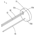
- FIG. 1 is a perspective view of an electronic component mounting package 1 according to an embodiment of the present invention as viewed from a first surface 11a side of a base 11.
- FIG. 5 is a perspective view of the electronic component mounting package 1 as viewed from the fourth surface 11 d side of the base body 11. It is the top view and sectional drawing of the package 1 for electronic components mounting.
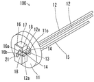
- 3 is a perspective view of the electronic device 100 as viewed from the first surface 11a side of the base 11.
- FIG. 1 is a perspective view of an electronic component mounting package 1 according to an embodiment of the present invention as viewed from the first surface 11a side of a base 11, and FIG. 11 is a perspective view seen from the fourth surface 11d side.
- FIG. 3 is a plan view and a cross-sectional view of the electronic component mounting package 1.
- FIG. 3A is a plan view
- FIG. 3B is a cross-sectional view taken along line AA in FIG.
- FIG. 4 is a perspective view showing the configuration of the electronic device 100 according to this embodiment.
- the electronic component mounting package 1 is a package for mounting an electronic component 21 such as an optical semiconductor element.
- the electronic device 100 is a semiconductor device that receives and transmits optical signals using an optical communication device, and is mounted on the electronic component mounting package 1 and the first surface 11 a of the base 11 of the electronic component mounting package 1.
- the electronic component 21 is comprised.
- the electronic component mounting package 1 is provided between a base 11, a pair of signal terminals 12 made of a linear metal conductor that passes through the base 11 and transmits a high-frequency signal, and a first portion 12 a of the pair of signal terminals 12.
- a high-frequency signal is a signal corresponding to a transmission speed of a semiconductor device of 2.5 Gbps or higher.
- the substrate 11 has a through-hole 11b penetrating in the thickness direction, and has a function of dissipating heat generated by the mounted electronic component 21 to the outside of the electronic component mounting package 1.
- the base 11 is made of a metal having good thermal conductivity, and is close to the thermal expansion coefficient of the electronic component 21, the ceramic wiring substrate 16 or the submount 17 mounted on the electronic device 100, for example, Fe—Ni—Co.
- An iron-based alloy such as an alloy or an Fe—Mn alloy, or a metal such as pure iron is selected. More specifically, there is an SPC (Steel Plate Cold) material of Fe 99.6 mass% -Mn 0.4 mass%.
- the base 11 is made of an Fe—Mn alloy
- the ingot (lumb) is manufactured in a predetermined shape by applying a known metal processing method such as rolling or punching, and the through hole 11b is formed by, for example, drilling. It is formed.
- the shape of the substrate 11 is usually a flat plate having a thickness of 0.5 to 2 mm, and the shape is not particularly limited, but for example, a disk having a diameter of 3 to 10 mm and a radius of 1.5 to 8 mm. For example, a semicircular plate with a part of the circumference cut off, a square plate with a side of 3 to 15 mm, and the like.
- the thickness of the base body 11 may not be uniform. For example, if the thickness of the outer side of the base body 11 is increased, a heat sink such as a housing for housing the electronic device 100 is easily adhered. The generated heat is more easily released to the outside through the substrate 11.
- the thickness of the substrate 11 is preferably 0.5 mm or more and 2 mm or less.
- the bonding conditions such as the bonding temperature when the metal lid for protecting the electronic component 21 is bonded to the first surface 11 a of the metal substrate 11.
- the base body 11 is bent and easily deformed, and the airtightness is easily lowered by the deformation.
- the thickness of the substrate 11 exceeds 2 mm, the thickness of the electronic component mounting package 1 and the electronic device 100 becomes thick, and it becomes difficult to reduce the size.
- the first surface 11a of the base 11 has excellent corrosion resistance, excellent wettability with a bonding material (brazing material) for bonding and fixing the electronic component 21, the wiring board 16, or the lid, and has a thickness of 0. It is preferable that a Ni layer having a thickness of 5 to 9 ⁇ m and an Au layer having a thickness of 0.5 to 5 ⁇ m are sequentially deposited by a plating method. Thereby, it is possible to effectively prevent the base 11 from being oxidatively corroded and to satisfactorily braze (join) the base body 11 to the base 11.
- the submount 17 is provided on the first surface 11a of the base 11, and has a substrate mounting surface parallel to the first surface 11a.
- the submount 17 conducts heat generated by the electronic component 21 mounted on the wiring substrate 16 mounted on the substrate mounting surface to the base 11, for example, from the surface of the base 11. It has a function of radiating heat to the outside of the component mounting package 1.
- the submount 17 may be formed integrally with the base body 11 and may include a cooling member (for example, a Peltier element) that cools the wiring board 16.
- a cooling member for example, a Peltier element
- the submount 17 is made of a metal having good thermal conductivity similar to the base body 11, and is formed in a columnar shape having a substrate mounting surface parallel to the first surface 11a of the base body 11. Is done.
- the wiring board 16 is provided on the board mounting surface of the submount 17, and the electronic component 21 is mounted thereon.
- a signal line conductor 16 a for transmitting a high frequency signal from one signal terminal 12 of the pair of signal terminals 12 to the electronic component 21, and the other signal of the pair of signal terminals 12.
- a signal line conductor 16 b for transmitting a high-frequency signal from the terminal 12 to the electronic component 21 is provided.
- the high-frequency signal transmitted through the pair of signal terminals 12 is a differential signal.
- the wiring board 16 is a wiring conductor including signal line conductors 16a and 16b on an insulating board made of a ceramic insulating material such as an aluminum oxide (alumina: Al 2 O 3 ) sintered body or an aluminum nitride (AlN) sintered body. Is formed. If the insulating substrate is made of, for example, an aluminum oxide sintered body, an organic solvent suitable for raw material powders such as alumina (Al 2 O 3 ), silica (SiO 2 ), calcia (CaO) and magnesia (MgO) is first used.
- alumina Al 2 O 3
- silica SiO 2
- CaO calcia
- MgO magnesia
- a solvent is added and mixed to form a slurry, which is formed into a sheet by a doctor blade method or a calender roll method or the like to obtain a ceramic green sheet (hereinafter also referred to as a green sheet).
- a green sheet is punched into a predetermined shape, and a plurality of sheets are laminated as necessary, and the green sheet is fired at a temperature of about 1600 ° C.
- the wiring conductor including the signal line conductors 16 a and 16 b can be formed by simultaneous firing with the insulating substrate or by forming a metal metallization after the insulating substrate is manufactured, or by vapor deposition after the insulating substrate is manufactured. Alternatively, there is a method of forming by a photolithography method.
- the wiring board 16 mounted on the electronic device 100 is further small, so that the wiring conductor is fine, and in order to increase the alignment accuracy between the wiring conductor and the pair of signal terminals 12.
- a method of forming by vapor deposition or photolithography is preferable, and in this case, the main surface of the insulating substrate may be polished as necessary.
- the signal line conductors 16a and 16b and the pair of signal terminals 12 are electrically connected by a bonding wire 18 provided between the tip of the first portion 12a of the signal terminal 12 and the ends of the signal line conductors 16a and 16b.
- the connection between the signal line conductors 16a and 16b and the electronic component 21 may be a wire connection using a bonding wire, and the terminal provided on the electronic component 21 and the signal line conductors 16a and 16b are directly connected by solder or the like. It may be a bump connection to be joined.
- the bonding wire 18 is a wire member provided between the tip of the first portion 12a of the signal terminal 12 and the ends of the signal line conductors 16a and 16b by a known wire bonding method.
- a gold wire or an aluminum wire can be used as the bonding wire 18.
- the wiring conductor is composed of a conductor layer having a three-layer structure in which, for example, an adhesion metal layer, a diffusion prevention layer, and a main conductor layer are sequentially laminated.
- the adhesion metal layer is made of titanium (Ti), chromium (Cr), tantalum (Ta), niobium (Nb), nickel-chromium (Ni—). Cr) alloy, tantalum nitride (Ta 2 N) or the like is preferably made of at least one metal having a thermal expansion coefficient close to that of ceramics, and the thickness is preferably 0.01 to 0.2 ⁇ m. If the thickness of the adhesion metal layer is less than 0.01 ⁇ m, it tends to be difficult to firmly adhere the adhesion metal layer to the insulating substrate. If the thickness exceeds 0.2 ⁇ m, the adhesion metal layer is caused by internal stress during film formation. There is a tendency to easily peel from the insulating substrate.
- the diffusion preventing layer is made of platinum (Pt), palladium (Pd), rhodium (Rh), nickel (Ni), Ni—Cr alloy, Ti— It is preferably made of at least one metal having good thermal conductivity such as W alloy, and its thickness is preferably 0.05 to 1 ⁇ m. If the thickness of the diffusion preventive layer is less than 0.05 ⁇ m, defects such as pinholes tend to be generated, making it difficult to function as a diffusion preventive layer. If the thickness exceeds 1 ⁇ m, the diffusion preventive layer is caused by internal stress during film formation. Tends to be easily peeled off from the adhesive metal layer. In the case where a Ni—Cr alloy is used for the diffusion preventing layer, the adhesion metal layer can be omitted because the Ni—Cr alloy has good adhesion to the insulating substrate.
- the main conductor layer is preferably made of at least one of gold (Au), copper (Cu), nickel (Ni) and silver (Ag) having a low electric resistance, and the thickness is preferably 0.1 to 5 ⁇ m. If the thickness of the main conductor layer is less than 0.1 ⁇ m, the electric resistance becomes large, and the electric resistance required for the wiring conductor of the wiring substrate 16 tends to be not satisfied. The main conductor layer tends to be easily peeled off from the diffusion preventing layer. Further, since Cu is easily oxidized, a protective layer made of Ni and Au may be coated thereon.
- the pair of signal terminals 12 are formed in a rod shape with a circular cross section, and each first portion 12a is exposed from the first surface 11a of the base 11 and is inserted through the through hole 11b. A portion of the through hole 11b excluding the signal terminal 12 is filled with an insulating material 11c. The length of the first part 12a is, for example, 1 to 5 mm.
- the pair of signal terminals 12 are provided in the through holes 11b such that each first portion 12a protrudes from the first surface 11a of the base body 11 to one side in the thickness direction and is spaced from each other.
- the insulating material 11 c is made of an insulating inorganic dielectric material such as glass or ceramics, and has a function of securing an insulating interval between the signal terminal 12 and the base 11 and fixing the signal terminal 12 in the through hole 11 b of the base 11.
- the insulating material 11c include glasses such as borosilicate glass and soda glass, and those obtained by adding a ceramic filler for adjusting the thermal expansion coefficient and relative dielectric constant to these glasses, and impedance matching. Therefore, the relative dielectric constant is appropriately selected.
- the filler that lowers the dielectric constant include lithium oxide.
- a glass powder is used by a powder pressing method or an extrusion molding method.
- a cylindrical molded body having the inner diameter matched with the outer diameter of the signal terminal 12
- the outer diameter matched with the shape of the through hole 11b, and the signal terminal 12 is inserted into the hole of the molded body and molded.
- the body is inserted into a mold, heated to a predetermined temperature to melt the glass, and then cooled and solidified to form an insulating material 11c having a predetermined shape to which the signal terminal 12 is fixed.
- the through hole 11b is hermetically sealed by the insulating material 11c, and the signal terminal 12 is insulated from the base 11 and fixed by the insulating material 11c, thereby forming a coaxial line structure.
- the insulating material 11c matched to the shape of the through hole 11b is formed in advance, and this is inserted into the through hole 11b, and the signal terminal 12 is passed through the hole of the insulating material 11c, so that the insulating material 11c and the through hole 11b
- the inner surface and the outer surface of the signal terminal 12 and the inner surface of the hole of the insulating material 11c may be joined at the same time.
- the dielectric substrate 13 is formed in a plate shape and is provided between the first portions 12a.
- the dielectric substrate 13 has a second surface 13a and a third surface 13b that are perpendicular to the first surface 11a of the base 11, the side surface abutting against the first surface 11a of the base 11, and the second surface. 13a is provided so as to face one of the first parts 12a, and the third surface 13b is provided so as to face the other of the first parts 12a.
- the dielectric substrate 13 has two first portions 12a on the first surface 11a of the base body 11 in the thickness direction (parallel to the imaginary line connecting the signal terminals 12). It is provided so that it may pinch
- the dielectric substrate 13 is lower in height in the direction orthogonal to the first surface 11a with respect to the first surface 11a of the base body 11 than the first portion 12a.
- the high-frequency signal transmitted through the pair of signal terminals 12 is a differential signal.
- the differential signal is transmitted through two transmission lines that are electromagnetically coupled to each other, so-called pair wirings.
- the pair of signal terminals 12 serve as a pair wiring and transmit a differential signal.
- the insulating material 11c made of a dielectric material exists between the pair of signal terminals 12, so that sufficient electromagnetic coupling can be obtained.
- the electromagnetic coupling becomes weak when the dielectric material is lost.
- the dielectric substrate 13 between the two first parts 12a the electromagnetic coupling between the two first parts 12a can be strengthened.
- the rigidity of the first part 12a is increased.
- the first portion 12a is less likely to be deformed. From this, it is possible to suppress deformation of the first portion 12a that occurs when wire bonding is performed on the tip of the first portion 12a.
- the manufacturing process of the electronic component mounting package 1 and the electronic device 100 and the heat applied to the first portion 12a when the electronic device 100 is operated can prevent the first portion 12a from being deformed. As a result, it is possible to suppress fluctuations in characteristic impedance caused by the deformation of the first portion 12a.
- a portion in the through hole 11 b of the base body 11, that is, the periphery is surrounded by the insulating material 11 c, and the insulating material 11 c is further surrounded by the through hole 11 b of the base body 11.
- stable transmission characteristics can be obtained.
- the capacitance component is reduced, the inductance component is increased, and the transmission characteristic of the high-frequency signal is in the coaxial structure portion. Compared to deterioration. Also, the characteristic impedance is higher than that of the coaxial structure portion in the through hole 11b.
- the transmission characteristic of the first part 12a itself having a high characteristic impedance is deteriorated, and a reflection loss of a high frequency signal is caused by a sudden and large change in the characteristic impedance at the boundary part between the coaxial structure part and the first part 12a in the through hole 11b. Insertion loss and the like increase, and transmission characteristics deteriorate significantly.
- the dielectric substrate 13 between the two first portions 12a it is possible to suppress a decrease in capacitance component and an increase in inductance component, respectively, and a characteristic impedance extending from the coaxial structure portion to the first portion 12a in the through hole 11b. Change can be reduced.
- the tip of the first portion 12a of the signal terminal 12 and the signal line conductors 16a and 16b are connected by the bonding wire 18.
- the portion of the bonding wire 18 through which the high-frequency signal is transmitted has a smaller diameter than the first portion 12a and there is no insulating material in the periphery, so that the capacitance component is further reduced and the inductance component is increased compared to the first portion 12a.
- the transmission characteristics of the high-frequency signal are deteriorated as compared with the coaxial structure portion, and the characteristic impedance is increased. That is, the characteristic impedance is higher in the order of the coaxial structure portion, the first portion 12a, and the bonding wire 18 in the through hole 11b, and changes rapidly at each boundary portion.
- the magnitude of the characteristic impedance of the first portion 12a approaches the coaxial structure portion in the through hole 11b, and therefore the magnitude of the characteristic impedance between the coaxial structure portion in the through hole 11b and the first portion 12a. Can be reduced.
- the difference in characteristic impedance at the boundary portion at the connection portion between the first portion 12a and the bonding wire 18 widens, that is, the change becomes large.
- the dielectric substrate 13 is provided between the two first portions 12a.
- the first portion 12a and the bonding wire 18 are used.
- the change in characteristic impedance at the boundary portion at the connection portion increases, and reflection loss or loss insertion that occurs when a high-frequency signal is transmitted between the first portion 12a and the bonding wire 18 increases.
- the height of the dielectric substrate 13 lower than the first portion 12a, the portion of the first portion 12a adjacent to the dielectric substrate 13, the first portion 12a, the bonding wire 18, and A portion where the dielectric substrate 13 is not adjacent is provided between the connection portions.
- the capacitive component of the portion of the first portion 12a that is not adjacent to the dielectric substrate 13 is smaller than the adjacent portion and larger than the portion of the bonding wire 18 that has a smaller diameter than the first portion 12a. For this reason, the characteristic impedance of the portion of the first portion 12a where the dielectric substrate 13 is not adjacent is higher than that of the adjacent portion and lower than that of the bonding wire 18.
- the dielectric substrate 13 is adjacent by providing a portion where the dielectric substrate 13 of the first portion 12a is not adjacent to the bonding wire 18 between the portion where the dielectric substrate 13 is adjacent.
- the change in characteristic impedance from the first part 12a to the bonding wire 18 can be made gradual as compared with the structure of the prior art. If the change in characteristic impedance is gradual, reflection loss and insertion loss that occur when a high-frequency signal is transmitted can be reduced, and deterioration of transmission characteristics of the high-frequency signal can be suppressed.
- the dielectric substrate 13 may have a width in the direction perpendicular to the imaginary line connecting the first portions 12a larger than the width of the first portions 12a.
- the bonding wire 18 has a large difference in characteristic impedance with the first part 12a, a high inductance component, and a transmission line that is difficult to transmit a high-frequency signal due to a structure in which a ground conductor is not present in the vicinity. It is. Therefore, the length of the bonding wire 18 is preferably as short as possible. In order to shorten the bonding wire 18, it is necessary to shorten the distance between the tip of the first part 12 a and the wiring board 16. To shorten the distance between the tip of the first part 12 a and the wiring board 16, the wiring board is required. It is necessary to reduce the difference in height between the height of 16 (the height of the submount 17) and the tip of the first portion 12a.
- the submount 17 includes a cooling member such as a Peltier element
- the height of the submount 17 is relatively high, and the height of the tip of the first portion 12a is increased in accordance with the height of the submount 17. .
- the portion of the first portion 12a where the transmission characteristics of the high-frequency signal deteriorates becomes longer. Therefore, the effect of providing the dielectric substrate 13 between the two first portions 12a is more exhibited.
- the length of the portion where the dielectric substrate 13 is not adjacent is 10 to 50% with reference to the length of the first portion 12a.
- the thickness of the dielectric substrate 13 (the thickness in the direction parallel to the imaginary line connecting each signal terminal 12) and the height from the first surface 11a of the base 11, that is, the first surface 11a of the base 11 to the first.
- the width of the dielectric substrate 13 in the direction perpendicular to the imaginary line connecting each first portion 12a is the width of the through hole 11b in the direction perpendicular to the imaginary line connecting each first portion 12a (of the insulating material 11c). Width).
- the dielectric substrate 13 may be provided inside the through hole 11b when the electronic component mounting package 1 is viewed in plan from the first surface 11a side of the base 11.
- the dielectric substrate 13 may be provided inside the through hole 11b when the electronic component mounting package 1 is viewed in plan from the first surface 11a side of the base 11.
- it is possible to reduce the stress caused by the difference in thermal expansion coefficient generated between the base 11, the insulating material 11c, and the dielectric substrate 13, and to the insulating material 11c and the dielectric substrate 13 by this stress. It can suppress that a crack or a crack arises.
- a metal material is used for the bonding material 14 for bonding the dielectric substrate 13 and the first portion 12a in order to improve the heat dissipation of the electronic component mounting package 1, the base 11 and the signal terminal 12 are bonded. Electrical short-circuiting by the material 14 can be suppressed.
- a resin material or a ceramic material can be used as long as it is an insulating material so as not to short-circuit between the first parts 12 a, but a ceramic having a high dielectric constant with little deformation due to heat or the like.
- a ceramic material an aluminum oxide sintered body, an aluminum nitride sintered body, a mullite sintered body, a silicon carbide sintered body, a silicon nitride sintered body, a glass ceramic, and the like can be used.
- the dielectric substrate 13 is made of, for example, an aluminum oxide sintered body, a green sheet molded into a sheet shape by a known doctor blade method or calender roll method is used in the same manner as the insulating substrate of the wiring substrate 16. It is manufactured by punching into a shape, stacking a plurality of sheets as necessary, and firing at a temperature of about 1600 ° C.
- the dielectric substrate 13 may be fixed by an adhesive made of a resin material or a glass material on the side surface in contact with the first surface 11a of the base 11, but in order to prevent the dielectric substrate 13 from falling off,
- the surface 13a and one of the first parts 12a may be joined, and the joining material 14 for joining the third face 13b and the other of the first parts 12a may be included.
- the height of the dielectric substrate 13 is made lower than that of the first portion 12a, and the second surface 13a of the dielectric substrate 13 and one of the first portions 12a are bonded by the bonding material 14,
- the bonding material 14 By joining the third surface 13b and the other of the first part 12a, the rigidity of the first part 12a is improved by the dielectric substrate 13, and the tip of the first part 12a to which the dielectric substrate 13 is not joined Stress generated between the dielectric substrate 13 and the dielectric substrate 13 can be suppressed.
- the deformation of the first part 12a can be suppressed, the fluctuation of the characteristic impedance caused by the deformation of the first part 12a can be suppressed, and the dielectric substrate 13 can be cracked or cracked. Can be suppressed. Furthermore, it can suppress that the bonding wire 18 peels from the 1st part 12a. Further, when the bonding wire 18 is connected to the first portion 12a, the dielectric substrate 13 is cracked or cracked by the stress applied to the first portion 12a. The dielectric substrate 13 is not bonded to the first portion 12a. It can be suppressed by moderately deforming the tip and relaxing the stress.
- a brazing material of (Sn—Ag—Cu) alloy or a resin adhesive such as Ag epoxy can be used.
- a metal layer by plating or the like may be provided on both main surfaces (the second surface 13a and the third surface 13b) of the dielectric substrate 13.
- the shape of the tip of each first portion 12a of the pair of signal terminals 12 is not particularly limited, but may be a tapered shape such as a hemispherical shape, a truncated cone shape, or a truncated pyramid shape. Since the tip of each first portion 12a of the pair of signal terminals 12 is tapered, the change in the shape of the transmission path of the high-frequency signal becomes gentle, so the connection portion between the tip of each first portion 12a and the bonding wire 18 , The change in characteristic impedance becomes more gradual.
- the pair of signal terminals 12 is made of a metal conductor such as an Fe—Ni—Co alloy or Fe—Ni alloy.
- a metal conductor such as an Fe—Ni—Co alloy or Fe—Ni alloy.
- the ingots (lumps) are rolled.
- a known metal processing method such as punching or cutting, a wire having a length of 1.5 to 22 mm and a diameter of 0.1 to 1 mm is manufactured.
- the diameter of the pair of signal terminals 12 is 0.15 to 0.25 mm.
- the diameter of the pair of signal terminals 12 is smaller than 0.15 mm, the signal terminals 12 are likely to be bent during handling when the electronic component mounting package 1 is mounted, and workability is likely to be reduced. Also, if the diameter is larger than 0.25 mm, the diameter of the through hole 11b when impedance matching is increased with the diameter of the signal terminal 12, which is not suitable for product miniaturization.
- the second part of the pair of signal terminals 12 is inserted into, for example, an insertion hole provided on the mounting substrate and having a conductor layer on the inner peripheral surface.
- the conductor layer of the insertion hole is electrically connected to the external electric circuit, and the signal terminal 12 functions to transmit an input / output signal between the electronic component 21 and the external electric circuit.
- the ground terminal 15 is joined to the base 11.
- the ground terminal 15 is connected to the ground potential, manufactured in the same manner as the signal terminal 12, and joined to the fourth surface 11d of the base 11 using a joining material (brazing material) or the like.
- a hole may be formed in the fourth surface 11d of the base 11 in advance, and the ground terminal 15 may be bonded to the hole.
- Examples of the electronic component 21 mounted on the electronic apparatus 100 include an optical semiconductor element such as an LD (laser diode) or PD (photodiode), a semiconductor element including a semiconductor integrated circuit element, a crystal resonator, a surface acoustic wave element, or the like. Piezoelectric elements, pressure sensor elements, capacitive elements, resistors, and the like.
- the mounting of the electronic component 21 on the wiring board 16 may be performed by fixing with a conductive bonding material such as a brazing material or a conductive resin.
- a conductive bonding material such as a brazing material or a conductive resin.
- a gold-tin (Au—Sn) alloy or gold-germanium (Au—) is used to fix the wiring board 16.
- a brazing material of Ge) alloy is used as a bonding material.
- a tin-silver (Sn-Ag) alloy or a tin-silver-copper (Sn-Ag-Cu) alloy having a lower melting point is used.
- a brazing material or a resin adhesive such as Ag epoxy that can be cured at a temperature lower than the melting point may be used as the bonding material.
- the wiring substrate 16 may be mounted on the submount 17 after the electronic component 21 is mounted on the wiring substrate 16, and in this case, contrary to the above, it is used when mounting the wiring substrate 16 on the submount 17.
- the melting point of the bonding material may be lowered.
- the paste of the bonding material is printed on the wiring board 16 by using a well-known screen printing method, the bonding material layer is formed by the photolithography method, or the low melting point brazing material to be the bonding material For example, a preform can be placed.
- the lid provided on the first surface 11a of the base 11 as necessary in the electronic device 100 has an outer shape along the outer peripheral region of the base 11, and the electronic component 21 and the wiring on the first surface 11a of the base 11 It has a shape having a space that covers the substrate 16, the submount 17, the first portion 12 a of the signal terminal 12, the dielectric substrate 13, and the like.
- the electronic component 21 is an optical semiconductor element such as an LD (laser diode) or PD (photodiode)
- a window member that transmits light may be provided in a portion of the lid facing the electronic component 21; Instead of the window member, an optical fiber and an optical isolator for preventing return light may be joined.
- the lid is made of a metal such as an Fe—Ni—Co alloy, an Fe—Ni alloy, or an Fe—Mn alloy, and is produced by subjecting these plate materials to a known metal working method such as press working or punching.
- the lid preferably has the same thermal expansion coefficient as the material of the base 11, and the same material as the material of the base 11 is used.
- a flat or lens-shaped glass window member is bonded to a member provided with a hole in a portion facing the electronic component 21 with a low melting point glass or the like.
- the lid is joined to the base 11 by welding such as seam welding or YAG laser welding, or by brazing with a joining material such as Au—Sn brazing material.
- the electronic component mounting package 1 using the circular base body 11 as shown in FIG. 1 has been described as an example, but a box-shaped electronic component mounting package may be used.
- the shape of the dielectric substrate 13 is not limited to a rectangular shape as long as it has a width larger than the width of the first portion 12a, and may be a perfect circle shape, an elliptical shape, a polygonal shape, or the like.
Landscapes
- Physics & Mathematics (AREA)
- Condensed Matter Physics & Semiconductors (AREA)
- General Physics & Mathematics (AREA)
- Electromagnetism (AREA)
- Optics & Photonics (AREA)
- Semiconductor Lasers (AREA)
- Structure Of Printed Boards (AREA)
Abstract
Description
11 基体
11a 第1の面
11b 貫通孔
11c 絶縁材料
11d 第4の面
12 信号端子
12a 信号端子の第1部
13 誘電体基板
13a 第2の面
13b 第3の面
14 接合材
15 接地端子
16 配線基板
16a 信号線路導体
16b 信号線路導体
17 サブマウント
18 ボンディングワイヤ
21 電子部品
100 電子装置
Claims (5)
- 板状に形成され、厚み方向に貫通した貫通孔を有する基体と、
信号を伝送する、線状の金属導体から成る一対の信号端子であって、第1部が前記基体の第1の面から厚み方向の一方側に突出し互いに間を空けて、前記貫通孔に設けられる一対の信号端子と、
前記一対の信号端子の前記第1部の間に設けられる板状の誘電体基板であって、第2の面および第3の面が前記基体の第1の面に対して垂直で、側面が前記基体の第1の面に当接し、前記第2の面が前記第1部の一方に対向し、前記第3の面が前記第1部のもう一方に対向するように設けられ、前記基体の第1の面を基準とする高さが前記第1部よりも低い誘電体基板と、を含むことを特徴とする電子部品搭載用パッケージ。 - 前記第2の面と前記第1部の一方とを接合し、前記第3の面と前記第1部のもう一方とを接合する接合材を含むことを特徴とする請求項1記載の電子部品搭載用パッケージ。
- 前記一対の信号端子は、差動信号を伝送することを特徴とする請求項1または2記載の電子部品搭載用パッケージ。
- 請求項1~3のいずれかに記載の電子部品搭載用パッケージと、
前記基体の一表面に搭載される電子部品と、を含むことを特徴とする電子装置。 - 前記電子部品と、前記一対の信号端子の前記第1部とを電気的に接続するワイヤ部材をさらに含むことを特徴とする請求項4記載の電子装置。
Priority Applications (5)
| Application Number | Priority Date | Filing Date | Title |
|---|---|---|---|
| US15/574,437 US10629505B2 (en) | 2015-08-24 | 2016-08-19 | Electronic component mounting package and electronic device using the same |
| CN201680027658.9A CN107534021B (zh) | 2015-08-24 | 2016-08-19 | 电子部件搭载用封装体以及使用其的电子装置 |
| JP2017536404A JP6412274B2 (ja) | 2015-08-24 | 2016-08-19 | 電子部品搭載用パッケージおよびそれを用いた電子装置 |
| KR1020177032485A KR102046347B1 (ko) | 2015-08-24 | 2016-08-19 | 전자 부품 탑재용 패키지 및 그것을 사용한 전자 장치 |
| EP16839207.4A EP3343602A4 (en) | 2015-08-24 | 2016-08-19 | ASSEMBLING PACKAGING FOR ELECTRONIC COMPONENTS AND ELECTRONIC DEVICE THEREFOR |
Applications Claiming Priority (2)
| Application Number | Priority Date | Filing Date | Title |
|---|---|---|---|
| JP2015164884 | 2015-08-24 | ||
| JP2015-164884 | 2015-08-24 |
Publications (1)
| Publication Number | Publication Date |
|---|---|
| WO2017033860A1 true WO2017033860A1 (ja) | 2017-03-02 |
Family
ID=58100342
Family Applications (1)
| Application Number | Title | Priority Date | Filing Date |
|---|---|---|---|
| PCT/JP2016/074237 Ceased WO2017033860A1 (ja) | 2015-08-24 | 2016-08-19 | 電子部品搭載用パッケージおよびそれを用いた電子装置 |
Country Status (6)
| Country | Link |
|---|---|
| US (1) | US10629505B2 (ja) |
| EP (1) | EP3343602A4 (ja) |
| JP (1) | JP6412274B2 (ja) |
| KR (1) | KR102046347B1 (ja) |
| CN (1) | CN107534021B (ja) |
| WO (1) | WO2017033860A1 (ja) |
Cited By (3)
| Publication number | Priority date | Publication date | Assignee | Title |
|---|---|---|---|---|
| DE102017123342A1 (de) * | 2017-10-09 | 2019-04-11 | Schott Ag | TO-Gehäuse mit hoher Reflexionsdämpfung |
| JP2023504480A (ja) * | 2019-12-03 | 2023-02-03 | インターナショナル・ビジネス・マシーンズ・コーポレーション | 電子回路強化のための漏洩の特性評価および管理 |
| JP2023179694A (ja) * | 2020-09-03 | 2023-12-19 | ショット アクチエンゲゼルシャフト | 電子部品または光電子部品用のヘッダおよびこのようなヘッダを製造するための方法 |
Families Citing this family (4)
| Publication number | Priority date | Publication date | Assignee | Title |
|---|---|---|---|---|
| CN113169130B (zh) * | 2018-11-30 | 2023-10-17 | 京瓷株式会社 | 布线基板、电子部件搭载用封装件以及电子装置 |
| EP3965146B1 (en) | 2020-09-03 | 2025-04-09 | Schott Ag | Header for an electronic component |
| EP3965145B1 (en) | 2020-09-03 | 2025-04-16 | Schott Ag | Transistor header for high-speed optoelectronic package |
| JP7507682B2 (ja) * | 2020-12-28 | 2024-06-28 | 新光電気工業株式会社 | 半導体パッケージ用ステム |
Citations (3)
| Publication number | Priority date | Publication date | Assignee | Title |
|---|---|---|---|---|
| JP2003037329A (ja) * | 2001-07-24 | 2003-02-07 | Hitachi Cable Ltd | 光送信器 |
| JP2011171649A (ja) * | 2010-02-22 | 2011-09-01 | Kyocera Corp | 電子部品搭載用パッケージおよびそれを用いた電子装置 |
| JP2015122466A (ja) * | 2013-12-25 | 2015-07-02 | 京セラ株式会社 | To−can型パッケージ用ヘッダーおよび半導体装置 |
Family Cites Families (16)
| Publication number | Priority date | Publication date | Assignee | Title |
|---|---|---|---|---|
| DE2800696C2 (de) * | 1978-01-09 | 1985-08-22 | Siemens AG, 1000 Berlin und 8000 München | Verfahren zum Herstellen einer Durchführung |
| JP3436009B2 (ja) * | 1996-07-31 | 2003-08-11 | 住友電気工業株式会社 | 光半導体素子 |
| TW449948B (en) * | 1999-06-29 | 2001-08-11 | Rohm Co Ltd | Semiconductor device |
| US6868104B2 (en) * | 2001-09-06 | 2005-03-15 | Finisar Corporation | Compact laser package with integrated temperature control |
| US7254149B2 (en) * | 2002-03-19 | 2007-08-07 | Finisar Corporation | Submount, pedestal, and bond wire assembly for a transistor outline package with reduced bond wire inductance |
| JP3998526B2 (ja) * | 2002-07-12 | 2007-10-31 | 三菱電機株式会社 | 光半導体用パッケージ |
| JP3989350B2 (ja) * | 2002-09-30 | 2007-10-10 | 新光電気工業株式会社 | ガラス端子 |
| JP4617636B2 (ja) * | 2003-03-19 | 2011-01-26 | 住友電気工業株式会社 | 光モジュール |
| JP2004363242A (ja) * | 2003-06-03 | 2004-12-24 | Sumitomo Electric Ind Ltd | 光モジュール |
| JP4470583B2 (ja) | 2004-05-21 | 2010-06-02 | 住友電気工業株式会社 | 光半導体装置 |
| JP4620400B2 (ja) * | 2004-07-16 | 2011-01-26 | 日本特殊陶業株式会社 | 温度センサ、温度センサの製造方法 |
| US7856038B2 (en) * | 2006-03-27 | 2010-12-21 | Sumitomo Electric Industries, Ltd. | Light-emitting module installing thermo-electric controller |
| JP2008211072A (ja) | 2007-02-27 | 2008-09-11 | Mitsubishi Electric Corp | 光モジュール |
| JP2010073776A (ja) * | 2008-09-17 | 2010-04-02 | Rohm Co Ltd | 半導体レーザ装置 |
| EP2371417B1 (de) * | 2010-03-29 | 2019-07-24 | BIOTRONIK SE & Co. KG | Elektrische Durchführung, Verfahren zur Herstellung und Verwendung einer solchen |
| JP5537673B2 (ja) * | 2010-11-29 | 2014-07-02 | 京セラ株式会社 | 電子部品搭載用パッケージおよびそれを用いた電子装置 |
-
2016
- 2016-08-19 CN CN201680027658.9A patent/CN107534021B/zh active Active
- 2016-08-19 KR KR1020177032485A patent/KR102046347B1/ko active Active
- 2016-08-19 WO PCT/JP2016/074237 patent/WO2017033860A1/ja not_active Ceased
- 2016-08-19 EP EP16839207.4A patent/EP3343602A4/en not_active Withdrawn
- 2016-08-19 US US15/574,437 patent/US10629505B2/en active Active
- 2016-08-19 JP JP2017536404A patent/JP6412274B2/ja active Active
Patent Citations (3)
| Publication number | Priority date | Publication date | Assignee | Title |
|---|---|---|---|---|
| JP2003037329A (ja) * | 2001-07-24 | 2003-02-07 | Hitachi Cable Ltd | 光送信器 |
| JP2011171649A (ja) * | 2010-02-22 | 2011-09-01 | Kyocera Corp | 電子部品搭載用パッケージおよびそれを用いた電子装置 |
| JP2015122466A (ja) * | 2013-12-25 | 2015-07-02 | 京セラ株式会社 | To−can型パッケージ用ヘッダーおよび半導体装置 |
Non-Patent Citations (1)
| Title |
|---|
| See also references of EP3343602A4 * |
Cited By (5)
| Publication number | Priority date | Publication date | Assignee | Title |
|---|---|---|---|---|
| DE102017123342A1 (de) * | 2017-10-09 | 2019-04-11 | Schott Ag | TO-Gehäuse mit hoher Reflexionsdämpfung |
| JP2023504480A (ja) * | 2019-12-03 | 2023-02-03 | インターナショナル・ビジネス・マシーンズ・コーポレーション | 電子回路強化のための漏洩の特性評価および管理 |
| JP7641964B2 (ja) | 2019-12-03 | 2025-03-07 | インターナショナル・ビジネス・マシーンズ・コーポレーション | 電子回路強化のための漏洩の特性評価および管理 |
| JP2023179694A (ja) * | 2020-09-03 | 2023-12-19 | ショット アクチエンゲゼルシャフト | 電子部品または光電子部品用のヘッダおよびこのようなヘッダを製造するための方法 |
| JP7690539B2 (ja) | 2020-09-03 | 2025-06-10 | ショット アクチエンゲゼルシャフト | 電子部品または光電子部品用のヘッダおよびこのようなヘッダを製造するための方法 |
Also Published As
| Publication number | Publication date |
|---|---|
| US20180145003A1 (en) | 2018-05-24 |
| JPWO2017033860A1 (ja) | 2018-03-01 |
| KR102046347B1 (ko) | 2019-11-19 |
| EP3343602A1 (en) | 2018-07-04 |
| CN107534021A (zh) | 2018-01-02 |
| EP3343602A4 (en) | 2019-04-03 |
| CN107534021B (zh) | 2020-12-01 |
| US10629505B2 (en) | 2020-04-21 |
| KR20170137153A (ko) | 2017-12-12 |
| JP6412274B2 (ja) | 2018-10-24 |
Similar Documents
| Publication | Publication Date | Title |
|---|---|---|
| JP6412274B2 (ja) | 電子部品搭載用パッケージおよびそれを用いた電子装置 | |
| JP5473583B2 (ja) | 電子部品搭載用パッケージおよびそれを用いた電子装置 | |
| JP5537673B2 (ja) | 電子部品搭載用パッケージおよびそれを用いた電子装置 | |
| JP5409432B2 (ja) | 電子部品搭載用パッケージおよびそれを用いた電子装置 | |
| JP2016189431A (ja) | 電子部品搭載用パッケージおよびそれを用いた電子装置 | |
| JP5616178B2 (ja) | 電子部品搭載用パッケージおよび通信用モジュール | |
| JP2010062512A (ja) | 電子部品搭載用パッケージおよびそれを用いた電子装置 | |
| JP4874298B2 (ja) | 信号端子と信号線路導体との接続構造および電子部品搭載用パッケージならびに電子装置 | |
| JP2009152520A (ja) | 信号端子と信号線路導体との接続構造および電子部品搭載用パッケージならびに電子装置 | |
| JP5004824B2 (ja) | 信号端子と信号線路導体との接続構造および電子部品搭載用パッケージならびに電子装置 | |
| JP5127475B2 (ja) | 接続基板および電子装置 | |
| JP2010245507A (ja) | 電子部品搭載用パッケージおよびそれを用いた電子装置 | |
| JP6431441B2 (ja) | 電子部品搭載用パッケージおよびそれを用いた電子装置 | |
| JP5404484B2 (ja) | 電子部品搭載用パッケージおよびそれを用いた電子装置 | |
| JP5361637B2 (ja) | 電子部品搭載用パッケージおよびそれを用いた電子装置 | |
| JP2009054982A (ja) | 電子部品搭載用パッケージおよびそれを用いた電子装置 | |
| JP5312358B2 (ja) | 電子部品搭載用パッケージおよびそれを用いた電子装置 | |
| JPWO2017188269A1 (ja) | 半導体パッケージおよびそれを用いた半導体装置 | |
| JP5361609B2 (ja) | 電子部品搭載用パッケージおよび電子装置 | |
| JP5409456B2 (ja) | 電子部品搭載用パッケージおよびそれを用いた電子装置 | |
| JP5460089B2 (ja) | 電子部品搭載用パッケージおよびそれを用いた電子装置 | |
| JP5705491B2 (ja) | 電子部品搭載用パッケージおよびそれを用いた電子装置 | |
| JP2014146756A (ja) | 電子部品搭載用パッケージおよびそれを用いた電子装置 | |
| JP2009054750A (ja) | 電子部品搭載用パッケージおよびそれを用いた電子装置 | |
| JP2012227482A (ja) | 電子部品搭載用パッケージおよびそれを用いた電子装置 |
Legal Events
| Date | Code | Title | Description |
|---|---|---|---|
| 121 | Ep: the epo has been informed by wipo that ep was designated in this application |
Ref document number: 16839207 Country of ref document: EP Kind code of ref document: A1 |
|
| ENP | Entry into the national phase |
Ref document number: 20177032485 Country of ref document: KR Kind code of ref document: A |
|
| ENP | Entry into the national phase |
Ref document number: 2017536404 Country of ref document: JP Kind code of ref document: A |
|
| WWE | Wipo information: entry into national phase |
Ref document number: 15574437 Country of ref document: US |
|
| NENP | Non-entry into the national phase |
Ref country code: DE |