WO2017038538A1 - 真空遮断器 - Google Patents
真空遮断器 Download PDFInfo
- Publication number
- WO2017038538A1 WO2017038538A1 PCT/JP2016/074430 JP2016074430W WO2017038538A1 WO 2017038538 A1 WO2017038538 A1 WO 2017038538A1 JP 2016074430 W JP2016074430 W JP 2016074430W WO 2017038538 A1 WO2017038538 A1 WO 2017038538A1
- Authority
- WO
- WIPO (PCT)
- Prior art keywords
- electrode material
- powder
- electrode
- vacuum
- mocr
- Prior art date
- Legal status (The legal status is an assumption and is not a legal conclusion. Google has not performed a legal analysis and makes no representation as to the accuracy of the status listed.)
- Ceased
Links
Images




Classifications
-
- H—ELECTRICITY
- H01—ELECTRIC ELEMENTS
- H01H—ELECTRIC SWITCHES; RELAYS; SELECTORS; EMERGENCY PROTECTIVE DEVICES
- H01H33/00—High-tension or heavy-current switches with arc-extinguishing or arc-preventing means
- H01H33/60—Switches wherein the means for extinguishing or preventing the arc do not include separate means for obtaining or increasing flow of arc-extinguishing fluid
- H01H33/66—Vacuum switches
- H01H33/664—Contacts; Arc-extinguishing means, e.g. arcing rings
-
- C—CHEMISTRY; METALLURGY
- C22—METALLURGY; FERROUS OR NON-FERROUS ALLOYS; TREATMENT OF ALLOYS OR NON-FERROUS METALS
- C22C—ALLOYS
- C22C27/00—Alloys based on rhenium or a refractory metal not mentioned in groups C22C14/00 or C22C16/00
- C22C27/04—Alloys based on tungsten or molybdenum
-
- C—CHEMISTRY; METALLURGY
- C22—METALLURGY; FERROUS OR NON-FERROUS ALLOYS; TREATMENT OF ALLOYS OR NON-FERROUS METALS
- C22C—ALLOYS
- C22C27/00—Alloys based on rhenium or a refractory metal not mentioned in groups C22C14/00 or C22C16/00
- C22C27/06—Alloys based on chromium
-
- C—CHEMISTRY; METALLURGY
- C22—METALLURGY; FERROUS OR NON-FERROUS ALLOYS; TREATMENT OF ALLOYS OR NON-FERROUS METALS
- C22C—ALLOYS
- C22C30/00—Alloys containing less than 50% by weight of each constituent
- C22C30/02—Alloys containing less than 50% by weight of each constituent containing copper
-
- C—CHEMISTRY; METALLURGY
- C22—METALLURGY; FERROUS OR NON-FERROUS ALLOYS; TREATMENT OF ALLOYS OR NON-FERROUS METALS
- C22C—ALLOYS
- C22C9/00—Alloys based on copper
-
- H—ELECTRICITY
- H01—ELECTRIC ELEMENTS
- H01H—ELECTRIC SWITCHES; RELAYS; SELECTORS; EMERGENCY PROTECTIVE DEVICES
- H01H1/00—Contacts
- H01H1/02—Contacts characterised by the material thereof
- H01H1/0203—Contacts characterised by the material thereof specially adapted for vacuum switches
- H01H1/0206—Contacts characterised by the material thereof specially adapted for vacuum switches containing as major components Cu and Cr
-
- H—ELECTRICITY
- H01—ELECTRIC ELEMENTS
- H01H—ELECTRIC SWITCHES; RELAYS; SELECTORS; EMERGENCY PROTECTIVE DEVICES
- H01H33/00—High-tension or heavy-current switches with arc-extinguishing or arc-preventing means
- H01H33/60—Switches wherein the means for extinguishing or preventing the arc do not include separate means for obtaining or increasing flow of arc-extinguishing fluid
- H01H33/66—Vacuum switches
- H01H33/662—Housings or protective screens
-
- H—ELECTRICITY
- H02—GENERATION; CONVERSION OR DISTRIBUTION OF ELECTRIC POWER
- H02B—BOARDS, SUBSTATIONS OR SWITCHING ARRANGEMENTS FOR THE SUPPLY OR DISTRIBUTION OF ELECTRIC POWER
- H02B13/00—Arrangement of switchgear in which switches are enclosed in, or structurally associated with, a casing, e.g. cubicle
- H02B13/02—Arrangement of switchgear in which switches are enclosed in, or structurally associated with, a casing, e.g. cubicle with metal casing
- H02B13/035—Gas-insulated switchgear
-
- B—PERFORMING OPERATIONS; TRANSPORTING
- B22—CASTING; POWDER METALLURGY
- B22F—WORKING METALLIC POWDER; MANUFACTURE OF ARTICLES FROM METALLIC POWDER; MAKING METALLIC POWDER; APPARATUS OR DEVICES SPECIALLY ADAPTED FOR METALLIC POWDER
- B22F1/00—Metallic powder; Treatment of metallic powder, e.g. to facilitate working or to improve properties
- B22F1/05—Metallic powder characterised by the size or surface area of the particles
-
- B—PERFORMING OPERATIONS; TRANSPORTING
- B22—CASTING; POWDER METALLURGY
- B22F—WORKING METALLIC POWDER; MANUFACTURE OF ARTICLES FROM METALLIC POWDER; MAKING METALLIC POWDER; APPARATUS OR DEVICES SPECIALLY ADAPTED FOR METALLIC POWDER
- B22F1/00—Metallic powder; Treatment of metallic powder, e.g. to facilitate working or to improve properties
- B22F1/05—Metallic powder characterised by the size or surface area of the particles
- B22F1/052—Metallic powder characterised by the size or surface area of the particles characterised by a mixture of particles of different sizes or by the particle size distribution
-
- B—PERFORMING OPERATIONS; TRANSPORTING
- B22—CASTING; POWDER METALLURGY
- B22F—WORKING METALLIC POWDER; MANUFACTURE OF ARTICLES FROM METALLIC POWDER; MAKING METALLIC POWDER; APPARATUS OR DEVICES SPECIALLY ADAPTED FOR METALLIC POWDER
- B22F9/00—Making metallic powder or suspensions thereof
- B22F9/02—Making metallic powder or suspensions thereof using physical processes
- B22F9/04—Making metallic powder or suspensions thereof using physical processes starting from solid material, e.g. by crushing, grinding or milling
- B22F2009/043—Making metallic powder or suspensions thereof using physical processes starting from solid material, e.g. by crushing, grinding or milling by ball milling
-
- B—PERFORMING OPERATIONS; TRANSPORTING
- B22—CASTING; POWDER METALLURGY
- B22F—WORKING METALLIC POWDER; MANUFACTURE OF ARTICLES FROM METALLIC POWDER; MAKING METALLIC POWDER; APPARATUS OR DEVICES SPECIALLY ADAPTED FOR METALLIC POWDER
- B22F2201/00—Treatment under specific atmosphere
- B22F2201/20—Use of vacuum
-
- B—PERFORMING OPERATIONS; TRANSPORTING
- B22—CASTING; POWDER METALLURGY
- B22F—WORKING METALLIC POWDER; MANUFACTURE OF ARTICLES FROM METALLIC POWDER; MAKING METALLIC POWDER; APPARATUS OR DEVICES SPECIALLY ADAPTED FOR METALLIC POWDER
- B22F2301/00—Metallic composition of the powder or its coating
- B22F2301/20—Refractory metals
-
- B—PERFORMING OPERATIONS; TRANSPORTING
- B22—CASTING; POWDER METALLURGY
- B22F—WORKING METALLIC POWDER; MANUFACTURE OF ARTICLES FROM METALLIC POWDER; MAKING METALLIC POWDER; APPARATUS OR DEVICES SPECIALLY ADAPTED FOR METALLIC POWDER
- B22F2304/00—Physical aspects of the powder
- B22F2304/10—Micron size particles, i.e. above 1 micrometer up to 500 micrometer
-
- B—PERFORMING OPERATIONS; TRANSPORTING
- B22—CASTING; POWDER METALLURGY
- B22F—WORKING METALLIC POWDER; MANUFACTURE OF ARTICLES FROM METALLIC POWDER; MAKING METALLIC POWDER; APPARATUS OR DEVICES SPECIALLY ADAPTED FOR METALLIC POWDER
- B22F2998/00—Supplementary information concerning processes or compositions relating to powder metallurgy
- B22F2998/10—Processes characterised by the sequence of their steps
-
- B—PERFORMING OPERATIONS; TRANSPORTING
- B22—CASTING; POWDER METALLURGY
- B22F—WORKING METALLIC POWDER; MANUFACTURE OF ARTICLES FROM METALLIC POWDER; MAKING METALLIC POWDER; APPARATUS OR DEVICES SPECIALLY ADAPTED FOR METALLIC POWDER
- B22F2999/00—Aspects linked to processes or compositions used in powder metallurgy
-
- B—PERFORMING OPERATIONS; TRANSPORTING
- B22—CASTING; POWDER METALLURGY
- B22F—WORKING METALLIC POWDER; MANUFACTURE OF ARTICLES FROM METALLIC POWDER; MAKING METALLIC POWDER; APPARATUS OR DEVICES SPECIALLY ADAPTED FOR METALLIC POWDER
- B22F3/00—Manufacture of workpieces or articles from metallic powder characterised by the manner of compacting or sintering; Apparatus specially adapted therefor ; Presses and furnaces
- B22F3/12—Both compacting and sintering
- B22F3/14—Both compacting and sintering simultaneously
- B22F3/15—Hot isostatic pressing
-
- B—PERFORMING OPERATIONS; TRANSPORTING
- B22—CASTING; POWDER METALLURGY
- B22F—WORKING METALLIC POWDER; MANUFACTURE OF ARTICLES FROM METALLIC POWDER; MAKING METALLIC POWDER; APPARATUS OR DEVICES SPECIALLY ADAPTED FOR METALLIC POWDER
- B22F9/00—Making metallic powder or suspensions thereof
- B22F9/02—Making metallic powder or suspensions thereof using physical processes
- B22F9/04—Making metallic powder or suspensions thereof using physical processes starting from solid material, e.g. by crushing, grinding or milling
-
- H—ELECTRICITY
- H01—ELECTRIC ELEMENTS
- H01H—ELECTRIC SWITCHES; RELAYS; SELECTORS; EMERGENCY PROTECTIVE DEVICES
- H01H33/00—High-tension or heavy-current switches with arc-extinguishing or arc-preventing means
- H01H33/60—Switches wherein the means for extinguishing or preventing the arc do not include separate means for obtaining or increasing flow of arc-extinguishing fluid
- H01H33/66—Vacuum switches
- H01H33/662—Housings or protective screens
- H01H33/66207—Specific housing details, e.g. sealing, soldering or brazing
- H01H2033/66223—Details relating to the sealing of vacuum switch housings
-
- H—ELECTRICITY
- H01—ELECTRIC ELEMENTS
- H01H—ELECTRIC SWITCHES; RELAYS; SELECTORS; EMERGENCY PROTECTIVE DEVICES
- H01H2201/00—Contacts
- H01H2201/022—Material
- H01H2201/03—Composite
-
- H—ELECTRICITY
- H01—ELECTRIC ELEMENTS
- H01H—ELECTRIC SWITCHES; RELAYS; SELECTORS; EMERGENCY PROTECTIVE DEVICES
- H01H33/00—High-tension or heavy-current switches with arc-extinguishing or arc-preventing means
- H01H33/60—Switches wherein the means for extinguishing or preventing the arc do not include separate means for obtaining or increasing flow of arc-extinguishing fluid
- H01H33/66—Vacuum switches
- H01H33/662—Housings or protective screens
- H01H33/66207—Specific housing details, e.g. sealing, soldering or brazing
Definitions
- the present invention relates to a vacuum circuit breaker.
- the present invention relates to a vacuum circuit breaker for phase matching equipment such as a reactor and a capacitor bank.
- VEBs vacuum circuit breakers
- capacitor bank switching phenomenon causes high frequency large current of about 5 times rated current at the time of turning on, causing roughening due to electrode welding due to preceding discharge, and doubles system voltage at the time of disconnection thereafter Because the high voltage is applied, re-ignition due to the drop of the withstand voltage due to the roughening becomes a problem.
- the vacuum circuit breaker for capacitor bank switching since it is opened and closed frequently once a day, the electrode roughness by the rush current at the time of turning on is accumulated. For this reason, in a vacuum circuit breaker for capacitor switching applications, the breaking speed and the gap length (distance between electrodes) at the time of breaking are increased in order to improve the withstand voltage performance between the breaker poles.
- the operating force for opening and closing the vacuum circuit breaker is increased, and the operating device for opening and closing the vacuum circuit breaker may be enlarged.
- An object of the present invention is to provide a technology that contributes to the reduction of the interrupting speed of the vacuum circuit breaker or the gap length at the time of interrupting.
- One aspect of the vacuum circuit breaker of the present invention for achieving the above object is a vacuum circuit breaker in which a vacuum interrupter is accommodated in a container in which an insulating gas is sealed, and the vacuum interrupter comprises an insulating cylinder and both ends of the insulating cylinder.
- a vacuum vessel constituted by a sealing metal fitting for sealing the part, and a pair of contact points which are housed in the vacuum vessel and which are separable to each other and fixed to the conducting shaft, and at least one of the contacts
- the electrode material of the present invention is an electrode material having a Cu phase and a solid solution particle phase containing a solid solution of Cr, a heat resistant element of any of Mo, W, Ta, Nb, V, and Zr, and the electrode material Containing 20 to 70% of Cu, 1.5 to 64% of Cr, 6 to 76% of a heat-resistant element by weight ratio to an electrode material, and having an average particle diameter of 20 ⁇ m of solid solution particles contained in the electrode material It is below.
- Another aspect of the vacuum circuit breaker of the present invention for achieving the above object is that, in the vacuum circuit breaker, the dispersion state index of the solid solution particles in the electrode material is 2.0 or less.
- FIG. 1 is a schematic cross-sectional view of a vacuum circuit breaker according to an embodiment of the present invention. It is a flowchart of the manufacturing method of the electrode material which concerns on embodiment of this invention.
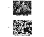
- A Electron micrograph of mixed powder of Mo powder and Cr powder
- (A) Cross-sectional micrograph (magnification x400) of the electrode material of Example 1
- (b) Cross-sectional micrograph (magnification x 800) of the electrode material of Example 1
- B Cross-sectional structure SEM image (magnification ⁇ 2000) of the electrode material of Example 1.
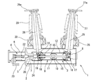
- FIG. 1 is a longitudinal sectional view of a vacuum circuit breaker 1 according to an embodiment of the present invention.
- the vacuum circuit breaker 1 has a ground tank 2 (for example, a container), a vacuum interrupter 3 housed in the ground tank 2, and an operation mechanism 4 for opening and closing the vacuum interrupter 3.
- a ground tank 2 for example, a container
- a vacuum interrupter 3 housed in the ground tank 2
- an operation mechanism 4 for opening and closing the vacuum interrupter 3.
- the ground tank 2 is, for example, a cylindrical metal container and accommodates the vacuum interrupter 3.
- the ground tank 2 is filled with an insulating gas such as SF 6 gas or dry air.
- An operation box 6 is attached to one end of the ground tank 2 via a support plate 5, and an operation mechanism 4 is provided in the operation box 6.
- the insulating support cylinder 7 is supported by the support plate 5 at one end in the horizontal direction in the ground tank 2, and the support insulator 8 is supported at the other end in the ground tank 2.
- the vacuum interrupter 3 is configured by housing a pair of contacts (the fixed electrode 10 and the movable electrode 11) in the vacuum vessel 9 so as to be capable of coming into and coming out of contact with each other.
- the vacuum vessel 9 is constituted by sealing metal fittings 13 and 14 which seal both openings of the insulating cylinder 12 and the insulating cylinder 12.
- An intermediate shield 15 is provided in the vacuum vessel 9 so as to cover the fixed electrode 10 and the movable electrode 11.
- the fixed electrode 10 is fixed to one end of a fixed lead 16 (for example, corresponding to a conduction axis).
- the other end of the fixed lead 16 extends from the end face of the vacuum vessel 9 and is connected to the fixed contact case 17.
- the movable electrode 11 is fixed to one end of a movable lead 18 (for example, corresponding to a conduction axis).
- the other end of the movable lead 18 extends from the end face of the vacuum vessel 9 and is connected to the movable contact case 19.
- an insulating rod 20 is provided at the other end of the movable lead 18, and the insulating rod 20 is connected to the operation mechanism 4.
- a bellows 21 is provided in the vacuum vessel 9 at the insertion portion of the movable lead 18, and the movable lead 18 is movable in the axial direction with the vacuum vessel 9 maintained in vacuum. .
- the operation mechanism 4 is connected to the movable lead 18 via the insulating rod 20, and moves the movable lead 18 in the axial direction.
- the operating mechanism 4 is provided with a pressure contact spring 22.
- the pressure contact spring 22 biases the movable lead 18 in the direction of the fixed lead 16 and fixes it.
- a predetermined contact pressure is applied between the electrode 10 and the movable electrode 11.
- An operating lever 23 is connected to the operating mechanism 4, and the operating mechanism 4 moves the movable lead 18 in the axial direction according to the movement of the operating lever 23.
- a stationary contact case 17 is supported by the support insulator 8.
- the conductor 25 is connected to the fixed side contact case 17.
- the movable side contact case 19 is supported by the insulating support cylinder 7 via the insulating support 24.
- a conductor 26 is connected to the movable contact case 19.
- the conductor 25 is provided in a state of protruding from the ground tank 2.
- a bushing 27 is provided around the conductor 25, and the bushing 27 is supported by the ground tank 2.
- a bushing terminal 27 a electrically connected to the conductor 25 is provided at an upper end portion of the bushing 27.
- a bushing current transformer 28 is provided at the connection between the bushing 27 and the ground tank 2.
- the conductor 26 is provided so as to protrude from the ground tank 2.
- a bushing 29 is provided around the conductor 26, and the bushing 29 is supported by the ground tank 2.
- a bushing terminal 29 a electrically connected to the conductor 26 is provided at the upper end of the bushing 29.
- a bushing current transformer 30 is provided at the connection between the bushing 29 and the ground tank 2.
- the vacuum circuit breaker 1 is characterized in that an electrode made of an electrode material excellent in withstand voltage performance is used as at least one of the fixed electrode 10 and the movable electrode 11.
- an electrode made of an electrode material excellent in withstand voltage performance is used as at least one of the fixed electrode 10 and the movable electrode 11.
- a method of manufacturing an electrode material used as the fixed electrode 10 and the movable electrode 11 will be described in detail.
- the details of the electrode material are described in the specification of Japanese Patent Application No. 2015-528797.
- the average particle diameter, the median diameter d50 and the volume relative particle amount show values measured by a laser diffraction type particle size distribution measuring apparatus (Cirrus: Cirrus 1090 L).
- the inventors examined the correlation between the occurrence of reignition and the distribution of heat-resistant elements (Mo, Cr, etc.) and Cu. As a result, by observing the electrode surface where the reignition occurred, it is found that there are many minute projections (eg, minute projections of several tens ⁇ m to several hundreds ⁇ m) in the Cu region having a melting point lower than that of the heat-resistant element. I found it. Since a high electric field is generated at the tip of this projection, it may be a factor to lower the blocking performance and the withstand voltage performance. The formation of the projection is presumed to be due to the electrode being melted and welded by the applied current, and the melted portion being pulled off at the time of the subsequent current interruption.
- minute projections eg, minute projections of several tens ⁇ m to several hundreds ⁇ m
- the particle size of the heat-resistant element in the electrode is made smaller and finely dispersed, and the Cu region in the electrode surface is finely uniformed. It has been found that the dispersion suppresses the occurrence of minute projections in the Cu region and reduces the occurrence probability of reignition.
- particles of the heat-resistant element on the surface of the electrode are broken by repetition of opening and closing of the contact, and they become fine particles and are separated from the electrode surface to cause dielectric breakdown.
- the inventors achieved the present invention as a result of intensive studies on the particle diameter of the heat-resistant element, the dispersibility of Cu, the voltage resistance of the electrode of the vacuum interrupter, and the like.
- the electrode material of the vacuum circuit breaker according to the embodiment of the present invention is an electrode material in which particles containing Cr are miniaturized and uniformly dispersed, and a Cu structure which is a high-conductivity component is also finely and uniformly dispersed.
- the heat-resistant elements are, for example, molybdenum (Mo), tungsten (W), tantalum (Ta), niobium (Nb), vanadium (V), zirconium (Zr), beryllium (Be), hafnium (Hf), iridium (Ir) Elements selected from elements such as platinum (Pt), titanium (Ti), silicon (Si), rhodium (Rh) and ruthenium (Ru) can be used alone or in combination. In particular, it is preferable to use Mo, W, Ta, Nb, V, or Zr, in which the effect of refining Cr particles is remarkable.
- the average particle diameter of the heat-resistant element powder is, for example, 2 to 20 ⁇ m, more preferably 2 to 10 ⁇ m, to thereby form particles containing Cr (including a solid solution of the heat-resistant element and Cr).
- An electrode material having a finely divided and uniformly dispersed composition can be obtained.
- the Cr is contained in an amount of 1.5 to 64% by weight, more preferably 4 to 15% by weight based on the electrode material, thereby improving the withstand voltage performance and current interrupting performance of the electrode without impairing the mechanical strength and the processability. It can be done.
- the particle size of the Cr powder is, for example, -48 mesh (less than 300 ⁇ m), more preferably -100 mesh (less than 150 ⁇ m), still more preferably -325 mesh (less than 45 ⁇ m) By so setting, it is possible to obtain an electrode material excellent in withstand voltage performance and current interruption performance.
- the particle size of the Cr powder By setting the particle size of the Cr powder to -100 mesh, it is possible to reduce the amount of residual Cr that causes the particle size of Cu infiltrated into the electrode to increase.
- a Cr powder with a small particle diameter in terms of dispersing the particles containing Cr which has been finely divided in the electrode, but as the Cr particles are made finer, the oxygen content contained in the electrode increases The current interrupting performance is reduced.
- the increase in the oxygen content of the electrode material by reducing the particle size of the Cr particles is considered to be caused by the oxidation of the Cr when the Cr is finely pulverized.
- Cr powder having a particle size of less than -325 mesh may be used, and it is possible to refine in the electrode
- the contact resistance of the electrode can be reduced without impairing the withstand voltage performance and the current blocking performance.
- the content of Cu contained in the electrode material is determined by a Cu infiltration process which will be described in detail later, the total of the heat resistant element, Cr and Cu added to the electrode material is 100 It does not exceed% by weight.
- the heat-resistant element powder for example, Mo powder
- the Cr powder are mixed.
- the average particle size of the Mo powder and the Cr powder is not particularly limited, but the average particle size of the Mo powder is 2 to 20 ⁇ m, and the particle size of the Cr powder is -100 mesh.
- the Mo powder and the Cr powder are mixed so that the weight ratio by weight of Cr to Mo1 is 4 or less, more preferably Cr to Mo1 is 1/3 or less. Electrode material can be manufactured.
- the mixed powder of Mo powder and Cr powder (hereinafter referred to as mixed powder) obtained in the mixing step S1 is filled in a container (for example, an alumina container) which does not react with Mo and Cr,
- the pre-sintering is performed at a predetermined temperature (for example, 1250 ° C. to 1500 ° C.) in a non-oxidizing atmosphere (hydrogen atmosphere, vacuum atmosphere or the like).
- a MoCr solid solution in which Mo and Cr mutually diffuse as a solid solution is obtained.
- the sintering temperature and time of the temporary sintering step S2 are selected so that the peak corresponding to at least Mo element disappears by X-ray diffraction measurement of the solid solution of MoCr. Be done.
- the mixed powder may be pressure-formed (press processing) before the pre-sintering.
- pressure forming By pressure forming, mutual diffusion of Mo and Cr is promoted, and the temporary sintering time can be shortened, or the temporary sintering temperature can be reduced.
- the pressure at the time of pressure molding is not particularly limited, but preferably 0.1 t / cm 2 or less.
- the MoCr solid solution is pulverized using a pulverizer (for example, a planetary ball mill) to obtain a MoCr solid solution powder (hereinafter referred to as MoCr powder).
- the pulverizing atmosphere in the pulverizing step S3 is preferably a non-oxidative atmosphere, but may be pulverized in the atmosphere.
- the grinding conditions may be such that the particles (secondary particles) in which the MoCr solid solution particles are bonded to each other are ground. In the grinding of the MoCr solid solution, the average particle size of the MoCr solid solution particles becomes smaller as the grinding time is longer.
- MoCr particles (more preferably, particles with a particle diameter of 30 ⁇ m or less (more preferably, particles with a particle diameter of 20 ⁇ m or less) have a particle size of 50% or more). It is possible to obtain an electrode material in which particles in which Mo and Cr are mutually dissolved in solid solution and Cu structure are uniformly dispersed.
- the MoCr powder is formed. Molding of the MoCr powder is performed, for example, by pressure molding at a pressure of 2 t / cm 2 .
- main sintering of the formed MoCr powder is performed to obtain a MoCr sintered body (MoCr skeleton). This sintering is performed, for example, by sintering a compact of MoCr powder in a vacuum atmosphere at 1150 ° C. for 2 hours.
- the main sintering step S5 is a step of obtaining a denser MoCr sintered body by deformation and bonding of the MoCr powder.
- Sintering of the MoCr powder is preferably performed under the temperature conditions of the following Cu infiltration step S6, for example, at a temperature of 1150 ° C. or higher.
- the sintering temperature of the present invention is higher than the temperature at the time of Cu infiltration and at a temperature not higher than the melting point of Cr, preferably in the range of 1150 to 1500 ° C., densification of the MoCr particles proceeds and MoCr particles Degassing proceeds well.
- the obtained MoCr sintered body may be subjected to HIP (hot isostatic pressing) treatment.
- HIP hot isostatic pressing
- the HIP process is, for example, placing the MoCr sintered body in a stainless steel cylindrical container (height 11 mm, inner diameter ⁇ 62 mm, thickness 5 mm) in a stainless steel container and vacuum sealing, and then 1050 ° C.-70 MPa (HIP processing device) HIP treatment is performed for 0.714 ton / cm 2 ) -2 hours.
- Cu is infiltrated into the MoCr sintered body.
- Infiltration of Cu is performed, for example, by placing a Cu plate material on a MoCr sintered body, and holding the same in a non-oxidizing atmosphere at a temperature higher than the melting point of Cu for a predetermined time (for example, 1150 ° C. for 2 hours).
- the mixed powder of Mo powder and Cr powder was transferred into an alumina container, and the mixed powder was temporarily sintered at 1250 ° C. for 3 hours in a vacuum heating furnace.
- the degree of vacuum of the vacuum heating furnace after sintering for 3 hours at 1250 ° C. was 3.5 ⁇ 10 ⁇ 3 Pa.
- the degree of vacuum after maintaining for a predetermined time at the pre-sintering temperature is 5 ⁇ 10 ⁇ 3 Pa or less, the oxygen content of the electrode material produced using the obtained pre-sintered body decreases, and the electrode There is no loss in the current interrupting performance of the material.
- the MoCr temporary sintered body was taken out of the vacuum heating furnace, and was pulverized for 10 minutes using a planetary ball mill to obtain MoCr powder.
- the MoCr powder was subjected to X-ray diffraction measurement, and temporary sintering was performed to confirm that the Mo element and the Cr element were in solid phase diffusion with each other, and the Mo and Cr were dissolved.
- X-ray diffraction (XRD) measurement of the MoCr powder was performed to determine the crystal constant of the MoCr powder.
- FIG. 3 (a) is an electron micrograph of mixed powder of Mo powder and Cr powder.
- FIG. 3 (b) is an electron micrograph of MoCr powder.
- a relatively large powder having a particle diameter of about 45 ⁇ m could not be confirmed, and it was confirmed that Cr did not exist in the raw material state (size).
- the average particle size (median diameter d50) of the MoCr powder was 15.1 ⁇ m.
- the MoCr powder obtained in the pulverizing step is pressure-molded at a pressure of 2 t / cm 2 using a press to form a compact, and the compact is sintered at 1150 ° C. for 2 hours in a vacuum atmosphere. Then, a MoCr sintered body was produced.
- the region (white portion) that appears relatively white is an alloy structure in which Mo and Cr are in solid solution, and the portion (grey portion) that appears relatively black is a Cu structure.
- the fine alloy structure (white portion) of 1 to 10 ⁇ m was finely dispersed uniformly. Also, the Cu structure was uniformly dispersed without being unevenly distributed.
- N L n L / L (2)
- N S n S / S (3) dm: average particle size, ⁇ : pi,
- N L Number of particles per unit length hit by any straight line on the cross-sectional structure,
- N S number of particles contained per unit area hit in any measurement area,
- n L the number of particles hit by any straight line on the cross-sectional structure,
- L Arbitrary straight line length on cross-sectional structure,
- n S the number of particles contained in any measurement area, S: Area of Arbitrary Measurement Area Specifically, using the SEM image of FIG.
- n L and n S were divided by L and S, respectively, to obtain N L and N S. Further, by substituting the N L and N S in (1) to determine the average particle diameter dm.
- the average particle diameter dm of the MoCr particles of the electrode material of Example 1 was 3.8 ⁇ m.
- the average particle diameter of the MoCr powder obtained by temporarily sintering the mixed powder at 1250 ° C. for 3 hours and grinding it using a planetary ball mill was 15.7 ⁇ m.
- the cross section after Cu infiltration was observed, and the average particle diameter of MoCr particles determined from the Fullman's equation was 3.8 ⁇ m, so it is considered that the refinement of MoCr particles further progressed in the Cu infiltration step S6 .
- the characteristics of the electrode material are influenced not only by how much MoCr particles are present in the electrode material, and by what size the particle size of the MoCr particles is, but by how uniformly the MoCr particles are dispersed. Ru.
- the dispersion state index of the MoCr particles in the electrode material of Example 1 was calculated from the SEM images of FIGS. 5 (a) and 5 (b) to evaluate the micro dispersion state of the electrode structure.
- the dispersion state index was calculated according to the method described in JP-A-4-74924.
- the distance between the centers of gravity of the MoCr particles is measured 100 using the SEM image of FIG. 5 (b), and the average value ave.
- the dispersion state index CV was determined by substituting X and ⁇ into the equation (4).
- CV ⁇ / ave. X ... (4)
- the X was 5.25 ⁇ m
- the standard deviation ⁇ was 3.0 ⁇ m
- the dispersion state index CV was 0.57.
- Table 1 shows manufacturing conditions and withstand voltage performance of Example 1-8.
- the withstand voltage performance is indicated by a relative value where the withstand voltage performance of the electrode material of Comparative Example B is 1.
- the electrode material of the reference examples 1 and 2 is an electrode material manufactured on the conditions from which the calcination conditions in temporary sintering process S2 differ.
- the electrode material according to Comparative Examples A and B is an electrode material according to the prior art, and a mixed powder of Mo powder and Cr powder is pressure-molded at 2 t / cm 2 , and the obtained molded body is 1200 ° C.
- the resultant sintered body is infiltrated with Cu (1150 ° C. for 2 hours). As shown in FIG.
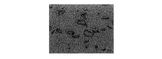
- the electrode material of Comparative Example A has a structure in which Cu (black portion) having a particle size of 20 to 60 ⁇ m is dispersed in 1 to 10 ⁇ m of fine MoCr solid solution particles (white portion). The It is presumed that this is a result of the infiltration of Cu into the void portion generated in the process in which Cr particles are refined by Mo particles and Cr diffuses into Mo particles by the diffusion mechanism and Cr and Mo form a solid solution structure. Ru.
- Example 1-8 shown in Table 1 the electrode material of Example 1-8 is an electrode material having excellent withstand voltage performance as compared with Comparative Examples A and B. Moreover, it turns out that the withstand voltage performance of electrode material is improving as the ratio of the heat-resistant element contained in electrode material increases.
- the electrode material of Example 1-8 includes a mixing step of mixing the heat-resistant element powder and the Cr powder, a pre-sintering step of temporarily sintering the mixture of the heat-resistant element powder and the Cr powder, A grinding process to grind, a main sintering process to sinter a powder obtained by grinding a temporary sintered body, and a Cu infiltration process to infiltrate Cu into a sintered body (skeleton) obtained in the main sintering process
- the alloy composition can be controlled so that the particles in which the heat-resistant element and Cr are mutually dissolved in solution are finely dispersed and uniformly dispersed, and the Cu portion which is a high conductor component is also finely and uniformly dispersed. .
- a vacuum interrupter (hereinafter referred to as a vacuum interrupter of Example 1) was constructed using the electrode material of Example 1 as an electrode contact material (fixed electrode and movable electrode), and the insulation recovery performance of the vacuum interrupter was evaluated.
- Table 2 shows the conditions of the electrode contact material and the conditions of the operating device.
- FIG. 7 shows characteristics of insulation recovery characteristics of the vacuum interrupter of the first embodiment and the vacuum interrupts of the first and second comparison examples.
- the vacuum interrupter of Comparative Example 1 is a conventional vacuum interrupter, and is a vacuum interrupter provided with a CuCr electrode material for the fixed electrode and the movable electrode, having a breaking speed of 3.0 m / s and a breaking gap length of 60 mm.
- the CuCr electrode material is an electrode material manufactured using the same material (Cr powder) as the electrode material of Example 1, and is an electrode material manufactured by sintering Cu and then infiltrating Cu.
- the vacuum interrupter of Comparative Example 2 is a vacuum interrupter provided with the same CuCr electrode material as the vacuum interrupter of Comparative Example 1, and the interrupting speed and the interrupting gap length are made the same as the vacuum interrupter of Example 1. It is a vacuum interrupter.
- the vacuum interrupter of Example 1 has the same insulation recovery characteristics as the vacuum interrupter of Comparative Example 1. That is, as shown in Table 2, the vacuum interrupter of Example 1 reduces the breaking speed by 50% and reduces the gap length at the breaking time by 33% as compared with the vacuum interrupter of Comparative Example 1.
- the vacuum interrupter of Comparative Example 1 when the CuCr electrode material is used as an electrode contact and the breaking speed is reduced and the breaking gap length is shortened, the vacuum interrupter is Insulation recovery characteristics of the In the same manner as the electrode material of Example 1, the electrode material of Example 2-8 also reduces the blocking speed and reduces the gap length at the time of blocking, the same degree of insulation recovery as the vacuum interrupter according to the related art. It was possible to construct a vacuum interrupter with performance.
- the insulation recovery performance at the time of interruption is improved by improving the withstand voltage performance of the electrode material, and the interruption speed of the vacuum circuit breaker is reduced. And the interruption gap length can be reduced.
- the operating force of the vacuum circuit breaker can be reduced, the mechanism related to the stroke can be miniaturized, the equipment can be miniaturized, the number of parts can be reduced, and the reliability of the vacuum circuit breaker can be improved.
- the gap between the fixed electrode (or the movable electrode) and the main shield can be narrowed, the structure of the vacuum interrupter can be reduced. As a result, the vacuum interrupter and the vacuum circuit breaker can be miniaturized, and the manufacturing cost of the vacuum circuit breaker is reduced.
- the vacuum circuit breaker which concerns on embodiment of this invention reduces the gap length at the time of interruption
- An electrode material provided in a vacuum circuit breaker is an electrode material having a structure in which fine particles (a solid solution particle of a heat resistant element and Cr) in which a heat resistant element and Cr mutually diffuse solid solution are uniformly dispersed. is there.
- the average particle size of the fine particles changes depending on the average particle size of the Mo powder as the raw material and the average particle size of the Cr powder
- the average particle size of the fine particles dispersed in the electrode material is The current interrupting performance and the withstand voltage performance of the electrode material are improved by controlling the average particle diameter obtained using the formula of 20 ⁇ m or less, more preferably 15 ⁇ m or less.
- the solid solution particles of the heat resistant element and Cr can be further refined in the Cu infiltration step, as in the electrode materials of Examples 6 to 8, in the XRD measurement of the solid solution powder of the heat resistant element and Cr. Even when the peak of Cr element is slightly left, an electrode material excellent in withstand voltage performance and current interruption performance can be obtained.
- the dispersion state index CV determined from the average value and the standard deviation of the distance between the centers of gravity of fine particles (solid solution particles of the heat resistant element and Cr) in which the heat resistant element and Cr mutually diffuse in solid solution is preferably 2.0 or less.
- the withstand voltage performance and the current interrupting performance of the electrode material are improved by increasing the content of the heat-resistant element to the electrode material.
- the ratio of the heat-resistant element and the Cr element in the solid solution powder is such that the weight ratio of Cr to the heat-resistant element 1 is 4 or less, more preferably Cr to 1/3 or less to the heat-resistant element 1 Withstand voltage performance of the
- the content of the heat-resistant element contained in the electrode material is further increased, and the withstand voltage of the electrode material Performance is improved.
- the size of the average particle size of the heat-resistant element can be one factor that determines the particle size of the solid solution powder of the heat-resistant element and Cr. That is, Cr particles are refined by the heat-resistant element particles, and Cr diffuses into the heat-resistant element particles by the diffusion mechanism to form a solid solution structure with the heat-resistant element and Cr. growing. Further, the degree of increase by temporary sintering also depends on the mixing ratio of Cr. Therefore, by setting the average particle diameter of the heat-resistant element powder to, for example, 2 to 20 ⁇ m, more preferably 2 to 10 ⁇ m, the heat-resistant element and Cr for forming an electrode material excellent in withstand voltage performance and current interruption performance.
- the electrode material manufactured by the infiltration method has a filling rate of 95% or more, and there is less surface roughness of the contact surface due to arc at the time of current interruption or current switching. That is, there is no fine unevenness on the surface of the electrode material due to the presence of pores, and the withstand voltage performance of the electrode material is improved. Further, by filling the voids of the porous body with Cu, the mechanical strength of the electrode material is improved, the hardness is higher than that of the electrode material manufactured by the sintering method, and the withstand voltage performance of the electrode material is improved. .
- the heat-resistant element and Cr can be finely dispersed and uniformly dispersed in solid solution diffused particles, and the Cu portion, which is a high conductor component, can also have a finely and uniformly dispersed composition.
- the withstand voltage performance of the electrode material is improved.
- the temporary sintering temperature is 1250 ° C.-3 hours, but the temporary sintering temperature of the present invention is 1250 ° C. or higher and the melting point of Cr or lower, more preferably 1250 ° C. C. to 1500.degree. C., the interdiffusion of Mo and Cr proceeds sufficiently, and the subsequent grinding of the MoCr solid solution using a grinder can be performed relatively easily, and further the withstand voltage performance and the current interruption An electrode material excellent in performance can be manufactured.
- the pre-sintering time is different depending on the pre-sintering temperature. For example, although pre-sintering for 3 hours is performed at 1250 ° C., pre-sintering for 0.5 hours is sufficient at 1500 ° C. It is.
- MoCr solid solution powder is not limited to what was manufactured by the manufacturing method described in embodiment, It uses MoCr solid solution powder manufactured by the well-known manufacturing method (for example, the jet mill method, the atomizing method) It is also good.
- the electrode material provided in the vacuum circuit breaker of the present invention is a fullman, as long as fine particles (solid solution particles of a heat-resistant element and Cr) in which the heat-resistant element and Cr mutually diffuse solid solution are uniformly dispersed.
- the average particle diameter is determined to be 20 ⁇ m or less (more preferably 15 ⁇ m or less) using the following equation, and the dispersion state index CV determined from the average value and standard deviation of the distance between the centers of gravity of fine particles is 2.0 or less (more preferably Is not limited to the manufacturing method of the embodiment as long as CV is 1.0 or less), for example, it may be manufactured by a dissolution method in which Cu, Cr, etc. are dissolved at a predetermined composition ratio Good.
- the vacuum circuit breaker in which the vacuum interrupter is accommodated in the ground tank is exemplified, but the vacuum interrupter can be mounted on a box-type or pipeline-type GIS (gas-insulated switchgear).
- the electrodes (contacts) provided in the vacuum interrupter are a vacuum circuit breaker (VSB) having only a phasing facility switching capability, in addition to a vacuum circuit breaker (VCB) having a phasing facility switching capability and a breaking current switching capability. Is applicable to purposes other than the phase adjustment.
Landscapes
- Chemical & Material Sciences (AREA)
- Engineering & Computer Science (AREA)
- Materials Engineering (AREA)
- Mechanical Engineering (AREA)
- Metallurgy (AREA)
- Organic Chemistry (AREA)
- Power Engineering (AREA)
- High-Tension Arc-Extinguishing Switches Without Spraying Means (AREA)
- Powder Metallurgy (AREA)
- Gas-Insulated Switchgears (AREA)
Abstract
絶縁性ガスが封入された接地タンク(2)に真空インタラプタ(3)を収納した真空遮断器(1)である。真空インタラプタ(3)の固定電極(10)及び可動電極(11)の少なくとも一方の電極材料として、Cr及び耐熱元素を含有する固溶体粒子を微細化して均一に分散させ、且つ高導電体成分であるCu部分も微細均一分散させた電極材料を用いる。電極材料は、電極材料に対して重量比で、Cuを20~70%、Crを1.5~64%、耐熱元素を6~76%、含有し、電極材料に含まれる固溶体粒子は、平均粒子径が20μm以下であり、分散状態指数が2.0以下でCu相に均一に分散している。
Description
本発明は、真空遮断器に関する。特に、リアクトルやコンデンサバンク等の調相設備用途の真空遮断器に関する。
真空遮断器(VCB)は、遮断部のメンテナンス無しで開閉できることから、多頻度開閉が必要とされる鉄道向けや調相設備への適用が拡大している(例えば、特許文献1、非特許文献1乃至3)。
また、コンデンサバンク開閉現象は、投入時に定格電流の5倍程度の高周波大電流が通電されるため、先行放電による電極の溶着を要因とした荒れが発生し、その後の遮断時には系統電圧の2倍という高い電圧が印加されるため、この荒れによる耐電圧の低下による再点弧が課題となっている。また、コンデンサバンク開閉用途の真空遮断器では、1日1回程度の多頻度で開閉されるため、投入時の突入電流による電極荒れが蓄積される。このため、コンデンサ開閉用途の真空遮断器では、遮断器極間の耐電圧性能を向上させるために遮断速度及び遮断時のギャップ長(電極間距離)を大きくしている。
しかしながら、遮断速度や遮断時のギャップ長を大きくした場合、真空遮断器の開閉操作を行うための操作力が大きくなり、真空遮断器の開閉操作を行う操作装置が大型化するおそれがある。
落合昭二郎、外1名、「真空開閉器の調相設備への適用」、明電時報、1979年 No2 通巻第145号、1979年、p.59-62
「タンク形真空遮断器」、明電舎カタログ、No.GB30-2264D
竹下幸宏、外4名、「120kV 31.5kA タンク形真空遮断器の開発」、平成17年電気学会電力・エネルギー部門大会論文集、電気学会、2005年、318、38-1,38-2
本発明は、真空遮断器の遮断速度または遮断時のギャップ長の低減に貢献する技術を提供することを目的とする。
上記目的を達成する本発明の真空遮断器の一態様は、絶縁性ガスが封入された容器に真空インタラプタを収納した真空遮断器であって、前記真空インタラプタは、絶縁筒と当該絶縁筒の両端部を封止する封着金具とで構成された真空容器と、該真空容器内に収納され、且つ導通軸に固着された互いに接離可能な一対の接点を有し、前記接点のうち少なくとも一方の接点が、Cu相と、Mo、W、Ta、Nb、V、Zrのいずれかの耐熱元素とCrの固溶体を含有する固溶体粒子相と、を有する電極材料であり、前記電極材料は、当該電極材料に対して重量比で、Cuを20~70%、Crを1.5~64%、耐熱元素を6~76%、含有し、前記電極材料に含まれる固溶体粒子の平均粒子径が20μm以下である。
また、上記目的を達成する本発明の真空遮断器の他の態様は、上記真空遮断器において、前記電極材料中の前記固溶体粒子の分散状態指数は2.0以下である。
本発明の実施形態に係る真空遮断器について、図面を参照して詳細に説明する。
[真空遮断器の構成]
図1は、本発明の実施形態に係る真空遮断器1の縦断面図である。真空遮断器1は、接地タンク2(例えば、容器に相当)と、接地タンク2に収納される真空インタラプタ3と、真空インタラプタ3の開閉を行う操作機構4と、を有する。
図1は、本発明の実施形態に係る真空遮断器1の縦断面図である。真空遮断器1は、接地タンク2(例えば、容器に相当)と、接地タンク2に収納される真空インタラプタ3と、真空インタラプタ3の開閉を行う操作機構4と、を有する。
接地タンク2は、例えば、円筒状の金属容器であり、真空インタラプタ3を収納する。接地タンク2内には、SF6ガスや乾燥空気等の絶縁性ガスが充填される。接地タンク2の一端には支持板5を介して操作箱6が取り付けられ、操作箱6内には操作機構4が設けられる。接地タンク2内の水平方向一端には絶縁支持筒7が支持板5に支持され、接地タンク2内の他端には支持碍子8が支持される。
真空インタラプタ3は、真空容器9内に一対の接点(固定電極10及び可動電極11)を接離可能に収納して構成される。真空容器9は、絶縁筒12と絶縁筒12の両開口部を封止する封着金具13,14で構成される。真空容器9内であって、固定電極10及び可動電極11を覆うように中間シールド15が設けられる。固定電極10は、固定リード16(例えば、導通軸に相当)の一端に固定される。固定リード16の他端部は真空容器9の端面から延在しており、固定側コンタクトケース17に接続される。可動電極11は、可動リード18(例えば、導通軸に相当)の一端に固定される。可動リード18の他端部は真空容器9の端面から延在し、可動側コンタクトケース19に接続される。さらに、可動リード18の他端部には絶縁ロッド20が設けられ、絶縁ロッド20は操作機構4に接続される。なお、真空容器9内であって、可動リード18の挿通部にはベローズ21が設けられており、真空容器9内を真空に保った状態で可動リード18が軸方向に移動可能となっている。
操作機構4は、絶縁ロッド20を介して可動リード18に接続され、可動リード18を軸方向に移動させる。また、操作機構4には、圧接ばね22が設けられており、固定電極10と可動電極11とを接触させた際に、圧接ばね22が可動リード18を固定リード16方向に付勢して固定電極10と可動電極11との間に所定の接触圧が加えられる。操作機構4には、操作レバー23が接続されており、操作レバー23の動きに応じて操作機構4が可動リード18を軸方向に移動させる。
支持碍子8には、固定側コンタクトケース17が支持される。固定側コンタクトケース17には、導体25が接続される。また、絶縁支持筒7には、絶縁性のサポート24を介して可動側コンタクトケース19が支持される。可動側コンタクトケース19には、導体26が接続される。
導体25は、接地タンク2から突出した状態で設けられる。導体25の周囲にはブッシング27が設けられ、ブッシング27は接地タンク2に支持される。このブッシング27の上端部には導体25と導通するブッシング端子27aが設けられる。そして、ブッシング27と接地タンク2の接続部にはブッシング変流器28が設けられる。同様に、導体26は、接地タンク2から突出した状態で設けられる。導体26の周囲にはブッシング29が設けられ、ブッシング29は接地タンク2に支持される。このブッシング29の上端部には導体26と導通するブッシング端子29aが設けられる。そして、ブッシング29と接地タンク2の接続部にはブッシング変流器30が設けられる。
[固定電極及び可動電極の製造方法]
本発明の実施形態に係る真空遮断器1は、固定電極10及び可動電極11の少なくとも一方の電極として、耐電圧性能に優れた電極材料からなる電極を用いたことを特徴としている。ここでは、固定電極10及び可動電極11として用いた電極材料の製造方法について詳細に説明する。なお、電極材料の詳細については、特願2015-528797の明細書に記載されている。また、電極材料の説明において、特に断りがない限り、平均粒子径、メディアン径d50及び体積相対粒子量は、レーザー回折式粒度分布測定装置(シーラス社:シーラス1090L)により測定された値を示す。
本発明の実施形態に係る真空遮断器1は、固定電極10及び可動電極11の少なくとも一方の電極として、耐電圧性能に優れた電極材料からなる電極を用いたことを特徴としている。ここでは、固定電極10及び可動電極11として用いた電極材料の製造方法について詳細に説明する。なお、電極材料の詳細については、特願2015-528797の明細書に記載されている。また、電極材料の説明において、特に断りがない限り、平均粒子径、メディアン径d50及び体積相対粒子量は、レーザー回折式粒度分布測定装置(シーラス社:シーラス1090L)により測定された値を示す。
まず、本発明に先立って、発明者らは再点弧発生と、耐熱元素(Mo,Cr等)やCuの分布と、の相関性について検討を行った。その結果、再点弧を発生した電極表面を観察することで、耐熱元素よりも融点が低いCu領域において微小な突起部(例えば、数十μm~数百μmの微小な突起)が多いことを見出した。この突起部の先端には高電界が生じるため、遮断性能や耐電圧性能を低下させる要因となり得る。突起部の形成は、投入電流により電極が溶融・溶着し、その後の電流遮断時に溶融部が引き剥がされることによって形成されるためと推定される。この推定に基づいて電極材料の遮断性能及び耐電圧性能の検討を行った結果、電極中の耐熱元素の粒径を小さくし、微細分散させること、及び、電極表面中のCu領域を微細に均一分散させることで、Cu領域における微小な突起部の発生が抑制され、且つ再点弧の発生確率が低減されるという知見を得た。また、電極接点は、接点の開閉の繰り返しによって、電極表面の耐熱元素の粒子が砕かれ、微細な粒子となって電極表面から離脱し、絶縁破壊が起こることが考えられる。この考察に基づいて、耐電圧性能に優れる電極材料の検討を行った結果、電極材料中の耐熱元素の粒径を小さくし、微細分散させること、さらに、Cu領域を微細分散させることで、耐熱元素の粒子が砕かれるのを抑制する効果が得られるとの知見を得た。これらの知見に基づいて、発明者らは、耐熱元素の粒径、Cuの分散性、真空インタラプタの電極の耐電圧性等について鋭意検討した結果、本発明の完成に至ったものである。
本発明の実施形態に係る真空遮断器の電極材料は、Crを含有する粒子を微細化して均一に分散させ、高導電体成分であるCu組織も微細均一分散させた電極材料である。
耐熱元素は、例えば、モリブデン(Mo)、タングステン(W)、タンタル(Ta)、ニオブ(Nb)、バナジウム(V)、ジルコニウム(Zr)、ベリリウム(Be)、ハフニウム(Hf)、イリジウム(Ir)、白金(Pt)、チタン(Ti)、ケイ素(Si)、ロジウム(Rh)及びルテニウム(Ru)等の元素から選択される元素を単独若しくは組み合わせて用いることができる。特に、Cr粒子を微細化する効果が顕著であるMo、W、Ta、Nb、V、Zrを用いることが好ましい。耐熱元素を粉末として用いる場合、耐熱元素粉末の平均粒子径を、例えば、2~20μm、より好ましくは2~10μmにすることで、Crを含有する粒子(耐熱元素とCrの固溶体を含む)を微細化して均一に分散させた組成を有する電極材料を得ることができる。耐熱元素は、電極材料に対して6~76重量%、より好ましくは32~68重量%含有させることで、機械強度や加工性を損なうことなく、電極の耐電圧性能及び電流遮断性能を向上させることができる。
Crは、電極材料に対して1.5~64重量%、より好ましくは4~15重量%含有させることで、機械強度や加工性を損なうことなく、電極の耐電圧性能及び電流遮断性能を向上させることができる。Cr粉末を用いる場合、Cr粉末の粒径を、例えば、-48メッシュ(粒径300μm未満)、より好ましくは-100メッシュ(粒径150μm未満)、さらに好ましくは-325メッシュ(粒径45μm未満)とすることで、耐電圧性能及び電流遮断性能に優れた電極材料を得ることができる。Cr粉末の粒径を-100メッシュとすることで、電極に溶浸されたCuの粒子径を大きくする要因となる残存Crの量を低減することができる。また、電極中に微細化したCrを含有する粒子を分散させる点では、粒径が小さいCr粉末を用いることが好ましいが、Cr粒子を細かくするほど電極に含有される酸素含有量が増加して電流遮断性能が低下する。Cr粒子の粒径を小さくすることによる電極材料の酸素含有量の増加は、Crを微細に粉砕する際にCrが酸化することにより生じるものと考えられる。そこで、Crが酸化しない条件、例えば、不活性ガス中でCrを微細な粉末とすることができるのであれば、粒径が-325メッシュ未満のCr粉末を用いてもよく、電極中に微細化したCrを含有する粒子を分散させる点では、粒径が小さいCr粉末を用いることが好ましい。
Cuは、電極材料に対して20~70重量%、より好ましくは25~60重量%含有させることで、耐電圧性能や電流遮断性能を損なうことなく、電極の接触抵抗を低減することができる。なお、電極材料に含有されるCuの含有量は、後に詳細に説明するCu溶浸工程により定められることとなるので、電極材料に対して添加される耐熱元素、Cr及びCuの合計は、100重量%を超えることはない。
図2のフローチャートを参照して、本発明の実施形態に係る電極材料の製造方法について詳細に説明する。なお、実施形態の説明では、Moを例示して説明するが、他の耐熱元素の粉末を用いた場合も同様である。
混合工程S1では、耐熱元素粉末(例えば、Mo粉末)とCr粉末を混合する。Mo粉末及びCr粉末の平均粒子径は、特に限定するものではないが、Mo粉末の平均粒子径は2~20μm、Cr粉末の粒子径は、-100メッシュとすることで、Cu相にMoCr固溶体が均一に分散した組成を有する電極材料を形成することができる。また、Mo粉末とCr粉末は、重量比率でMo1に対してCrが4以下、より好ましくはMo1に対してCrが1/3以下となるように混合することで、耐電圧性能及び電流遮断性能に優れた電極材料を製造することができる。
仮焼結工程S2では、混合工程S1で得られたMo粉末とCr粉末の混合粉末(以下、混合粉末と称する)を、Mo及びCrと反応しない容器(例えば、アルミナ容器)に充填して、非酸化性雰囲気(水素雰囲気や真空雰囲気等)にて所定の温度(例えば、1250℃~1500℃)で仮焼結を行う。仮焼結を行うことで、MoとCrが相互に固溶拡散したMoCr固溶体が得られる。仮焼結工程S2では、必ずしもすべてのMoとCrがMoCr固溶体を形成するまで仮焼結を行う必要はない。ただし、X線回折(XRD)測定によって観察されるMo元素に対応するピーク及びCr元素に対応するピークのいずれか若しくは両方が完全に消失した仮焼結体(すなわち、MoとCrのどちらかがもう一方に完全に固溶した仮焼結体)を用いることで、より耐電圧性能の高い電極材料を得ることができる。よって、例えば、Mo粉末の混合量が多い場合には、MoCrの固溶体のX線回折測定で、少なくともCr元素に対応するピークが消失するように、仮焼結工程S2の焼結温度と時間が選択され、Cr粉末の混合量が多い場合には、MoCrの固溶体のX線回折測定で、少なくともMo元素に対応するピークが消失するように、仮焼結工程S2の焼結温度と時間が選択される。
また、仮焼結工程S2では、仮焼結を行う前に混合粉末を加圧成形(プレス処理)しても良い。加圧成形することで、MoとCrとの相互拡散が促進され仮焼結時間を短くしたり、仮焼結温度を低減したりすることができる。加圧成形時の圧力は、特に限定するものではないが、0.1t/cm2以下とすることが好ましい。混合粉体の加圧成形時の圧力が非常に大きい場合、仮焼結体が硬くなり、後の粉砕工程S3での粉砕作業が困難となるおそれがある。
粉砕工程S3では、粉砕機(例えば、遊星ボールミル)を用いてMoCr固溶体の粉砕を行い、MoCr固溶体の粉末(以下、MoCr粉末と称する)を得る。粉砕工程S3の粉砕雰囲気は、非酸化性雰囲気が望ましいが、大気中において粉砕してもかまわない。粉砕条件は、MoCr固溶体粒子が相互に結合している粒子(2次粒子)を粉砕する程度の粉砕条件でよい。なお、MoCr固溶体の粉砕は、粉砕時間を長くすればするほど、MoCr固溶体粒子の平均粒子径が小さくなる。したがって、例えば、MoCr粉末において、粒径30μm以下の粒子(より好ましくは、粒径20μm以下の粒子)の体積相対粒子量が50%以上となるような粉砕条件を設定することで、MoCr粒子(MoとCrが相互に固溶拡散した粒子)及びCu組織が均一に分散した電極材料を得ることができる。
成形工程S4では、MoCr粉末の成形を行う。MoCr粉末の成形は、例えば、2t/cm2の圧力で加圧成形することにより行う。
本焼結工程S5では、成形されたMoCr粉末の本焼結を行い、MoCr焼結体(MoCrスケルトン)を得る。本焼結は、例えば、MoCr粉末の成形体を、1150℃-2時間、真空雰囲気中で焼結することにより行う。本焼結工程S5は、MoCr粉末の変形と接合によってより緻密なMoCr焼結体を得る工程である。MoCr粉末の焼結は、次のCu溶浸工程S6の温度条件、例えば1150℃以上の温度で実施することが望ましい。溶浸温度よりも低い温度で焼結を行うと、Cu溶浸時にMoCr焼結体に含有されているガスが新たに発生してCu溶浸体に残留し、耐電圧性能や電流遮断性能を損なう要因となるからである。本発明の焼結温度は、Cu溶浸時の温度よりも高く、且つCrの融点以下の温度、好ましくは1150~1500℃の範囲で行うことで、MoCr粒子の緻密化が進み、且つMoCr粒子の脱ガスが十分に進行する。
なお、本焼結工程S5では、本焼結を行った後に、得られたMoCr焼結体にHIP(熱間等方圧加圧法)処理を行ってもよい。HIP処理は、例えば、MoCr焼結体をステンレス製の円筒容器(円筒内高さ11mm、内径φ62mm、肉厚5mm)内に入れ、真空密封した後、HIP処理装置内で、1050℃-70MPa(0.714ton/cm2)-2時間のHIP処理を行う。
Cu溶浸工程S6では、MoCr焼結体にCuを溶浸させる。Cuの溶浸は、例えば、MoCr焼結体上にCu板材を乗せ、非酸化性雰囲気にて、Cuの融点以上の温度で所定時間(例えば、1150℃-2時間)保持することにより行う。
[実施例1]
図2に示すフローチャートにしたがって、実施例1の電極材料を作製した。実施例1では、Mo粉末は、粒度2.8~3.7μmのものを用いた。このMo粉末をレーザー回折式粒度分布測定装置を用いて粒度分布を測定したところメディアン径d50は5.1μm(d10=3.1μm、d90=8.8μm)であった。また、Cr粉末は、-325メッシュ(ふるい目開き45μm)を用いた。
図2に示すフローチャートにしたがって、実施例1の電極材料を作製した。実施例1では、Mo粉末は、粒度2.8~3.7μmのものを用いた。このMo粉末をレーザー回折式粒度分布測定装置を用いて粒度分布を測定したところメディアン径d50は5.1μm(d10=3.1μm、d90=8.8μm)であった。また、Cr粉末は、-325メッシュ(ふるい目開き45μm)を用いた。
まず、Mo粉末とCr粉末を重量比率でMo:Cr=7:1の割合で混合し、V型混合器を用いて均一となるように十分に混合した。
混合終了後、Mo粉末とCr粉末の混合粉末をアルミナ容器内に移し、真空加熱炉にて1250℃で3時間混合粉末の仮焼結を行った。1250℃で3時間焼結後の真空加熱炉の真空度は、3.5×10⁻³Paであった。なお、仮焼結温度で所定時間維持した後の真空度が5×10⁻³Pa以下であれば、得られた仮焼結体を用いて作製した電極材料の酸素含有量が少なくなり、電極材料の電流遮断性能を損なうことがない。
冷却後、真空加熱炉からMoCr仮焼結体を取り出し、遊星ボールミルを用いて10分間粉砕を行い、MoCr粉末を得た。粉砕後、MoCr粉末のX線回折測定を行い、仮焼結を行うことによりMo元素とCr元素が相互に固相拡散し、MoとCrが固溶化していることを確認した。具体的には、MoCr粉末のX線回折(XRD)測定を行い、MoCr粉末の結晶定数を求めた。MoCr粉末(Mo:Cr=7:1)の格子定数aは、0.3107nmであった。MoCr粉末(Mo:Cr=7:1)のX線回折(XRD)の測定結果において、Mo粉末の格子定数aである0.3151nmのピークと、Cr粉末の格子定数aである0.2890nmのピークは消失していた。このことより、仮焼結を行うことによりMo元素とCr元素が相互に固相拡散し、MoとCrが固溶化したことを確認した。
図3(a)は、Mo粉末とCr粉末の混合粉末の電子顕微鏡写真である。左下及び中央上に見られる比較的大きな粒子径が45μm程度の粒子は、Cr粉末であり、凝集している細かい粒子はMo粉末である。
図3(b)は、MoCr粉末の電子顕微鏡写真である。粒子径が45μm程度の比較的大きな粉末は確認できず、Crは原料そのままの状態(サイズ)では存在していないことが確認された。また、MoCr粉末の平均粒度径(メディアン径d50)は15.1μmであった。
X線回折測定の結果と電子顕微鏡写真より、Mo粉末とCr粉末を混合した後、1250℃-3時間焼成することでCrが微細化され、MoとCrが相互に拡散してMoとCrの固溶体が形成されたと考えられる。
次に、粉砕工程で得られたMoCr粉末をプレス機を用いてプレス圧2t/cm2で加圧成形して成形体を形成し、この成形体を1150℃-2時間真空雰囲気中で本焼結して、MoCr焼結体を作製した。
その後、MoCr焼結体上にCu板材を乗せ、真空加熱炉において1150℃-2時間保持して、MoCr焼結体にCuを溶浸させ、実施例1の電極材料を得た。
[電極材料の断面観察]
実施例1の電極材料の断面を電子顕微鏡により観察した。電極材料の断面顕微鏡写真を図4(a)及び図4(b)に示す。
実施例1の電極材料の断面を電子顕微鏡により観察した。電極材料の断面顕微鏡写真を図4(a)及び図4(b)に示す。
図4(a),(b)において、比較的白く見える領域(白色部分)がMoとCrが固溶体化した合金組織であり、比較的黒く見える部分(灰色部分)がCu組織である。実施例1の電極材料では、1~10μmの微細な合金組織(白色部分)が均一に微細化して分散していた。また、Cu組織も偏在せずに均一に分散していた。
[電極材料におけるMoCr粒子の平均粒径]
実施例1の電極材料の断面組織をSEM(走査型電子顕微鏡)により観察した。電極材料のSEM像を図5(a)及び図5(b)に示す。
実施例1の電極材料の断面組織をSEM(走査型電子顕微鏡)により観察した。電極材料のSEM像を図5(a)及び図5(b)に示す。
図5(a),(b)のSEM像から、MoとCrが固溶体化した合金組織(白色部分)の平均粒径を算出した。電極材料中のMoCr粒子の平均粒径dmは、国際公開番号WO2012/153858に記載されているフルマンの式により求めた。
dm=(4/π)×(NL/NS) …(1)
NL=nL/L …(2)
NS=nS/S …(3)
dm:平均粒径、π:円周率、
NL:断面組織上の任意の直線によってヒットされる単位長さ当たりの粒子数、
NS:任意の測定領域内でヒットされる単位面積当たりに含まれる粒子の数、
nL:断面組織上の任意の直線によってヒットされる粒子の数、
L:断面組織上の任意の直線の長さ、
nS:任意の測定領域内に含まれる粒子の数、
S:任意の測定領域の面積
具体的に説明すると、図5(a)のSEM像を用いて、その写真全体を測定領域(面積S)として得られたSEM像に含まれるMoCr粒子数nSを数えた。次に、SEM像を等分に分割する任意の直線(長さL)を引き、その直線にヒットされる粒子の数nLを数えた。
dm=(4/π)×(NL/NS) …(1)
NL=nL/L …(2)
NS=nS/S …(3)
dm:平均粒径、π:円周率、
NL:断面組織上の任意の直線によってヒットされる単位長さ当たりの粒子数、
NS:任意の測定領域内でヒットされる単位面積当たりに含まれる粒子の数、
nL:断面組織上の任意の直線によってヒットされる粒子の数、
L:断面組織上の任意の直線の長さ、
nS:任意の測定領域内に含まれる粒子の数、
S:任意の測定領域の面積
具体的に説明すると、図5(a)のSEM像を用いて、その写真全体を測定領域(面積S)として得られたSEM像に含まれるMoCr粒子数nSを数えた。次に、SEM像を等分に分割する任意の直線(長さL)を引き、その直線にヒットされる粒子の数nLを数えた。
これらの数値nL及びnSを、それぞれL及びSで除して、NL及びNSを求めた。さらに、NL及びNSを(1)式に代入することにより、平均粒径dmを求めた。
その結果、実施例1の電極材料のMoCr粒子の平均粒径dmは、3.8μmであった。1250℃-3時間混合粉末を仮焼結し、遊星ボールミルを用いて粉砕したMoCr粉末の平均粒子径は15.7μmであったことは前述した。Cu溶浸後の断面観察をし、フルマンの式から求めたMoCr粒子の平均粒子径は3.8μmであったことから、Cu溶浸工程S6においてMoCr粒の微細化がさらに進行したと考えられる。つまり、粉砕工程S3で得られたMoCr粉末において、d50=30μm以下となるような粉砕条件を設定することで、Cu溶浸後の断面観察において、フルマンの式から求めたMoCr粒子の平均粒子径は15μm以下となった。
[電極材料におけるMoCr粒子の分散状態]
電極材料中にMoCr粒子がどれだけ存在するか、またMoCr粒子の粒径がどの程度のサイズであるかだけでなく、MoCr粒子がどの程度均一に分散されているかにより電極材料の特性が左右される。
電極材料中にMoCr粒子がどれだけ存在するか、またMoCr粒子の粒径がどの程度のサイズであるかだけでなく、MoCr粒子がどの程度均一に分散されているかにより電極材料の特性が左右される。
そこで、図5(a),(b)のSEM像から、実施例1の電極材料におけるMoCr粒子の分散状態指数を算出し、電極組織のミクロ分散状態の評価を行った。分散状態指数は、特開平4-74924号公報に記載されている手法にしたがって算出した。
具体的には、図5(b)のSEM像を用いて、MoCr粒子の重心間距離を100個測定し、測定したすべての重心間距離Xの平均値ave.Xと標準偏差σを求め、求められたave.Xとσとを(4)式に代入して分散状態指数CVを求めた。
CV=σ/ave.X …(4)
その結果、重心間距離Xの平均値ave.Xは5.25μm、標準偏差σは、3.0μmとなり、分散状態指数CVは、0.57となった。
CV=σ/ave.X …(4)
その結果、重心間距離Xの平均値ave.Xは5.25μm、標準偏差σは、3.0μmとなり、分散状態指数CVは、0.57となった。
[実施例2-8]
実施例2-7に係る電極材料として、Mo粉末とCr粉末の混合比率を変えて電極材料を作成した。実施例2-7では、混合工程S1において重量比率で、Mo:Cr=9:1、5:1、3:1、1:1、1:3、1:4の割合で混合したこと以外は実施例1と同じ方法で作製した電極材料である。また、実施例8の電極材料は、実施例7の電極材料の製造過程において、粒度の異なるMo粉末を用いたものである。いずれの電極材料も、1~10μmの微細なMoCr合金組織が均一に微細化し、また、Cu組織も偏在せず均一に分散した組織を有する電極材料であった。詳細については、特願2015-528797の明細書に記載されている。
実施例2-7に係る電極材料として、Mo粉末とCr粉末の混合比率を変えて電極材料を作成した。実施例2-7では、混合工程S1において重量比率で、Mo:Cr=9:1、5:1、3:1、1:1、1:3、1:4の割合で混合したこと以外は実施例1と同じ方法で作製した電極材料である。また、実施例8の電極材料は、実施例7の電極材料の製造過程において、粒度の異なるMo粉末を用いたものである。いずれの電極材料も、1~10μmの微細なMoCr合金組織が均一に微細化し、また、Cu組織も偏在せず均一に分散した組織を有する電極材料であった。詳細については、特願2015-528797の明細書に記載されている。
表1に、実施例1-8の製造条件及び耐電圧性能を示す。耐電圧性能は、比較例Bの電極材料の耐電圧性能を1とした相対値で示している。なお、参考例1,2の電極材料は、実施例1の電極材料の製造過程において、仮焼結工程S2における焼成条件が異なる条件で製造した電極材料である。また、比較例A,Bに係る電極材料は、従来技術に係る電極材料であり、Mo粉末とCr粉末の混合粉末を、2t/cm2で加圧成形し、得られた成形体を1200℃で2時間焼結し、得られた焼結体にCuを溶浸(1150℃-2時間)させたものである。比較例Aの電極材料は、図6に示すように、1~10μmの微細なMoCr固溶体粒子(白色部分)の中に、粒径20~60μmのCu(黒色部分)が分散した組織となっていた。これは、Cr粒子がMo粒子によって微細化され、拡散機構によりMo粒子にCrが拡散してCrとMoが固溶体組織を形成する工程で生ずる空隙部分にCuが溶浸した結果であると推定される。
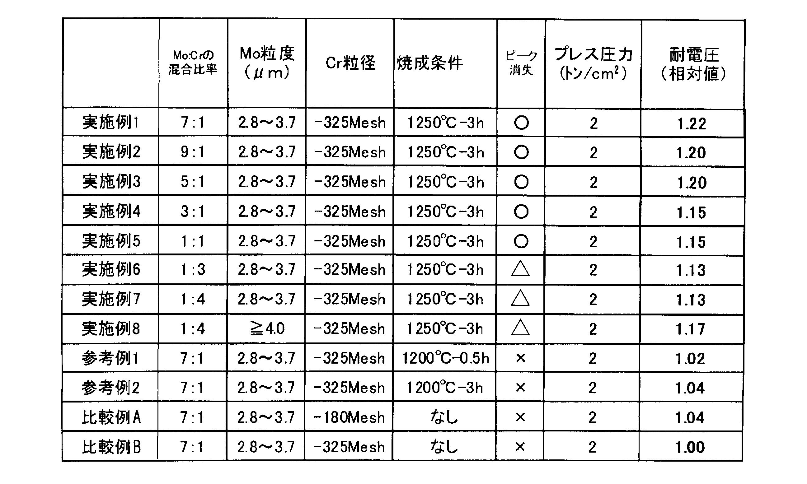
表1に示した実施例1-8から明らかなように、実施例1-8の電極材料は、比較例A,Bと比較して耐電圧性能に優れた電極材料である。また、電極材料に含有される耐熱元素の割合が増加するにしたがって、電極材料の耐電圧性能が向上していることがわかる。すなわち、実施例1-8の電極材料は、耐熱元素粉末とCr粉末とを混合する混合工程と、耐熱元素粉末とCr粉末の混合物を仮焼結する仮焼結工程と、仮焼結体を粉砕する粉砕工程と、仮焼結体を粉砕した粉末を焼結する本焼結工程と、本焼結工程で得られる焼結体(スケルトン)にCuを溶浸させるCu溶浸工程とを行うことで、耐熱元素とCrが相互に固溶拡散した粒子を微細化して均一に分散させ、高導電体成分であるCu部分も微細均一分散した組成となるように合金組成を制御することができる。
[絶縁回復性能の評価]
実施例1の電極材料を電極接点材(固定電極及び可動電極)として真空インタラプタ(以後、実施例1の真空インタラプタと称する)を構成し、真空インタラプタの絶縁回復性能の評価を行った。表2に電極接点材の条件及び操作器の条件を示す。また、図7に、実施例1の真空インタラプタ及び比較例1,2の真空インタラプタの絶縁回復特性の特性図を示す。
実施例1の電極材料を電極接点材(固定電極及び可動電極)として真空インタラプタ(以後、実施例1の真空インタラプタと称する)を構成し、真空インタラプタの絶縁回復性能の評価を行った。表2に電極接点材の条件及び操作器の条件を示す。また、図7に、実施例1の真空インタラプタ及び比較例1,2の真空インタラプタの絶縁回復特性の特性図を示す。
なお、比較例1の真空インタラプタは、従来の真空インタラプタであり、CuCr電極材料を固定電極及び可動電極に備え、遮断速度が3.0m/s、遮断時ギャップ長が60mmの真空インタラプタである。CuCr電極材料は、実施例1の電極材料と同じ材料(Cr粉末)を用いて作製された電極材料であり、Crを焼結した後、Cuを溶浸して作製した電極材料である。また、比較例2の真空インタラプタは、比較例1の真空インタラプタと同じCuCr電極材料を備えた真空インタラプタであって、遮断速度及び遮断時ギャップ長を、実施例1の真空インタラプタと同じ条件にした真空インタラプタである。
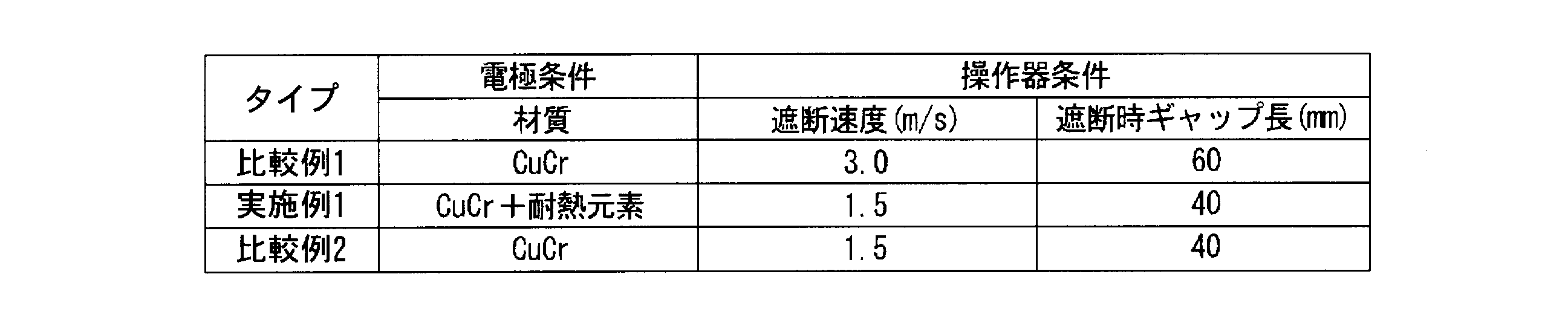
図7に示すように、実施例1の真空インタラプタは、比較例1の真空インタラプタと同程度の絶縁回復特性を有している。つまり、表2に示すように、実施例1の真空インタラプタは、比較例1の真空インタラプタと比較して遮断速度を50%低減し、遮断時のギャップ長を33%低減した場合において、従来技術に係る真空インタラプタと同じ程度の絶縁回復特性を有する真空インタラプタである。一方で、比較例1の真空インタラプタと比較例2の真空インタラプタとの比較から明らかなように、CuCr電極材料を電極接点として用い、遮断速度を遅くし、遮断時ギャップ長を短くすると、真空インタラプタの絶縁回復特性が低下する。なお、実施例2-8の電極材料も実施例1の電極材料と同様に、遮断速度を低減し、遮断時のギャップ長を低減した場合において、従来技術に係る真空インタラプタと同じ程度の絶縁回復性能を有する真空インタラプタを構成することができた。
以上のような、本発明の実施形態に係る真空遮断器によれば、電極材料の耐電圧性能を向上させることで、遮断時の絶縁回復性能が向上し、真空遮断器の遮断速度を低減し、遮断時ギャップ長を低減することができる。その結果、真空遮断器の操作力を低減できるとともに、ストロークに関連した機構の小型化、機器の縮小化、部品点数が低減され、真空遮断器の信頼性が向上する。
また、固定電極(または可動電極)と主シールドとの間のギャップを狭めることができるため、真空インタラプタの構造を小さくすることが可能となる。その結果、真空インタラプタ及び真空遮断器を小型化することができ、真空遮断器の製造コストが低減する。
つまり、本発明の実施形態に係る真空遮断器は、電極材料の耐電圧性能を向上させることにより、真空遮断器の遮断速度または遮断時のギャップ長を低減するものである。
本発明の実施形態に係る真空遮断器に設けられる電極材料は、耐熱元素とCrが相互に固溶拡散した微細粒子(耐熱元素とCrの固溶体粒子)が均一に分散した組織を有する電極材料である。この微細粒子の平均粒子径は、原料であるMo粉末の平均粒子径やCr粉末の平均粒子径に応じて変化することとなるが、電極材料に分散される微細粒子の平均粒子径を、フルマンの式を用いて求めた平均粒子径が20μm以下、より好ましくは15μm以下の大きさとなるように制御することで、電極材料の電流遮断性能及び耐電圧性能が向上する。
また、MoCr粉末を仮焼結・粉砕後に測定したMoCr粉末の粒径と、フルマンの式によりCu溶浸工程後の電極材料にて測定されたMoCr粉末の平均粒子径とを比較すると、Cu溶浸工程において、MoCr粒子の微細化がさらに進行していることが確認できる。具体的には、粉砕後のMoCr粉末は、d50=30μmであったのに対して、フルマンの式によりCu溶浸工程後の電極材料におけるMoCr粉末の平均粒子径は、10μm以下である。このことより、MoCr粉末を、30μm以下の粒子が体積相対粒子量で50%以上とすることで、耐電圧性能及び電流遮断性能に優れた電極材料を得ることができる。このように、Cu溶浸工程において、耐熱元素とCrの固溶体粒子をさらに微細化することができるので、実施例6~8の電極材料のように、耐熱元素とCrの固溶体粉末のXRD測定においてCr元素のピークがわずかに残っている場合でも、耐電圧性能及び電流遮断性能に優れた電極材料を得ることができる。
また、耐熱元素とCrが相互に固溶拡散した微細粒子(耐熱元素とCrの固溶体粒子)の重心間距離の平均値と標準偏差から求めた分散状態指数CVを、2.0以下、望ましくは、1.0以下となるように制御することで、電極材料の電流遮断性能及び耐電圧性能が向上する。
また、電極材料に対する耐熱元素の含有量を多くすることで、電極材料の耐電圧性能及び電流遮断性能が向上する。ただし、電極材料に耐熱元素のみ含有させた場合(電極材料にCrを含有させない場合)には、Cuの溶浸が困難となるおそれがある。よって、固溶体粉末における耐熱元素とCr元素の割合は、重量比率で耐熱元素1に対してCrが4以下、より好ましくは耐熱元素1に対してCrが1/3以下とすることで、電極材料の耐電圧性能が向上する。
また、MoCr焼結体に対してHIP処理を行った後に、MoCr焼結体にCuを溶浸させることで、電極材料に含有される耐熱元素の含有量がさらに多くなり、電極材料の耐電圧性能が向上する。
また、耐熱元素(Mo等)の平均粒子径の大きさは、耐熱元素とCrの固溶体粉末の粒子径を決定する一つの要因となり得る。すなわち、Cr粒子が耐熱元素粒子によって微細化され、拡散機構によって耐熱元素粒子にCrが拡散して耐熱元素とCrとが固溶体組織を形成することから、耐熱元素の粒径は、仮焼結によって大きくなる。また、仮焼結によって大きくなる度合いは、Crの混合割合にも依存する。そのため、耐熱元素粉末の平均粒子径を、例えば、2~20μm、より好ましくは、2~10μmとすることで、耐電圧性能及び電流遮断性能に優れた電極材料を形成するための耐熱元素とCrの固溶体粉末を得ることができる。
また、溶浸法で製造された電極材料は、充填率が95%以上となり、電流遮断時や電流開閉時のアークによる接点表面の表面荒れが少ない。すなわち、空孔の存在による電極材料表面の微細な凹凸がなく、電極材料の耐電圧性能が向上する。また、多孔質体の空隙部にCuを充填することで、電極材料の機械的強度が向上し、焼結法により製造される電極材料よりも高硬度となり、電極材料の耐電圧性能が向上する。
また、耐熱元素とCrが相互に固溶拡散した粒子を微細化して均一に分散し、高導電体成分であるCu部分も微細均一分散した組成を有するように電極材料の組成を制御することで、電極材料の耐電圧性能が向上する。
なお、本発明の実施形態の説明は、特定の望ましい実施例を例として説明したが、本発明は、実施例に限定されるものではなく、発明の特徴を損なわない範囲で、適宜設計変更が可能であり、設計変更された形態も本発明の技術範囲に属する。
例えば、本発明の実施形態の説明において、仮焼結温度は、1250℃-3時間の条件であるが、本発明の仮焼結温度は、1250℃以上且つCrの融点以下、より好ましくは1250℃~1500℃の範囲で行うことで、MoとCrの相互拡散が充分に進行し、且つその後の粉砕機を用いたMoCr固溶体の粉砕が比較的容易に行え、さらには耐電圧性能及び電流遮断性能に優れた電極材料を製造することができる。また、仮焼結時間は、仮焼結温度によって異なるものであり、例えば、1250℃では、3時間の仮焼結を行っているが、1500℃では、0.5時間の仮焼結で十分である。
また、MoCr固溶体粉末は、実施形態に記載されている製造方法により製造されたものに限定されず、公知の製造方法(例えば、ジェットミル法、アトマイズ法)で製造されたMoCr固溶体粉末を用いてもよい。
また、本発明の真空遮断器に設けられる電極材料は、耐熱元素とCrが相互に固溶拡散した微細粒子(耐熱元素とCrの固溶体粒子)を、均一に分散させたものであれば、フルマンの式を用いて求めた平均粒子径20μm以下(より好ましくは15μm以下)であって、微細粒子の重心間距離の平均値と標準偏差から求めた分散状態指数CVが2.0以下(より好ましくは、CVが1.0以下)であれば、実施形態の製造方法に限定されるものではなく、例えば、CuとCr等を所定の組成比で溶解する溶解法で製造したものであってもよい。
また、実施形態では、接地タンクに真空インタラプタを収納した真空遮断器を例示したが、真空インタラプタは、箱形や管路型のGIS(ガス絶縁開閉装置)に搭載することもできる。また、真空インタラプタに設けられる電極(接点)は、調相設備開閉能力及び遮断電流開閉能力を有する真空遮断器(VCB)の他、調相設備開閉能力のみを有する真空開閉器(VS)、さらには、調相用以外にも適用することができる。
Claims (2)
- 絶縁性ガスが封入された容器に真空インタラプタを収納した真空遮断器であって、
前記真空インタラプタは、絶縁筒と当該絶縁筒の両端部を封止する封着金具とで構成された真空容器と、該真空容器内に収納され、且つ導通軸に固着された互いに接離可能な一対の接点を有し、
前記接点のうち少なくとも一方の接点が、Cu相と、Mo、W、Ta、Nb、V、Zrのいずれかの耐熱元素とCrの固溶体を含有する固溶体粒子相と、を有する電極材料であり、
前記電極材料は、当該電極材料に対して重量比で、
Cuを20~70%、
Crを1.5~64%、
耐熱元素を6~76%、含有し、
前記電極材料に含まれる固溶体粒子の平均粒子径が20μm以下である、真空遮断器。 - 前記電極材料中の前記固溶体粒子の分散状態指数は2.0以下である、請求項1に記載の真空遮断器。
Priority Applications (2)
| Application Number | Priority Date | Filing Date | Title |
|---|---|---|---|
| EP16841570.1A EP3346480B1 (en) | 2015-09-03 | 2016-08-23 | Vacuum circuit breaker |
| US15/757,108 US10262819B2 (en) | 2015-09-03 | 2016-08-23 | Vacuum circuit breaker |
Applications Claiming Priority (2)
| Application Number | Priority Date | Filing Date | Title |
|---|---|---|---|
| JP2015173407A JP6075423B1 (ja) | 2015-09-03 | 2015-09-03 | 真空遮断器 |
| JP2015-173407 | 2015-09-03 |
Publications (1)
| Publication Number | Publication Date |
|---|---|
| WO2017038538A1 true WO2017038538A1 (ja) | 2017-03-09 |
Family
ID=57981488
Family Applications (1)
| Application Number | Title | Priority Date | Filing Date |
|---|---|---|---|
| PCT/JP2016/074430 Ceased WO2017038538A1 (ja) | 2015-09-03 | 2016-08-23 | 真空遮断器 |
Country Status (4)
| Country | Link |
|---|---|
| US (1) | US10262819B2 (ja) |
| EP (1) | EP3346480B1 (ja) |
| JP (1) | JP6075423B1 (ja) |
| WO (1) | WO2017038538A1 (ja) |
Cited By (1)
| Publication number | Priority date | Publication date | Assignee | Title |
|---|---|---|---|---|
| WO2022138607A1 (ja) * | 2020-12-23 | 2022-06-30 | 三菱電機株式会社 | 真空遮断器 |
Families Citing this family (8)
| Publication number | Priority date | Publication date | Assignee | Title |
|---|---|---|---|---|
| JP6075423B1 (ja) | 2015-09-03 | 2017-02-08 | 株式会社明電舎 | 真空遮断器 |
| JP6778129B2 (ja) * | 2017-02-21 | 2020-10-28 | 株式会社日立産機システム | 鉄道車両用開閉器ユニット |
| JP6752395B1 (ja) * | 2020-01-10 | 2020-09-09 | 三菱電機株式会社 | 真空遮断器 |
| WO2023283110A1 (en) * | 2021-07-09 | 2023-01-12 | S&C Electric Company | Rotary diaphragm in vacuum interrupter switch |
| WO2023286112A1 (ja) * | 2021-07-12 | 2023-01-19 | 三菱電機株式会社 | 真空遮断器 |
| JP7090825B1 (ja) * | 2021-09-28 | 2022-06-24 | 三菱電機株式会社 | タンク型遮断器 |
| US20240347294A1 (en) * | 2021-12-20 | 2024-10-17 | Mitsubishi Electric Corporation | Vacuum circuit breaker |
| US12033820B2 (en) * | 2022-07-07 | 2024-07-09 | Southern States, Llc | Modular vacuum circuit interrupter |
Citations (5)
| Publication number | Priority date | Publication date | Assignee | Title |
|---|---|---|---|---|
| JPS59119625A (ja) * | 1982-12-24 | 1984-07-10 | 株式会社明電舎 | 真空インタラプタの電極 |
| JPH0474924A (ja) * | 1990-07-14 | 1992-03-10 | Matsushita Electric Works Ltd | 材料組織評価方法 |
| JPH11232971A (ja) * | 1998-02-12 | 1999-08-27 | Hitachi Ltd | 真空遮断器及びそれに用いる真空バルブと電気接点並びに製造方法 |
| JP2012007203A (ja) * | 2010-06-24 | 2012-01-12 | Japan Ae Power Systems Corp | 真空遮断器用電極材料の製造方法及び真空遮断器用電極材料 |
| JP2014067512A (ja) * | 2012-09-25 | 2014-04-17 | Mitsubishi Electric Corp | 真空遮断装置 |
Family Cites Families (24)
| Publication number | Priority date | Publication date | Assignee | Title |
|---|---|---|---|---|
| JPH0715127B2 (ja) * | 1987-01-26 | 1995-02-22 | 株式会社明電舎 | 電極材料の製造方法 |
| JPH04334832A (ja) * | 1991-05-09 | 1992-11-20 | Meidensha Corp | 電極材料の製造方法 |
| US5461214A (en) * | 1992-06-15 | 1995-10-24 | Thermtec, Inc. | High performance horizontal diffusion furnace system |
| US5697150A (en) * | 1993-07-14 | 1997-12-16 | Hitachi, Ltd. | Method forming an electric contact in a vacuum circuit breaker |
| US5852266A (en) * | 1993-07-14 | 1998-12-22 | Hitachi, Ltd. | Vacuum circuit breaker as well as vacuum valve and electric contact used in same |
| TW293130B (ja) * | 1994-03-10 | 1996-12-11 | Mitsubishi Electric Corp | |
| JP2941682B2 (ja) * | 1994-05-12 | 1999-08-25 | 株式会社東芝 | 真空バルブ及びその製造方法 |
| DE19903619C1 (de) * | 1999-01-29 | 2000-06-08 | Louis Renner Gmbh | Pulvermetallurgisch hergestellter Verbundwerkstoff und Verfahren zu dessen Herstellung sowie dessen Verwendung |
| KR100400356B1 (ko) * | 2000-12-06 | 2003-10-04 | 한국과학기술연구원 | 진공개폐기용 구리-크롬계 접점 소재의 조직 제어 방법 |
| JP2002245907A (ja) * | 2001-02-14 | 2002-08-30 | Hitachi Ltd | 真空バルブ用電極とその製法及び真空バルブ並びに真空遮断器と真空バルブ電極用電気接点 |
| JP4709062B2 (ja) | 2006-05-11 | 2011-06-22 | 株式会社日本Aeパワーシステムズ | タンク形真空遮断器 |
| US20080194441A1 (en) * | 2007-02-09 | 2008-08-14 | Fujifilm Corporation | Grease composition, viscous agent, and mechanical element |
| AT509407A1 (de) * | 2008-03-05 | 2011-08-15 | Moeller Gebaeudeautomation Gmbh | Schaltgerät |
| EP2586882B1 (en) | 2010-06-24 | 2016-08-31 | Meidensha Corporation | Method for producing electrode material for vacuum circuit breaker, electrode material for vacuum circuit breaker and electrode for vacuum circuit breaker |
| JP5199498B2 (ja) * | 2011-04-27 | 2013-05-15 | 株式会社日立製作所 | 電気接点用グリース及び摺動通電構造、電力用開閉機器、真空遮断器、真空絶縁スイッチギヤ、並びに真空絶縁スイッチギヤの組立方法 |
| JP6068830B2 (ja) | 2011-05-12 | 2017-01-25 | 株式会社タンガロイ | 超硬合金および被覆超硬合金 |
| EP2682973B1 (en) * | 2012-07-02 | 2017-04-05 | ABB Schweiz AG | Circuit-breaker pole part with a heat transfer shield |
| CN104969323B (zh) * | 2013-02-07 | 2017-10-20 | 三菱电机株式会社 | 消弧用绝缘材料成形体、使用了其的气体断路器 |
| EP2838096B1 (en) * | 2013-08-16 | 2017-07-19 | General Electric Company | Electrical contact system |
| IN2013CH05861A (ja) * | 2013-12-16 | 2015-06-19 | Gen Electric | |
| JP5862695B2 (ja) * | 2014-01-23 | 2016-02-16 | 株式会社明電舎 | 電極材料の製造方法 |
| EP3106534B1 (en) | 2014-03-04 | 2019-08-07 | Meidensha Corporation | Alloy comprising copper and chromium |
| DE112015002850T5 (de) * | 2014-06-19 | 2017-03-09 | Panasonic Intellectual Property Management Co., Ltd. | Kontaktvorrichtung, elektromagnetisches Relais, das sie verwendet, und Verfahren zum Herstellen der Kontaktvorrichtung |
| JP6075423B1 (ja) | 2015-09-03 | 2017-02-08 | 株式会社明電舎 | 真空遮断器 |
-
2015
- 2015-09-03 JP JP2015173407A patent/JP6075423B1/ja active Active
-
2016
- 2016-08-23 WO PCT/JP2016/074430 patent/WO2017038538A1/ja not_active Ceased
- 2016-08-23 US US15/757,108 patent/US10262819B2/en active Active
- 2016-08-23 EP EP16841570.1A patent/EP3346480B1/en active Active
Patent Citations (5)
| Publication number | Priority date | Publication date | Assignee | Title |
|---|---|---|---|---|
| JPS59119625A (ja) * | 1982-12-24 | 1984-07-10 | 株式会社明電舎 | 真空インタラプタの電極 |
| JPH0474924A (ja) * | 1990-07-14 | 1992-03-10 | Matsushita Electric Works Ltd | 材料組織評価方法 |
| JPH11232971A (ja) * | 1998-02-12 | 1999-08-27 | Hitachi Ltd | 真空遮断器及びそれに用いる真空バルブと電気接点並びに製造方法 |
| JP2012007203A (ja) * | 2010-06-24 | 2012-01-12 | Japan Ae Power Systems Corp | 真空遮断器用電極材料の製造方法及び真空遮断器用電極材料 |
| JP2014067512A (ja) * | 2012-09-25 | 2014-04-17 | Mitsubishi Electric Corp | 真空遮断装置 |
Non-Patent Citations (1)
| Title |
|---|
| See also references of EP3346480A4 * |
Cited By (4)
| Publication number | Priority date | Publication date | Assignee | Title |
|---|---|---|---|---|
| WO2022138607A1 (ja) * | 2020-12-23 | 2022-06-30 | 三菱電機株式会社 | 真空遮断器 |
| JPWO2022138607A1 (ja) * | 2020-12-23 | 2022-06-30 | ||
| JP7226650B2 (ja) | 2020-12-23 | 2023-02-21 | 三菱電機株式会社 | 真空遮断器 |
| US12381051B2 (en) | 2020-12-23 | 2025-08-05 | Mitsubishi Electric Corporation | Vacuum circuit breaker |
Also Published As
| Publication number | Publication date |
|---|---|
| EP3346480A1 (en) | 2018-07-11 |
| JP2017050191A (ja) | 2017-03-09 |
| EP3346480B1 (en) | 2019-12-25 |
| US10262819B2 (en) | 2019-04-16 |
| US20180247780A1 (en) | 2018-08-30 |
| JP6075423B1 (ja) | 2017-02-08 |
| EP3346480A4 (en) | 2019-03-20 |
Similar Documents
| Publication | Publication Date | Title |
|---|---|---|
| JP6075423B1 (ja) | 真空遮断器 | |
| JP5904308B2 (ja) | 電極材料の製造方法 | |
| JP5880789B1 (ja) | 固溶体粒子を成形した成形体にCuを溶浸した複合金属 | |
| JP5862695B2 (ja) | 電極材料の製造方法 | |
| US10614969B2 (en) | Method for manufacturing electrode material and electrode material | |
| JP5861807B1 (ja) | 電極材料の製造方法 | |
| JP6311325B2 (ja) | 電極材料及び電極材料の製造方法 | |
| US10058923B2 (en) | Method for manufacturing electrode material and electrode material | |
| JP6398415B2 (ja) | 電極材料の製造方法 | |
| EP3290535A1 (en) | Method for producing electrode material, and electrode material | |
| JP6398530B2 (ja) | 電極材料の製造方法 | |
| WO2017026509A1 (ja) | 電極材料及び電極材料の製造方法 | |
| JP6507830B2 (ja) | 電極材料の製造方法及び電極材料 |
Legal Events
| Date | Code | Title | Description |
|---|---|---|---|
| 121 | Ep: the epo has been informed by wipo that ep was designated in this application |
Ref document number: 16841570 Country of ref document: EP Kind code of ref document: A1 |
|
| WWE | Wipo information: entry into national phase |
Ref document number: 15757108 Country of ref document: US |
|
| NENP | Non-entry into the national phase |
Ref country code: DE |
|
| WWE | Wipo information: entry into national phase |
Ref document number: 2016841570 Country of ref document: EP |