WO2017046932A1 - Transistor à couches minces et procédé de fabrication de transistor à couches minces - Google Patents
Transistor à couches minces et procédé de fabrication de transistor à couches minces Download PDFInfo
- Publication number
- WO2017046932A1 WO2017046932A1 PCT/JP2015/076592 JP2015076592W WO2017046932A1 WO 2017046932 A1 WO2017046932 A1 WO 2017046932A1 JP 2015076592 W JP2015076592 W JP 2015076592W WO 2017046932 A1 WO2017046932 A1 WO 2017046932A1
- Authority
- WO
- WIPO (PCT)
- Prior art keywords
- silicon layer
- polycrystalline
- silicon
- thin film
- film transistor
- Prior art date
- Legal status (The legal status is an assumption and is not a legal conclusion. Google has not performed a legal analysis and makes no representation as to the accuracy of the status listed.)
- Ceased
Links
Images




Classifications
-
- H—ELECTRICITY
- H10—SEMICONDUCTOR DEVICES; ELECTRIC SOLID-STATE DEVICES NOT OTHERWISE PROVIDED FOR
- H10D—INORGANIC ELECTRIC SEMICONDUCTOR DEVICES
- H10D30/00—Field-effect transistors [FET]
- H10D30/01—Manufacture or treatment
- H10D30/021—Manufacture or treatment of FETs having insulated gates [IGFET]
- H10D30/031—Manufacture or treatment of FETs having insulated gates [IGFET] of thin-film transistors [TFT]
- H10D30/0321—Manufacture or treatment of FETs having insulated gates [IGFET] of thin-film transistors [TFT] comprising silicon, e.g. amorphous silicon or polysilicon
-
- H—ELECTRICITY
- H10—SEMICONDUCTOR DEVICES; ELECTRIC SOLID-STATE DEVICES NOT OTHERWISE PROVIDED FOR
- H10D—INORGANIC ELECTRIC SEMICONDUCTOR DEVICES
- H10D30/00—Field-effect transistors [FET]
- H10D30/01—Manufacture or treatment
- H10D30/021—Manufacture or treatment of FETs having insulated gates [IGFET]
- H10D30/031—Manufacture or treatment of FETs having insulated gates [IGFET] of thin-film transistors [TFT]
- H10D30/0312—Manufacture or treatment of FETs having insulated gates [IGFET] of thin-film transistors [TFT] characterised by the gate electrodes
- H10D30/0316—Manufacture or treatment of FETs having insulated gates [IGFET] of thin-film transistors [TFT] characterised by the gate electrodes of lateral bottom-gate TFTs comprising only a single gate
-
- H—ELECTRICITY
- H10—SEMICONDUCTOR DEVICES; ELECTRIC SOLID-STATE DEVICES NOT OTHERWISE PROVIDED FOR
- H10D—INORGANIC ELECTRIC SEMICONDUCTOR DEVICES
- H10D30/00—Field-effect transistors [FET]
- H10D30/60—Insulated-gate field-effect transistors [IGFET]
- H10D30/67—Thin-film transistors [TFT]
-
- H—ELECTRICITY
- H10—SEMICONDUCTOR DEVICES; ELECTRIC SOLID-STATE DEVICES NOT OTHERWISE PROVIDED FOR
- H10D—INORGANIC ELECTRIC SEMICONDUCTOR DEVICES
- H10D30/00—Field-effect transistors [FET]
- H10D30/60—Insulated-gate field-effect transistors [IGFET]
- H10D30/67—Thin-film transistors [TFT]
- H10D30/6704—Thin-film transistors [TFT] having supplementary regions or layers in the thin films or in the insulated bulk substrates for controlling properties of the device
- H10D30/6706—Thin-film transistors [TFT] having supplementary regions or layers in the thin films or in the insulated bulk substrates for controlling properties of the device for preventing leakage current
-
- H—ELECTRICITY
- H10—SEMICONDUCTOR DEVICES; ELECTRIC SOLID-STATE DEVICES NOT OTHERWISE PROVIDED FOR
- H10D—INORGANIC ELECTRIC SEMICONDUCTOR DEVICES
- H10D30/00—Field-effect transistors [FET]
- H10D30/60—Insulated-gate field-effect transistors [IGFET]
- H10D30/67—Thin-film transistors [TFT]
- H10D30/6729—Thin-film transistors [TFT] characterised by the electrodes
- H10D30/673—Thin-film transistors [TFT] characterised by the electrodes characterised by the shapes, relative sizes or dispositions of the gate electrodes
- H10D30/6732—Bottom-gate only TFTs
-
- H—ELECTRICITY
- H10—SEMICONDUCTOR DEVICES; ELECTRIC SOLID-STATE DEVICES NOT OTHERWISE PROVIDED FOR
- H10D—INORGANIC ELECTRIC SEMICONDUCTOR DEVICES
- H10D30/00—Field-effect transistors [FET]
- H10D30/60—Insulated-gate field-effect transistors [IGFET]
- H10D30/67—Thin-film transistors [TFT]
- H10D30/674—Thin-film transistors [TFT] characterised by the active materials
- H10D30/6741—Group IV materials, e.g. germanium or silicon carbide
- H10D30/6743—Silicon
- H10D30/6745—Polycrystalline or microcrystalline silicon
-
- H—ELECTRICITY
- H10—SEMICONDUCTOR DEVICES; ELECTRIC SOLID-STATE DEVICES NOT OTHERWISE PROVIDED FOR
- H10D—INORGANIC ELECTRIC SEMICONDUCTOR DEVICES
- H10D30/00—Field-effect transistors [FET]
- H10D30/60—Insulated-gate field-effect transistors [IGFET]
- H10D30/67—Thin-film transistors [TFT]
- H10D30/674—Thin-film transistors [TFT] characterised by the active materials
- H10D30/6741—Group IV materials, e.g. germanium or silicon carbide
- H10D30/6743—Silicon
- H10D30/6746—Amorphous silicon
-
- H—ELECTRICITY
- H10—SEMICONDUCTOR DEVICES; ELECTRIC SOLID-STATE DEVICES NOT OTHERWISE PROVIDED FOR
- H10D—INORGANIC ELECTRIC SEMICONDUCTOR DEVICES
- H10D30/00—Field-effect transistors [FET]
- H10D30/60—Insulated-gate field-effect transistors [IGFET]
- H10D30/67—Thin-film transistors [TFT]
- H10D30/6757—Thin-film transistors [TFT] characterised by the structure of the channel, e.g. transverse or longitudinal shape or doping profile
-
- H—ELECTRICITY
- H10—SEMICONDUCTOR DEVICES; ELECTRIC SOLID-STATE DEVICES NOT OTHERWISE PROVIDED FOR
- H10P—GENERIC PROCESSES OR APPARATUS FOR THE MANUFACTURE OR TREATMENT OF DEVICES COVERED BY CLASS H10
- H10P14/00—Formation of materials, e.g. in the shape of layers or pillars
- H10P14/20—Formation of materials, e.g. in the shape of layers or pillars of semiconductor materials
- H10P14/34—Deposited materials, e.g. layers
- H10P14/3402—Deposited materials, e.g. layers characterised by the chemical composition
- H10P14/3404—Deposited materials, e.g. layers characterised by the chemical composition being Group IVA materials
- H10P14/3411—Silicon, silicon germanium or germanium
-
- H—ELECTRICITY
- H10—SEMICONDUCTOR DEVICES; ELECTRIC SOLID-STATE DEVICES NOT OTHERWISE PROVIDED FOR
- H10P—GENERIC PROCESSES OR APPARATUS FOR THE MANUFACTURE OR TREATMENT OF DEVICES COVERED BY CLASS H10
- H10P14/00—Formation of materials, e.g. in the shape of layers or pillars
- H10P14/20—Formation of materials, e.g. in the shape of layers or pillars of semiconductor materials
- H10P14/34—Deposited materials, e.g. layers
- H10P14/3451—Structure
- H10P14/3452—Microstructure
- H10P14/3454—Amorphous
-
- H—ELECTRICITY
- H10—SEMICONDUCTOR DEVICES; ELECTRIC SOLID-STATE DEVICES NOT OTHERWISE PROVIDED FOR
- H10P—GENERIC PROCESSES OR APPARATUS FOR THE MANUFACTURE OR TREATMENT OF DEVICES COVERED BY CLASS H10
- H10P14/00—Formation of materials, e.g. in the shape of layers or pillars
- H10P14/20—Formation of materials, e.g. in the shape of layers or pillars of semiconductor materials
- H10P14/38—Formation of materials, e.g. in the shape of layers or pillars of semiconductor materials characterised by treatments done after the formation of the materials
- H10P14/3802—Crystallisation or recrystallisation of non-monocrystalline semiconductor materials, e.g. regrowth
- H10P14/3808—Crystallisation or recrystallisation of non-monocrystalline semiconductor materials, e.g. regrowth using laser beams
- H10P14/381—Beam shaping, e.g. using a mask
-
- G—PHYSICS
- G02—OPTICS
- G02F—OPTICAL DEVICES OR ARRANGEMENTS FOR THE CONTROL OF LIGHT BY MODIFICATION OF THE OPTICAL PROPERTIES OF THE MEDIA OF THE ELEMENTS INVOLVED THEREIN; NON-LINEAR OPTICS; FREQUENCY-CHANGING OF LIGHT; OPTICAL LOGIC ELEMENTS; OPTICAL ANALOGUE/DIGITAL CONVERTERS
- G02F1/00—Devices or arrangements for the control of the intensity, colour, phase, polarisation or direction of light arriving from an independent light source, e.g. switching, gating or modulating; Non-linear optics
- G02F1/01—Devices or arrangements for the control of the intensity, colour, phase, polarisation or direction of light arriving from an independent light source, e.g. switching, gating or modulating; Non-linear optics for the control of the intensity, phase, polarisation or colour
- G02F1/13—Devices or arrangements for the control of the intensity, colour, phase, polarisation or direction of light arriving from an independent light source, e.g. switching, gating or modulating; Non-linear optics for the control of the intensity, phase, polarisation or colour based on liquid crystals, e.g. single liquid crystal display cells
- G02F1/133—Constructional arrangements; Operation of liquid crystal cells; Circuit arrangements
- G02F1/136—Liquid crystal cells structurally associated with a semi-conducting layer or substrate, e.g. cells forming part of an integrated circuit
- G02F1/1362—Active matrix addressed cells
- G02F1/1368—Active matrix addressed cells in which the switching element is a three-electrode device
-
- G—PHYSICS
- G02—OPTICS
- G02F—OPTICAL DEVICES OR ARRANGEMENTS FOR THE CONTROL OF LIGHT BY MODIFICATION OF THE OPTICAL PROPERTIES OF THE MEDIA OF THE ELEMENTS INVOLVED THEREIN; NON-LINEAR OPTICS; FREQUENCY-CHANGING OF LIGHT; OPTICAL LOGIC ELEMENTS; OPTICAL ANALOGUE/DIGITAL CONVERTERS
- G02F2202/00—Materials and properties
- G02F2202/10—Materials and properties semiconductor
- G02F2202/103—Materials and properties semiconductor a-Si
-
- G—PHYSICS
- G02—OPTICS
- G02F—OPTICAL DEVICES OR ARRANGEMENTS FOR THE CONTROL OF LIGHT BY MODIFICATION OF THE OPTICAL PROPERTIES OF THE MEDIA OF THE ELEMENTS INVOLVED THEREIN; NON-LINEAR OPTICS; FREQUENCY-CHANGING OF LIGHT; OPTICAL LOGIC ELEMENTS; OPTICAL ANALOGUE/DIGITAL CONVERTERS
- G02F2202/00—Materials and properties
- G02F2202/10—Materials and properties semiconductor
- G02F2202/104—Materials and properties semiconductor poly-Si
-
- H—ELECTRICITY
- H10—SEMICONDUCTOR DEVICES; ELECTRIC SOLID-STATE DEVICES NOT OTHERWISE PROVIDED FOR
- H10D—INORGANIC ELECTRIC SEMICONDUCTOR DEVICES
- H10D86/00—Integrated devices formed in or on insulating or conducting substrates, e.g. formed in silicon-on-insulator [SOI] substrates or on stainless steel or glass substrates
- H10D86/01—Manufacture or treatment
- H10D86/021—Manufacture or treatment of multiple TFTs
- H10D86/0221—Manufacture or treatment of multiple TFTs comprising manufacture, treatment or patterning of TFT semiconductor bodies
- H10D86/0223—Manufacture or treatment of multiple TFTs comprising manufacture, treatment or patterning of TFT semiconductor bodies comprising crystallisation of amorphous, microcrystalline or polycrystalline semiconductor materials
- H10D86/0229—Manufacture or treatment of multiple TFTs comprising manufacture, treatment or patterning of TFT semiconductor bodies comprising crystallisation of amorphous, microcrystalline or polycrystalline semiconductor materials characterised by control of the annealing or irradiation parameters
-
- H—ELECTRICITY
- H10—SEMICONDUCTOR DEVICES; ELECTRIC SOLID-STATE DEVICES NOT OTHERWISE PROVIDED FOR
- H10D—INORGANIC ELECTRIC SEMICONDUCTOR DEVICES
- H10D86/00—Integrated devices formed in or on insulating or conducting substrates, e.g. formed in silicon-on-insulator [SOI] substrates or on stainless steel or glass substrates
- H10D86/40—Integrated devices formed in or on insulating or conducting substrates, e.g. formed in silicon-on-insulator [SOI] substrates or on stainless steel or glass substrates characterised by multiple TFTs
- H10D86/421—Integrated devices formed in or on insulating or conducting substrates, e.g. formed in silicon-on-insulator [SOI] substrates or on stainless steel or glass substrates characterised by multiple TFTs having a particular composition, shape or crystalline structure of the active layer
- H10D86/425—Integrated devices formed in or on insulating or conducting substrates, e.g. formed in silicon-on-insulator [SOI] substrates or on stainless steel or glass substrates characterised by multiple TFTs having a particular composition, shape or crystalline structure of the active layer having different crystal properties in different TFTs or within an individual TFT
-
- H—ELECTRICITY
- H10—SEMICONDUCTOR DEVICES; ELECTRIC SOLID-STATE DEVICES NOT OTHERWISE PROVIDED FOR
- H10D—INORGANIC ELECTRIC SEMICONDUCTOR DEVICES
- H10D86/00—Integrated devices formed in or on insulating or conducting substrates, e.g. formed in silicon-on-insulator [SOI] substrates or on stainless steel or glass substrates
- H10D86/40—Integrated devices formed in or on insulating or conducting substrates, e.g. formed in silicon-on-insulator [SOI] substrates or on stainless steel or glass substrates characterised by multiple TFTs
- H10D86/60—Integrated devices formed in or on insulating or conducting substrates, e.g. formed in silicon-on-insulator [SOI] substrates or on stainless steel or glass substrates characterised by multiple TFTs wherein the TFTs are in active matrices
Definitions
- the amorphous silicon layer is partially irradiated with laser light to change part of the amorphous silicon layer to polycrystalline silicon.
- Technology to make it develop.
- the leakage current can be reduced compared to the case where the entire amorphous silicon layer is changed to polycrystalline silicon.
- the thin film transistor according to the present invention includes a part of an end of the silicon layer at a position where the source electrode and the drain electrode are projected onto the silicon layer, and the amorphous part is provided in the part. It is characterized by being.
- a part of the position where the source electrode and the drain electrode are projected onto the silicon layer is a part of the end of the silicon layer, and this part is an amorphous part.
- the current flowing between the source electrode and the drain electrode is affected by the amorphous part.
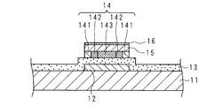
- FIG. 1 is a schematic cross-sectional view of a main part of the TFT according to the first embodiment.
- a gate electrode 12 is formed on the surface of an insulating substrate 11 such as a glass substrate, and a gate insulating film 13 is formed on the substrate 11 so as to cover the gate electrode 12.
- the gate insulating film 13 is, for example, a silicon nitride layer.
- a silicon layer 14 is formed above the gate electrode 12 in the surface of the gate insulating film 13.
- the silicon layer 14 includes an amorphous portion 141 made of amorphous silicon, a first polycrystalline portion 142 containing polycrystalline silicon, and polycrystalline silicon.
- FIG. 2 is a schematic plan view of a main part of the TFT according to the first embodiment.
- FIG. 2 shows the positional relationship of the silicon layer 14, the source electrode 17, and the drain electrode 18 in a plan view, and other structures of the TFT are omitted.
- the silicon layer 14 is formed in a rectangular shape.
- First polycrystalline portions 142 are formed at two locations in the silicon layer 14, and the two first polycrystalline portions 142 are separated from each other in plan view.
- a second polycrystalline portion 143 is formed between the two first polycrystalline portions 142. That is, the second polycrystalline portion 143 is formed at a position connecting the two first polycrystalline portions 142.
- the amorphous portion 141 is formed at the end portion of the silicon 14 and is located around the first polycrystalline portion 142 and the second polycrystalline portion 143 in plan view.
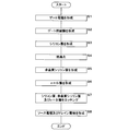
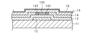
- FIG. 3 is a process diagram showing a manufacturing method of the TFT according to the first embodiment.
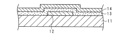
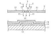
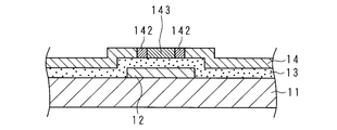
- 5, and 7 to 9 are schematic cross-sectional views showing a part of the manufacturing process of the TFT according to the first embodiment.
- the gate electrode 12 is formed on the substrate 11 (S1)
- the gate insulating film 13 is formed on the surface of the substrate 11 so as to cover the gate electrode 12 (S2)
- the surface of the gate insulating film 13 is formed.
- a silicon layer 14 made of amorphous silicon is formed (S3).
- FIG. 6 is a schematic plan view of the mask 2.
- the mask 2 has a flat plate shape, a shielding part 21 that shields the laser light 3, a first transmission part 22 that transmits the laser light 3, and a laser beam 3 that is transmitted at a lower transmittance than the first transmission part 22.
- the second transmission part 23 is included.
- the first transmission part 22 is made of a transparent material
- the second transmission part 23 is made of a single polarizing plate
- the shielding part 21 is made of two polarizing plates with the polarization directions orthogonal to each other.
- the shape of the first transmission part 22 is the same as that of the first polycrystalline part 142 shown in FIG. 2, and the shape of the second transmission part 23 is as shown in FIG.
- FIG. 8 shows a state in which the n + Si layer 16 is formed.
- the silicon layer 14 is covered with the amorphous silicon layer 15, and the n + Si layer 16 is covering the amorphous silicon layer 15.
- exposure processing and development processing are performed to form a required pattern with a photoresist on the n + Si layer 16, and the silicon layer 14, the amorphous silicon layer 15 and the n + Si layer 16 are etched (S7).
- FIG. 9 shows the state after etching.
- step S7 etching is performed so as to leave the amorphous silicon portion included in the silicon layer.
- the portion of amorphous silicon remaining in the silicon layer 14 becomes an amorphous portion 141.
- the source electrode 17 and the drain electrode 18 are formed on the n + Si layer 16 (S8), and the TFT is completed.
- the silicon layer 14 included in the channel layer of the TFT is more crystalline than the amorphous portion 141, the first polycrystalline portion 142, and the first polycrystalline portion 142. 2nd polycrystalline part 143 with low.
- the mobility is larger than that of the amorphous portion 141 and smaller than that of the first polycrystalline portion 142. Due to the presence of the second polycrystalline portion 143, the TFT characteristics such as mobility can be adjusted more appropriately than a TFT having a single crystallinity of the polycrystalline portion.
- the silicon layer 14 there are two first positions: a position including a part of the position where the source electrode 17 is projected and a position including a part of the position where the drain electrode 18 is projected.
- a polycrystalline portion 142 is formed.
- the second polycrystalline portion 143 connects the two first polycrystalline portions 142 in the silicon layer 14.
- the current flowing between the source electrode 17 and the drain electrode 18 flows through the first polycrystalline portion 142 and the second polycrystalline portion 143.
- a part of the position where the source electrode 17 and the drain electrode 18 are projected onto the silicon layer 14 is a part of the end of the silicon layer 14, and this part is an amorphous part 141.
- the current flowing between the source electrode 17 and the drain electrode 18 is affected by the amorphous portion 141, and the leakage current is reduced.
- the TFT according to this embodiment has lower mobility than the TFT in which the position where the source electrode 17 and the drain electrode 18 are projected onto the silicon layer 14 is connected by the first polycrystalline portion 142 as in the conventional TFT. Leakage current is reduced.
- the TFT according to the present embodiment is more leaky than the conventional TFT in which the amorphous portion 141 is formed between the two first polycrystalline portions 142 in the silicon layer 14. Although the current increases, the mobility increases. Therefore, in this embodiment mode, the mobility and leakage current in the TFT can be adjusted to moderate levels, and both the improvement in mobility and the reduction in leakage current can be achieved.
- the silicon layer 14 is irradiated with the laser beam 3 through the mask 2 including the shielding part 21, the first transmission part 22, and the second transmission part 23.
- a crystal part 142 and a second polycrystal part 143 are formed.
- the position, shape and size of the first transmission part 22 and the second transmission part 23 in the mask 2 the position and shape of the first polycrystalline part 142 and the second polycrystalline part 143 in the silicon layer 14. And the size can be adjusted.
- the crystallinity of the second polycrystalline portion 143 can be adjusted by adjusting the transmittance of the laser light 3 in the second transmitting portion 23.
- the mobility and leakage current in the TFT are determined according to the position, shape, and size of the first polycrystalline portion 142 and the second polycrystalline portion 143 and the crystallinity of the second polycrystalline portion 143. Therefore, it is possible to easily adjust the TFT characteristics by adjusting the configuration of the mask 2.
- the first polycrystalline portion 142 and the second polycrystalline portion 143 are formed in the silicon layer 14 using the mask 2, but the first polycrystalline portion 142 is formed by other methods. It is also possible to form the second polycrystalline portion 143. For example, by changing the output of the laser light according to the irradiation position on the silicon layer 14, the portion to be the second polycrystalline portion 143 is compared with the case where the portion to be the first polycrystalline portion 142 is irradiated. When irradiating, the intensity of the laser beam may be lowered. Further, for example, different lasers may be used depending on the irradiation position on the silicon layer 14.
- FIG. 10 is a schematic plan view of a main part of the TFT according to the second embodiment.
- the cross-sectional structure of the TFT is the same as that of the first embodiment.
- FIG. 10 shows the positional relationship of the silicon layer 14, the source electrode 17, and the drain electrode 18 in a plan view, and other structures of the TFT are omitted.
- First polycrystalline portions 142 are formed at two locations in the silicon layer 14, and the two first polycrystalline portions 142 are separated from each other in plan view.
- One first polycrystalline portion 142 includes a part of the position where the source electrode 17 is projected onto the silicon layer 14, and the other first polycrystalline portion 142 is a position where the drain electrode 18 is projected onto the silicon layer 14. Part of
Landscapes
- Thin Film Transistor (AREA)
- Recrystallisation Techniques (AREA)
Abstract
L'invention concerne un transistor à couches minces (TCM), dans lequel des caractéristiques sont ajustées d'une manière appropriée par ajustement de la cristallinité du silicium polycristallin, ainsi qu'un procédé de fabrication du transistor à couches minces. Une couche de silicium 14 incluse dans une couche de canal d'un TCM comprend une section amorphe 141, une première section polycristalline 142 et une seconde section polycristalline 143 ayant une plus faible cristallinité. La première section polycristalline 142 et la seconde section polycristalline 143 sont formées par exposition de la couche de silicium 14 à une lumière laser (faisceau d'énergie) à travers un masque 2 qui comprend une section de blocage 21 qui bloque la lumière laser, une première section de transmission qui transmet la lumière laser et une seconde section de blocage 22 ayant un plus faible facteur de transmission de la lumière laser. Par comparaison à des TCM dans lesquels la cristallinité d'une partie polycristalline est d'un seul type, des caractéristiques de TCM, telles que la mobilité, sont ajustées d'une manière plus appropriée par inclusion de la seconde section polycristalline 143. En outre, les caractéristiques du TCM peuvent être ajustées simplement par ajustement de la configuration du masque 2.
Priority Applications (4)
| Application Number | Priority Date | Filing Date | Title |
|---|---|---|---|
| CN201580083197.2A CN108028201B (zh) | 2015-09-17 | 2015-09-17 | 薄膜晶体管和薄膜晶体管的制造方法 |
| PCT/JP2015/076592 WO2017046932A1 (fr) | 2015-09-17 | 2015-09-17 | Transistor à couches minces et procédé de fabrication de transistor à couches minces |
| JP2017540427A JP6483271B2 (ja) | 2015-09-17 | 2015-09-17 | 薄膜トランジスタ及び薄膜トランジスタの製造方法 |
| US15/923,697 US10263121B2 (en) | 2015-09-17 | 2018-03-16 | Thin film transistor and method of manufacturing thin film transistor |
Applications Claiming Priority (1)
| Application Number | Priority Date | Filing Date | Title |
|---|---|---|---|
| PCT/JP2015/076592 WO2017046932A1 (fr) | 2015-09-17 | 2015-09-17 | Transistor à couches minces et procédé de fabrication de transistor à couches minces |
Related Child Applications (1)
| Application Number | Title | Priority Date | Filing Date |
|---|---|---|---|
| US15/923,697 Continuation-In-Part US10263121B2 (en) | 2015-09-17 | 2018-03-16 | Thin film transistor and method of manufacturing thin film transistor |
Publications (1)
| Publication Number | Publication Date |
|---|---|
| WO2017046932A1 true WO2017046932A1 (fr) | 2017-03-23 |
Family
ID=58288406
Family Applications (1)
| Application Number | Title | Priority Date | Filing Date |
|---|---|---|---|
| PCT/JP2015/076592 Ceased WO2017046932A1 (fr) | 2015-09-17 | 2015-09-17 | Transistor à couches minces et procédé de fabrication de transistor à couches minces |
Country Status (4)
| Country | Link |
|---|---|
| US (1) | US10263121B2 (fr) |
| JP (1) | JP6483271B2 (fr) |
| CN (1) | CN108028201B (fr) |
| WO (1) | WO2017046932A1 (fr) |
Cited By (1)
| Publication number | Priority date | Publication date | Assignee | Title |
|---|---|---|---|---|
| US20200006394A1 (en) * | 2018-06-28 | 2020-01-02 | Sakai Display Products Corporation | Thin film transistor, display device and method for producing thin film transistor |
Families Citing this family (3)
| Publication number | Priority date | Publication date | Assignee | Title |
|---|---|---|---|---|
| US20190140102A1 (en) * | 2016-04-25 | 2019-05-09 | Sakai Display Products Corporation | Thin film transistor, display device, and thin film transistor manufacturing method |
| CN110137261A (zh) * | 2018-10-29 | 2019-08-16 | 京东方科技集团股份有限公司 | 薄膜晶体管及其制备方法、阵列基板和显示装置 |
| CN113748521B (zh) * | 2020-03-27 | 2024-09-13 | 京东方科技集团股份有限公司 | 薄膜晶体管及其制备方法、阵列基板、显示装置 |
Citations (4)
| Publication number | Priority date | Publication date | Assignee | Title |
|---|---|---|---|---|
| JPH06342909A (ja) * | 1990-08-29 | 1994-12-13 | Internatl Business Mach Corp <Ibm> | 薄膜トランジスタ及びその製法 |
| JP2008140984A (ja) * | 2006-12-01 | 2008-06-19 | Sharp Corp | 半導体素子、半導体素子の製造方法、及び表示装置 |
| JP2011029411A (ja) * | 2009-07-24 | 2011-02-10 | V Technology Co Ltd | 薄膜トランジスタ、その製造方法及び液晶表示装置 |
| WO2011161910A1 (fr) * | 2010-06-22 | 2011-12-29 | パナソニック株式会社 | Dispositif d'affichage électroluminescent et son procédé de fabrication |
Family Cites Families (9)
| Publication number | Priority date | Publication date | Assignee | Title |
|---|---|---|---|---|
| JPH05226656A (ja) * | 1992-02-13 | 1993-09-03 | Hitachi Ltd | 薄膜半導体装置及びその製造方法 |
| JPH0775237B2 (ja) * | 1992-11-27 | 1995-08-09 | シャープ株式会社 | 電界効果トランジスタの製造方法 |
| EP0955674B1 (fr) * | 1998-04-28 | 2011-07-13 | Xerox Corporation | Fabrication de structures hybrides à silicium polycristallin et amorphe |
| JP2010177325A (ja) * | 2009-01-28 | 2010-08-12 | Seiko Epson Corp | 薄膜トランジスターの製造方法 |
| JP2012114131A (ja) | 2010-11-22 | 2012-06-14 | Panasonic Corp | 薄膜トランジスタ、その製造方法、および表示装置 |
| TWI570920B (zh) * | 2011-01-26 | 2017-02-11 | 半導體能源研究所股份有限公司 | 半導體裝置及其製造方法 |
| KR20130078666A (ko) * | 2011-12-30 | 2013-07-10 | 삼성디스플레이 주식회사 | 박막 트랜지스터 및 그 제조 방법 |
| CN104037127A (zh) * | 2014-06-11 | 2014-09-10 | 京东方科技集团股份有限公司 | 一种多晶硅层及显示基板的制备方法、显示基板 |
| CN104599959A (zh) * | 2014-12-24 | 2015-05-06 | 深圳市华星光电技术有限公司 | 低温多晶硅tft基板的制作方法及其结构 |
-
2015
- 2015-09-17 WO PCT/JP2015/076592 patent/WO2017046932A1/fr not_active Ceased
- 2015-09-17 CN CN201580083197.2A patent/CN108028201B/zh not_active Expired - Fee Related
- 2015-09-17 JP JP2017540427A patent/JP6483271B2/ja not_active Expired - Fee Related
-
2018
- 2018-03-16 US US15/923,697 patent/US10263121B2/en not_active Expired - Fee Related
Patent Citations (4)
| Publication number | Priority date | Publication date | Assignee | Title |
|---|---|---|---|---|
| JPH06342909A (ja) * | 1990-08-29 | 1994-12-13 | Internatl Business Mach Corp <Ibm> | 薄膜トランジスタ及びその製法 |
| JP2008140984A (ja) * | 2006-12-01 | 2008-06-19 | Sharp Corp | 半導体素子、半導体素子の製造方法、及び表示装置 |
| JP2011029411A (ja) * | 2009-07-24 | 2011-02-10 | V Technology Co Ltd | 薄膜トランジスタ、その製造方法及び液晶表示装置 |
| WO2011161910A1 (fr) * | 2010-06-22 | 2011-12-29 | パナソニック株式会社 | Dispositif d'affichage électroluminescent et son procédé de fabrication |
Cited By (2)
| Publication number | Priority date | Publication date | Assignee | Title |
|---|---|---|---|---|
| US20200006394A1 (en) * | 2018-06-28 | 2020-01-02 | Sakai Display Products Corporation | Thin film transistor, display device and method for producing thin film transistor |
| US11133333B2 (en) * | 2018-06-28 | 2021-09-28 | Sakai Display Products Corporation | Producing method for thin film transistor with different crystallinities |
Also Published As
| Publication number | Publication date |
|---|---|
| US10263121B2 (en) | 2019-04-16 |
| JPWO2017046932A1 (ja) | 2018-07-26 |
| CN108028201A (zh) | 2018-05-11 |
| CN108028201B (zh) | 2021-06-04 |
| JP6483271B2 (ja) | 2019-03-13 |
| US20180212065A1 (en) | 2018-07-26 |
Similar Documents
| Publication | Publication Date | Title |
|---|---|---|
| JP6503458B2 (ja) | 薄膜トランジスタの製造方法及び表示パネル | |
| CN107408578B (zh) | 薄膜晶体管以及显示面板 | |
| KR101193585B1 (ko) | 열처리에 의해 얼라인먼트 마크를 형성한 반도체박막을가지는 반도체장치, 반도체박막의 결정화방법, 및반도체박막의 결정화장치 | |
| US9640569B2 (en) | Doping method for array substrate and manufacturing equipment of the same | |
| US10038098B2 (en) | Method for manufacturing thin film transistor, thin film transistor and display panel | |
| JP5593182B2 (ja) | 逐次的横方向結晶化方法 | |
| JP6483271B2 (ja) | 薄膜トランジスタ及び薄膜トランジスタの製造方法 | |
| WO2017042941A1 (fr) | Dispositif d'affichage et procédé de fabrication de dispositif d'affichage | |
| KR20080078290A (ko) | 폴리 실리콘 결정화용 마스크 및 이를 이용한 폴리 실리콘기판 제조 방법 | |
| JP2006222423A (ja) | レーザー装置及びこれを利用した薄膜トランジスタの製造方法 | |
| WO2010131502A1 (fr) | Transistor à film mince et son procédé de fabrication | |
| US20070006796A1 (en) | Crystallization apparatus and crystallization method | |
| JP4763983B2 (ja) | 光変調素子、結晶化装置、結晶化方法、薄膜半導体基板の製造装置、薄膜半導体基板の製造方法、薄膜半導体装置、薄膜半導体装置の製造方法、表示装置及び位相シフタ | |
| US20200020530A1 (en) | Laser irradiation device, method of manufacturing thin film transistor, program, and projection mask | |
| JP2011139082A (ja) | 光変調素子、結晶化装置、結晶化方法、薄膜半導体基板の製造装置、薄膜半導体基板の製造方法、薄膜半導体装置、薄膜半導体装置の製造方法および表示装置 | |
| KR20090073479A (ko) | 액정표시장치용 어레이 기판 및 그의 제조방법 | |
| CN108630711A (zh) | Tft阵列基板的制作方法及tft阵列基板 | |
| JP2009099797A (ja) | 半導体薄膜の結晶化方法、薄膜半導体装置の製造方法及び液晶表示装置の製造方法 | |
| WO2019107108A1 (fr) | Dispositif d'irradiation laser, procédé d'irradiation laser et masque de projection | |
| JP2005116558A (ja) | 半導体薄膜の結晶化方法並びに結晶化装置、及び、半導体装置並びに製造方法、及び表示装置 | |
| CN111033693A (zh) | 激光照射装置、薄膜晶体管的制造方法、程序及投影掩模 | |
| JP2009060128A (ja) | 位相シフトマスク | |
| KR20110070599A (ko) | 박막트랜지스터 및 평판형 표시장치 제조방법 |
Legal Events
| Date | Code | Title | Description |
|---|---|---|---|
| 121 | Ep: the epo has been informed by wipo that ep was designated in this application |
Ref document number: 15904119 Country of ref document: EP Kind code of ref document: A1 |
|
| ENP | Entry into the national phase |
Ref document number: 2017540427 Country of ref document: JP Kind code of ref document: A |
|
| NENP | Non-entry into the national phase |
Ref country code: DE |
|
| 122 | Ep: pct application non-entry in european phase |
Ref document number: 15904119 Country of ref document: EP Kind code of ref document: A1 |