WO2017104055A1 - Unité de capture d'images, endoscope et procédé de fabrication pour unité de capture d'image - Google Patents
Unité de capture d'images, endoscope et procédé de fabrication pour unité de capture d'image Download PDFInfo
- Publication number
- WO2017104055A1 WO2017104055A1 PCT/JP2015/085415 JP2015085415W WO2017104055A1 WO 2017104055 A1 WO2017104055 A1 WO 2017104055A1 JP 2015085415 W JP2015085415 W JP 2015085415W WO 2017104055 A1 WO2017104055 A1 WO 2017104055A1
- Authority
- WO
- WIPO (PCT)
- Prior art keywords
- solid
- inner lead
- fold
- imaging unit
- valley
- Prior art date
- Legal status (The legal status is an assumption and is not a legal conclusion. Google has not performed a legal analysis and makes no representation as to the accuracy of the status listed.)
- Ceased
Links
Images




Classifications
-
- A—HUMAN NECESSITIES
- A61—MEDICAL OR VETERINARY SCIENCE; HYGIENE
- A61B—DIAGNOSIS; SURGERY; IDENTIFICATION
- A61B1/00—Instruments for performing medical examinations of the interior of cavities or tubes of the body by visual or photographical inspection, e.g. endoscopes; Illuminating arrangements therefor
- A61B1/04—Instruments for performing medical examinations of the interior of cavities or tubes of the body by visual or photographical inspection, e.g. endoscopes; Illuminating arrangements therefor combined with photographic or television appliances
-
- H—ELECTRICITY
- H04—ELECTRIC COMMUNICATION TECHNIQUE
- H04N—PICTORIAL COMMUNICATION, e.g. TELEVISION
- H04N25/00—Circuitry of solid-state image sensors [SSIS]; Control thereof
- H04N25/70—SSIS architectures; Circuits associated therewith
-
- H—ELECTRICITY
- H10—SEMICONDUCTOR DEVICES; ELECTRIC SOLID-STATE DEVICES NOT OTHERWISE PROVIDED FOR
- H10F—INORGANIC SEMICONDUCTOR DEVICES SENSITIVE TO INFRARED RADIATION, LIGHT, ELECTROMAGNETIC RADIATION OF SHORTER WAVELENGTH OR CORPUSCULAR RADIATION
- H10F99/00—Subject matter not provided for in other groups of this subclass
Definitions
- the present invention relates to an imaging unit that is provided at the distal end of an insertion portion of an endoscope that is inserted into a subject and images the inside of the subject, an endoscope, and a method for manufacturing the imaging unit.
- endoscopes have been widely used for various examinations in the medical field and the industrial field.
- medical endoscopes incise a subject by inserting an elongated flexible insertion portion having an imaging element at the tip into the body cavity of the subject such as a patient. Since an in-vivo image in a body cavity can be acquired at least and a treatment tool can be projected from the distal end of the insertion portion as necessary, it is widely used.
- a flexible print such as a TAB (Tape Automated Bonding) on which a solid-state image sensor and electronic components such as a capacitor and an IC chip constituting a drive circuit of the solid-state image sensor are mounted at the distal end of the insertion portion of the endoscope.
- An imaging unit including a board hereinafter referred to as an FPC board
- a signal cable is soldered to the FPC board of the imaging unit.
- Inner leads exposed from the end face of the FPC board are connected to electrode pads formed on the solid-state imaging device. At the time of this connection, the inner lead is bent from the side surface of the solid-state imaging device along the light receiving surface side and connected to the electrode pad (for example, see Patent Document 1).
- Patent Document 1 in order to avoid a short circuit due to contact between the wiring layer and the solid-state imaging device, the exposed inner lead portion is shortened, and the electrical insulating layer covering the wiring layer is brought into contact with the side surface of the solid-state imaging device. Yes.
- an imaging unit in which the exposed portion of the inner lead is lengthened to shorten the aperture around the solid-state imaging device, and an imaging unit using an FPC board that does not have an electrical insulating layer are available. It is being considered.
- the inner lead and the solid-state imaging device are sealed with a sealing resin for insulation.
- the present invention has been made in view of the above, and includes an imaging unit, an endoscope, and an imaging unit that can reduce the diameter of the imaging unit and ensure insulation between the inner lead and the solid-state imaging device.
- An object is to provide a manufacturing method.
- an imaging unit includes a solid-state imaging device that generates an electrical signal by receiving light and performing photoelectric conversion, an insulating base material, A wiring layer formed on the substrate, and a surface facing the light receiving surface of the solid-state image sensor along the optical axis direction of the solid-state image sensor when the light incident direction is the front.
- a flexible printed circuit board extending rearward from a back surface, and a laminated board connected to the wiring layer side of the flexible printed circuit board and mounted with a plurality of electronic components, wherein the wiring layer is exposed from the base material.
- the inner lead connected to the electrode pad of the solid-state imaging device has a first mountain-shaped fold that protrudes toward the laminated substrate, and the position of the first mountain-shaped fold is the position of the solid-state imaging device. Be behind the back And features.
- the electrode pad is formed in a region other than a region where the light receiving unit is formed on the front surface of the solid-state imaging device, and the inner lead is the first lead. It has the 1st trough-shaped crease which becomes a concave in the said laminated substrate side in the front side from this mountain-shaped crease.
- the imaging unit according to the present invention is characterized in that, in the above invention, the inner lead has a second valley-shaped fold that is recessed toward the laminated substrate side behind the first mountain-shaped fold. To do.
- the imaging unit according to the present invention is characterized in that, in the above invention, the first mountain-shaped fold is in contact with the laminated substrate.
- the imaging unit according to the present invention is the imaging device according to the above invention, wherein the inner lead has a second mountain-shaped fold that protrudes toward the solid-state imaging device side in the vicinity of the end connected to the electrode pad of the solid-state imaging device. It is characterized by having.
- the inner lead is a third recess that is recessed toward the solid-state imaging device between the second mountain-shaped fold and the first valley-shaped fold. It has a valley-like fold.
- the inner leads are arranged in order from the end side, the second mountain-shaped fold, the third valley-shaped fold, the first valley-shaped fold, the first The first valley fold and the second valley fold; the distance between the second valley fold and the laminated substrate; the first valley fold and the third valley fold; The distance between the inner lead and the solid-state image sensor is substantially the same.
- the imaging unit according to the present invention includes a glass lid that covers the light receiving surface of the solid-state imaging device, and the third valley-shaped fold is located behind the surface side of the glass lid.
- the imaging unit according to the present invention is characterized in that, in the above invention, the fold of the inner lead is perpendicular to the longitudinal direction of the inner lead.
- an endoscope according to the present invention is characterized in that the imaging unit according to any one of the above is provided with an insertion portion provided at a distal end.
- the manufacturing method of the imaging unit according to the present invention is the manufacturing method of the imaging unit according to any one of the above, wherein an insulating base material, a wiring layer formed on the base material, A fold forming step of forming a crease with a mold on an inner lead exposed from the base material of the flexible printed circuit board, and a flying lead exposed from the base material of the flexible printed circuit board via an electrode of the laminated substrate A first connection step for connecting to the electrode, and an end of the inner lead connected to the electrode pad of the solid-state imaging device that receives the light and performs photoelectric conversion to generate an electric signal through the bump. And a third connecting step of connecting a side surface of the multilayer substrate and a back surface that is a surface facing the light receiving surface of the solid-state imaging device.
- the imaging unit and the endoscope can be reduced in diameter while preventing a short circuit.
- FIG. 1 is a diagram schematically showing an overall configuration of an endoscope system according to an embodiment of the present invention.
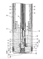
- FIG. 2 is a partial cross-sectional view of the distal end of the endoscope shown in FIG.
- FIG. 3 is a side view of the imaging unit shown in FIG.
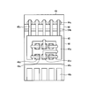
- FIG. 4 is a bottom view of the imaging unit of FIG.
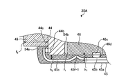
- FIG. 5 is a partially enlarged view of the imaging unit of FIG.
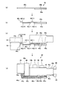
- FIG. 6 is a diagram illustrating a manufacturing process of the imaging unit shown in FIG.
- FIG. 7 is a partially enlarged view of an imaging unit according to Modification 1 of the embodiment of the present invention.
- FIG. 8 is a partially enlarged view of an imaging unit according to the second modification of the embodiment of the present invention.
- FIG. 9 is a partially enlarged view of an imaging unit according to Modification 3 of the embodiment of the present invention.
- FIG. 10 is a partially enlarged view of an imaging unit according to Modification 4 of the embodiment of the present invention.
- an endoscope provided with an imaging unit will be described as a mode for carrying out the present invention (hereinafter referred to as “embodiment”). Moreover, this invention is not limited by this embodiment. Furthermore, the same code
- FIG. 1 is a diagram schematically showing an overall configuration of an endoscope system according to an embodiment of the present invention.
- the endoscope system 1 includes an endoscope 2, a universal cord 6, a connector 7, a light source device 9, a processor (control device) 10, and a display device 13.
- the endoscope 2 captures an in-vivo image of the subject and outputs an imaging signal by inserting the insertion portion 4 into the body cavity of the subject.
- the electric cable bundle inside the universal cord 6 extends to the distal end of the insertion portion 4 of the endoscope 2 and is connected to an imaging device provided at the distal end portion 31 of the insertion portion 4.
- the connector 7 is provided at the base end of the universal cord 6, is connected to the light source device 9 and the processor 10, and performs predetermined signal processing on the imaging signal output from the imaging device of the distal end portion 31 connected to the universal cord 6.
- the image pickup signal is converted from analog to digital (A / D conversion) and output as an image signal.
- the light source device 9 is configured using, for example, a white LED.
- the pulsed white light that is turned on by the light source device 9 becomes illumination light that is irradiated toward the subject from the distal end of the insertion portion 4 of the endoscope 2 via the connector 7 and the universal cord 6.
- the processor 10 performs predetermined image processing on the image signal output from the connector 7 and controls the entire endoscope system 1.
- the display device 13 displays the image signal processed by the processor 10.
- the operation part 5 provided with various buttons and knobs for operating the endoscope function is connected to the proximal end side of the insertion part 4 of the endoscope 2.
- the operation unit 5 is provided with a treatment instrument insertion port 17 for inserting treatment instruments such as a biological forceps, an electric knife and an inspection probe into the body cavity of the subject.
- the insertion section 4 is connected to the distal end portion 31 where the imaging device is provided, the bending portion 32 that is connected to the proximal end side of the distal end portion 31 and bendable in a plurality of directions, and the proximal end side of the bending portion 32. And the flexible tube portion 33.
- the bending portion 32 is bent by the operation of a bending operation knob provided in the operation portion 5, and can be bent in, for example, four directions, up, down, left and right, as the bending wire inserted into the insertion portion 4 is pulled and loosened. Yes.
- the endoscope 2 is provided with a light guide bundle (not shown) that transmits illumination light from the light source device 9, and an illumination lens (not shown) is arranged at the exit end of the illumination light from the light guide bundle.
- This illumination lens is provided at the distal end portion 31 of the insertion portion 4, and the illumination light is irradiated toward the subject.
- FIG. 2 is a partial cross-sectional view of the distal end of the endoscope 2.
- 2 is a cross-sectional view taken along a plane that is orthogonal to the substrate surface of the imaging unit provided at the distal end portion 31 of the endoscope 2 and is parallel to the optical axis direction of the imaging unit. is there.
- a distal end portion 31 of the insertion portion 4 of the endoscope 2 and a part of the bending portion 32 are illustrated.
- the bending portion 32 can be bent in four directions, up, down, left, and right, as the bending wire 82 inserted inside the bending tube 81 disposed inside the cladding tube 42 described later is pulled and loosened.
- An imaging device 40 is provided inside the distal end portion 31 extended to the distal end side of the curved portion 32.
- the imaging device 40 includes a lens unit 43 and an imaging unit 35 disposed on the proximal end side of the lens unit 43, and is adhered to the inside of the distal end body 41 with an adhesive 41a.
- the tip end body 41 is formed of a hard member for forming an internal space for accommodating the imaging device 40.
- the proximal end outer peripheral portion of the distal end portion main body 41 is covered with a flexible cladding tube 42.
- the member on the base end side with respect to the distal end portion main body 41 is formed of a flexible member so that the bending portion 32 can be bent.
- the distal end portion 31 where the distal end portion main body 41 is disposed is a hard portion of the insertion portion 4.
- the lens unit 43 includes a plurality of objective lenses 43a-1 to 43a-4 and a lens holder 43b that holds the objective lenses 43a-1 to 43a-4.
- the tip of the lens holder 43b is the tip portion main body 41. It is fixed to the tip end body 41 by being inserted and fixed inside.
- the imaging unit 35 receives light from a CCD or CMOS, etc., and performs photoelectric conversion to generate an electrical signal, and the back side facing the light receiving surface on which the light receiving portion 44a of the solid state imaging device 44 is formed.
- a flexible printed circuit board 45 (hereinafter referred to as “FPC board 45”) extending to the surface, a laminated board 46 having a plurality of conductor layers formed on the surface of the FPC board 45, and a solid-state image sensor 44 covering the light receiving surface of the solid-state image sensor 44
- a glass lid 49 that adheres to the image sensor 44 is provided.
- an electronic component 55 which is an active component constituting a driving circuit of the solid-state imaging device 44, and an electronic component 56 such as a passive component are mounted. Vias for electrical conduction are formed. Further, the laminated substrate 46 has a stepped portion 46a on the proximal end side where an external electrode 46b that connects the distal ends of the signal cables 48 of the electric cable bundle 47 is formed (see FIGS. 3 and 4).
- each signal cable 48 extends in the base end direction of the insertion portion 4.
- the electric cable bundle 47 is inserted into the insertion portion 4 and extends to the connector 7 via the operation portion 5 and the universal cord 6 shown in FIG.
- the subject images formed by the objective lenses 43a-1 to 43a-4 of the lens unit 43 are detected by the solid-state imaging device 44 provided at the imaging positions of the objective lenses 43a-1 to 43a-4, and imaged. Converted to a signal.
- the imaging signal is output to the processor 10 via the signal cable 48 and the connector 7 connected to the FPC board 45 and the laminated board 46.
- the solid-state imaging device 44 is bonded to the side surface of the multilayer substrate 46 on the back side facing the light receiving surface on which the light receiving portion 44a is formed.
- the outer periphery of the side surface of the solid-state imaging device 44 is covered with a metal reinforcing member 52.
- the reinforcing member 52 is installed separately from the solid-state imaging device 44, the FPC substrate 45 and the multilayer substrate 46.
- the outer periphery of the image pickup unit 35 and the tip of the electric cable bundle 47 is covered with a heat shrinkable tube 50 in order to improve resistance. Inside the heat shrinkable tube 50, a gap between components is filled with an adhesive resin 51.
- the solid-state image sensor holder 53 holds the solid-state image sensor 44 that adheres to the glass lid 49 by fitting the outer peripheral surface of the glass lid 49 to the inner peripheral surface of the base end side of the solid-state image sensor holder 53.
- the proximal end side outer peripheral surface of the solid-state image sensor holder 53 is fitted to the distal end side inner peripheral surface of the reinforcing member 52.
- the base end side outer peripheral surface of the lens holder 43 b is fitted to the front end side inner peripheral surface of the solid-state image sensor holder 53.
- the outer peripheral surface of the lens holder 43b, the outer peripheral surface of the solid-state imaging device holder 53, and the outer peripheral surface of the distal end side of the heat shrinkable tube 50 are bonded to the distal end portion main body 41 by the adhesive 41a. It is fixed to the inner peripheral surface of the tip.
- FIG. 3 is a side view of the imaging unit 35 shown in FIG.
- FIG. 4 is a bottom view of the imaging unit 35 of FIG.
- FIG. 5 is a partially enlarged view of the imaging unit of FIG.
- the FPC board 45 includes an insulating base material 45a and a wiring layer 45b formed on the base material 45a, on the back side facing the light receiving surface on which the light receiving portion 44a of the solid-state imaging device 44 is formed. Extend.
- the FPC board 45 has an inner lead 45c and a flying lead 45d in which the wiring layer 45b is exposed from the base material 45a, and the inner lead 45c exposed from the tip is provided on the electrode pad 44b of the solid-state imaging device 44 via the bump 44c. Connected electrically and mechanically.
- the flying lead 45d exposed inside the FPC board 45 is electrically and mechanically connected to the electrode pad 46c of the multilayer board 46 via the bump 46d.
- connection portion between the inner lead 45c and the electrode pad 44b, between the inner lead 45c and the side surface of the solid-state imaging device 44, and between the FPC board 45 and the multilayer substrate 46 including the connection portion between the flying lead 45d and the electrode pad 46c. Is covered with an insulating sealing resin 54a.
- the back surface side of the solid-state image sensor 44 and the side surface of the multilayer substrate 46 on the solid-state image sensor side are bonded by an adhesive 54b.
- the inner lead 45c is formed with a first chevron fold 45f-1 and a second chevron fold 45f-2 that protrude toward the laminated substrate 46 or the solid-state imaging device 44 side.
- a first valley-like fold 45e-1, a second valley-like fold 45e-2, and a third valley-like fold 45e-3 that are concave are formed on the laminated substrate 46 or the solid-state imaging device 44 side.
- a second mountain-shaped fold 45f-2, a third valley-shaped fold 45e-3, a first valley-shaped fold 45e-1, a first mountain-shaped fold 45f-1, A second valley fold 45e-2 is formed. Note that these folds are folds in a direction perpendicular to the longitudinal direction of the inner lead 45c (the optical axis direction of the imaging unit 35).
- the first mountain-shaped fold 45f-1 and the first valley-shaped fold 45e-1 are formed so as to be located behind the back surface f1 of the light receiving surface of the solid-state imaging device 44 when the light incident direction is the front. By doing so, it is possible to prevent occurrence of a short circuit due to contact between the inner lead 45c and the side surface of the solid-state imaging device 44.
- the first mountain fold 45f-1 is preferably in contact with the bottom surface of the multilayer substrate 46.
- stress is applied to the inner lead 45c. Even when the shape of the inner lead 45c is deformed due to the contact, it is possible to prevent the solid-state imaging element 44 from contacting the side surface.
- the distance h2 between the inner lead 45c between the first valley-like fold 45e-1 and the third valley-like fold 45e-3 and the side surface of the solid-state imaging device 44 is equal to the second valley-like fold 45e.
- the position of each fold is preferably adjusted so as to be substantially the same as the distance h1 between -2 and the laminated substrate 46, that is, the distance between the wiring layer 45b and the laminated substrate 46.
- the third valley-like fold 45e-3 is located behind the surface f2 side of the glass lid 49, preferably behind the half of the thickness t1 of the glass lid 49 in the optical axis direction from the surface f2 side of the glass lid 49. It is preferable to form as follows. By adjusting the position of the third valley fold 45e-3 as described above, the image pickup unit 35 can be easily held in the solid-state image sensor holder 53.
- FIG. 6 is a diagram for explaining a manufacturing process of the imaging unit 35.
- a crease is formed on the inner lead 45c exposed from the FPC board 45 by a mold or the like (see FIGS. 6A and 6B).
- the FPC board 45 is connected to the laminated board 46 and the solid-state imaging device 44 (see FIG. 6C).
- the FPC board 45 is connected to the multilayer substrate 46 and the solid-state imaging device 44 by connecting the flying lead 45d to the electrode pad 46b of the multilayer substrate 46 and then connecting the end of the inner lead 45c to the electrode pad 44b of the solid-state imaging device 44.
- the flying lead 45d may be connected to the electrode pad 46c of the multilayer substrate 46.
- the FPC board 45 is connected to the multilayer substrate 46 and the solid-state imaging device 44, the inner leads 45c are bent, and the back side of the solid-state imaging device 44 and the side surface of the multilayer substrate 46 are bonded with an adhesive 54b (FIG. 6D). reference). Further, the FPC board 45 and the laminated board 46 including the periphery of the connection portion between the inner lead 45c and the electrode pad 44b, the connection between the inner lead 45c and the side surface of the solid-state imaging device 44, and the connection portion between the flying lead 45d and the electrode pad 46c.
- the imaging unit 35 is manufactured by filling and sealing the sealing resin 54a.
- the imaging unit 35 can prevent a short circuit because the inner lead 45c does not contact the side surface of the solid-state imaging device 44 by forming a plurality of folds in the inner lead 45c. Further, since only the inner lead 45c and the sealing resin 54a are present on the outer periphery of the side surface of the solid-state imaging device 44, the imaging unit 35 can be reduced in diameter. Further, by forming a crease around the connecting portion between the inner lead 45c and the electrode pad 44b, the crease absorbs the stress even when stress is applied to the inner lead 45c. Therefore, the inner lead 45c and the electrode pad 44b The stress applied to the connecting portion can be reduced, and peeling of the inner lead 45c can be prevented.
- the second mountain fold 45f-2, the third valley fold 45e-3, the first valley fold 45e-1, and the first valley fold 45f-2 are formed from the end of the inner lead 45c.
- the positional deviation can be adjusted by each crease even when there is a positional deviation of the connecting portion.
- the FPC board 45 includes only the insulating base material 45a and the wiring layer 45b has been described.
- the image pickup unit Shortening can be prevented while reducing the diameter.
- a similar crease is provided in the inner lead 45c exposed from one of the wiring layers, and the first mountain-shaped fold 45f-1 is formed.
- FIG. 7 is a partially enlarged view of an imaging unit according to Modification 1 of the embodiment of the present invention.
- the first mountain-shaped fold 45f-1 that protrudes toward the laminated substrate 46 is formed behind the back side of the solid-state imaging device 44 of the inner lead 45c.
- the imaging unit 35A can be reduced in diameter.
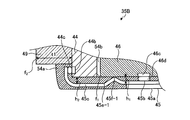
- FIG. 8 is a partially enlarged view of an imaging unit according to the second modification of the embodiment of the present invention.
- the first mountain-shaped fold 45f-1 that protrudes toward the laminated substrate 46 is formed behind the solid-state imaging element 44 of the inner lead 45c, and the laminated substrate A first valley-like fold 45e-1 that is concave on the 46 side is formed on the end side from the first mountain-like fold 45f-1.
- the first mountain-shaped fold 45f-1 and the first valley-shaped fold 45e-1 it is possible to prevent a short circuit due to contact of the inner lead 45c with the side surface of the solid-state imaging device 44.
- the first valley-like fold 45e-1 the distance h2 between the inner lead 45c and the side surface of the solid-state imaging element 44 can be easily controlled, and the imaging unit 35B can be easily reduced in diameter.
- FIG. 9 is a partially enlarged view of an imaging unit according to Modification 3 of the embodiment of the present invention.
- the first mountain-shaped fold 45f-1 that protrudes toward the laminated substrate 46 is formed behind the back surface f1 side of the solid-state imaging device 44 of the inner lead 45c.
- a third valley fold 45e-3 that is concave on the side of 44 is formed in the vicinity of the connecting portion between the inner lead 45c and the electrode pad 44b, and a first valley fold 45e-1 that is concave on the side of the laminated substrate 46 is formed. Is formed between the first mountain-shaped fold 45f-1 and the third valley-shaped fold 45e-3.
- the first mountain-shaped fold 45f-1 and the first valley-shaped fold 45e-1 By providing the first mountain-shaped fold 45f-1 and the first valley-shaped fold 45e-1, it is possible to prevent a short circuit due to contact of the inner lead 45c with the side surface of the solid-state imaging device 44.
- the distance h2 between the inner lead 45c and the side surface of the solid-state imaging device 44 can be easily controlled, and the imaging unit 35C can be easily reduced in diameter.
- the third valley-like fold 45e-3 the stress applied to the connecting portion between the inner lead 45c and the electrode pad 44b can be reduced, and the inner lead 45c can be prevented from being peeled off.
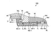
- FIG. 10 is a partially enlarged view of an imaging unit according to Modification 4 of the embodiment of the present invention.
- the first mountain fold 45f-1 that protrudes toward the laminated substrate 46 is formed behind the back side of the solid-state imaging device 44 of the inner lead 45c.
- a third valley fold 45e-3 that is concave toward the solid-state image sensor 44 and a second mountain fold that is convex toward the solid-state image sensor 44 are provided in the vicinity of the connection portion between the inner lead 45c and the electrode pad 44b.
- 45f-2 is formed in the vicinity of the connection portion between the inner lead 45c and the electrode pad 44b.
- a first valley fold 45e-1 that is concave on the side of the laminated substrate 46 is formed between the first mountain fold 45f-1 and the third valley fold 45e-3.
- the first mountain-shaped fold 45f-1 and the first valley-shaped fold 45e-1 it is possible to prevent a short circuit due to contact of the inner lead 45c with the side surface of the solid-state imaging device 44.
- the first valley-like fold 45e-1 the distance h2 between the inner lead 45c and the side surface of the solid-state imaging element 44 can be easily controlled, and the imaging unit 35D can be easily reduced in diameter.
- the third valley-shaped fold 45e-3 and the second mountain-shaped fold 45f-2 the stress applied to the connecting portion between the inner lead 45c and the electrode pad 44b can be reduced, and the inner lead 45c is peeled off.
- the distance h2 between the inner lead 45c and the side surface of the solid-state imaging device 44 can be easily controlled even when the connecting portion is misaligned.
Landscapes
- Health & Medical Sciences (AREA)
- Life Sciences & Earth Sciences (AREA)
- Surgery (AREA)
- Engineering & Computer Science (AREA)
- Radiology & Medical Imaging (AREA)
- Heart & Thoracic Surgery (AREA)
- Biophysics (AREA)
- Nuclear Medicine, Radiotherapy & Molecular Imaging (AREA)
- Optics & Photonics (AREA)
- Pathology (AREA)
- Signal Processing (AREA)
- Multimedia (AREA)
- Biomedical Technology (AREA)
- Physics & Mathematics (AREA)
- Medical Informatics (AREA)
- Molecular Biology (AREA)
- Animal Behavior & Ethology (AREA)
- General Health & Medical Sciences (AREA)
- Public Health (AREA)
- Veterinary Medicine (AREA)
- Endoscopes (AREA)
- Transforming Light Signals Into Electric Signals (AREA)
- Studio Devices (AREA)
Abstract
La présente invention a pour objet de réaliser une unité de capture d'images, un endoscope, et un procédé de fabrication d'une unité de capture d'images, par lequel le diamètre de l'unité de capture d'images peut être réduit et l'isolation entre un conducteur interne et un élément de capture d'images à semiconducteur peut être obtenue. L'élément de capture d'images (35) selon l'invention est pourvu des éléments suivants : un élément de capture d'images à semiconducteur (44) ; un substrat d'impression flexible (45) qui comprend un matériau de base isolant (45a) et une couche de câblage (45b) formée sur le matériau de base (45a), et qui s'étend jusqu'à un côté de surface arrière qui est une surface opposée à une surface de réception de lumière de l'élément de capture d'images à semiconducteur (44) ; et un substrat stratifié (46) qui est relié au côté de la couche de câblage (45b) du substrat d'impression flexible (45) et sur lequel sont montés des composants électroniques (55, 56). L'élément de capture d'image est caractérisé en ce que : la couche de câblage (45b) est exposée depuis le matériau de base (45a) ; un fil intérieur (45c) est relié à une pastille d'électrode (44b) de l'élément de capture d'images à semiconducteur (44) et comprend un premier coude en forme de crête (45f-1) qui fait saillie vers le côté du substrat stratifié (46) ; et la position du premier coude en forme de crête (45f-1) est plus éloignée en arrière qu'une surface arrière (f1) de la surface réceptrice de lumière de l'élément de capture d'images à semiconducteur (44).
Priority Applications (2)
| Application Number | Priority Date | Filing Date | Title |
|---|---|---|---|
| JP2017556282A JPWO2017104055A1 (ja) | 2015-12-17 | 2015-12-17 | 撮像ユニット、内視鏡および撮像ユニットの製造方法 |
| PCT/JP2015/085415 WO2017104055A1 (fr) | 2015-12-17 | 2015-12-17 | Unité de capture d'images, endoscope et procédé de fabrication pour unité de capture d'image |
Applications Claiming Priority (1)
| Application Number | Priority Date | Filing Date | Title |
|---|---|---|---|
| PCT/JP2015/085415 WO2017104055A1 (fr) | 2015-12-17 | 2015-12-17 | Unité de capture d'images, endoscope et procédé de fabrication pour unité de capture d'image |
Publications (1)
| Publication Number | Publication Date |
|---|---|
| WO2017104055A1 true WO2017104055A1 (fr) | 2017-06-22 |
Family
ID=59056242
Family Applications (1)
| Application Number | Title | Priority Date | Filing Date |
|---|---|---|---|
| PCT/JP2015/085415 Ceased WO2017104055A1 (fr) | 2015-12-17 | 2015-12-17 | Unité de capture d'images, endoscope et procédé de fabrication pour unité de capture d'image |
Country Status (2)
| Country | Link |
|---|---|
| JP (1) | JPWO2017104055A1 (fr) |
| WO (1) | WO2017104055A1 (fr) |
Citations (4)
| Publication number | Priority date | Publication date | Assignee | Title |
|---|---|---|---|---|
| JP2000083896A (ja) * | 1998-09-11 | 2000-03-28 | Olympus Optical Co Ltd | 内視鏡用撮像装置 |
| JP2005329093A (ja) * | 2004-05-21 | 2005-12-02 | Pentax Corp | 電子内視鏡の固体撮像装置 |
| JP2015066300A (ja) * | 2013-09-30 | 2015-04-13 | オリンパス株式会社 | 撮像ユニットおよび内視鏡装置 |
| WO2015125776A1 (fr) * | 2014-02-24 | 2015-08-27 | オリンパス株式会社 | Dispositif d'imagerie, et procédé de fabrication d'un dispositif d'imagerie |
-
2015
- 2015-12-17 JP JP2017556282A patent/JPWO2017104055A1/ja not_active Ceased
- 2015-12-17 WO PCT/JP2015/085415 patent/WO2017104055A1/fr not_active Ceased
Patent Citations (4)
| Publication number | Priority date | Publication date | Assignee | Title |
|---|---|---|---|---|
| JP2000083896A (ja) * | 1998-09-11 | 2000-03-28 | Olympus Optical Co Ltd | 内視鏡用撮像装置 |
| JP2005329093A (ja) * | 2004-05-21 | 2005-12-02 | Pentax Corp | 電子内視鏡の固体撮像装置 |
| JP2015066300A (ja) * | 2013-09-30 | 2015-04-13 | オリンパス株式会社 | 撮像ユニットおよび内視鏡装置 |
| WO2015125776A1 (fr) * | 2014-02-24 | 2015-08-27 | オリンパス株式会社 | Dispositif d'imagerie, et procédé de fabrication d'un dispositif d'imagerie |
Also Published As
| Publication number | Publication date |
|---|---|
| JPWO2017104055A1 (ja) | 2018-11-01 |
Similar Documents
| Publication | Publication Date | Title |
|---|---|---|
| JP6396650B2 (ja) | 撮像ユニットおよび内視鏡装置 | |
| JP6351228B2 (ja) | 撮像モジュールおよび内視鏡装置 | |
| US9345395B2 (en) | Imaging module and endoscope device | |
| US20180070803A1 (en) | Imaging device and endoscope system | |
| JP5973761B2 (ja) | ケーブル接続構造 | |
| CN106999023B (zh) | 摄像单元、内窥镜以及摄像单元的制造方法 | |
| JP6570657B2 (ja) | 撮像装置、内視鏡および撮像装置の製造方法 | |
| JP6205228B2 (ja) | 撮像モジュールおよび内視鏡装置 | |
| JP4578913B2 (ja) | 撮像装置 | |
| WO2018155066A1 (fr) | Endoscope | |
| US10517465B2 (en) | Cable connection structure and endoscope apparatus | |
| US10191270B2 (en) | Imaging unit and endoscope apparatus | |
| JP6099541B2 (ja) | 内視鏡及び内視鏡の製造方法 | |
| WO2017115441A1 (fr) | Structure de montage, dispositif de prise de vue et endoscope | |
| JP6503205B2 (ja) | 撮像装置 | |
| JPWO2017104055A1 (ja) | 撮像ユニット、内視鏡および撮像ユニットの製造方法 |
Legal Events
| Date | Code | Title | Description |
|---|---|---|---|
| 121 | Ep: the epo has been informed by wipo that ep was designated in this application |
Ref document number: 15910745 Country of ref document: EP Kind code of ref document: A1 |
|
| ENP | Entry into the national phase |
Ref document number: 2017556282 Country of ref document: JP Kind code of ref document: A |
|
| NENP | Non-entry into the national phase |
Ref country code: DE |
|
| 122 | Ep: pct application non-entry in european phase |
Ref document number: 15910745 Country of ref document: EP Kind code of ref document: A1 |