WO2017104513A1 - Procédé de fabrication de substrat de support en verre - Google Patents
Procédé de fabrication de substrat de support en verre Download PDFInfo
- Publication number
- WO2017104513A1 WO2017104513A1 PCT/JP2016/086427 JP2016086427W WO2017104513A1 WO 2017104513 A1 WO2017104513 A1 WO 2017104513A1 JP 2016086427 W JP2016086427 W JP 2016086427W WO 2017104513 A1 WO2017104513 A1 WO 2017104513A1
- Authority
- WO
- WIPO (PCT)
- Prior art keywords
- glass substrate
- supporting glass
- supporting
- heat treatment
- substrate
- Prior art date
- Legal status (The legal status is an assumption and is not a legal conclusion. Google has not performed a legal analysis and makes no representation as to the accuracy of the status listed.)
- Ceased
Links
Images

Classifications
-
- C—CHEMISTRY; METALLURGY
- C03—GLASS; MINERAL OR SLAG WOOL
- C03B—MANUFACTURE, SHAPING, OR SUPPLEMENTARY PROCESSES
- C03B32/00—Thermal after-treatment of glass products not provided for in groups C03B19/00, C03B25/00 - C03B31/00 or C03B37/00, e.g. crystallisation, eliminating gas inclusions or other impurities; Hot-pressing vitrified, non-porous, shaped glass products
-
- B—PERFORMING OPERATIONS; TRANSPORTING
- B24—GRINDING; POLISHING
- B24B—MACHINES, DEVICES, OR PROCESSES FOR GRINDING OR POLISHING; DRESSING OR CONDITIONING OF ABRADING SURFACES; FEEDING OF GRINDING, POLISHING, OR LAPPING AGENTS
- B24B7/00—Machines or devices designed for grinding plane surfaces on work, including polishing plane glass surfaces; Accessories therefor
- B24B7/20—Machines or devices designed for grinding plane surfaces on work, including polishing plane glass surfaces; Accessories therefor characterised by a special design with respect to properties of the material of non-metallic articles to be ground
- B24B7/22—Machines or devices designed for grinding plane surfaces on work, including polishing plane glass surfaces; Accessories therefor characterised by a special design with respect to properties of the material of non-metallic articles to be ground for grinding inorganic material, e.g. stone, ceramics, porcelain
- B24B7/24—Machines or devices designed for grinding plane surfaces on work, including polishing plane glass surfaces; Accessories therefor characterised by a special design with respect to properties of the material of non-metallic articles to be ground for grinding inorganic material, e.g. stone, ceramics, porcelain for grinding or polishing glass
- B24B7/242—Machines or devices designed for grinding plane surfaces on work, including polishing plane glass surfaces; Accessories therefor characterised by a special design with respect to properties of the material of non-metallic articles to be ground for grinding inorganic material, e.g. stone, ceramics, porcelain for grinding or polishing glass for plate glass
-
- B—PERFORMING OPERATIONS; TRANSPORTING
- B32—LAYERED PRODUCTS
- B32B—LAYERED PRODUCTS, i.e. PRODUCTS BUILT-UP OF STRATA OF FLAT OR NON-FLAT, e.g. CELLULAR OR HONEYCOMB, FORM
- B32B17/00—Layered products essentially comprising sheet glass, or glass, slag, or like fibres
-
- C—CHEMISTRY; METALLURGY
- C03—GLASS; MINERAL OR SLAG WOOL
- C03B—MANUFACTURE, SHAPING, OR SUPPLEMENTARY PROCESSES
- C03B17/00—Forming molten glass by flowing-out, pushing-out, extruding or drawing downwardly or laterally from forming slits or by overflowing over lips
- C03B17/06—Forming glass sheets
- C03B17/064—Forming glass sheets by the overflow downdraw fusion process; Isopipes therefor
-
- C—CHEMISTRY; METALLURGY
- C03—GLASS; MINERAL OR SLAG WOOL
- C03B—MANUFACTURE, SHAPING, OR SUPPLEMENTARY PROCESSES
- C03B33/00—Severing cooled glass
- C03B33/02—Cutting or splitting sheet glass or ribbons; Apparatus or machines therefor
-
- H—ELECTRICITY
- H10—SEMICONDUCTOR DEVICES; ELECTRIC SOLID-STATE DEVICES NOT OTHERWISE PROVIDED FOR
- H10P—GENERIC PROCESSES OR APPARATUS FOR THE MANUFACTURE OR TREATMENT OF DEVICES COVERED BY CLASS H10
- H10P72/00—Handling or holding of wafers, substrates or devices during manufacture or treatment thereof
- H10P72/70—Handling or holding of wafers, substrates or devices during manufacture or treatment thereof for supporting or gripping
-
- H—ELECTRICITY
- H10—SEMICONDUCTOR DEVICES; ELECTRIC SOLID-STATE DEVICES NOT OTHERWISE PROVIDED FOR
- H10W—GENERIC PACKAGES, INTERCONNECTIONS, CONNECTORS OR OTHER CONSTRUCTIONAL DETAILS OF DEVICES COVERED BY CLASS H10
- H10W70/00—Package substrates; Interposers; Redistribution layers [RDL]
- H10W70/60—Insulating or insulated package substrates; Interposers; Redistribution layers
-
- H—ELECTRICITY
- H10—SEMICONDUCTOR DEVICES; ELECTRIC SOLID-STATE DEVICES NOT OTHERWISE PROVIDED FOR
- H10W—GENERIC PACKAGES, INTERCONNECTIONS, CONNECTORS OR OTHER CONSTRUCTIONAL DETAILS OF DEVICES COVERED BY CLASS H10
- H10W70/00—Package substrates; Interposers; Redistribution layers [RDL]
- H10W70/60—Insulating or insulated package substrates; Interposers; Redistribution layers
- H10W70/67—Insulating or insulated package substrates; Interposers; Redistribution layers characterised by their insulating layers or insulating parts
- H10W70/68—Shapes or dispositions thereof
-
- H—ELECTRICITY
- H10—SEMICONDUCTOR DEVICES; ELECTRIC SOLID-STATE DEVICES NOT OTHERWISE PROVIDED FOR
- H10W—GENERIC PACKAGES, INTERCONNECTIONS, CONNECTORS OR OTHER CONSTRUCTIONAL DETAILS OF DEVICES COVERED BY CLASS H10
- H10W70/00—Package substrates; Interposers; Redistribution layers [RDL]
- H10W70/60—Insulating or insulated package substrates; Interposers; Redistribution layers
- H10W70/67—Insulating or insulated package substrates; Interposers; Redistribution layers characterised by their insulating layers or insulating parts
- H10W70/69—Insulating materials thereof
- H10W70/692—Ceramics or glasses
-
- H—ELECTRICITY
- H10—SEMICONDUCTOR DEVICES; ELECTRIC SOLID-STATE DEVICES NOT OTHERWISE PROVIDED FOR
- H10W—GENERIC PACKAGES, INTERCONNECTIONS, CONNECTORS OR OTHER CONSTRUCTIONAL DETAILS OF DEVICES COVERED BY CLASS H10
- H10W72/00—Interconnections or connectors in packages
- H10W72/20—Bump connectors, e.g. solder bumps or copper pillars; Dummy bumps; Thermal bumps
-
- H—ELECTRICITY
- H10—SEMICONDUCTOR DEVICES; ELECTRIC SOLID-STATE DEVICES NOT OTHERWISE PROVIDED FOR
- H10W—GENERIC PACKAGES, INTERCONNECTIONS, CONNECTORS OR OTHER CONSTRUCTIONAL DETAILS OF DEVICES COVERED BY CLASS H10
- H10W76/00—Containers; Fillings or auxiliary members therefor; Seals
- H10W76/10—Containers or parts thereof
-
- H—ELECTRICITY
- H10—SEMICONDUCTOR DEVICES; ELECTRIC SOLID-STATE DEVICES NOT OTHERWISE PROVIDED FOR
- H10W—GENERIC PACKAGES, INTERCONNECTIONS, CONNECTORS OR OTHER CONSTRUCTIONAL DETAILS OF DEVICES COVERED BY CLASS H10
- H10W72/00—Interconnections or connectors in packages
- H10W72/01—Manufacture or treatment
- H10W72/0198—Manufacture or treatment batch processes
-
- H—ELECTRICITY
- H10—SEMICONDUCTOR DEVICES; ELECTRIC SOLID-STATE DEVICES NOT OTHERWISE PROVIDED FOR
- H10W—GENERIC PACKAGES, INTERCONNECTIONS, CONNECTORS OR OTHER CONSTRUCTIONAL DETAILS OF DEVICES COVERED BY CLASS H10
- H10W72/00—Interconnections or connectors in packages
- H10W72/20—Bump connectors, e.g. solder bumps or copper pillars; Dummy bumps; Thermal bumps
- H10W72/241—Dispositions, e.g. layouts
-
- Y—GENERAL TAGGING OF NEW TECHNOLOGICAL DEVELOPMENTS; GENERAL TAGGING OF CROSS-SECTIONAL TECHNOLOGIES SPANNING OVER SEVERAL SECTIONS OF THE IPC; TECHNICAL SUBJECTS COVERED BY FORMER USPC CROSS-REFERENCE ART COLLECTIONS [XRACs] AND DIGESTS
- Y02—TECHNOLOGIES OR APPLICATIONS FOR MITIGATION OR ADAPTATION AGAINST CLIMATE CHANGE
- Y02P—CLIMATE CHANGE MITIGATION TECHNOLOGIES IN THE PRODUCTION OR PROCESSING OF GOODS
- Y02P40/00—Technologies relating to the processing of minerals
- Y02P40/50—Glass production, e.g. reusing waste heat during processing or shaping
- Y02P40/57—Improving the yield, e-g- reduction of reject rates
Definitions
- the present invention relates to a method for manufacturing a supporting glass substrate, and specifically to a method for manufacturing a supporting glass substrate for supporting a processed substrate in a manufacturing process of a semiconductor package.
- Portable electronic devices such as mobile phones, notebook personal computers, and PDAs (Personal Data Assistance) are required to be smaller and lighter.
- the mounting space of semiconductor chips used in these electronic devices is also strictly limited, and high-density mounting of semiconductor chips has become a problem. Therefore, in recent years, high-density mounting of semiconductor packages has been achieved by three-dimensional mounting technology, that is, by stacking semiconductor chips and interconnecting the semiconductor chips.
- a conventional wafer level package is manufactured by forming bumps in a wafer state and then separating them by dicing.
- the semiconductor chip is likely to be chipped.
- the fan-out type WLP can increase the number of pins, and can prevent chipping of the semiconductor chip by protecting the end portion of the semiconductor chip.
- the fan-out type WLP includes a step of forming a processed substrate by molding a plurality of semiconductor chips with a resin sealing material and then wiring to one surface of the processed substrate, a step of forming a solder bump, and the like.
- the sealing material may be deformed and the processed substrate may change in dimensions.
- the dimension of the processed substrate changes, it becomes difficult to perform wiring with high density on one surface of the processed substrate, and it becomes difficult to accurately form solder bumps.
- the glass substrate is easy to smooth the surface and has rigidity. Therefore, when a glass substrate is used as the support substrate, the processed substrate can be supported firmly and accurately. In addition, the glass substrate easily transmits light such as ultraviolet light and infrared light. Therefore, when a glass substrate is used as the support substrate, the processed substrate and the glass substrate can be easily fixed by providing an adhesive layer or the like with an ultraviolet curable adhesive or the like. Furthermore, if a release layer or the like that absorbs infrared rays is provided, the processed substrate and the glass substrate can be easily separated. As another method, when an adhesive layer or the like is provided by an ultraviolet curable tape or the like, the processed substrate and the glass substrate can be easily fixed and separated.
- the thermal expansion coefficient of the glass substrate was matched with the thermal expansion coefficient of the processed substrate.
- the thermal expansion coefficient of the glass substrate may deviate from the target value due to fluctuations in the melting conditions and molding conditions of the glass substrate. In this case, the glass substrate is discarded or the glass substrate is re-melted to change the thermal expansion coefficient of the glass substrate, resulting in an increase in the manufacturing cost of the glass substrate.
- This invention is made
- the technical subject is to devise the method which can readjust the thermal expansion coefficient of the support glass substrate after shaping
- the present inventor has found that the above technical problem can be solved by performing heat treatment on the glass substrate after forming, and proposes as the present invention. That is, the method for producing a supporting glass substrate of the present invention is a method for producing a supporting glass substrate for supporting a processed substrate. The forming step of forming the supporting glass substrate and the supporting glass substrate after forming are heat-treated and supported. And a heat treatment step for varying the thermal expansion coefficient of the glass substrate.
- the thermal expansion coefficient of the supporting glass substrate can be changed to the target value by heat treatment. This eliminates the need for disposal and remelting of the supporting glass substrate, and can reduce the manufacturing cost of the supporting glass substrate.
- the method for producing a supporting glass substrate of the present invention it is preferable to heat-treat the supporting glass substrate after the forming step to reduce the thermal expansion coefficient of the supporting glass substrate.
- the maximum temperature of the heat treatment is higher than (strain point of supporting glass substrate ⁇ 100) ° C.
- the heat treatment temperature it is preferable to lower the heat treatment temperature at a rate of 5 ° C./min or less after reaching the maximum temperature of the heat treatment.
- the amount of warpage of the supporting glass substrate is the sum of the absolute value of the maximum distance between the highest point and the least square focal plane in the entire supporting crystallized glass substrate and the absolute value of the lowest point and the least square focal plane.
- the "warp amount” can be measured by SBW-331ML / d manufactured by Kobelco Kaken.
- the method for producing a supporting glass substrate of the present invention is to prepare a heat treatment setter larger than the size of the supporting glass substrate, and after placing the formed supporting glass substrate on the heat treatment setter, heat treatment is performed. It is preferable to use for a process.
- the method for producing a supporting glass substrate of the present invention it is preferable to mold the supporting glass substrate so that the plate thickness is 400 ⁇ m or more and less than 2 mm.
- the method for producing a supporting glass substrate of the present invention preferably forms the supporting glass substrate by an overflow down draw method.
- the method for manufacturing a supporting glass substrate of the present invention includes a polishing step of polishing the surface of the supporting glass substrate after the heat treatment step to reduce the overall thickness deviation to less than 2.0 ⁇ m.
- the “total plate thickness deviation” is a difference between the maximum plate thickness and the minimum plate thickness of the entire support glass substrate, and can be measured by, for example, SBW-331ML / d manufactured by Kobelco Kaken.
- the method for manufacturing a supporting glass substrate of the present invention includes a cutting and removing step of cutting and removing the peripheral portion of the supporting glass substrate after the heat treatment step.
- the method for manufacturing a semiconductor package of the present invention includes a stacking step of manufacturing a laminate including at least a processing substrate and a supporting glass substrate for supporting the processing substrate, and a processing substrate of the stack, It is preferable that the supporting glass substrate is produced by the manufacturing method of the supporting glass substrate.
- the processed substrate includes a semiconductor chip molded with at least a sealing material.
- the processing includes a process of wiring on one surface of the processed substrate.
- the processing process includes a process of forming a solder bump on one surface of the processed substrate.
- glass raw materials are first prepared and mixed to prepare a glass batch. After the glass batch is put into a glass melting furnace, the obtained molten glass is clarified and stirred. Thus, it is preferable to supply a forming apparatus and form a plate to obtain a supporting glass substrate.
- the glass batch is preferably prepared so as to have a desired thermal expansion coefficient. Specifically, when the ratio of semiconductor chips in the processed substrate is small and the ratio of the sealing material is large, a glass batch is prepared so as to have a high expansion glass composition, and conversely, the semiconductor chips are processed in the processed substrate. When the ratio is large and the ratio of the sealing material is small, it is preferable to prepare a glass batch so as to obtain a low expansion glass composition.
- the supporting glass substrate has a glass composition in mass%, SiO 2 55-75%, Al 2 O 3 15-30%, Li 2 O 0.1-6%, Na 2 O + K 2 O (total amount of Na 2 O and K 2 O) 0-8%, MgO + CaO + SrO + BaO ( The total amount of MgO, CaO, SrO and BaO) It is preferable to prepare a glass batch so as to contain 0-10%, SiO 2 55-75%, Al 2 O 3 10-30%, Li 2 O + Na 2 O + K 2 O (Li 2 O, the total content of Na 2 O and K 2 O) 0 ⁇ 0.3% , it is also preferred to prepare the glass batch to contain MgO + CaO + SrO + BaO 5 ⁇ 20%, Si 2 55 ⁇ 6
- the supporting glass substrate has a glass composition in mass%, SiO 2 55 to 75%, Al 2 O 3 3 to 15%, B 2 O 3 5 to 20%, MgO 0 to 5%, CaO 0 to 10%, SrO 0 to 5%, BaO 0 to 5%, ZnO It is preferred to prepare the glass batch to contain 0-5%, Na 2 O 5-15%, K 2 O 0-10%, SiO 2 64-71%, Al 2 O 3 5-10%, B 2 O 3 8-15%, MgO 0-5%, CaO 0-6%, SrO 0-3%, BaO 0-3%, ZnO 0-3%, Na 2 O 5-15%, K 2 O More preferably, the glass batch is prepared to contain 0-5%.
- the supporting glass substrate has a glass composition in mass%, SiO 2 60-75%, Al 2 O 3 5-15%, B 2 O 3 5-20%, MgO 0-5%, CaO 0-10%, SrO 0-5%, BaO 0-5%, ZnO It is preferred to prepare the glass batch to contain 0-5%, Na 2 O 7-16%, K 2 O 0-8%, SiO 2 60-68%, Al 2 O 3 5-15%, B 2 O 3 5-20%, MgO 0-5%, CaO 0-10%, SrO 0-3%, BaO 0-3%, ZnO 0-3%, Na 2 O 8-16%, K 2 O More preferably, the glass batch is prepared to contain 0-3%.
- the supporting glass substrate has a glass composition in mass%, SiO 2 45-70% (55-70%), Al 2 O 3 3-25% (preferably 3-13%), B 2 O 3 0-8% (preferably 2-8%), P 2 O 5 0 ⁇ 20%, MgO 0 ⁇ 5%, CaO 0 ⁇ 10%, SrO 0 ⁇ 5%, BaO 0 ⁇ 5%, ZnO 0 ⁇ 5%, Na 2 O 10 ⁇ 21%, K 2 O 0 ⁇ 5 It is preferred to prepare the glass batch to contain%.
- the supporting glass substrate has a glass composition in mass%, SiO 2 53-65%, Al 2 O 3 3-13%, B 2 O 3 0-5%, MgO 0.1-6%, CaO 0-10%, SrO 0-5%, BaO 0-5% , ZnO 0 ⁇ 5%, Na 2 O + K 2 O 20 ⁇ 40%, Na 2 O 12 ⁇ 21%, it is preferable to prepare the glass batch to contain K 2 O 7 ⁇ 21%.
- Average linear thermal expansion coefficient in the temperature range of 30 to 380 ° C.” refers to a value measured with a dilatometer.
- One kind selected from the group of As 2 O 3 , Sb 2 O 3 , CeO 2 , SnO 2 , F, Cl, SO 3 (preferably a group of SnO 2 , Cl, SO 3 ) as a fining agent in the glass batch
- two or more kinds may be added in an amount of 0.05 to 2% by mass.
- the total amount of SnO 2 , SO 3 and Cl is preferably 0 to 1% by mass, 100 to 3000 ppm (0.01 to 0.3% by mass), 300 to 2500 ppm, particularly 500 to 2500 ppm.
- the total amount of SnO 2 , SO 3 and Cl is less than 100 ppm, it becomes difficult to enjoy the clarification effect.
- substantially does not contain specifically means that the content of the explicit component is less than 500 ppm (mass). From an environmental point of view, it is also preferable that the glass composition does not substantially contain PbO or Bi 2 O 3 .
- the Young's modulus of the supporting glass substrate is 60 GPa or more (desirably 65 GPa or more, 70 GPa or more, particularly 75 to 130 GPa).
- the ratio of the semiconductor chip is small and the ratio of the sealing material is large in the processed substrate, the rigidity of the entire laminated body is lowered, and the processed substrate is easily warped in the processing step. Therefore, when the Young's modulus of the supporting glass substrate is increased, it becomes easy to suppress warping deformation of the processed substrate, and the processed substrate can be supported firmly and accurately.
- Young's modulus refers to a value measured by a bending resonance method.
- the liquidus temperature of the supporting glass substrate is less than 1150 ° C (desirably 1120 ° C or lower, 1100 ° C or lower, 1080 ° C or lower, 1050 ° C or lower, 1010 ° C or lower, 980 ° C or lower, 960 ° C or lower, 950 ° C or lower, especially 940 ° C or lower.
- the liquid phase viscosity of the supporting glass substrate is 10 4.8 dPa ⁇ s or more (desirably 10 5.0 dPa ⁇ s or more, 10 5.2 dPa ⁇ s or more, 10 5.4 dPa ⁇ s or more, particularly 10 5 It is preferable to prepare a glass batch so that it may become 6 dPa * s or more. In this way, the support glass substrate can be easily formed by the downdraw method, particularly the overflow downdraw method, so that it is easy to produce a support glass substrate having a small thickness, and the entire plate can be obtained without polishing the surface. Thickness deviation can be reduced.
- the overall plate thickness deviation can be reduced to less than 2.0 ⁇ m, particularly less than 1.0 ⁇ m, by a small amount of polishing.
- the “liquid phase temperature” is obtained by passing the standard sieve 30 mesh (500 ⁇ m) and putting the glass powder remaining on the 50 mesh (300 ⁇ m) into a platinum boat, and holding it in a temperature gradient furnace for 24 hours. It can be calculated by measuring the temperature of precipitation.
- the “liquid phase viscosity” can be measured by a platinum ball pulling method.
- the plate thickness is 400 ⁇ m or more and less than 2 mm.
- the thickness of the supporting glass substrate is preferably 400 ⁇ m or more, 500 ⁇ m or more, 600 ⁇ m or more, 700 ⁇ m or more, 800 ⁇ m or more, 900 ⁇ m or more, particularly 1000 ⁇ m or more. If the thickness of the supporting glass substrate is too small, the mechanical strength is lowered, and the supporting glass substrate is easily damaged in the manufacturing process of the semiconductor package. On the other hand, since the mass of a laminated body will become large when the plate
- the thickness of the supporting glass substrate is preferably less than 2.0 mm, 1.5 mm or less, 1.2 mm or less, and particularly 1.1 mm or less.
- the molten glass overflows from both sides of the heat-resistant bowl-shaped structure, and the overflowing molten glass is merged at the lower top end of the bowl-shaped structure to form a molding joining surface inside the glass.
- This is a method of extending and forming downward.
- the surface to be the glass surface is not in contact with the bowl-like refractory, and is formed in a free surface state. For this reason, it becomes easy to produce a supporting glass substrate having a small plate thickness, and the overall plate thickness deviation can be reduced without polishing the surface.
- the overall plate thickness deviation can be reduced to less than 2.0 ⁇ m, particularly less than 1.0 ⁇ m, by a small amount of polishing. As a result, the manufacturing cost of the supporting glass substrate can be reduced.
- a method for forming the supporting glass substrate in addition to the overflow downdraw method, for example, a slot down method, a redraw method, a float method, or the like can be adopted.
- the method for producing a support glass substrate of the present invention preferably includes a step of measuring the thermal expansion coefficient of the support glass substrate after molding before the heat treatment step.
- the thermal expansion coefficient of the support glass substrate is controlled by controlling the heat treatment conditions (the maximum temperature of the heat treatment, the cooling rate of the heat treatment, etc.) in consideration of the measured value of the thermal expansion coefficient of the support glass substrate. It becomes easy to adjust to the target value.
- the supporting glass substrate manufacturing method of the present invention may include a supporting glass substrate cleaning step before the heat treatment step. Thereby, even if a foreign material adheres to the supporting glass substrate, the adhered foreign material can be prevented from being burned onto the surface of the supporting glass substrate by heat treatment.
- the method for producing a support glass substrate according to the present invention includes a heat treatment step of changing the thermal expansion coefficient of the support glass substrate by heat-treating the support glass substrate after forming, in which case the support glass substrate after the forming step is heat-treated. And it is preferable to reduce the thermal expansion coefficient of a support glass substrate. If it does in this way, it will become easy to control the thermal expansion coefficient of a support glass substrate to a target value. It is possible to increase the thermal expansion coefficient of the supporting glass substrate by heat treatment. In this case, the supporting glass substrate must be subjected to a heat treatment step after sufficiently cooling the supporting glass substrate at the time of molding. The production efficiency is likely to decrease.
- the average linear thermal expansion coefficient of the supporting glass substrate in the temperature range of 30 to 380 ° C. is preferably decreased by 0.05 ⁇ 10 ⁇ 7 to 3 ⁇ 10 ⁇ 7 / ° C., and 0.1 ⁇ 10 ⁇ 7 to More preferably, the temperature is lowered by 3 ⁇ 10 ⁇ 7 / ° C., more preferably by 0.2 ⁇ 10 ⁇ 7 to 1 ⁇ 10 ⁇ 7 / ° C., and 0.3 ⁇ 10 ⁇ 7 to 0.8 ⁇ 10 ⁇ It is particularly preferable to decrease the temperature by 7 / ° C.
- the coefficient of thermal expansion of the support glass substrate varies due to variations in melting conditions, molding conditions, and the like.
- the fluctuation range is not so large, these slight fluctuations become a problem in the use of the supporting glass substrate in which the thermal expansion coefficient needs to be adjusted strictly. It is difficult to control the thermal expansion coefficient to the target value by managing the melting conditions, the molding conditions, and the like. Therefore, by adjusting the heat treatment conditions (the maximum temperature of heat treatment, the temperature drop rate of heat treatment, etc.) in the heat treatment process, the thermal expansion coefficient of the supporting glass substrate can be controlled to the target value without strictly managing the melting conditions, molding conditions, etc. It becomes easy to do.
- the heat treatment conditions the maximum temperature of heat treatment, the temperature drop rate of heat treatment, etc.
- the method for producing a support glass substrate according to the present invention preferably includes a heat treatment step of changing the density of the support glass substrate by heat-treating the support glass substrate after forming, and in that case, heat-treating the support glass substrate after the forming step. Then, it is preferable to increase the density of the supporting glass substrate. This makes it easy to control the density of the supporting glass substrate to the target value when it is necessary to strictly adjust the density of the supporting glass substrate.
- the supporting glass substrate must be subjected to a heat treatment step after sufficiently cooling the supporting glass substrate at the time of molding. Efficiency tends to decrease.
- the degree of increase in the density of the supporting glass substrate correlates with the degree of decrease in the thermal expansion coefficient of the supporting glass substrate. Therefore, if the increase value of the density of the support glass substrate is measured, the decrease value of the thermal expansion coefficient of the support glass substrate can be easily estimated.
- the density of the supporting glass substrate 0.001 ⁇ 0.05g / cm 3 is raised, more preferably be 0.004 ⁇ 0.03g / cm 3 is raised, 0.007 ⁇ 0.015 g It is particularly preferable to increase / cm 3 . If the increase value of the density is out of the above range, it is difficult to estimate the decrease value of the thermal expansion coefficient of the support glass substrate.
- the maximum temperature of the heat treatment is preferably (strain point of supporting glass substrate ⁇ 100) ° C., (strain point of supporting glass substrate ⁇ 50) ° C. or more, (strain point of supporting glass substrate ⁇ 30) ° C. or more, supporting glass substrate (Strain point of supporting glass substrate + 10) ° C. or more, (strain point of supporting glass substrate + 20) ° C. or more, (strain point of supporting glass substrate + 30) ° C. or more, particularly (strain point of supporting glass substrate + 50 ) C or higher. If the maximum temperature of the heat treatment is too low, the heat treatment time for changing the thermal expansion coefficient of the support glass substrate becomes unreasonably long, and the heat treatment efficiency tends to decrease.
- the maximum temperature of the heat treatment is preferably (the strain point of the supporting glass substrate + 150) ° C. or less, and (the strain point of the supporting glass substrate + 120) ° C. or less.
- the cooling rate is preferably 5 ° C./min or less, 4 ° C./min or less, 3 ° C./min or less, 2 ° C./min or less, 1 ° C./min or less, particularly 0.8 ° C./min or less. If the temperature lowering rate is too fast, thermal strain tends to remain on the support glass substrate after the heat treatment step, and the support glass substrate may be damaged when the support glass substrate is taken out from the heat treatment furnace.
- the temperature decreasing rate is preferably 0.01 ° C./min or more, 0.05 ° C./min or more, 0.1 ° C./min or more, 0.2 ° C./min or more, particularly 0.5 ° C./min or more. .
- a heat-treating setter larger than the size of the supporting glass substrate, place the molded supporting glass substrate on the heat-treating setter, and then subject it to a heat treatment step. If it does in this way, the temperature nonuniformity of a support glass substrate can be reduced in the case of heat processing.
- the dimension of the setter for heat treatment is equal to or smaller than the dimension of the support glass substrate, a part of the support glass substrate is likely to protrude from the setter for heat treatment, and thermal deformation is likely to occur in the protruding portion.
- the method for producing a supporting glass substrate of the present invention it is preferable to reduce the amount of warpage of the supporting glass substrate to 40 ⁇ m or less by heat treatment. And in order to reduce the curvature amount of a support glass substrate, it is preferable to arrange
- the heat resistant substrate a mullite substrate, an alumina substrate, or the like can be used.
- the method for producing a supporting glass substrate of the present invention preferably includes a polishing step of polishing the surface of the supporting glass substrate after the heat treatment step to reduce the overall thickness deviation to less than 2.0 ⁇ m.
- a polishing treatment method Various methods can be adopted as the polishing treatment method.
- the supporting glass substrate is polished while the supporting glass substrate and the pair of polishing pads are rotated together by sandwiching both surfaces of the supporting glass substrate with the pair of polishing pads.
- the method of processing is preferred.
- the pair of polishing pads preferably have different outer diameters, and it is preferable to perform a polishing process so that a part of the supporting glass substrate protrudes from the polishing pad intermittently during polishing. This makes it easy to reduce the overall plate thickness deviation and to reduce the amount of warpage.
- the polishing depth is not particularly limited, but the polishing depth is preferably 50 ⁇ m or less, 30 ⁇ m or less, 20 ⁇ m or less, particularly 10 ⁇ m or less. As the polishing depth is smaller, the productivity of the supporting glass substrate is improved.
- the surface of the supporting glass substrate is preferably polished so that the thickness Ra is 5 nm or less, 2 nm or less, 1.5 nm or less, 1 nm or less, 0.8 nm or less, particularly 0.5 nm or less.
- the smaller the overall plate thickness deviation or the higher the surface accuracy the easier it is to improve the processing accuracy. In particular, since the wiring accuracy can be increased, high-density wiring is possible. Further, the strength of the supporting glass substrate is improved, and the supporting glass substrate and the laminate are hardly damaged.
- the “arithmetic average roughness Ra” can be measured by an atomic force microscope (AFM).
- the method for producing a supporting glass substrate of the present invention preferably includes a cutting and removing step of cutting and removing the peripheral portion of the supporting glass substrate after the heat treatment step, and cutting and removing the cutting and removing of the peripheral portion of the supporting glass substrate after the polishing step. More preferably, the method includes a step. In the heat treatment step, the amount of warpage tends to be larger in the peripheral portion than in the central portion of the supporting glass substrate. Therefore, if the peripheral portion of the supporting glass substrate is cut and removed after the heat treatment step, the amount of warpage of the supporting glass substrate can be reduced.
- the roundness (excluding the notch portion) of the cut support glass substrate is preferably 1 mm or less, 0.1 mm or less, 0.05 mm or less, and particularly preferably 0.03 mm or less. The smaller the roundness, the easier it is to apply to the semiconductor package manufacturing process.
- the definition of the roundness is a value obtained by subtracting the minimum value from the maximum value of the outer shape of the wafer.
- the method for producing a support glass substrate of the present invention preferably includes a notch processing step of forming a notch portion (alignment portion) on a part of the outer periphery of the support glass substrate after the cutting and removing step.
- a positioning member such as a positioning pin into contact with the notch portion of the support glass substrate.
- the processing substrate and the supporting glass substrate can be easily aligned.
- a notch part is formed also in a process board
- the method for producing a supporting glass substrate of the present invention preferably includes a chamfering step of chamfering the end surface (including the end surface of the notch portion) of the supporting glass substrate after the cutting and removing step. Thereby, it can prevent that glass powder etc. generate
- a chamfering process using a grindstone with a groove, a chamfering process using acid etching such as hydrofluoric acid, or the like can be adopted.
- the method for producing a supporting glass substrate of the present invention it is preferable not to perform ion exchange treatment on the supporting glass substrate.
- the ion exchange treatment is performed, the manufacturing cost of the supporting glass substrate increases, and it becomes difficult to reduce the overall thickness deviation of the supporting glass substrate.
- the manufacturing method of a semiconductor package of the present invention includes a stacking process for manufacturing a laminate including at least a processing substrate and a supporting glass substrate for supporting the processing substrate, and processing for performing processing on the processing substrate of the stack.
- a supporting glass substrate is produced by the above-described method for producing a supporting glass substrate.
- the adhesive layer is preferably a resin, for example, a thermosetting resin, a photocurable resin (particularly an ultraviolet curable resin), or the like.
- a resin for example, a thermosetting resin, a photocurable resin (particularly an ultraviolet curable resin), or the like.
- an ultraviolet curable tape can also be used as an adhesive layer.
- peeling of the processed substrate is preferably performed with irradiation light such as laser light from the viewpoint of productivity.
- irradiation light such as laser light from the viewpoint of productivity.
- the laser light source an infrared laser light source such as a YAG laser (wavelength 1064 nm) or a semiconductor laser (wavelength 780 to 1300 nm) can be used.
- a resin that decomposes when irradiated with an infrared laser can be used for the release layer.
- a substance that efficiently absorbs infrared rays and converts it into heat can also be added to the resin. For example, carbon black, graphite powder, fine metal powder, dye, pigment or the like can be added to the resin.
- the peeling layer is made of a material that causes “in-layer peeling” or “interfacial peeling” by irradiation light such as laser light. That is, when light of a certain intensity is irradiated, the bonding force between atoms or molecules in an atom or molecule disappears or decreases, and ablation or the like is caused to cause peeling.
- the component contained in the release layer is released as a gas due to irradiation of irradiation light, the separation layer is released, and when the release layer absorbs light and becomes a gas, and its vapor is released, resulting in separation There is.
- the dimension of the processed substrate is larger than the dimension of the supporting glass substrate.
- the method for manufacturing a semiconductor package of the present invention further includes a transporting process for transporting the stacked body.
- a transporting process for transporting the stacked body thereby, the processing efficiency of a processing process can be improved.
- the “conveying step” and the “processing step” are not necessarily performed separately, and may be performed simultaneously.
- the processing is preferably performed by wiring on one surface of the processed substrate or forming solder bumps on one surface of the processed substrate.
- the processing since the processed substrate is difficult to change in dimensions during these processes, these steps can be appropriately performed.
- one surface of a processed substrate (usually the surface opposite to the supporting glass substrate) is mechanically polished, and one surface of the processed substrate (usually a supporting glass substrate) Either a process of dry-etching the surface on the opposite side or a process of wet-etching one surface of the processed substrate (usually the surface opposite to the supporting glass substrate) may be used.
- the processed substrate is unlikely to warp and the rigidity of the stacked body can be maintained. As a result, the above processing can be performed appropriately.
- FIG. 1 is a conceptual perspective view showing an example of a laminate 1 according to the present invention.
- the laminate 1 includes a supporting glass substrate 10 and a processed substrate 11.
- the supporting glass substrate 10 is attached to the processed substrate 11 in order to prevent a dimensional change of the processed substrate 11.
- a release layer 12 and an adhesive layer 13 are disposed between the support glass substrate 10 and the processed substrate 11.
- the peeling layer 12 is in contact with the supporting glass substrate 10, and the adhesive layer 13 is in contact with the processed substrate 11.
- the laminate 1 is laminated in the order of the supporting glass substrate 10, the release layer 12, the adhesive layer 13, and the processed substrate 11.
- the shape of the support glass substrate 10 is determined according to the processed substrate 11, in FIG. 1, the shape of the support glass substrate 10 and the processed substrate 11 is substantially disc shape.
- the release layer 12 for example, a resin that decomposes when irradiated with a laser can be used. A substance that efficiently absorbs laser light and converts it into heat can also be added to the resin. For example, carbon black, graphite powder, fine metal powder, dye, pigment and the like.
- the release layer 12 is formed by plasma CVD, spin coating by a sol-gel method, or the like.
- the adhesive layer 13 is made of a resin, and is applied and formed by, for example, various printing methods, inkjet methods, spin coating methods, roll coating methods, and the like.
- An ultraviolet curable tape can also be used.
- the adhesive layer 13 is removed by dissolution with a solvent or the like after the supporting glass substrate 10 is peeled from the processed substrate 11 by the peeling layer 12.
- the ultraviolet curable tape can be removed with a peeling tape after being irradiated with ultraviolet rays.
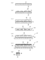
- FIG. 2 is a conceptual cross-sectional view showing a manufacturing process of a fan out type WLP.
- FIG. 2A shows a state in which the adhesive layer 21 is formed on one surface of the support member 20. A peeling layer may be formed between the support member 20 and the adhesive layer 21 as necessary.
- FIG. 2B a plurality of semiconductor chips 22 are pasted on the adhesive layer 21. At that time, the surface on the active side of the semiconductor chip 22 is brought into contact with the adhesive layer 21.
- the semiconductor chip 22 is molded with a resin sealing material 23.
- the sealing material 23 is made of a material having little dimensional change after compression molding and little dimensional change when forming a wiring. Subsequently, as shown in FIGS.
- the processed substrate 24 is cut for each semiconductor chip 22 and used for a subsequent packaging process.
- the supporting glass substrate 26 is reused after being subjected to an acid treatment with HCl or the like (FIG. 2 (g)).
- Tables 1 and 2 show examples of the present invention (sample Nos. 1 to 7, 9 to 22) and comparative examples (sample No. 8).
- Sample no. 1 to 7 were produced. First, as a glass composition, SiO 2 65.6%, Al 2 O 3 8.0%, B 2 O 3 9.1%, Na 2 O 12.8%, CaO 3.2%, ZnO in mass%. Glass raw materials were prepared and mixed so as to contain 0.9%, SnO 2 0.3%, and Sb 2 O 3 0.1% to obtain a glass batch, which was then supplied to a glass melting furnace at 1550 ° C. Then, the obtained molten glass was clarified and stirred, and then supplied to a molding apparatus of an overflow down draw method to form a sheet thickness of 0.7 mm. Thereafter, the obtained glass substrate was cut into a rectangular shape. In addition, when the strain point was measured by the method as described in ASTM C336 about the obtained glass substrate, it was 519 degreeC.
- a heat-treating setter larger than the size of the glass substrate is prepared, and the molded glass substrate is placed on the heat-treating setter, and the heat-resistant substrate is further placed on the glass substrate.
- the temperature inside the electric furnace was raised to the maximum temperature described in the table, and the electric furnace was cooled at the rate of temperature reduction described in the table after being held at the maximum temperature for the time described in the table.
- sample No. Reference numeral 8 denotes a molded glass substrate that has not been subjected to the heat treatment.
- the density of the glass substrate after the heat treatment was measured by the Archimedes method.
- Sample no. 9 and 10 were produced.
- a glass composition by mass%, SiO 2 61.7%, Al 2 O 3 18.0%, B 2 O 3 0.5%, Na 2 O 14.5%, K 2 O 2.0% , MgO 3.0%, SnO 2 0.3% is prepared, mixed and mixed to obtain a glass batch, which is then fed to a glass melting furnace and melted at 1600 ° C.
- the molten glass was clarified and stirred, and then supplied to an overflow down-draw molding apparatus so that the thickness was 1.1 mm. Thereafter, the obtained glass substrate was cut into a rectangular shape. In addition, it was 567 degreeC when the strain point was measured by the method of ASTM C336 about the obtained glass substrate.
- a heat-treating setter larger than the size of the glass substrate is prepared, and the molded glass substrate is placed on the heat-treating setter, and the heat-resistant substrate is further placed on the glass substrate.
- the temperature inside the electric furnace was raised to the maximum temperature described in the table, and the electric furnace was cooled at the rate of temperature reduction described in the table after being held at the maximum temperature for the time described in the table.
- an average linear thermal expansion coefficient in a temperature range of 20 to 220 ° C. and an average linear thermal expansion coefficient in a temperature range of 30 to 380 ° C. were measured with a dilatometer (DIL402C manufactured by Netch Japan).
- the sample No. 9 and 10 can change the thermal expansion coefficient of the glass substrate to a target value by appropriately adjusting the heat treatment conditions.
- Sample no. 11 and 12 were produced. First, by mass%, SiO 2 56.2%, Al 2 O 3 13.0%, B 2 O 3 2.0%, Na 2 O 14.5%, K 2 O 4.9%, MgO 2.
- a glass raw material is prepared and mixed so as to contain 0%, CaO 2.0%, ZrO 2 4.0% SnO 2 0.35%, Sb 2 O 3 0.05%, CeO 2 1.0%. After obtaining a glass batch, it is supplied to a glass melting furnace and melted at 1600 ° C. Then, the obtained molten glass is clarified and stirred, and then supplied to a molding apparatus of an overflow down draw method. Molded to 1 mm. Thereafter, the obtained glass substrate was cut into a rectangular shape. In addition, when the strain point was measured by the method as described in ASTM C336 about the obtained glass substrate, it was 558 degreeC.
- a heat-treating setter larger than the size of the glass substrate is prepared, and the molded glass substrate is placed on the heat-treating setter, and the heat-resistant substrate is further placed on the glass substrate.
- the temperature inside the electric furnace was raised to the maximum temperature described in the table, and the electric furnace was cooled at the rate of temperature reduction described in the table after being held at the maximum temperature for the time described in the table.
- an average linear thermal expansion coefficient in a temperature range of 20 to 220 ° C. and an average linear thermal expansion coefficient in a temperature range of 30 to 380 ° C. were measured with a dilatometer (DIL402C manufactured by Netch Japan).
- the sample No. 11 and 12 can change the thermal expansion coefficient of the glass substrate to a target value by appropriately adjusting the heat treatment conditions.
- Sample no. 13 and 14 were produced. First, by mass%, SiO 2 60.4%, Al 2 O 3 10.7%, Na 2 O 15.5%, K 2 O 8.8%, MgO 1.7%, CaO 2.6%, A glass raw material was prepared and mixed so as to contain 0.3% of Sb 2 O 3 , and a glass batch was obtained. Then, it was supplied to a glass melting furnace and melted at 1400 ° C., and then the obtained molten glass was clarified. After stirring, the mixture was supplied to an overflow down-draw molding apparatus and molded to a thickness of 1.1 mm. Thereafter, the obtained glass substrate was cut into a rectangular shape. In addition, about the obtained glass substrate, when the strain point was measured by the method as described in ASTM C336, it was 452 degreeC.
- a heat-treating setter larger than the size of the glass substrate is prepared, and the molded glass substrate is placed on the heat-treating setter, and the heat-resistant substrate is further placed on the glass substrate.
- the temperature inside the electric furnace was raised to the maximum temperature described in the table, and the electric furnace was cooled at the rate of temperature reduction described in the table after being held at the maximum temperature for the time described in the table.
- an average linear thermal expansion coefficient in a temperature range of 20 to 220 ° C. and an average linear thermal expansion coefficient in a temperature range of 30 to 380 ° C. were measured with a dilatometer (DIL402C manufactured by Netch Japan).
- the sample No. 13 and 14 can change the thermal expansion coefficient of the glass substrate to a target value by appropriately adjusting the heat treatment conditions.
- Sample no. 15 and 16 were produced. First, by mass%, SiO 2 60.4%, Al 2 O 3 8.7%, Na 2 O 13.6%, K 2 O 12.7%, MgO 1.6%, CaO 2.5%, A glass raw material was prepared and mixed so as to contain 0.2% Sb 2 O 3 and 0.3% SnO 2 to obtain a glass batch, which was then supplied to a glass melting furnace and melted at 1350 ° C. The obtained molten glass was clarified and stirred, and then supplied to an overflow down-draw molding apparatus so as to have a thickness of 1.1 mm. Thereafter, the obtained glass substrate was cut into a rectangular shape. In addition, when the strain point was measured about the obtained glass substrate by the method of ASTM C336, it was 445 degreeC.
- a heat-treating setter larger than the size of the glass substrate is prepared, and the molded glass substrate is placed on the heat-treating setter, and the heat-resistant substrate is further placed on the glass substrate.
- the temperature inside the electric furnace was raised to the maximum temperature described in the table, and the electric furnace was cooled at the rate of temperature reduction described in the table after being held at the maximum temperature for the time described in the table.
- an average linear thermal expansion coefficient in a temperature range of 20 to 220 ° C. and an average linear thermal expansion coefficient in a temperature range of 30 to 380 ° C. were measured with a dilatometer (DIL402C manufactured by Netch Japan).
- the sample No. 15 and 16 can change the thermal expansion coefficient of the glass substrate to a target value by appropriately adjusting the heat treatment conditions.
- Sample no. 17 and 18 were produced. First, by mass%, SiO 2 66.1%, Al 2 O 3 8.5%, B 2 O 3 12.4%, Na 2 O 8.4%, CaO 3.3%, ZnO 1.0% The glass raw material was prepared and mixed so as to contain 0.3% of SnO 2 to obtain a glass batch, which was then fed to a glass melting furnace and melted at 1500 ° C., and then the obtained molten glass was clarified, After stirring, the mixture was supplied to an overflow down-draw molding apparatus and molded to a thickness of 1.1 mm. Thereafter, the obtained glass substrate was cut into a rectangular shape. In addition, it was 532 degreeC when the strain point was measured about the obtained glass substrate by the method of ASTMC336.
- a heat-treating setter larger than the size of the glass substrate is prepared, and the molded glass substrate is placed on the heat-treating setter, and the heat-resistant substrate is further placed on the glass substrate.
- the temperature inside the electric furnace was raised to the maximum temperature described in the table, and the electric furnace was cooled at the rate of temperature reduction described in the table after being held at the maximum temperature for the time described in the table.
- an average linear thermal expansion coefficient in a temperature range of 20 to 220 ° C. and an average linear thermal expansion coefficient in a temperature range of 30 to 380 ° C. were measured with a dilatometer (DIL402C manufactured by Netch Japan).
- the sample No. 17 and 18 can change the thermal expansion coefficient of the glass substrate to a target value by appropriately adjusting the heat treatment conditions.
- Sample no. 19 and 20 were produced. First, by mass%, SiO 2 58.1%, Al 2 O 3 13.0%, Li 2 O 0.1%, Na 2 O 14.5%, K 2 O 5.5%, MgO 2.0 %, CaO 2.0%, ZrO 2 4.5%, SnO 2 0.3% are mixed and mixed to obtain a glass batch, and then supplied to a glass melting furnace 1500 After melting at 0 ° C., the obtained molten glass was clarified and stirred, and then supplied to a molding apparatus of an overflow down draw method to form a sheet thickness of 0.7 mm. Thereafter, the obtained glass substrate was cut into a rectangular shape. In addition, it was 517 degreeC when the strain point was measured by the method of ASTM C336 about the obtained glass substrate.
- a heat-treating setter larger than the size of the glass substrate is prepared, and the molded glass substrate is placed on the heat-treating setter, and the heat-resistant substrate is further placed on the glass substrate.
- the temperature inside the electric furnace was raised to the maximum temperature described in the table, and the electric furnace was cooled at the rate of temperature reduction described in the table after being held at the maximum temperature for the time described in the table.
- an average linear thermal expansion coefficient in a temperature range of 20 to 220 ° C. and an average linear thermal expansion coefficient in a temperature range of 30 to 380 ° C. were measured with a dilatometer (DIL402C manufactured by Netch Japan).
- the sample No. Nos. 19 and 20 can change the thermal expansion coefficient of the glass substrate to a target value by appropriately adjusting the heat treatment conditions.
- Sample no. 21 and 22 were produced. First, by mass%, SiO 2 47.5%, Al 2 O 3 23.0%, P 2 O 5 13.1%, Na 2 O 14.7%, MgO 1.5%, SnO 2 0.2.
- the glass raw material is prepared and mixed so as to contain%, and after obtaining a glass batch, it is supplied to a glass melting furnace and melted at 1500 ° C., and then the obtained molten glass is clarified and stirred, and then overflowed.
- the material was supplied to a downdraw molding apparatus and molded so as to have a thickness of 0.7 mm. Thereafter, the obtained glass substrate was cut into a rectangular shape. In addition, it was 595 degreeC when the strain point was measured about the obtained glass substrate by the method of ASTMC336.
- a heat-treating setter larger than the size of the glass substrate is prepared, and the molded glass substrate is placed on the heat-treating setter, and the heat-resistant substrate is further placed on the glass substrate.
- the temperature inside the electric furnace was raised to the maximum temperature described in the table, and the electric furnace was cooled at the rate of temperature reduction described in the table after being held at the maximum temperature for the time described in the table.
- an average linear thermal expansion coefficient in a temperature range of 20 to 220 ° C. and an average linear thermal expansion coefficient in a temperature range of 30 to 380 ° C. were measured with a dilatometer (DIL402C manufactured by Netch Japan).
- the sample No. 21 and 22 can change the thermal expansion coefficient of the glass substrate to a target value by appropriately adjusting the heat treatment conditions.
- various glass substrates after heat treatment were cut out to ⁇ 300 mm, and then both surfaces of the glass substrate were polished by a polishing apparatus. Specifically, both surfaces of the glass substrate were sandwiched between a pair of polishing pads having different outer diameters, and both surfaces of the glass substrate were polished while rotating the glass substrate and the pair of polishing pads together. During the polishing process, control was sometimes performed so that a part of the glass substrate protruded from the polishing pad.
- the polishing pad was made of urethane, the average particle size of the polishing slurry used for the polishing treatment was 2.5 ⁇ m, and the polishing rate was 15 m / min.
- the whole board thickness deviation and curvature amount were measured by Bow / Warp measuring apparatus SBW-331ML / d by Kobelco Kaken. As a result, the overall plate thickness deviation was less than 1.0 ⁇ m, and the warpage amount was 35 ⁇ m or less.
Landscapes
- Chemical & Material Sciences (AREA)
- Engineering & Computer Science (AREA)
- Materials Engineering (AREA)
- Organic Chemistry (AREA)
- Physics & Mathematics (AREA)
- Thermal Sciences (AREA)
- Ceramic Engineering (AREA)
- Mechanical Engineering (AREA)
- Inorganic Chemistry (AREA)
- Container, Conveyance, Adherence, Positioning, Of Wafer (AREA)
- Re-Forming, After-Treatment, Cutting And Transporting Of Glass Products (AREA)
- Surface Treatment Of Glass (AREA)
- Glass Compositions (AREA)
Abstract
Priority Applications (4)
| Application Number | Priority Date | Filing Date | Title |
|---|---|---|---|
| CN201680069435.9A CN108367961A (zh) | 2015-12-17 | 2016-12-07 | 支承玻璃基板的制造方法 |
| JP2017556000A JP6987356B2 (ja) | 2015-12-17 | 2016-12-07 | 支持ガラス基板の製造方法 |
| KR1020187014644A KR102588111B1 (ko) | 2015-12-17 | 2016-12-07 | 지지 유리 기판의 제조 방법 |
| JP2021188397A JP7268718B2 (ja) | 2015-12-17 | 2021-11-19 | 支持ガラス基板の製造方法 |
Applications Claiming Priority (2)
| Application Number | Priority Date | Filing Date | Title |
|---|---|---|---|
| JP2015-246131 | 2015-12-17 | ||
| JP2015246131 | 2015-12-17 |
Publications (1)
| Publication Number | Publication Date |
|---|---|
| WO2017104513A1 true WO2017104513A1 (fr) | 2017-06-22 |
Family
ID=59056471
Family Applications (1)
| Application Number | Title | Priority Date | Filing Date |
|---|---|---|---|
| PCT/JP2016/086427 Ceased WO2017104513A1 (fr) | 2015-12-17 | 2016-12-07 | Procédé de fabrication de substrat de support en verre |
Country Status (5)
| Country | Link |
|---|---|
| JP (2) | JP6987356B2 (fr) |
| KR (1) | KR102588111B1 (fr) |
| CN (1) | CN108367961A (fr) |
| TW (1) | TWI701221B (fr) |
| WO (1) | WO2017104513A1 (fr) |
Cited By (10)
| Publication number | Priority date | Publication date | Assignee | Title |
|---|---|---|---|---|
| CN112437759A (zh) * | 2018-07-16 | 2021-03-02 | 康宁股份有限公司 | 具有改善的翘曲的玻璃制品的陶瓷化方法 |
| KR20210024558A (ko) * | 2018-06-28 | 2021-03-05 | 코닝 인코포레이티드 | 유리 리본을 제조하는 연속적인 방법 및 이로부터 인발된(as-drawn) 유리 물품 |
| US11370693B2 (en) | 2019-01-28 | 2022-06-28 | Corning Incorporated | Glass-ceramic articles, compositions, and methods of making the same |
| US11649187B2 (en) | 2018-07-16 | 2023-05-16 | Corning Incorporated | Glass ceramic articles having improved properties and methods for making the same |
| US11739018B2 (en) | 2019-09-13 | 2023-08-29 | Corning Incorporated | Continuous methods of forming glass ribbon using a gyrotron microwave heating device |
| US11834363B2 (en) | 2018-07-16 | 2023-12-05 | Corning Incorporated | Methods for ceramming glass with nucleation and growth density and viscosity changes |
| US11912605B2 (en) | 2018-06-28 | 2024-02-27 | Corning Incorporated | Glass articles |
| US12071367B2 (en) | 2018-07-16 | 2024-08-27 | Corning Incorporated | Glass substrates including uniform parting agent coatings and methods of ceramming the same |
| US12077464B2 (en) | 2018-07-16 | 2024-09-03 | Corning Incorporated | Setter plates and methods of ceramming glass articles using the same |
| WO2025239392A1 (fr) * | 2024-05-17 | 2025-11-20 | 日本電気硝子株式会社 | Substrat en verre de support, feuilleté, procédé de production de feuilleté, procédé de production d'un boîtier de semi-conducteur, et substrat en verre |
Families Citing this family (1)
| Publication number | Priority date | Publication date | Assignee | Title |
|---|---|---|---|---|
| JP7814673B2 (ja) * | 2020-05-28 | 2026-02-17 | 日本電気硝子株式会社 | 支持ガラス基板及びこれを用いた積層基板 |
Citations (5)
| Publication number | Priority date | Publication date | Assignee | Title |
|---|---|---|---|---|
| WO2013145503A1 (fr) * | 2012-03-29 | 2013-10-03 | コニカミノルタ株式会社 | Procédé de production de substrat en verre pour disques durs |
| WO2015037478A1 (fr) * | 2013-09-12 | 2015-03-19 | 日本電気硝子株式会社 | Substrat de support en verre et élément de transport l'utilisant |
| WO2015156075A1 (fr) * | 2014-04-07 | 2015-10-15 | 日本電気硝子株式会社 | Substrat de support en verre et élément multicouche l'utilisant |
| JP2015224171A (ja) * | 2014-05-29 | 2015-12-14 | 日本電気硝子株式会社 | ガラス基板の製造方法 |
| WO2016111152A1 (fr) * | 2015-01-05 | 2016-07-14 | 日本電気硝子株式会社 | Substrat de soutien en verre et son procédé de fabrication |
Family Cites Families (5)
| Publication number | Priority date | Publication date | Assignee | Title |
|---|---|---|---|---|
| US3505571A (en) * | 1965-09-30 | 1970-04-07 | Gen Electric | Glass covered semiconductor device |
| JP4792705B2 (ja) | 2003-04-03 | 2011-10-12 | 旭硝子株式会社 | TiO2を含有するシリカガラスおよびその製造法 |
| JP5332085B2 (ja) | 2006-06-28 | 2013-11-06 | 日本電気硝子株式会社 | フラットパネルディスプレイ用のガラス基板の製造方法 |
| WO2014073455A1 (fr) * | 2012-11-09 | 2014-05-15 | 日本電気硝子株式会社 | Stratifié de film de verre, et procédé de fabrication de dispositif électronique/électrique |
| WO2016002778A1 (fr) * | 2014-06-30 | 2016-01-07 | AvanStrate株式会社 | Procédé de production d'une feuille de verre et dispositif de production d'une feuille de verre |
-
2016
- 2016-12-07 WO PCT/JP2016/086427 patent/WO2017104513A1/fr not_active Ceased
- 2016-12-07 JP JP2017556000A patent/JP6987356B2/ja active Active
- 2016-12-07 CN CN201680069435.9A patent/CN108367961A/zh active Pending
- 2016-12-07 KR KR1020187014644A patent/KR102588111B1/ko active Active
- 2016-12-08 TW TW105140524A patent/TWI701221B/zh active
-
2021
- 2021-11-19 JP JP2021188397A patent/JP7268718B2/ja active Active
Patent Citations (5)
| Publication number | Priority date | Publication date | Assignee | Title |
|---|---|---|---|---|
| WO2013145503A1 (fr) * | 2012-03-29 | 2013-10-03 | コニカミノルタ株式会社 | Procédé de production de substrat en verre pour disques durs |
| WO2015037478A1 (fr) * | 2013-09-12 | 2015-03-19 | 日本電気硝子株式会社 | Substrat de support en verre et élément de transport l'utilisant |
| WO2015156075A1 (fr) * | 2014-04-07 | 2015-10-15 | 日本電気硝子株式会社 | Substrat de support en verre et élément multicouche l'utilisant |
| JP2015224171A (ja) * | 2014-05-29 | 2015-12-14 | 日本電気硝子株式会社 | ガラス基板の製造方法 |
| WO2016111152A1 (fr) * | 2015-01-05 | 2016-07-14 | 日本電気硝子株式会社 | Substrat de soutien en verre et son procédé de fabrication |
Non-Patent Citations (1)
| Title |
|---|
| SUMIO SAKKA, GLASS NO HYAKKA JITEN, 2007, Tokyo : Asakura Publishing Co., Ltd., pages 578 - 579, ISBN: 978-4-254-20124-6 * |
Cited By (15)
| Publication number | Priority date | Publication date | Assignee | Title |
|---|---|---|---|---|
| KR20210024558A (ko) * | 2018-06-28 | 2021-03-05 | 코닝 인코포레이티드 | 유리 리본을 제조하는 연속적인 방법 및 이로부터 인발된(as-drawn) 유리 물품 |
| JP2021529718A (ja) * | 2018-06-28 | 2021-11-04 | コーニング インコーポレイテッド | ガラスリボンを連続的に製造する方法および同ガラスリボンから製造された延伸済みのガラス物品 |
| KR102743378B1 (ko) * | 2018-06-28 | 2024-12-17 | 코닝 인코포레이티드 | 유리 리본을 제조하는 연속적인 방법 및 이로부터 인발된(as-drawn) 유리 물품 |
| US11912605B2 (en) | 2018-06-28 | 2024-02-27 | Corning Incorporated | Glass articles |
| JP7511487B2 (ja) | 2018-06-28 | 2024-07-05 | コーニング インコーポレイテッド | ガラスリボンを連続的に製造する方法および同ガラスリボンから製造された延伸済みのガラス物品 |
| US12077464B2 (en) | 2018-07-16 | 2024-09-03 | Corning Incorporated | Setter plates and methods of ceramming glass articles using the same |
| CN112437759A (zh) * | 2018-07-16 | 2021-03-02 | 康宁股份有限公司 | 具有改善的翘曲的玻璃制品的陶瓷化方法 |
| US11613491B2 (en) | 2018-07-16 | 2023-03-28 | Corning Incorporated | Methods of ceramming glass articles having improved warp |
| US11649187B2 (en) | 2018-07-16 | 2023-05-16 | Corning Incorporated | Glass ceramic articles having improved properties and methods for making the same |
| US11834363B2 (en) | 2018-07-16 | 2023-12-05 | Corning Incorporated | Methods for ceramming glass with nucleation and growth density and viscosity changes |
| US12071367B2 (en) | 2018-07-16 | 2024-08-27 | Corning Incorporated | Glass substrates including uniform parting agent coatings and methods of ceramming the same |
| US12071364B2 (en) | 2018-07-16 | 2024-08-27 | Corning Incorporated | Glass ceramic articles having improved properties and methods for making the same |
| US11370693B2 (en) | 2019-01-28 | 2022-06-28 | Corning Incorporated | Glass-ceramic articles, compositions, and methods of making the same |
| US11739018B2 (en) | 2019-09-13 | 2023-08-29 | Corning Incorporated | Continuous methods of forming glass ribbon using a gyrotron microwave heating device |
| WO2025239392A1 (fr) * | 2024-05-17 | 2025-11-20 | 日本電気硝子株式会社 | Substrat en verre de support, feuilleté, procédé de production de feuilleté, procédé de production d'un boîtier de semi-conducteur, et substrat en verre |
Also Published As
| Publication number | Publication date |
|---|---|
| JP7268718B2 (ja) | 2023-05-08 |
| JP6987356B2 (ja) | 2021-12-22 |
| KR20180095513A (ko) | 2018-08-27 |
| TW201731783A (zh) | 2017-09-16 |
| JP2022025147A (ja) | 2022-02-09 |
| CN108367961A (zh) | 2018-08-03 |
| KR102588111B1 (ko) | 2023-10-12 |
| JPWO2017104513A1 (ja) | 2018-10-04 |
| TWI701221B (zh) | 2020-08-11 |
Similar Documents
| Publication | Publication Date | Title |
|---|---|---|
| JP7268718B2 (ja) | 支持ガラス基板の製造方法 | |
| JP6611079B2 (ja) | ガラス板 | |
| KR102430746B1 (ko) | 지지 유리 기판 및 그 제조 방법 | |
| JP6741214B2 (ja) | 支持ガラス基板及びこれを用いた積層体 | |
| JP6519221B2 (ja) | ガラス基板及びこれを用いた積層体 | |
| JP6593676B2 (ja) | 積層体及び半導体パッケージの製造方法 | |
| WO2017104514A1 (fr) | Substrat de support en vitrocéramique, et stratifié mettant en œuvre celui-ci | |
| JPWO2016047210A1 (ja) | 支持ガラス基板及びこれを用いた積層体 | |
| JP2016117641A (ja) | 支持ガラス基板及びこれを用いた積層体 | |
| TW201910285A (zh) | 支持玻璃基板及使用此之層積基板 | |
| CN107108318B (zh) | 玻璃板及其制造方法 | |
| JP2016169141A (ja) | 支持ガラス基板及びこれを用いた積層体 | |
| JP2016155736A (ja) | 支持ガラス基板及びこれを用いた積層体 | |
| TWI755449B (zh) | 支撐玻璃基板及使用其的積層體、半導體封裝體及其製造方法以及電子機器 | |
| JP2022161964A (ja) | 支持ガラス基板の製造方法 | |
| JP6813813B2 (ja) | ガラス板 | |
| JP2020172436A (ja) | 支持ガラス基板及びそれを用いた積層体 | |
| WO2016098499A1 (fr) | Substrat support en verre et stratifié l'utilisant |
Legal Events
| Date | Code | Title | Description |
|---|---|---|---|
| 121 | Ep: the epo has been informed by wipo that ep was designated in this application |
Ref document number: 16875493 Country of ref document: EP Kind code of ref document: A1 |
|
| ENP | Entry into the national phase |
Ref document number: 2017556000 Country of ref document: JP Kind code of ref document: A |
|
| ENP | Entry into the national phase |
Ref document number: 20187014644 Country of ref document: KR Kind code of ref document: A |
|
| NENP | Non-entry into the national phase |
Ref country code: DE |
|
| 122 | Ep: pct application non-entry in european phase |
Ref document number: 16875493 Country of ref document: EP Kind code of ref document: A1 |