WO2017104597A1 - Élément fusible - Google Patents
Élément fusible Download PDFInfo
- Publication number
- WO2017104597A1 WO2017104597A1 PCT/JP2016/086857 JP2016086857W WO2017104597A1 WO 2017104597 A1 WO2017104597 A1 WO 2017104597A1 JP 2016086857 W JP2016086857 W JP 2016086857W WO 2017104597 A1 WO2017104597 A1 WO 2017104597A1
- Authority
- WO
- WIPO (PCT)
- Prior art keywords
- heating element
- electrode
- insulating substrate
- electrodes
- fuse element
- Prior art date
- Legal status (The legal status is an assumption and is not a legal conclusion. Google has not performed a legal analysis and makes no representation as to the accuracy of the status listed.)
- Ceased
Links
Images









Classifications
-
- H—ELECTRICITY
- H01—ELECTRIC ELEMENTS
- H01H—ELECTRIC SWITCHES; RELAYS; SELECTORS; EMERGENCY PROTECTIVE DEVICES
- H01H37/00—Thermally-actuated switches
- H01H37/74—Switches in which only the opening movement or only the closing movement of a contact is effected by heating or cooling
- H01H37/76—Contact member actuated by melting of fusible material, actuated due to burning of combustible material or due to explosion of explosive material
Definitions
- the present invention relates to a fuse element that protects a circuit by cutting off a power supply line or a signal line.
- This application is based on Japanese Patent Application No. 2015-247288 filed on December 18, 2015 in Japan and Japanese Application No. 2016-110506 filed on June 1, 2016 in Japan. Priority is claimed and these applications are incorporated herein by reference.
- a fusible conductor is connected between a first electrode formed on an insulating substrate, a heating element lead electrode connected to the heating element, and a second electrode. Then, a circuit is formed by energizing a fusible conductor on the current path that is fused by self-heating due to overcurrent or a heating element provided inside the fuse element by an external signal. There is one that melts the fusible conductor at the timing that the side intends.
- FIG. 30 shows an example of a fuse element.
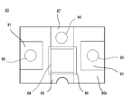
- 30 to 32 is laminated on the insulating substrate 85, the first and second electrodes 81 and 82 formed on both ends of the surface 85a of the insulating substrate 85, and the back surface 85b of the insulating substrate 85 to be insulated.
- the heating element 84 covered with the layer 86, the intermediate electrode 88 laminated on the surface 85a of the insulating substrate 85 and electrically connected to the heating element 84, and both ends of the first and second electrodes 81 and 82, respectively.
- a fusible conductor 83 having a central portion connected to the intermediate electrode 88.
- the first and second electrodes 81 and 82 are connected to the first and second mounting electrodes 91 and 92 provided on the back surface 85 b of the insulating substrate 85 through the through holes 90.
- the heating element 84 has one end connected to the heating element extraction electrode 87 provided on the back surface 85 b of the insulating substrate 85 and the other end connected to the heating element electrode 93 provided on the back surface 85 b of the insulating substrate 85. .
- the heating element extraction electrode 87 is connected to the intermediate electrode 88 through the through hole 94.
- the fusible conductor 83 is made of a material that is quickly melted by the heat generated by the heating element 84, and is made of, for example, low melting point metal such as solder or Pb-free solder containing Sn as a main component.
- the fuse element 80 When an abnormality such as overcharge or overdischarge is detected, the fuse element 80 is energized to the heating element 84 from the heating element electrode 93 connected to an external circuit. In the fuse element 80, the fusible conductor 83 is melted when the heating element 84 generates heat, and the molten conductor is collected in the first and second electrodes 81 and 82 and the intermediate electrode 88, whereby the first and second fuse elements 80 are collected. The current path between the electrodes 81 and 82 is interrupted.
- a heating element 84, a heating element extraction electrode 87, and first and second mounting electrodes 91 and 92 are formed on the back surface 85b of the insulating substrate 85.
- the area where the heating element 84 can be disposed by the first and second mounting electrodes 91 and 92 is narrowed, and the soluble conductor 83 cannot be quickly blown even by energization heat generation.
- the heat generating body 84 itself burns out before the fusible conductor 83 is melted due to local overheating, and the fusible conductor 83 cannot be melted stably.
- the size of the heating element 84 is as small as 0.8 mm ⁇ 0.8 mm.
- the size is limited, making it difficult to handle high current applications.
- the heating element extraction electrode 87 and the first and second mounting electrodes 91 and 92 become small, and the intermediate electrode 88 and the intermediate electrode 88 formed on the surface 85a of the insulating substrate 85 There is insufficient space for conducting electrical continuity with the first and second electrodes 81 and 82 through castellations and through holes.
- the first and second mounting electrodes 91 and 92 become narrow, there is a problem that a connection area to the mounting substrate becomes insufficient, and sufficient connection strength cannot be secured.
- the present invention secures the formation area of the heating element and stably melts the fusible conductor even when the fuse element is downsized, and secures the connection area of the mounting electrode to increase the connection strength with the mounting board.
- An object is to provide a fuse element that can be secured.
- a fuse element according to the present invention includes an insulating substrate, a first electrode and a second electrode formed on a surface of the insulating substrate, and the first and second electrodes.
- a heat generating element formed on the back surface of the insulating substrate, which generates heat when energized and melts the soluble conductor, and a back electrode formed on the back surface of the insulating substrate. The body and the back electrode are superimposed via an insulating layer.
- both the effective area of the heating element and the mounting electrode can be maximized. Therefore, the heat generated by the heating element is also transferred from the electrode superimposed via the insulating layer, so that the fusing of the soluble conductor becomes faster and more stable.
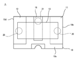
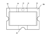
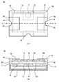
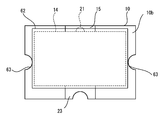
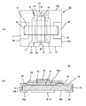
- FIG. 1 is a plan view showing a surface side of an insulating substrate of a fuse element to which the present invention is applied.
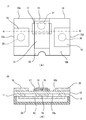
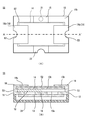
- 2A is a bottom view showing the back side of the insulating substrate of the fuse element to which the present invention is applied
- FIG. 2B is a cross-sectional view taken along the line A-A ′ of FIG.
- FIG. 3 is a circuit diagram showing a configuration example of a battery circuit using a fuse element to which the present invention is applied.
- FIG. 4 is a circuit diagram of a fuse element to which the present invention is applied.
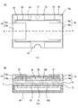
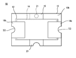
- FIG. 5A is a plan view showing the surface side of an insulating substrate of another fuse element to which the present invention is applied, and FIG.
- FIG. 5B is a cross-sectional view taken along the line A-A ′ of FIG.
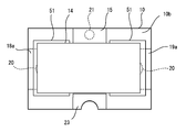
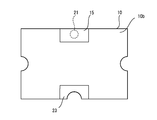
- FIG. 6 is a view showing a manufacturing process of the fuse element shown in FIG. 5, in which a heating element extraction electrode, a lower layer portion of the first and second mounting electrodes, and a heating element electrode are formed on the back surface of the insulating substrate. It is a bottom view which shows the state which formed the 1st insulating layer on it.
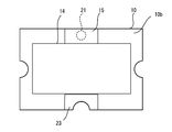
- FIG. 7 is a diagram showing a manufacturing process of the fuse element shown in FIG. 5, and is a bottom view showing a state in which the heating element is superimposed on the lower layer portion by forming the heating element on the first insulating layer. is there.
- FIG. 8 is a view showing a manufacturing process of the fuse element shown in FIG.
- FIG. 5 is a bottom view showing a state in which a second insulating layer is formed on the heating element.
- FIG. 9 is a view showing a manufacturing process of the fuse element shown in FIG. 5 and is a bottom view showing a state in which the upper layer portions of the first and second mounting electrodes are formed on the second insulating layer.
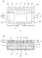
- FIG. 10A is a plan view showing the surface side of an insulating substrate of another fuse element to which the present invention is applied
- FIG. 10B is a cross-sectional view taken along line A-A ′ of FIG.
- FIG. 11 is a view showing a manufacturing process of the fuse element shown in FIG.
- FIG. 10 is a bottom view showing a state in which a heating element extraction electrode and a heating element electrode are formed on the back surface of the insulating substrate.
- FIG. 12 is a view showing a manufacturing process of the fuse element shown in FIG. 10 and is a bottom view showing a state in which a heating element is formed on the back surface of the insulating substrate.
- FIG. 13 is a view showing a manufacturing process of the fuse element shown in FIG. 10 and is a bottom view showing a state in which a second insulating layer is formed on the heating element.
- FIG. 14 is a view showing a manufacturing process of the fuse element shown in FIG. 10, and is a bottom view showing a state in which the upper layer portions of the first and second mounting electrodes are formed on the second insulating layer.
- FIG. 12 is a view showing a manufacturing process of the fuse element shown in FIG. 10 and is a bottom view showing a state in which a heating element is formed on the back surface of the insulating substrate.
- FIG. 13
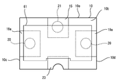
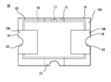
- FIG. 15A is a plan view showing the surface side of an insulating substrate of another fuse element to which the present invention is applied
- FIG. 15B is a cross-sectional view taken along the line A-A ′ of FIG.
- FIG. 16 is a diagram showing a manufacturing process of the fuse element shown in FIG. 15, in which a heating element extraction electrode, lower layers of the first and second mounting electrodes, and a heating element electrode are formed on the back surface of the insulating substrate, and the heating element is formed. It is a bottom view which shows the state which formed the 3rd insulating layer on the extraction electrode and the lower layer part.
- FIG. 17 is a view showing a manufacturing process of the fuse element shown in FIG.
- FIG. 15 is a bottom view showing a state in which a heating element is formed on the third insulating layer.
- FIG. 18 is a view showing a manufacturing process of the fuse element shown in FIG. 15, and is a bottom view showing a state in which a fourth insulating layer is formed on the heating element.
- FIG. 19 is a view showing a manufacturing process of the fuse element shown in FIG. 15, and is a bottom view showing a state in which the upper layer portions of the first and second mounting electrodes are formed on the fourth insulating layer.
- 20A is a plan view showing the surface side of an insulating substrate of another fuse element to which the present invention is applied
- FIG. 20B is a cross-sectional view taken along line A-A ′ of FIG. FIG.
- FIG. 21 is a view showing a manufacturing process of the fuse element shown in FIG. 20, and is a bottom view showing a state in which a heating element extraction electrode heating element electrode is formed on the back surface of the insulating substrate.
- FIG. 22 is a view showing a manufacturing process of the fuse element shown in FIG. 20, and is a bottom view showing a state in which a heating element is formed on the back surface of the insulating substrate.
- FIG. 23 is a view showing a manufacturing process of the fuse element shown in FIG. 20, and is a bottom view showing a state in which a fourth insulating layer is formed on the heating element.
- FIG. 24 is a view showing a manufacturing process of the fuse element shown in FIG.
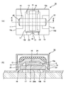
- FIG. 25A is a plan view showing the surface side of the insulating substrate of the fuse element according to the modification with the cap omitted
- FIG. 25B is a cross-sectional view taken along the line AA ′ of FIG.
- FIG. 26 is a cross-sectional view taken along the line B-B ′ of FIG.
- FIG. 27 is a cross-sectional view showing a state of being mounted on an external circuit board.
- FIG. 28 is a plan view showing the surface side of the insulating substrate of the fuse element according to another modification, with the cap omitted.
- FIG. 29A is a plan view showing the surface side of the insulating substrate of the fuse element according to the modified example with the cap omitted
- FIG. 29B is a cross-sectional view taken along the line BB ′ of FIG.
- FIG. 30 is a plan view showing the surface side of the insulating substrate of the fuse element according to the reference example.
- 31 is a cross-sectional view taken along the line A-A ′ of FIG. 30.
- 32 is a bottom view showing the back side of the insulating substrate of the fuse element shown in FIG.
- a fuse element to which the present invention is applied includes an insulating substrate, a first electrode and a second electrode formed on the surface of the insulating substrate, a fusible conductor connected between the first and second electrodes, A heating element that is formed on the back surface of the insulating substrate and that generates heat when energized and melts the fusible conductor, and a back electrode formed on the back surface of the insulating substrate.
- the heating element and the back electrode are overlapped via an insulating layer. ing.
- the back surface electrode superimposed on the heat generating element on the back surface of the insulating substrate is, for example, a heat generating element extraction electrode that is connected to the heat generating element and constitutes an energization path to the heat generating element.
- the back electrode is a first and second mounting electrode connected to the first and second electrodes and mounted on the circuit board.
- the back electrode is a heating element extraction electrode and first and second mounting electrodes.
- the back electrode may be an electrode for heat dissipation or adhesion to a circuit board that is not intended to be energized.
- FIG. 1 and 2 show a fuse element 1 in which a heating element extraction electrode as a back electrode and a heating element are superimposed.
- the fuse element 1 shown in FIG. 1 is formed on the insulating substrate 10, the first electrode 11 and the second electrode 12 formed on the front surface 10a of the insulating substrate 10, the front surface 10a of the insulating substrate 10, and the back surface 10b.
- a first mounting electrode 18 formed on the back surface 10b of the insulating substrate 10 and electrically connected to the first electrode 11 and a second mounting electrode 19 electrically connected to the second electrode 12 are provided. .
- the insulating substrate 10 is formed in a substantially rectangular shape by an insulating member such as alumina, alumina ceramic, glass ceramics, mullite, zirconia.
- the insulating substrate 10 may be made of a material used for a printed wiring board such as a glass epoxy board or a phenol board.
- the fuse element 1 is reduced in size due to demands associated with downsizing of electric devices to be mounted, and the insulating substrate 10 has a size of, for example, 3 mm ⁇ 2 mm and a thickness of 0.3 mm.
- the first and second electrodes 11 and 12 are opened by being spaced apart from each other in the vicinity of opposite side edges on the surface 10a of the insulating substrate 10, and a soluble conductor 13 to be described later is mounted. Thus, they are electrically connected via the soluble conductor 13. Further, the first and second electrodes 11 and 12 generate a large current exceeding the rating through the fuse element 1 and the fusible conductor 13 is melted by self-heating (Joule heat), or the heating element 14 generates heat when energized. The fusible conductor 13 is cut off by fusing.
- the first and second electrodes 11 and 12 are first and second mounting electrodes provided on the back surface 10b through a through hole 20 penetrating the insulating substrate 10, respectively. 18 and 19 are connected.
- the through holes 20 connecting the first and second electrodes 11 and 12 and the first and second mounting electrodes 18 and 19 constitute a part of the energization path of the fuse element 1 and determine the current rating. Therefore, the conductive layer has a predetermined dimension (for example, 0.3 mm ⁇ ) and connects the first electrode 11 and the first mounting electrode 18, and the second electrode 12 and the second mounting electrode 19 inside. Is formed.
- the first and second mounting electrodes 18 and 19 are external connection electrodes that are connected to a circuit board such as a protection circuit on which the fuse element 1 is mounted.
- the first and second mounting electrodes 18 and 19 The second side edges 10c and 10d are separated from each other.
- the fuse element 1 is connected to the circuit board on which an external circuit is formed via the first and second mounting electrodes 18 and 19, and the first mounting electrode 18, the through hole 20, the first electrode 11, A path extending from the molten conductor 13, the second electrode 12, the through hole 20, and the second mounting electrode 19 constitutes a part of the energization path of the external circuit.
- the first and second mounting electrodes 18 and 19 are provided with castellations on the first and second side edges 10c and 10d of the insulating substrate 10 in place of the through holes 20 or together with the through holes 20, and the casters
- the first and second electrodes 11 and 12 may be electrically connected to each other even through the connection.
- the first and second mounting electrodes 18 and 19 secure a connection strength and a predetermined rating by securing a space for conducting through the through hole 20 and the castellation and expanding a connection area to the circuit board. Therefore, a sufficient area is provided, and the resistance of the fuse resistance of the entire element is reduced (for example, 7 m ⁇ ).
- the first and second electrodes 11 and 12 and the first and second mounting electrodes 18 and 19 can be formed using a general electrode material such as Cu or Ag. For example, an Ag—Pd paste is used. It can be formed by printing and baking at 850 ° C. for 30 minutes. Further, on the surfaces of the first and second electrodes 11 and 12 and the first and second mounting electrodes 18 and 19, a coating such as Ni / Au plating, Ni / Pd plating, Ni / Pd / Au plating, or the like is provided on the surfaces of the first and second electrodes 11 and 12 and the first and second mounting electrodes 18 and 19, a coating such as Ni / Au plating, Ni / Pd plating, Ni / Pd / Au plating, or the like is provided. The coating is preferably performed by a known method such as plating.
- the fuse element 1 can prevent the first and second electrodes 11 and 12 and the first and second mounting electrodes 18 and 19 from being oxidized, and can prevent a change in rating due to an increase in conduction resistance. it can. Further, when the fuse element 1 is reflow-mounted, the first and second electrodes 11 and 12 are melted by melting the connecting solder for connecting the fusible conductor 13 or the low melting point metal forming the fusible conductor 13. It is possible to prevent erosion (solder erosion), and the first and second mounting electrodes 18, 18 are obtained by melting the connecting solder for connecting the first and second mounting electrodes to the electrodes of the circuit board. 19 can be prevented from being eroded.
- an intermediate electrode 16 is laminated between the first and second electrodes 11 and 12 on the surface 10 a of the insulating substrate 10.
- the intermediate electrode 16 is connected to the heating element extraction electrode 15 stacked on the back surface 10 b of the insulating substrate 10 through the through hole 21.
- a conductive layer that connects the heating element extraction electrode 15 and the intermediate electrode 16 is formed inside.
- a soluble conductor 13 is connected across the first electrode 11, the intermediate electrode 16, and the second electrode 12.
- the fusible conductor 13 is made of a material that is quickly melted by the heat generated by the heating element 14, and for example, a low melting point metal such as solder or Pb-free solder whose main component is Sn can be suitably used.
- the fusible conductor 13 may be made of a high melting point metal such as In, Pb, Ag, Cu, or an alloy containing any of these as a main component, or the inner layer is a low melting point metal and the outer layer is a high melting point.
- a laminate made of metal may be used.
- the soluble conductor 13 is connected to the intermediate electrode 16 and the first and second electrodes 11 and 12.
- the fusible conductor 13 can be easily connected by reflow soldering.
- solder can be preferably used.
- the soluble conductor 13 is preferably coated with a flux in order to prevent oxidation and improve wettability.
- a heating element 14 On the back surface 10b of the insulating substrate 10, a heating element 14, a heating element extraction electrode 15, first and second mounting electrodes 18 and 19, and a heating element electrode 23 are formed, and the heating element 14 and the heating element extraction are formed.
- the electrode 15 overlaps with the insulating layer 17.
- the heating element extraction electrode 15 is formed on the back surface 10b of the insulating substrate 10 from the third side edge 10e of the insulating substrate toward the center.
- the heating element extraction electrode 15 can be formed by using a general electrode material such as Cu or Ag. For example, it can be formed by printing an Ag—Pd paste and baking at 850 ° C. for 30 minutes. .
- the heating element extraction electrode 15 is connected to one end of the heating element 14 and is connected to the intermediate electrode 16 formed on the surface 10 a of the insulating substrate 10 through the through hole 21.
- the heating element lead-out electrode 15 is provided with a castellation on the third side edge 10e of the insulating substrate 10 instead of the through-hole 21 or together with the through-hole 21, and is electrically connected to the intermediate electrode 16 through the castellation. May be.
- the heating element 14 is a conductive member that generates heat when energized, and is made of, for example, W, Mo, Ru, Cu, Ag, or an alloy containing these as main components.
- the heating element 14 is formed by mixing a powdery body of these alloys, compositions, or compounds with a resin binder, and forming a paste using a screen printing technique, followed by firing (for example, 850 ° C. for 30 minutes). Or the like.
- the resistance value of the patterned heating element 14 is, for example, 1 ⁇ .
- the heating element 14 has one end connected to the heating element extraction electrode 15 and the other end connected to the heating element electrode 23.
- the heating element 14 is connected to an external circuit formed on the circuit board via the heating element electrode 23 by mounting the fuse element 1 on the circuit board.
- the heating element 14 is connected to the first and second electrodes 11 and 12 by being energized and generating heat through a heating element electrode 23 at a predetermined timing to cut off the energization path of the external circuit.
- the molten conductor 13 can be blown.
- the heat generating body 14 also cut
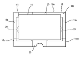
- an insulating layer 17 is disposed so as to cover a part of the heating element extraction electrode 15, and the heating element 14 is superimposed on the heating element extraction electrode 15 via the insulation layer 17.
- the insulating material constituting the insulating layer 17 for example, glass having good heat conduction efficiency can be used.
- the glass paste is printed and baked (for example, 850 ° C. for 30 minutes). can do.
- the heating element 14 is laminated on the back surface 10b and the insulating layer 17 of the insulating substrate 10, and is superimposed on the heating element extraction electrode 15 via the insulating layer 17, thereby generating the heating element extraction electrode. It is connected to a part not covered with 15 insulating layers 17.
- the heating element 14 and the heating element lead-out electrode 15 are overlapped via the insulating layer 17, so that a large space for forming the heating element 14 can be secured in the miniaturized insulating substrate 10. . Therefore, the fuse element 1 can maximize the effective area of the heating element 14, and can melt the soluble conductor 13 quickly and stably. For example, assuming that the size of the insulating substrate is reduced to 3 mm ⁇ 2 mm in the fuse element 1, the size of the heating element 14 can be increased to, for example, 0.8 mm ⁇ 1.2 mm. Of course, the present invention can form a heating element of any size on an insulating substrate of any size.
- the heating element 14 is preferably overlapped with a part or all of the through hole 21 formed in the heating element extraction electrode 15. Since the heating element 14 and the through hole 21 overlap, the heat of the heating element 14 is transmitted to the intermediate electrode 16 and the fusible conductor 13 mounted on the intermediate electrode 16 through the through hole 21 and can be quickly made. The molten conductor 13 can be blown.
- the fuse element 1 may further be provided with a protective layer (not shown) for protecting the heating element 14.
- a protective layer such as glass can be suitably used for the protective layer.
- the fuse element 1 can prevent short-circuiting with peripheral devices and the like, and can prevent wear and damage of the heating element 14 and improve handling.
- the fuse element 1 has a cap 24 for protecting the inside on the surface 10a of the insulating substrate 10. Thereby, the fuse element 1 can prevent the molten soluble conductor 13 from being scattered and can prevent a short circuit with a peripheral device or the like.
- the cap 24 can be formed of a synthetic resin such as nylon or LCP resin (liquid crystal polymer).
- the cap 24 is formed in a size corresponding to the size of the insulating substrate 10 and has a size of, for example, 2.8 ⁇ 1.8 and a thickness of 0.5 mm.
- fuse element 1 is used by being incorporated in a circuit in a battery pack 30 of a lithium ion secondary battery, for example.
- the battery pack 30 has a battery stack 35 including battery cells 31 to 34 of a total of four lithium ion secondary batteries, for example.
- the battery pack 30 includes a battery stack 35, a charge / discharge control circuit 40 that controls charging / discharging of the battery stack 35, a fuse element 1 to which the present invention that cuts off charging when the battery stack 35 is abnormal, and each battery cell A detection circuit 36 for detecting voltages 31 to 34 and a current control element 37 for controlling the operation of the fuse element 1 according to the detection result of the detection circuit 36 are provided.
- the battery stack 35 is a series of battery cells 31 to 34 that need to be controlled to protect against overcharge and overdischarge states, and is detachable via the positive terminal 30a and the negative terminal 30b of the battery pack 30.
- the electronic device can be operated by connecting the positive electrode terminal 30a and the negative electrode terminal 30b of the battery pack 30 charged by the charging device 45 to an electronic device operating with a battery.
- the charge / discharge control circuit 40 includes two current control elements 41 and 42 connected in series to a current path flowing from the battery stack 35 to the charging device 45, and a control unit 43 that controls the operation of these current control elements 41 and 42. Is provided.
- the current control elements 41 and 42 are configured by, for example, field effect transistors (hereinafter referred to as FETs), and the gate voltage is controlled by the control unit 43, whereby the charging direction and / or the discharging direction of the current path of the battery stack 35. Controls continuity and shut-off.
- the control unit 43 operates by receiving power supply from the charging device 45, and controls the current so as to cut off the current path when the battery stack 35 is overdischarged or overcharged according to the detection result by the detection circuit 36. The operation of the elements 41 and 42 is controlled.
- the fuse element 1 is connected, for example, on a charge / discharge current path between the battery stack 35 and the charge / discharge control circuit 40, and its operation is controlled by the current control element 37.
- the detection circuit 36 is connected to the battery cells 31 to 34, detects the voltage values of the battery cells 31 to 34, and supplies the voltage values to the control unit 43 of the charge / discharge control circuit 40.
- the detection circuit 36 outputs a control signal for controlling the current control element 37 when any one of the battery cells 31 to 34 becomes an overcharge voltage or an overdischarge voltage.
- the current control element 37 is composed of, for example, an FET, and when the voltage value of the battery cells 31 to 34 exceeds a predetermined overdischarge or overcharge state by the detection signal output from the detection circuit 36, the fuse element 1 is operated to control the charge / discharge current path of the battery stack 35 to be cut off regardless of the switching operation of the current control elements 41 and 42.
- the fuse element 1 to which the present invention is applied has a circuit configuration as shown in FIG. That is, the fuse element 1 is fusible by generating heat by energizing the fusible conductor 13 connected in series via the intermediate electrode 16 and the heating element lead-out electrode 15, the intermediate electrode 16 and the fusible conductor 13.
- the circuit configuration includes a heating element 14 that melts the conductor 13.
- the fusible conductor 13 is connected in series on the charge / discharge current path, and the heating element 14 is connected to the current control element 37 via the heating element electrode 23.
- the two electrodes 11, 12 of the fuse element 1 one is connected to one open end of the battery stack 35, and the other is connected to the positive electrode terminal 30 a side of the battery pack 30.
- the fuse element 1 having such a circuit configuration can reliably cut off the current path by fusing the fusible conductor 13 by the heat generated by the heating element 14.
- the protection element of the present invention is not limited to use in a battery pack of a lithium ion secondary battery, and can of course be applied to various uses that require interruption of a current path by an electric signal.
- the fuse element to which the present invention is applied the first and second mounting electrodes, which are back electrodes, and the heating element may be overlapped.
- the same members as those of the above-described fuse element 1 are denoted by the same reference numerals, and the details thereof are omitted.
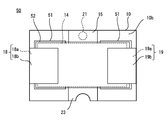
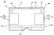
- the heating element 14 and the first and second mounting electrodes 18 and 19 are overlapped via the first and second insulating layers 51 and 52. This is different from the fuse element 1 in that respect.
- the first and second mounting electrodes 18 and 19 in the fuse element 50 are respectively provided in lower layer portions 18a and 19a stacked on the back surface 10b of the insulating substrate 10 and upper layer portions 18b and 19b stacked on the second insulating layer 52. And have.
- the lower layer portions 18a and 19a are formed on the back surface 10b of the insulating substrate 10 so as to be spaced apart from the first and second side edges 10c and 10d of the insulating substrate 10.
- the lower layer portions 18a and 19a can be formed using a general electrode material such as Cu or Ag.
- the lower layer portions 18a and 19a can be formed by printing an Ag—Pd paste and baking at 850 ° C. for 30 minutes.
- the lower layer portions 18 a and 19 a are connected to the first and second electrodes 11 and 12 through the through holes 20 penetrating the insulating substrate 10, respectively.
- the lower layer portions 18a and 19a are covered with the first insulating layer 51 except for a part of the insulating substrate 10 on the first and second side edges 10c and 10d side.
- the insulating material constituting the first insulating layer 51 for example, glass having good heat conduction efficiency can be used, and it can be formed by printing and baking (for example, 850 ° C. for 30 minutes) a glass paste.
- the lower layer portions 18 a and 19 a of the first and second mounting electrodes 18 and 19 and the heating element 14 are overlapped via the first insulating layer 51.
- the heating element 14 is laminated on the back surface 10 b of the insulating substrate 10 and is connected to the heating element extraction electrode 15 and the heating element electrode 23 formed on the back surface 10 b of the insulating substrate 10.
- the heating element 14 has a second insulating layer 52 laminated thereon.
- the second insulating layer 52 has an area equal to or larger than the area of the heating element 14 and covers the entire heating element 14.
- the insulating material constituting the second insulating layer 52 for example, glass having good heat conduction efficiency can be used, and it can be formed by printing and baking (for example, 850 ° C. for 30 minutes) a glass paste.
- the upper layer portions 18 b and 19 b of the first and second mounting electrodes 18 and 19 are superimposed on the heating element 14 via the second insulating layer 52.
- the heating element 14 is superimposed on the lower layer portions 18a and 19a and the upper layer portions 18b and 19b of the first and second mounting electrodes 18 and 19 through the first and second insulating layers 51 and 52, thereby Insulated from the first and second mounting electrodes 18 and 19.
- the upper layer portions 18 b and 19 b are connected to the lower layer portions 18 a and 19 a exposed from the first insulating layer 51.
- the upper layer portions 18b and 19b are external connection electrodes connected to a circuit board such as a protection circuit on which the fuse element 50 is mounted.
- the fuse element 50 is connected to a circuit board on which an external circuit is formed via the upper layer portions 18b and 19b of the first and second mounting electrodes 18 and 19, and the upper layer portion 18b, the lower layer portion 18a, the through hole 20,
- the path extending from the first electrode 11, the fusible conductor 13, the second electrode 12, the through hole 20, the lower layer part 19a, and the upper layer part 19b constitutes a part of the energization path of the external circuit.
- the heating element 14 and the upper and lower layer portions 18a, 18b, 19a, 19b of the first and second mounting electrodes 18, 19 are interposed via the first and second insulating layers 51, 52.
- the fuse element 50 can maximize the effective area of the heating element 14, and can melt the soluble conductor 13 quickly and stably.
- the fuse element 50 can secure a sufficient area of the upper layer portions 18b and 19b of the first and second mounting electrodes 18 and 19, and the mounting area on the circuit board can be maximized to increase the connection strength and A predetermined rating can be provided.
- the heat generating body 14 overlaps with a part or all of the through holes 20 formed in the lower layer portions 18a and 19a. Since the heating element 14 and the through hole 20 overlap each other, the heat of the heating element 14 can be applied to the first and second electrodes 11 and 12 and the first and second electrodes 11 and 12 through the through hole 20.
- the fusible conductor 13 is transmitted to the mounted fusible conductor 13 and can be blown out quickly.
- the lower layer portions 18 a and 19 a of the first and second mounting electrodes 18 and 19 are cast on the first and second side edges 10 c and 10 d of the insulating substrate 10 in place of the through hole 20 or together with the through hole 20.
- the first and second electrodes 11 and 12 may be conducted through the castellation.
- the first insulating layer 51 is provided in each of the lower layer portions 18 a and 19 a as shown in FIG. 5B, and the heating element 14 is overlapped between the first insulating layers 51.
- one first insulating layer 51 may be provided between the lower layer portions 18 a and 19 a so that the entire heating element 14 is formed on the first insulating layer 51.
- Such a fuse element 50 can be manufactured by the steps shown in FIGS. First, as shown in FIG. 6, the heating element extraction electrode 15, the lower layer portions 18 a and 19 a of the first and second mounting electrodes 18 and 19, and the heating element electrode 23 are formed on the back surface 10 b of the insulating substrate 10. Next, the first insulating layer 51 is formed on the lower layer portions 18a and 19a except for a part of the insulating substrate 10 on the first and second side edges 10c and 10d side.
- a heating element 14 is formed.
- the heating element 14 is formed on the first insulating layer 51 so as to overlap the lower layer portions 18a and 19a.
- the heating element 14 is connected to the heating element extraction electrode 15 and the heating element electrode 23.
- a second insulating layer 52 is formed on the heating element 14.
- the second insulating layer 52 covers the entire heating element 14 and exposes the lower layer portions 18a and 19a except for a part of the insulating substrate 10 on the first and second side edges 10c and 10d side. .
- the upper layer portions 18 b and 19 b of the first and second mounting electrodes 18 and 19 are formed on the second insulating layer 52.
- the upper layer portions 18b and 19b are connected to the lower layer portions 18a and 19a at a part of the insulating substrate 10 on the first and second side edges 10c and 10d side.
- the fuse element does not include the lower layer portions 18a and 19a of the first and second mounting electrodes 18 and 19, and the first and second via the castellation 53.
- the two electrodes 11 and 12 may be connected to the upper layer portions 18b and 19b.
- the fuse element 55 shown in FIG. 10 is different from the fuse element 50 in that the lower layer portions 18a and 19a of the first and second mounting electrodes 18 and 19 are not provided. In this case, it is not necessary to provide the first insulating layer 51 that insulates the heating element 14 and the lower layer portions 18a and 19a, but an insulating layer is provided between the back surface 10b of the insulating substrate 10 and the heating element 14. Also good.
- Such a fuse element 55 can be manufactured by the steps shown in FIGS. First, as shown in FIG. 11, the heating element extraction electrode 15 and the heating element electrode 23 are formed on the back surface 10 b of the insulating substrate 10. Next, as shown in FIG. 12, a heating element 14 is formed. The heating element 14 is connected to the heating element extraction electrode 15 and the heating element electrode 23.
- a second insulating layer 52 is formed on the heating element 14.
- the second insulating layer 52 covers the entire heating element 14.
- the upper layer portions 18 b and 19 b of the first and second mounting electrodes 18 and 19 are formed on the second insulating layer 52.
- the upper layer portions 18b and 19b are formed by first and second electrodes formed on the surface 10a of the insulating substrate 10 through castellations 53 formed on the first and second side edges 10c and 10d of the insulating substrate 10, respectively. 11 and 12 are connected.
- the heating element extraction electrode as the back electrode and the first and second mounting electrodes may be overlapped with the heating element.
- the fuse element 60 described below the same members as those of the fuse element 1 and the fuse element 50 described above are denoted by the same reference numerals, and the details thereof are omitted.
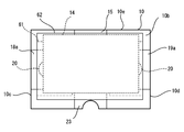
- the heating element 14 and the heating element lead-out electrode 15 are overlapped via a third insulating layer 61, and the heating element 14 and the first and second mounting electrodes are overlapped.
- 18 and 19 are different from the fuse element 1 in that they are superimposed via third and fourth insulating layers 61 and 62.
- the first and second mounting electrodes 18 and 19 in the fuse element 60 are respectively provided in lower layer portions 18a and 19a stacked on the back surface 10b of the insulating substrate 10 and upper layer portions 18b and 19b stacked on the fourth insulating layer 62. And have.
- the third insulating layer 61 is laminated on the heating element extraction electrode 15 and the lower layer portions 18a and 19a.
- the heating element extraction electrode 15 is covered with the third insulating layer 61 except for a part of the insulating substrate 10 on the third side edge 10e side, and the lower layer portions 18a and 19a are formed on the first and second layers of the insulating substrate 10.
- 2 is covered with the third insulating layer 61 except for a part on the side surfaces 10c, 10d side.
- the insulating material constituting the third insulating layer 61 for example, glass having high heat conduction efficiency can be used, and it can be formed by printing and baking (for example, 850 ° C. for 30 minutes) a glass paste.
- the heating element 14 and the lower layer portions 18 a and 19 a of the first and second mounting electrodes 18 and 19 are superimposed on the heating element 14 via the third insulating layer 61. .
- the heating element 14 is laminated on the third insulating layer 61, and the heating element extraction electrode 15 not covered with the third insulating layer 61 and the heating element electrode 23 formed on the back surface 10b of the insulating substrate 10; It is connected.
- the heating element 14 has a fourth insulating layer 62 laminated thereon.
- the fourth insulating layer 62 prevents a short circuit between the heating element 14 and the first and second mounting electrodes 18 and 19, and at least the upper layer portions 18 b and 18 b of the first and second mounting electrodes 18 and 19.
- the heating element 14 on the region where 19b is formed is covered, and preferably the entire heating element 14 is covered.
- As an insulating material constituting the fourth insulating layer 62 for example, glass having high heat conduction efficiency can be used, and it can be formed by printing and baking (for example, 850 ° C. for 30 minutes) a glass paste.
- the upper layer portions 18 b and 19 b of the first and second mounting electrodes 18 and 19 are superimposed on the heating element 14 through the fourth insulating layer 62.
- the heating element 14 is superimposed on the lower layer portions 18a and 19a and the upper layer portions 18b and 19b of the first and second mounting electrodes 18 and 19 through the third and fourth insulating layers 61 and 62, thereby The first and second mounting electrodes 18 and 19 are superposed in an insulated state.
- the upper layer portions 18 b and 19 b are connected to the lower layer portions 18 a and 19 a exposed from the third insulating layer 61.
- the upper layer portions 18b and 19b are external connection electrodes connected to a circuit board such as a protection circuit on which the fuse element 60 is mounted.
- the fuse element 60 is connected to a circuit board on which an external circuit is formed via the upper layer portions 18b and 19b of the first and second mounting electrodes 18 and 19, and the upper layer portion 18b, the lower layer portion 18a, the through hole 20,
- the path extending from the first electrode 11, the fusible conductor 13, the second electrode 12, the through hole 20, the lower layer part 19a, and the upper layer part 19b constitutes a part of the energization path of the external circuit.
- the heating element 14 and the heating element lead-out electrode 15 are overlapped via the third insulating layer 61, and the upper and lower layer portions 18ab, 19ab of the first and second mounting electrodes 18, 19 are overlapped.
- the fuse element 60 can maximize the effective area of the heating element 14, and can melt the soluble conductor 13 quickly and stably.
- the size of the heating element 14 can be increased to, for example, 2.5 mm ⁇ 1.4 mm.
- the fuse element 60 can secure a sufficient area of the upper layer portions 18b and 19b of the first and second mounting electrodes 18 and 19, and maximizes the mounting area on the circuit board, A predetermined rating can be provided.
- the heat generating body 14 is overlapped with a part or all of the through holes 20 and 21 formed in the heat generating body extraction electrode 15 and the lower layer portions 18a and 19a. Since the heating element 14 and the through holes 20 and 21 are overlapped, the first and second electrodes 11 and 12, the intermediate electrode 16, and the first and second electrodes can be heated even when the heat of the heating element 14 passes through the through holes 20 and 21. It is transmitted to the soluble conductor 13 mounted on the two electrodes 11 and 12 and the intermediate electrode 16, and the soluble conductor 13 can be blown out quickly.
- heating element lead-out electrode 15 and the lower layer portions 18a and 19a of the first and second mounting electrodes 18 and 19 are replaced with the through holes 20 and 21 or together with the through holes 20 and 21 with the first through A castellation may be provided on the third side edges 10c to 10e, and the first and second electrodes 11, 12 and the intermediate electrode 16 may be electrically connected through the castellation.
- Such a fuse element 60 can be manufactured by the steps shown in FIGS. First, as shown in FIG. 16, the heating element extraction electrode 15, the lower layer portions 18 a and 19 a of the first and second mounting electrodes 18 and 19, and the heating element electrode 23 are formed on the back surface 10 b of the insulating substrate 10. Next, a part on the first and second side edges 10c and 10d side of the insulating substrate 10 on the lower layer portions 18a and 19a and a part on the third side edge 10e side of the insulating substrate 10 on the heating element extraction electrode 15 A third insulating layer 61 is formed except for.
- a heating element 14 is formed.
- the heating element 14 is formed on the third insulating layer 61 so as to overlap the heating element extraction electrode 15 and the lower layer portions 18a and 19a.
- the heating element 14 is connected to a part of the heating element extraction electrode 15 and the heating element electrode 23 that are not covered with the third insulating layer 61.
- a fourth insulating layer 62 is formed on the heating element 14.
- the fourth insulating layer 62 covers the entire heating element 14 and exposes the lower layer portions 18a and 19a except for a part of the insulating substrate 10 on the first and second side edges 10c and 10d side. .
- upper layer portions 18 b and 19 b of the first and second mounting electrodes 18 and 19 are formed on the fourth insulating layer 62.
- the upper layer portions 18b and 19b are connected to the lower layer portions 18a and 19a at a part of the insulating substrate 10 on the first and second side edges 10c and 10d side.
- the fuse element is not provided with the lower layer portions 18a and 19a of the first and second mounting electrodes 18 and 19, and the first and second via the castellation 63.
- the two electrodes 11 and 12 may be connected to the upper layer portions 18b and 19b.
- the fuse element 65 shown in FIG. 20 is different from the fuse element 60 in that the lower layer portions 18a and 19a of the first and second mounting electrodes 18 and 19 are not provided. In this case, it is not necessary to provide the third insulating layer 61 that insulates the heating element 14 from the lower layer portions 18a and 19a, but an insulating layer is provided between the back surface 10b of the insulating substrate 10 and the heating element 14. Also good.
- Such a fuse element 65 can be manufactured by the steps shown in FIGS. First, as shown in FIG. 21, the heating element extraction electrode 15 and the heating element electrode 23 are formed on the back surface 10 b of the insulating substrate 10. Next, as shown in FIG. 22, the heating element 14 is formed. The heating element 14 is connected to the heating element extraction electrode 15 and the heating element electrode 23.
- a fourth insulating layer 62 is formed on the heating element 14.
- the fourth insulating layer 62 covers the entire heating element 14.
- the upper layer portions 18 b and 19 b of the first and second mounting electrodes 18 and 19 are formed on the fourth insulating layer 62.
- the upper layer portions 18b and 19b are formed by first and second electrodes formed on the surface 10a of the insulating substrate 10 through castellations 63 formed on the first and second side edges 10c and 10d of the insulating substrate 10, respectively. 11 and 12 are connected.
- the first and second electrodes 11 and 12 are provided on the back surface 10b through the through holes 20 penetrating the insulating substrate 10, respectively.
- the first and second mounting electrodes 18 and 19 are connected.
- the first and second electrodes 11 and 12 and the through hole 20 connecting the first and second mounting electrodes 18 and 19 constitute a part of the energization path of the fuse elements 1, 50 and 60, and have a current rating. Therefore, the first electrode 11 and the first mounting electrode 18, and the second electrode 12 and the second mounting electrode 19 are provided therein.
- a conductive layer to be connected is formed.
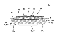
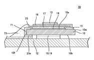
- FIG. 70 In addition to the fuse elements 1, 50 and 60 in which the heating element 14 is formed on the back surface of the insulating substrate 10 as a fuse element in which the conductive through hole 20 in which the conductive layer is formed is formed, FIG. As shown in FIG. 26, the present invention can also be applied to a fuse element 70 in which a heating element is formed on the surface of an insulating substrate.
- the same members as those of the above-described fuse elements 1, 50, 60 are denoted by the same reference numerals, and the details thereof are omitted.
- the fuse element 70 includes the insulating substrate 10, the heating element 14 laminated on the insulating substrate 10 and covered with the insulating layer 17, and the first electrode 11 and the second electrode 12 formed on both ends of the insulating substrate 10.
- the first and second electrodes 11 and 12 are connected to the first and second mounting electrodes 18 and 19 which are external connection electrodes provided on the back surface 10b through the through holes 20 penetrating the insulating substrate 10, respectively.
- the first and second electrodes 11 and 12 and the through hole 20 connecting the first and second mounting electrodes 18 and 19 constitute a part of the energization path of the fuse element 70 and are elements that determine the current rating. Therefore, the conductive layer has a predetermined dimension (for example, 0.3 mm ⁇ ) and connects the first electrode 11 and the first mounting electrode 18, and the second electrode 12 and the second mounting electrode 19 inside. Is formed.
- the heating element 14 can be formed by forming a pattern on the surface 10a of the insulating substrate 10 using a screen printing technique and baking it.
- the heating element 14 has one end connected to the heating element extraction electrode 15 and the other end connected to the heating element electrode 23.
- an insulating layer 17 is disposed so as to cover the heating element 14, and an intermediate electrode 16 is formed so as to face the heating element 14 through the insulating layer 17.
- an insulating layer 17 may be laminated between the heating element 14 and the insulating substrate 10.
- One end of the intermediate electrode 16 is connected to a part of the heating element extraction electrode 15 exposed from the insulating layer 17 and is connected to one end of the heating element 14 via the heating element extraction electrode 15.
- the heating element extraction electrode 15 is formed on the third side surface 10 e side of the insulating substrate 10, and the heating element electrode 23 is formed on the fourth side surface 10 f side of the insulating substrate 10.
- the heating element electrode 23 is connected to an external connection electrode 23a formed on the back surface 10b of the insulating substrate 10 via a castellation 71 formed on the fourth side surface 10f.
- the heating element 14 is connected to an external circuit formed on the circuit board 2 through the external connection electrode 23a by mounting the fuse element 70 on the circuit board 2.
- the heating element 14 can be connected to the first and second electrodes 11 and 12 by being energized through the external connection electrode 23a at a predetermined timing for cutting off the energization path of the external circuit and generating heat.
- the molten conductor 13 can be blown.
- the heat generating body 14 also cut
- a cap 24 that protects the inside is mounted on the surface 10 a of the insulating substrate 10.
- the first and second electrodes 11 and 12 are connected to the first and second mounting electrodes 18 and 19 via the conductive through holes 20, respectively.
- the thickness of the conductive layer can be sufficiently ensured as compared with the case of connection through a conventional castellation, and the first and second electrodes 11 and 12 and the first and second mounting electrodes 18 and 18 can be secured. It is possible to reduce the resistance of the current-carrying path with respect to 19. Therefore, the fuse element 70 can be used for a large current application without the current conduction path hindering the improvement of the rating.
- the heating element electrode 23 serving as an energization path to the heating element 14 is connected to the external connection electrode 23 a formed on the back surface 10 b of the insulating substrate 10 through the castellation 71.
- the fillet 73 is formed in the castellation 71, so that the external connection electrode 23a is surface-connected.
- the mounting strength on the external circuit board 72 can be improved. Further, in the process of mounting the fuse element 70 on the external circuit board 72, by confirming the fillet 73, it is possible to easily determine that the fuse element 70 is securely connected by visual inspection or image inspection.
- the current-carrying path between the heating element electrode 23 and the external connection electrode 23a is formed by the castellation 71, so that the heating element electrode 23 can be made narrower than when the conductive through hole is formed. As a result, the entire device can be reduced in size.
- the fuse element 70 may connect the heating element electrode 23 and the external connection electrode 23a via a side electrode formed on the side surface of the insulating substrate 10 by printing or the like. Also in this case, as in the case of connection via the castellation 71, the connection strength can be improved by forming the fillet 73, and the connection can be easily confirmed. Furthermore, the heating element electrode 23 can be narrowed compared to the case where the conductive through hole is formed, and the entire element can be reduced in size.
- the energization path to the heating element 14 is not an element that determines the rating of the fuse element 70 unlike the energization path of the fusible conductor 13, it may have a higher resistance than the energization path of the fusible conductor 13 (for example, (Several ⁇ order). Therefore, the fuse element 70 does not impair the improvement in rating even when the castellation 71 or the side electrode is used.
- the formation of the castellation 71 has a higher mounting strength, and the manufacturing process is simpler and more advantageous in terms of manufacturing cost, as compared with the case where the side electrode is formed on the side surface of the insulating substrate 10 by printing or the like. .
- the heating element electrode 23 and the external connection electrode 23a have a minimum necessary area. Therefore, it is easy to reduce the size.
- a castellation 74 may be further formed on the first and second electrodes 11 and 12, depending on conditions such as a request for downsizing and a manufacturing cost.
- the first and second electrodes 11 and 12 are provided with a castellation 74 in addition to the conductive through hole 20, thereby further reducing the conduction resistance and improving the mounting strength by forming a fillet.
- confirmation of mounting on the external circuit board 72 can be easily performed by confirming the fillet.
- the fuse element 70 has the first and second electrodes 11 and 12 and the heating element 14 on the surface 10a of the insulating substrate 10 in order to improve the mounting strength to the external circuit board 72.
- the first independent terminal 75 that does not participate in the conduction of the first insulating terminal 75 is provided, and the second independent terminal 76 that does not participate in the conduction with the first and second electrodes 11 and 12 and the heating element 14 is provided on the back surface 10b of the insulating substrate 10.
- the first and second independent terminals 75 and 76 may be connected via a castellation 77.
- the fuse element 70 has a mounting strength to the external circuit board 72. Can be improved.
- the first and second independent terminals 75 and 76 may be connected by a side electrode provided on the side surface of the insulating substrate, and a fillet may be formed along the side electrode.
Landscapes
- Chemical & Material Sciences (AREA)
- Engineering & Computer Science (AREA)
- Combustion & Propulsion (AREA)
- Fuses (AREA)
Abstract
Selon la présente invention, même lorsque la taille d'un élément fusible est réduite, une région de formation d'un corps chauffant est procurée, un conducteur soluble est porté à fusion de manière stable, et une zone de liaison d'une électrode de montage est procurée afin de garantir la résistance de liaison du substrat de montage. La présente invention comporte : un substrat isolant (10) ; une première électrode (11) et une seconde électrode (12) formées sur une surface (10a) du substrat isolant (10) ; un conducteur soluble (13) par l'intermédiaire duquel les première et seconde électrodes (11, 12) sont connectées ; un corps chauffant (14) qui est formé sur la surface arrière (10b) du substrat isolant (10), et qui génère de la chaleur sous l'effet d'un courant électrique le traversant, de manière à porter à fusion le conducteur soluble (13) ; et une électrode de surface arrière (15) formée sur la surface arrière (10b) du substrat isolant (10), le corps chauffant (14) et l'électrode de surface arrière (15) se chevauchant, et une couche isolante (17) étant intercalée entre ces derniers.
Priority Applications (2)
| Application Number | Priority Date | Filing Date | Title |
|---|---|---|---|
| CN201680071024.3A CN108475602B (zh) | 2015-12-18 | 2016-12-12 | 熔丝元件 |
| KR1020187015039A KR102099799B1 (ko) | 2015-12-18 | 2016-12-12 | 퓨즈 소자 |
Applications Claiming Priority (4)
| Application Number | Priority Date | Filing Date | Title |
|---|---|---|---|
| JP2015-247288 | 2015-12-18 | ||
| JP2015247288 | 2015-12-18 | ||
| JP2016110506A JP6797565B2 (ja) | 2015-12-18 | 2016-06-01 | ヒューズ素子 |
| JP2016-110506 | 2016-06-01 |
Publications (1)
| Publication Number | Publication Date |
|---|---|
| WO2017104597A1 true WO2017104597A1 (fr) | 2017-06-22 |
Family
ID=59056630
Family Applications (1)
| Application Number | Title | Priority Date | Filing Date |
|---|---|---|---|
| PCT/JP2016/086857 Ceased WO2017104597A1 (fr) | 2015-12-18 | 2016-12-12 | Élément fusible |
Country Status (1)
| Country | Link |
|---|---|
| WO (1) | WO2017104597A1 (fr) |
Cited By (2)
| Publication number | Priority date | Publication date | Assignee | Title |
|---|---|---|---|---|
| WO2023038078A1 (fr) * | 2021-09-10 | 2023-03-16 | デクセリアルズ株式会社 | Élément de protection et batterie |
| WO2023167069A1 (fr) * | 2022-03-02 | 2023-09-07 | デクセリアルズ株式会社 | Élément de protection |
Citations (2)
| Publication number | Priority date | Publication date | Assignee | Title |
|---|---|---|---|---|
| JPS5947953U (ja) * | 1982-09-22 | 1984-03-30 | 内橋金属工業株式会社 | 過電流保護素子 |
| JP2015053260A (ja) * | 2013-08-07 | 2015-03-19 | デクセリアルズ株式会社 | 保護素子及びバッテリパック |
-
2016
- 2016-12-12 WO PCT/JP2016/086857 patent/WO2017104597A1/fr not_active Ceased
Patent Citations (2)
| Publication number | Priority date | Publication date | Assignee | Title |
|---|---|---|---|---|
| JPS5947953U (ja) * | 1982-09-22 | 1984-03-30 | 内橋金属工業株式会社 | 過電流保護素子 |
| JP2015053260A (ja) * | 2013-08-07 | 2015-03-19 | デクセリアルズ株式会社 | 保護素子及びバッテリパック |
Cited By (5)
| Publication number | Priority date | Publication date | Assignee | Title |
|---|---|---|---|---|
| WO2023038078A1 (fr) * | 2021-09-10 | 2023-03-16 | デクセリアルズ株式会社 | Élément de protection et batterie |
| JP2023040957A (ja) * | 2021-09-10 | 2023-03-23 | デクセリアルズ株式会社 | 保護素子及びバッテリパック |
| JP7841862B2 (ja) | 2021-09-10 | 2026-04-07 | デクセリアルズ株式会社 | 保護素子及びバッテリパック |
| WO2023167069A1 (fr) * | 2022-03-02 | 2023-09-07 | デクセリアルズ株式会社 | Élément de protection |
| JP2023127740A (ja) * | 2022-03-02 | 2023-09-14 | デクセリアルズ株式会社 | 保護素子 |
Similar Documents
| Publication | Publication Date | Title |
|---|---|---|
| JP6797565B2 (ja) | ヒューズ素子 | |
| JP6249602B2 (ja) | 保護素子 | |
| JP6437253B2 (ja) | 保護素子及び実装体 | |
| JP6621255B2 (ja) | 保護素子、ヒューズ素子 | |
| WO2015020111A1 (fr) | Élément protecteur et bloc-batterie | |
| WO2020129406A1 (fr) | Élément de protection et bloc-batterie | |
| WO2013146889A1 (fr) | Élément de protection | |
| JP6957246B2 (ja) | 保護素子 | |
| WO2016117578A1 (fr) | Élément fusible et module de circuit | |
| JP2016035816A (ja) | 保護素子及び保護回路 | |
| CN104508783A (zh) | 保护元件及电池组 | |
| WO2018110154A1 (fr) | Élément de protection | |
| WO2018088308A1 (fr) | Élément de protection | |
| WO2017141678A1 (fr) | Élément fusible | |
| JP6058476B2 (ja) | 保護素子、及び保護素子が実装された実装体 | |
| WO2015186739A1 (fr) | Élément de court-circuit | |
| CN105493219A (zh) | 切断元件和切断元件电路 | |
| CN106415770A (zh) | 切断元件及切断元件电路 | |
| JP2018018835A (ja) | 保護素子、ヒューズ素子 | |
| JP6078332B2 (ja) | 保護素子、バッテリモジュール | |
| TWI744420B (zh) | 保護元件 | |
| JP6202992B2 (ja) | 保護回路、バッテリ回路、保護素子、保護素子の駆動方法 | |
| WO2022181652A1 (fr) | Élément de protection et bloc-batterie | |
| WO2015107633A1 (fr) | Élément de protection et module de batterie |
Legal Events
| Date | Code | Title | Description |
|---|---|---|---|
| 121 | Ep: the epo has been informed by wipo that ep was designated in this application |
Ref document number: 16875574 Country of ref document: EP Kind code of ref document: A1 |
|
| ENP | Entry into the national phase |
Ref document number: 20187015039 Country of ref document: KR Kind code of ref document: A |
|
| NENP | Non-entry into the national phase |
Ref country code: DE |
|
| 122 | Ep: pct application non-entry in european phase |
Ref document number: 16875574 Country of ref document: EP Kind code of ref document: A1 |