WO2017104885A1 - Creuset pour dépôt de film mince métallique et source d'évaporation pour dépôt de film mince métallique - Google Patents
Creuset pour dépôt de film mince métallique et source d'évaporation pour dépôt de film mince métallique Download PDFInfo
- Publication number
- WO2017104885A1 WO2017104885A1 PCT/KR2015/014031 KR2015014031W WO2017104885A1 WO 2017104885 A1 WO2017104885 A1 WO 2017104885A1 KR 2015014031 W KR2015014031 W KR 2015014031W WO 2017104885 A1 WO2017104885 A1 WO 2017104885A1
- Authority
- WO
- WIPO (PCT)
- Prior art keywords
- crucible
- thin film
- metal thin
- metal
- depositing
- Prior art date
- Legal status (The legal status is an assumption and is not a legal conclusion. Google has not performed a legal analysis and makes no representation as to the accuracy of the status listed.)
- Ceased
Links
Images


Classifications
-
- H—ELECTRICITY
- H10—SEMICONDUCTOR DEVICES; ELECTRIC SOLID-STATE DEVICES NOT OTHERWISE PROVIDED FOR
- H10P—GENERIC PROCESSES OR APPARATUS FOR THE MANUFACTURE OR TREATMENT OF DEVICES COVERED BY CLASS H10
- H10P32/00—Diffusion of dopants within, into or out of wafers, substrates or parts of devices
-
- H—ELECTRICITY
- H10—SEMICONDUCTOR DEVICES; ELECTRIC SOLID-STATE DEVICES NOT OTHERWISE PROVIDED FOR
- H10P—GENERIC PROCESSES OR APPARATUS FOR THE MANUFACTURE OR TREATMENT OF DEVICES COVERED BY CLASS H10
- H10P72/00—Handling or holding of wafers, substrates or devices during manufacture or treatment thereof
-
- H—ELECTRICITY
- H10—SEMICONDUCTOR DEVICES; ELECTRIC SOLID-STATE DEVICES NOT OTHERWISE PROVIDED FOR
- H10P—GENERIC PROCESSES OR APPARATUS FOR THE MANUFACTURE OR TREATMENT OF DEVICES COVERED BY CLASS H10
- H10P95/00—Generic processes or apparatus for manufacture or treatments not covered by the other groups of this subclass
- H10P95/90—Thermal treatments, e.g. annealing or sintering
Definitions
- the present invention relates to a crucible for metal thin film deposition and an evaporation source for metal thin film deposition. More specifically, the present invention relates to a crucible for depositing a metal thin film and an evaporation source for depositing a metal thin film that can be prevented from being damaged even when the crucible is heated to a high temperature and then cooled to deposit a vaporized material of a metal.
- OLED Organic Luminescence Emitting Device
- OLED is a self-luminous device that emits light when a current flows through a fluorescent organic compound.It is light and thin because it does not need a backlight for applying light to a non-emitting device.
- the flat panel display device can be manufactured.
- the hole injection layer, the hole transport layer, the light emitting layer, the electron transport layer, and the electron injection layer which are the remaining constituent layers except the anode and the cathode electrode, are organic thin films, and the anode and the cathode electrodes are metal thin films.
- the organic thin film and the metal thin film of the organic electroluminescent device may be deposited on a substrate by vacuum thermal evaporation.
- the vacuum thermal evaporation method may be performed by placing an substrate in a vacuum chamber and filling an evaporation source (called a raw material or a deposition material) with an evaporation source.
- the crucible is heated to deposit evaporated particles on the substrate.
- magnesium (Mg) is 500 to 600 ° C
- silver (Ag) is at least 1000 ° C
- Aluminum (Al) is evaporated to about 1000 °C so that the crucible of the evaporation source is heated to a very high temperature.
- the evaporation material of the evaporation source is exhausted during the deposition process, the evaporation material is charged again.
- the temperature of the crucible is gradually increased to recharge the evaporation material of the metal because the evaporation material is sublimed at a very high temperature. Should be cooled slowly. This is because if the crucible is rapidly cooled, the crucible is damaged by stressing the crucible due to the rapid volume reduction of the evaporation material of the metal.
- the cooling of the crucible has a great influence on the process tack time.
- the evaporation material of the metal needs to be increased again for deposition. This significantly increases the process tack time.
- the present invention provides a crucible for depositing a metal thin film and an evaporation source for depositing a metal thin film that can be prevented from being damaged even when the crucible is heated to a high temperature and then cooled to deposit a vaporized material of a metal.
- the present invention provides a crucible for depositing a metal thin film and an evaporation source for depositing a metal thin film, which can be prevented from being damaged by rapid cooling of the crucible, thereby reducing the metal evaporation material filling time, thereby reducing the overall process time.
- a metal thin film deposition crucible for forming a metal thin film on a substrate while the evaporation material of the metal is received and melted and sublimed according to heating, the body portion having an open top; A stepped part extending inwardly from an inner wall of the body part to form a first melting hole in a depth direction in the center of the body part, and a plurality of concentric circles along the stepped part with respect to the first melting hole; A crucible for depositing a metal thin film, in which a second melting hole is formed, is provided.
- the stepped portion may be downwardly formed at a position higher than a maximum liquid level of the molten metal evaporation material.
- a diffusion unit may be formed on the first melting hole and the second melting hole to integrate the first melting hole and the second melting hole.
- the second melting hole may have a circular cross section or a circular arc shape.
- the depth of the second melting hole may be smaller than the depth of the first melting hole.
- the metal thin film deposition crucible may include: an inner housing in which the body portion is built so that an outer surface of the metal thin film is in contact with an inner surface thereof;
- the inner housing may further include an outer housing in which the inner housing is embedded such that the outer surface of the inner housing contacts.
- the inner housing may be made of a material containing aluminum nitride (AIN: aluminum nitride), and the outer housing may be made of a material containing pyrolytic boron nitride (PBN).
- AIN aluminum nitride
- PBN pyrolytic boron nitride
- the metal evaporation material may be aluminum.
- the metal thin film deposition crucible Is provided on the outer periphery of the crucible is provided with an evaporation source for metal thin film deposition comprising a heater unit for heating the crucible so that the metal evaporation material is melted and sublimed.
- the crucible even if the crucible is heated and cooled to a high temperature to heat the evaporation material of the metal, it is possible to prevent the crucible from being damaged.
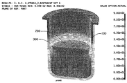
- 1 is a view showing the stress simulation results of the crucible according to the heating of the evaporation source.
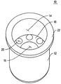
- Figure 2 is a perspective view schematically showing a crucible for metal thin film deposition according to a first embodiment of the present invention.
- Figure 3 is a plan view schematically showing a crucible for depositing a metal thin film according to a first embodiment of the present invention.
- FIG. 4 is a cross-sectional view taken along line AA ′ of FIG. 3.
- FIG. 5 is a cross-sectional view schematically showing an evaporation source for metal thin film deposition having a crucible for metal thin film deposition according to a first embodiment of the present invention.
- FIG. 6 is a state diagram of use of the evaporation source for metal thin film deposition having the crucible for metal thin film deposition according to the first embodiment of the present invention.
- Figure 7 is a plan view schematically showing a crucible for metal thin film deposition according to a second embodiment of the present invention.
- FIG. 8 is a cross-sectional view taken along line BB ′ of FIG. 7.
- FIG. 9 is a plan view schematically showing a crucible for depositing a metal thin film according to a third embodiment of the present invention.
- FIG. 10 is a cross-sectional view taken along the line CC ′ of FIG. 9.
- FIG. 11 is a plan view schematically showing a part of the crucible for depositing a metal thin film according to a fourth embodiment of the present invention.
- FIG. 13 is a schematic cross-sectional view of a crucible for metal thin film deposition according to a fourth embodiment of the present invention.
- first and second may be used to describe various components, but the components should not be limited by the terms. The terms are used only for the purpose of distinguishing one component from another.
- FIG. 1 is a view showing the stress simulation results of the crucible according to the heating of the evaporation source. 1 illustrates a stress state of the crucible 100 when a crucible 100 made of graphite material is filled with aluminum with an evaporation material and heated, and the molten aluminum melts as it is heated. The phase change to the liquid aluminum, it was found that the highest stress 300 is generated at the interface between the free surface 200 and the crucible 100 of the molten aluminum.
- a crucible for depositing a metal thin film which can be prevented from being damaged when the evaporation source is cooled for recharging the evaporation material or maintaining the deposition apparatus while heated to a high temperature for the deposition of metal evaporation material. I would like to present.
- FIG. 2 is a perspective view schematically showing a crucible 10 for depositing a metal thin film according to a first embodiment of the present invention
- FIG. 3 is a schematic view illustrating a crucible 10 for depositing a metal thin film according to a first embodiment of the present invention.
- 4 is a cross-sectional view taken along line AA ′ of FIG. 3.
- 5 is a cross-sectional view schematically showing an evaporation source for depositing a metal thin film having a crucible 10 for depositing a metal thin film according to a first embodiment of the present invention
- FIG. 6 is a view showing a first embodiment of the present invention. It is a state of use of the evaporation source 30 for metal thin film deposition provided with the crucible 10 for metal thin film deposition.
- the crucible 10 the body portion 12, the diffusion portion 14, the first melting hole 16, the stepped portion 18, the second melting hole 20, and the flange 22.
- the metal evaporation material 24, the liquid level 26, the heater portion 28, the evaporation source 30, and the substrate 32 are shown.
- the crucible 10 for depositing a metal thin film is a crucible 10 for depositing a metal thin film to form a metal thin film on the substrate 32 while the metal evaporation material 24 is received and melted and sublimed with heating.
- a top portion of the container shape body portion 12 is opened; And a stepped portion 18 extending inwardly from an inner wall of the body portion 12 so that a first melting hole 16 is formed in a depth direction in the center of the body portion 12.
- a plurality of second melting holes 20 are formed along the stepped portion 18 in a concentric manner around the melting hole 16.
- the evaporation material 24 of the metal is accommodated in the crucible 10 for depositing the metal thin film according to the present embodiment, and the metal evaporation material 24 is sublimed while being heated to form a metal thin film on the substrate 32. Done. At this time, as the metal evaporation material 24, magnesium (Mg), silver (Ag), aluminum (Al) may be applied.
- the body portion 12 has a container shape with an open top.
- a metal evaporation material 24 in a pellet form may be accommodated in the body part 12, and the metal evaporation material 24 is sublimed while the metal evaporation material 24 melts as the heater part is heated around the body part 12. It blows off to the substrate 32 through the open top of the part 12.
- the inside of the body part 12 includes melting holes 16 and 20 through which the metal evaporation material 24 is melted, and a diffusion part 14 communicating with the melting holes 16 and 20 thereon.
- the melting holes 16 and 20 are where the above-mentioned solid metal evaporation material 24 is melted and accommodated, and the metal evaporation material 24 melted in the melting holes 16 and 20 diffuses as the phase changes into gas. It blows off to the board
- the diffusion part 14 is ejected toward the substrate 32 while the evaporation materials 24 phase-changed into gases in the plurality of melting holes 16 and 20 are mixed with each other.
- the stepped portion 18 is formed to extend inward from the inner wall of the body portion 12 so that the first melting hole 16 is formed in the center of the body portion 12 in the depth direction.
- the stepped portion 18 is formed to extend toward the center from the inside of the body portion 12, the stepped portion 18 is formed along the inside of the body portion 12 is formed in the center of the body portion 12
- the first melting hole 16 may be formed.
- the metal evaporation material 24 described above is melted and received in the first melting hole 16.
- the thickness of the crucible 10 forms a step in the depth direction of the crucible 10.
- the plurality of second melting holes 20 are spaced apart from each other in the depth direction in the step portion 18 along the outer circumference of the step portion 18 in the form of concentric circles around the first melting hole 16. Like the first melting hole 16, the metal evaporation material 24 is melted and accommodated in the second melting hole 20.
- the thickness of the crucible 10 is increased in the breaker portion 18 so that heat generated from the heater portion is transferred into the crucible 10. It is difficult to transfer, making it difficult to control the high temperature metal evaporation material 24.
- the stepped portion 18 is formed downward at a position higher than the highest liquid level 26 of the molten metal evaporation material 24.
- the evaporation material 24 of the metal contained in the crucible 10 is melted by heating to phase-change into a liquid evaporation material 24, the free surface and the crucible of the evaporation material 24 in the molten state Since the highest stress is generated at the interface of the (10), in order to prevent the crucible (10) from being damaged, the stepped portion (18) is a crucible at a position higher than the highest level (26) of the molten metal evaporation material (24). 10) is formed downward in the depth direction.
- the liquid level 26 of the evaporation material 24 in the molten state is located at the step 18. Therefore, damage to the crucible 10 is prevented.
- the height of the stepped portion 18 may be determined when the crucible 10 is designed. That is, the height of the stepped portion 18 may be determined by determining the volume of the metal evaporation material 24 accommodated and melting in the crucible 10 and the volume of the melting holes 16 and 20 inside the crucible 10. have.
- the diffusion part 14 which integrates the first melting hole 16 and the second melting hole 20 is formed on the first melting hole 16 and the second melting hole 20.
- the first melting is achieved by setting the formation height of the stepped portion 18 to a position higher than the highest liquid level 26 of the molten metal evaporation material 24 but below a predetermined depth at the upper end of the body portion 12.
- An upper portion of the hole 16 and the second melting hole 20 may be formed with one diffusion part 14 which is integrated while communicating with the first melting hole 16 and the second melting hole 20.
- Evaporating material 24 in a gaseous state sublimed while melting in the first melting hole 16 and the second melting hole 20 flows into the diffusion part 14 and is mixed with each other and ejected in a predetermined distribution from the top of the crucible 10. do.
- the gas state is ejected from each of the first melting hole 16 and the second melting hole 20. Since the distribution of the evaporation material 24 is different from each other, it is difficult to deposit a predetermined thickness on the substrate 32.
- the cross section of the second melting hole 20 may have a circular or rounded arc shape. 3, the second melting hole 20 has a circular cross section.
- the stress due to the phase change of the metal evaporation material 24 may be dispersed without being concentrated in one place.
- stress may be concentrated in accordance with the phase change of the metal evaporation material 24 in the corner portion of the polygon, which may cause damage to the crucible.
- the depth of the second melting hole 20 may be smaller than the depth of the first melting hole 16. Accordingly, the thickness of the bottom of the second melting hole 20 is thicker than the thickness of the bottom of the first melting hole 16.
- the liquid level 26 of the evaporation material 24 in the molten state is gradually lowered.
- the evaporation material 24 in the crucible 10 is almost exhausted and the liquid level 26 of the evaporation material 24 is exhausted.
- the crucible 10 is located at the bottom of the crucible 10
- the second melting hole 20 is located outside of the crucible 10, when the liquid level 26 of the evaporation material 24 is lowered, damage may occur at the bottom thereof.
- the depth of the second melting hole 20 is formed to be smaller than the depth of the first melting hole 16 so as to be formed thicker than the thickness.
- the crucible 10 for depositing a metal thin film may be made of refractory materials, such as graphite, pyrolytic boron nitride (PBN), boron nitride (BN), alumina (Al 2 O 3 ), At least one material selected from aluminum nitride (AlN), molybdenum (Mo), tungsten (W), and tantalum (Ta) may be used.
- refractory materials such as graphite, pyrolytic boron nitride (PBN), boron nitride (BN), alumina (Al 2 O 3 ), At least one material selected from aluminum nitride (AlN), molybdenum (Mo), tungsten (W), and tantalum (Ta) may be used.
- FIG. 5 shows an evaporation source 30 for depositing a metal thin film having a crucible 10 for depositing a metal thin film according to the present embodiment
- FIG. 6 is provided with a crucible 10 for depositing a metal thin film according to the present embodiment.
- a state of use of an evaporation source 30 for depositing a metal thin film is shown.
- the above-described metal thin film deposition crucible 10 is inserted into the metal thin film deposition evaporation source 30 for heating it, and as the heater unit 28 heats the crucible 10, the metal evaporation inside the crucible 10.
- the material 24 is melted and sublimed to perform deposition on the substrate 32.
- the heater 28 is disposed on the outer circumference of the crucible 10 to heat the crucible 10 so that the metal evaporation material 24 is melted and sublimed.
- the outer circumference of the heater unit 28 may be provided with a reflector (not shown) for reflecting the heat generated from the heater unit 28 back toward the crucible 10.
- the heater unit 28 may be manufactured in a cylindrical shape in which a heating wire is disposed therein, and a flange 22 is formed at an upper end of the crucible 10 for depositing a metal thin film, so that the crucible 10 is disposed in the heater unit 28.
- the flange 22 may be configured to be supported by the heater unit 28 while being inserted.
- the evaporation source 30 for depositing the metal thin film having the crucible 10 for depositing the metal thin film according to the present embodiment is, as shown in FIG. 6, the substrate 32 in a vacuum chamber (not shown) in a vacuum state. Are arranged opposite.
- the solid metal evaporation material 24 is melted in accordance with the heating of the crucible 10 and is phase-changed into the liquid metal evaporation material 24, and then the substrate is ejected from the crucible 10 while being sublimated into a gas and disposed to face each other. Is deposited on 32.
- FIG. 7 is a plan view schematically illustrating a crucible 10 for depositing a metal thin film according to a second embodiment of the present invention
- FIG. 8 is a cross-sectional view taken along line BB ′ of FIG. 7.
- the crucible 10 the body portion 12, the diffusion portion 14, the first melting hole 16, the stepped portion 18, the second melting hole 20 ′, and the flange 22.
- Metal evaporation material 24 and liquid level 26 are shown.
- a cross section of each second melting hole 20 ′ formed concentrically on the outer circumference of the first melting hole 16 is formed in an arc shape having a rounded corner.
- the plurality of second melting holes 20 ′ form a circular shape as a whole.
- the cross section of the second melting hole 20 ′ is formed in an arc shape having rounded corners, so that the stress due to the phase change of the evaporation material 24 of the metal may be dispersed without being concentrated in one place.
- the height of the step portion 18 is formed downward at a position higher than the highest liquid level 26 of the metal evaporation material 24 to be melted, and the second melting hole 20 ') Is formed smaller than the depth of the first melting hole (16).
- Other components are the same as those of the first embodiment described above, and thus description thereof will be omitted.
- FIG. 9 is a plan view schematically illustrating a crucible 10 for depositing a metal thin film according to a third exemplary embodiment of the present invention
- FIG. 10 is a cross-sectional view taken along the line CC ′ of FIG. 9.
- the crucible 10 the body portion 12, the diffusion portion 14, the first melting hole 16, the stepped portion 18, the second melting hole 20 ′′ and the flange ( 22, metal evaporation material 24, liquid level 26 is shown.
- the crucible 10 for depositing the metal thin film according to the present embodiment has a shape in which two concentric second melting holes 20 ′ and 20 ′′ are formed around the first melting hole 16. As the second melt holes 20 'and 20' 'are formed in multiple, the cross-sectional size of the first melt holes 16 is reduced, and concentric second melt holes 20' and 20 '' are formed around the second melt holes 20 'and 20' '. Concentric form of multiple forms. In the present embodiment, the depth of the outermost second melting hole 20 ′ may be smaller than the depth of the inner second melting hole 20 ′′ for the same reason as described above.
- FIG. 11 is a schematic cross-sectional view of a crucible 10 for depositing a metal thin film according to a fourth embodiment of the present invention.
- 12 is a plan view schematically illustrating a body 12 of the crucible 10 for depositing a metal thin film according to a fourth embodiment of the present invention
- FIG. 13 is a cross-sectional view taken along the line D-D 'of FIG. 12. to be.
- the crucible 10 the body part 12, the diffusion part 14, the first melting hole 16, the stepped part 18, the second melting hole 20, and the metal evaporation material 24 are illustrated.
- the liquid level 26, the inner housing 34, and the outer housing 36 are shown.
- the crucible 10 for depositing a metal thin film according to the present embodiment is configured in multiple forms to enhance the strength of the crucible 10.
- the crucible 10 for depositing a metal thin film according to the present embodiment has a shape in which an inner housing 34 and an outer housing 36 are disposed on an outer side of the body portion 12 of the above-described type. That is, the crucible 10 according to the present embodiment has an inner housing 34 in which the body portion 12 is embedded so that the outer surface of the body portion 12 is in contact with the inner surface, and an outer surface of the inner housing 34 on the inner surface. It includes an outer housing 36 in which the inner housing 34 is built in contact.
- the crucible 10 is composed of a body portion 12, an inner housing 34, and an outer housing 36 to improve the strength of the crucible 10 to prevent breakage of the crucible 10.
- the inner housing 34 and the outer housing 36 may be made of refractory.
- the inner housing 34 is formed of a material including aluminum nitride (AIN), and the outer housing 36 is formed. It was formed of a material containing pyrolytic boron nitride (PBN: Pyrolytic Boron Nitride). Pyrolysis boron nitride is a refractory material so that the heat heated in the heater unit 28 is evenly distributed into the crucible 10 through the outer housing 36 due to the properties of the material, and aluminum nitride is a material having excellent heat resistance and high thermal conductivity. It serves to directly transfer the heat transferred from the outer housing 36 made of boron nitride to the inner body portion 12.
- PBN Pyrolytic Boron Nitride
- the inner body portion 12 may be formed as shown in the first to third embodiments above. However, referring to FIG. 13, when the bottom of the body portion 12 is formed to have a thick thickness to prevent breakage at the bottom, the depths of the first melting hole 16 and the second melting hole 20 are the same. Can be formed.
Landscapes
- Physical Vapour Deposition (AREA)
Abstract
La présente invention concerne, dans un aspect, un creuset pour dépôt de film mince métallique, dans lequel un matériau vaporisé d'un métal est contenu et fondu puis sublimé par chauffage pour former un film mince métallique sur un substrat, le creuset comportant: une partie de corps en forme de récipient présentant une extrémité supérieure ouverte; et une partie étagée s'étendant vers l'intérieur à partir d'une paroi intérieure de la partie de corps de façon à former un premier trou de fusion dans le sens d'une profondeur au centre de la partie de corps, une pluralité de deuxièmes trous de fusion étant formée de façon concentrique le long de la partie étagée autour du premier trou de fusion.
Priority Applications (1)
| Application Number | Priority Date | Filing Date | Title |
|---|---|---|---|
| CN201580085778.XA CN108713262B (zh) | 2015-12-18 | 2015-12-21 | 用于金属薄膜沉积的坩埚及用于金属薄膜沉积的蒸发源 |
Applications Claiming Priority (2)
| Application Number | Priority Date | Filing Date | Title |
|---|---|---|---|
| KR1020150181752A KR101761700B1 (ko) | 2015-12-18 | 2015-12-18 | 금속 박막 증착용 도가니 및 금속 박막 증착용 증발원 |
| KR10-2015-0181752 | 2015-12-18 |
Publications (1)
| Publication Number | Publication Date |
|---|---|
| WO2017104885A1 true WO2017104885A1 (fr) | 2017-06-22 |
Family
ID=59056908
Family Applications (1)
| Application Number | Title | Priority Date | Filing Date |
|---|---|---|---|
| PCT/KR2015/014031 Ceased WO2017104885A1 (fr) | 2015-12-18 | 2015-12-21 | Creuset pour dépôt de film mince métallique et source d'évaporation pour dépôt de film mince métallique |
Country Status (3)
| Country | Link |
|---|---|
| KR (1) | KR101761700B1 (fr) |
| CN (1) | CN108713262B (fr) |
| WO (1) | WO2017104885A1 (fr) |
Cited By (1)
| Publication number | Priority date | Publication date | Assignee | Title |
|---|---|---|---|---|
| US20190055642A1 (en) * | 2017-08-17 | 2019-02-21 | Wuhan China Star Optoelectronics Semiconductor Dis play Technology Co., Ltd. | Vapor evaporation source |
Families Citing this family (3)
| Publication number | Priority date | Publication date | Assignee | Title |
|---|---|---|---|---|
| CN209619438U (zh) * | 2019-01-17 | 2019-11-12 | 云谷(固安)科技有限公司 | 一种点蒸发源以及蒸镀设备 |
| KR20200134531A (ko) | 2019-05-22 | 2020-12-02 | 주식회사 선익시스템 | 열차단부를 구비한 도가니부재 |
| WO2021107223A1 (fr) * | 2019-11-29 | 2021-06-03 | 엘지전자 주식회사 | Creuset pour dépôt |
Citations (5)
| Publication number | Priority date | Publication date | Assignee | Title |
|---|---|---|---|---|
| JPH0733305B2 (ja) * | 1987-03-20 | 1995-04-12 | 三菱マテリアル株式会社 | 石英製二重ルツボの製造方法 |
| KR20080013686A (ko) * | 2006-08-08 | 2008-02-13 | 순천향대학교 산학협력단 | 대면적 기판에 박막을 적층하기 위한 장치 |
| KR20130073406A (ko) * | 2011-12-23 | 2013-07-03 | 주식회사 원익아이피에스 | 방열조립체를 포함하는 고온 증발원 |
| KR20130073407A (ko) * | 2011-12-23 | 2013-07-03 | 주식회사 원익아이피에스 | 외부 가열용기를 포함하는 고온 증발원 |
| KR20140042656A (ko) * | 2012-09-28 | 2014-04-07 | 가부시키가이샤 히다치 하이테크놀로지즈 | 증발원, 진공 증착 장치 및 유기 el 표시 장치 제조 방법 |
Family Cites Families (1)
| Publication number | Priority date | Publication date | Assignee | Title |
|---|---|---|---|---|
| KR20110095982A (ko) * | 2010-02-20 | 2011-08-26 | 진중 김 | 씨아이지에스 박막제조용 병합증발원 |
-
2015
- 2015-12-18 KR KR1020150181752A patent/KR101761700B1/ko active Active
- 2015-12-21 WO PCT/KR2015/014031 patent/WO2017104885A1/fr not_active Ceased
- 2015-12-21 CN CN201580085778.XA patent/CN108713262B/zh active Active
Patent Citations (5)
| Publication number | Priority date | Publication date | Assignee | Title |
|---|---|---|---|---|
| JPH0733305B2 (ja) * | 1987-03-20 | 1995-04-12 | 三菱マテリアル株式会社 | 石英製二重ルツボの製造方法 |
| KR20080013686A (ko) * | 2006-08-08 | 2008-02-13 | 순천향대학교 산학협력단 | 대면적 기판에 박막을 적층하기 위한 장치 |
| KR20130073406A (ko) * | 2011-12-23 | 2013-07-03 | 주식회사 원익아이피에스 | 방열조립체를 포함하는 고온 증발원 |
| KR20130073407A (ko) * | 2011-12-23 | 2013-07-03 | 주식회사 원익아이피에스 | 외부 가열용기를 포함하는 고온 증발원 |
| KR20140042656A (ko) * | 2012-09-28 | 2014-04-07 | 가부시키가이샤 히다치 하이테크놀로지즈 | 증발원, 진공 증착 장치 및 유기 el 표시 장치 제조 방법 |
Cited By (2)
| Publication number | Priority date | Publication date | Assignee | Title |
|---|---|---|---|---|
| US20190055642A1 (en) * | 2017-08-17 | 2019-02-21 | Wuhan China Star Optoelectronics Semiconductor Dis play Technology Co., Ltd. | Vapor evaporation source |
| US10801101B2 (en) * | 2017-08-17 | 2020-10-13 | Wuhan China Star Optoelectronics Semiconductor Display Technology Co., Ltd. | Vapor evaporation source |
Also Published As
| Publication number | Publication date |
|---|---|
| KR20170073171A (ko) | 2017-06-28 |
| CN108713262B (zh) | 2021-02-26 |
| CN108713262A (zh) | 2018-10-26 |
| KR101761700B1 (ko) | 2017-07-28 |
Similar Documents
| Publication | Publication Date | Title |
|---|---|---|
| CN1679375B (zh) | 制造系统,发光装置以及含有有机化合物层的制造方法 | |
| KR100826743B1 (ko) | 유기 박막의 제조장치 | |
| WO2017104885A1 (fr) | Creuset pour dépôt de film mince métallique et source d'évaporation pour dépôt de film mince métallique | |
| CN101960041B (zh) | 成膜源、蒸镀装置、有机el元件的制造装置 | |
| JP2009087931A (ja) | 成膜方法、蒸着装置、有機el製造装置 | |
| US20140056579A1 (en) | Electrode cover and evaporation device | |
| JP2019031705A (ja) | 蒸発源装置およびその制御方法 | |
| CN1950537A (zh) | 蒸发装置、蒸镀装置以及蒸镀装置中的蒸发装置的切换方法 | |
| CN1769514B (zh) | 加热熔罐和包括该加热熔罐的沉积装置 | |
| KR101202229B1 (ko) | 증기 발생 장치, 증착 장치 | |
| KR20040068000A (ko) | 백색광 방출 유기발광다이오드의 제조에서 치밀화된 유기물질의 사용 | |
| JP5798452B2 (ja) | 蒸発源 | |
| JP3817054B2 (ja) | 蒸着源用るつぼ、及び蒸着装置 | |
| KR100858914B1 (ko) | 박막 증착 장치 | |
| WO2011155661A1 (fr) | Cellule d'effusion linéaire, son procédé de fabrication et évaporateur l'utilisant | |
| JP2007314877A (ja) | 電極カバーおよび蒸着装置 | |
| WO2021085685A1 (fr) | Agencement de dépôt de matériau, système de dépôt sous vide et procédé de fabrication d'un agencement de dépôt de matériau | |
| WO2020004853A1 (fr) | Source de dépôt sous vide, procédé de préparation d'affichage électroluminescent organique l'utilisant et affichage électroluminescent organique | |
| KR101436898B1 (ko) | 증발 소스 및 그를 구비하는 평판표시소자의 증발 장치 | |
| KR200365703Y1 (ko) | 유기 박막 증착 장치 | |
| CN106337165A (zh) | 沉积源、沉积装置及利用沉积装置的显示装置制造方法 | |
| WO2012153887A1 (fr) | Appareil destiné à apporter des matières premières | |
| WO2019031647A1 (fr) | Procédé de formation de couche de film mince organique oled a l'aide d'un dispositif de pulvérisation rf, dispositif de pulvérisation rf et dispositif de formation de cible utilisée dans un dispositif de pulvérisation rf | |
| JP2003222472A (ja) | ルツボ | |
| KR100583044B1 (ko) | 선형 증착물질 가열장치 |
Legal Events
| Date | Code | Title | Description |
|---|---|---|---|
| 121 | Ep: the epo has been informed by wipo that ep was designated in this application |
Ref document number: 15910806 Country of ref document: EP Kind code of ref document: A1 |
|
| NENP | Non-entry into the national phase |
Ref country code: DE |
|
| 122 | Ep: pct application non-entry in european phase |
Ref document number: 15910806 Country of ref document: EP Kind code of ref document: A1 |