WO2017107045A1 - Procédé de réparation et puce de réparation pour cartouche d'encre remise à neuf, et cartouche d'encre remise à neuf - Google Patents
Procédé de réparation et puce de réparation pour cartouche d'encre remise à neuf, et cartouche d'encre remise à neuf Download PDFInfo
- Publication number
- WO2017107045A1 WO2017107045A1 PCT/CN2015/098212 CN2015098212W WO2017107045A1 WO 2017107045 A1 WO2017107045 A1 WO 2017107045A1 CN 2015098212 W CN2015098212 W CN 2015098212W WO 2017107045 A1 WO2017107045 A1 WO 2017107045A1
- Authority
- WO
- WIPO (PCT)
- Prior art keywords
- printer
- data
- repair
- command
- address
- Prior art date
- Legal status (The legal status is an assumption and is not a legal conclusion. Google has not performed a legal analysis and makes no representation as to the accuracy of the status listed.)
- Ceased
Links
Images

Classifications
-
- G—PHYSICS
- G03—PHOTOGRAPHY; CINEMATOGRAPHY; ANALOGOUS TECHNIQUES USING WAVES OTHER THAN OPTICAL WAVES; ELECTROGRAPHY; HOLOGRAPHY
- G03G—ELECTROGRAPHY; ELECTROPHOTOGRAPHY; MAGNETOGRAPHY
- G03G15/00—Apparatus for electrographic processes using a charge pattern
- G03G15/55—Self-diagnostics; Malfunction or lifetime display
- G03G15/553—Monitoring or warning means for exhaustion or lifetime end of consumables, e.g. indication of insufficient copy sheet quantity for a job
-
- B—PERFORMING OPERATIONS; TRANSPORTING
- B41—PRINTING; LINING MACHINES; TYPEWRITERS; STAMPS
- B41J—TYPEWRITERS; SELECTIVE PRINTING MECHANISMS, i.e. MECHANISMS PRINTING OTHERWISE THAN FROM A FORME; CORRECTION OF TYPOGRAPHICAL ERRORS
- B41J2/00—Typewriters or selective printing mechanisms characterised by the printing or marking process for which they are designed
- B41J2/005—Typewriters or selective printing mechanisms characterised by the printing or marking process for which they are designed characterised by bringing liquid or particles selectively into contact with a printing material
- B41J2/01—Ink jet
- B41J2/17—Ink jet characterised by ink handling
- B41J2/175—Ink supply systems ; Circuit parts therefor
- B41J2/17503—Ink cartridges
- B41J2/17543—Cartridge presence detection or type identification
- B41J2/17546—Cartridge presence detection or type identification electronically
-
- B—PERFORMING OPERATIONS; TRANSPORTING
- B41—PRINTING; LINING MACHINES; TYPEWRITERS; STAMPS
- B41J—TYPEWRITERS; SELECTIVE PRINTING MECHANISMS, i.e. MECHANISMS PRINTING OTHERWISE THAN FROM A FORME; CORRECTION OF TYPOGRAPHICAL ERRORS
- B41J2/00—Typewriters or selective printing mechanisms characterised by the printing or marking process for which they are designed
- B41J2/005—Typewriters or selective printing mechanisms characterised by the printing or marking process for which they are designed characterised by bringing liquid or particles selectively into contact with a printing material
- B41J2/01—Ink jet
- B41J2/17—Ink jet characterised by ink handling
- B41J2/175—Ink supply systems ; Circuit parts therefor
- B41J2/17503—Ink cartridges
-
- B—PERFORMING OPERATIONS; TRANSPORTING
- B41—PRINTING; LINING MACHINES; TYPEWRITERS; STAMPS
- B41J—TYPEWRITERS; SELECTIVE PRINTING MECHANISMS, i.e. MECHANISMS PRINTING OTHERWISE THAN FROM A FORME; CORRECTION OF TYPOGRAPHICAL ERRORS
- B41J2/00—Typewriters or selective printing mechanisms characterised by the printing or marking process for which they are designed
- B41J2/005—Typewriters or selective printing mechanisms characterised by the printing or marking process for which they are designed characterised by bringing liquid or particles selectively into contact with a printing material
- B41J2/01—Ink jet
- B41J2/17—Ink jet characterised by ink handling
- B41J2/175—Ink supply systems ; Circuit parts therefor
- B41J2/17503—Ink cartridges
- B41J2/17559—Cartridge manufacturing
-
- G—PHYSICS
- G03—PHOTOGRAPHY; CINEMATOGRAPHY; ANALOGOUS TECHNIQUES USING WAVES OTHER THAN OPTICAL WAVES; ELECTROGRAPHY; HOLOGRAPHY
- G03G—ELECTROGRAPHY; ELECTROPHOTOGRAPHY; MAGNETOGRAPHY
- G03G21/00—Arrangements not provided for by groups G03G13/00 - G03G19/00, e.g. cleaning, elimination of residual charge
- G03G21/16—Mechanical means for facilitating the maintenance of the apparatus, e.g. modular arrangements
- G03G21/18—Mechanical means for facilitating the maintenance of the apparatus, e.g. modular arrangements using a processing cartridge, whereby the process cartridge comprises at least two image processing means in a single unit
- G03G21/1875—Mechanical means for facilitating the maintenance of the apparatus, e.g. modular arrangements using a processing cartridge, whereby the process cartridge comprises at least two image processing means in a single unit provided with identifying means or means for storing process- or use parameters, e.g. lifetime of the cartridge
-
- G—PHYSICS
- G03—PHOTOGRAPHY; CINEMATOGRAPHY; ANALOGOUS TECHNIQUES USING WAVES OTHER THAN OPTICAL WAVES; ELECTROGRAPHY; HOLOGRAPHY
- G03G—ELECTROGRAPHY; ELECTROPHOTOGRAPHY; MAGNETOGRAPHY
- G03G21/00—Arrangements not provided for by groups G03G13/00 - G03G19/00, e.g. cleaning, elimination of residual charge
- G03G21/16—Mechanical means for facilitating the maintenance of the apparatus, e.g. modular arrangements
- G03G21/18—Mechanical means for facilitating the maintenance of the apparatus, e.g. modular arrangements using a processing cartridge, whereby the process cartridge comprises at least two image processing means in a single unit
- G03G21/1875—Mechanical means for facilitating the maintenance of the apparatus, e.g. modular arrangements using a processing cartridge, whereby the process cartridge comprises at least two image processing means in a single unit provided with identifying means or means for storing process- or use parameters, e.g. lifetime of the cartridge
- G03G21/1878—Electronically readable memory
-
- G—PHYSICS
- G03—PHOTOGRAPHY; CINEMATOGRAPHY; ANALOGOUS TECHNIQUES USING WAVES OTHER THAN OPTICAL WAVES; ELECTROGRAPHY; HOLOGRAPHY
- G03G—ELECTROGRAPHY; ELECTROPHOTOGRAPHY; MAGNETOGRAPHY
- G03G21/00—Arrangements not provided for by groups G03G13/00 - G03G19/00, e.g. cleaning, elimination of residual charge
- G03G21/16—Mechanical means for facilitating the maintenance of the apparatus, e.g. modular arrangements
- G03G21/18—Mechanical means for facilitating the maintenance of the apparatus, e.g. modular arrangements using a processing cartridge, whereby the process cartridge comprises at least two image processing means in a single unit
- G03G21/1875—Mechanical means for facilitating the maintenance of the apparatus, e.g. modular arrangements using a processing cartridge, whereby the process cartridge comprises at least two image processing means in a single unit provided with identifying means or means for storing process- or use parameters, e.g. lifetime of the cartridge
- G03G21/1878—Electronically readable memory
- G03G21/1882—Electronically readable memory details of the communication with memory, e.g. wireless communication, protocols
-
- G—PHYSICS
- G06—COMPUTING OR CALCULATING; COUNTING
- G06F—ELECTRIC DIGITAL DATA PROCESSING
- G06F13/00—Interconnection of, or transfer of information or other signals between, memories, input/output devices or central processing units
-
- G—PHYSICS
- G03—PHOTOGRAPHY; CINEMATOGRAPHY; ANALOGOUS TECHNIQUES USING WAVES OTHER THAN OPTICAL WAVES; ELECTROGRAPHY; HOLOGRAPHY
- G03G—ELECTROGRAPHY; ELECTROPHOTOGRAPHY; MAGNETOGRAPHY
- G03G15/00—Apparatus for electrographic processes using a charge pattern
- G03G15/06—Apparatus for electrographic processes using a charge pattern for developing
- G03G15/08—Apparatus for electrographic processes using a charge pattern for developing using a solid developer, e.g. powder developer
- G03G15/0894—Reconditioning of the developer unit, i.e. reusing or recycling parts of the unit, e.g. resealing of the unit before refilling with toner
-
- G—PHYSICS
- G03—PHOTOGRAPHY; CINEMATOGRAPHY; ANALOGOUS TECHNIQUES USING WAVES OTHER THAN OPTICAL WAVES; ELECTROGRAPHY; HOLOGRAPHY
- G03G—ELECTROGRAPHY; ELECTROPHOTOGRAPHY; MAGNETOGRAPHY
- G03G2215/00—Apparatus for electrophotographic processes
- G03G2215/00987—Remanufacturing, i.e. reusing or recycling parts of the image forming apparatus
Definitions
- the invention relates to the field of printing and imaging, and in particular to a method for repairing a remanufactured ink cartridge, a repairing chip and a remanufactured ink cartridge.
- Existing printer cartridge chips include enable contacts, data contacts, address contacts, and clock contacts that communicate with the printer's enable, data, address, and clock lines, receive commands from the printer, and respond
- the cartridge cartridge stores the relevant usage and configuration information of the cartridge.
- the original ink cartridge manufacturer uses a method that cannot directly reset the ink cartridge usage information, for example, the storage unit uses a fuse bit to record the ink amount information.
- the storage unit on the ink cartridge records the status information that the ink has been exhausted, making the ink cartridge unusable.
- a cartridge manufacturer developed a repair chip to reset the outside of the chip and the original chip of the ink cartridge, so that when the printer obtains the ink remaining information of the ink cartridge, the feedback information of the ink cartridge reflects the information that the ink cartridge is not exhausted.
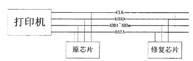
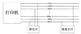
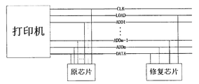
- Existing repair chips typically have the same number of enable contacts, data contacts, address contacts, and clock contacts as the original cartridge of the cartridge. As shown in FIG. 1, the repair chip is electrically connected to the corresponding contacts of the original chip, and is electrically connected to the enable line, the data line, the address line, and the clock line of the printer.
- the repair chip receives the command information from the printer according to the communication protocol between the printer and the original chip of the ink cartridge, and when the printer sends the read data command, the return data of the original chip is modified, so that the printer considers that the ink of the ink cartridge is not exhausted, so that the ink cartridge can Continue to get used.
- all the contacts of the original chip need to be electrically connected with the repair chip, and since the original chip and the repair chip are small in size, the contact area is small, and the solder joint and the solder joint are prone to occur during the soldering process. , short circuit and other issues.
- the individual contacts of the original chip and the repair chip need to be inspected one by one to ensure that they are electrically connected well after the welding is completed. Therefore, the more contacts that need to be connected between the original chip and the repair chip, the more contacts that need to be soldered on the same tiny circuit board, which increases the difficulty of soldering; the connection between the original chip and the repair chip needs to be connected. The more contacts, the greater the difficulty of soldering, the more ink cartridges are scrapped due to poor soldering; the more contacts that need to be connected between the original chip and the repair chip, the more contacts that need to be inspected later, the more ink cartridges are added. Recycling workload.
- the repair chip comprises: a substrate, a substrate having a front side and a back side; a hollow portion disposed at a position substantially and the hollow portion corresponds to the flexible circuit board of the ink cartridge (ie, the original chip of the ink cartridge) the position of the nozzle control contact; the memory unit contact is disposed on the front side of the substrate and the memory unit contact is electrically connected to the memory unit of the repair chip; the signal can pass through the contact and is disposed on the substrate
- the opposite sides, and the signals corresponding to the positions on the front and back sides can communicate with each other through the contacts.
- the utility model repair chip is mounted to When the ink cartridge is on the flexible circuit board, the position of the repair chip can be ensured to be accurate, and the risk of short circuit caused when the repair chip is electrically connected to the flexible circuit board of the ink cartridge is reduced to some extent, and the yield of the remanufactured ink cartridge is improved. However, in the case where the number of contacts to be soldered is still large, a relatively large portion of the product will still be scrapped due to a short circuit.
- the invention provides a repairing method for a remanufactured ink cartridge according to the prior art, which is caused by excessive electric shock that needs to be soldered during the repair process of the remanufactured ink cartridge, and is suitable for the repair chip storing the repair data, characterized in that the repairing The chip returns all or part of the repair data to the printer via the data line of the printer based on the 0 to n-1 auxiliary lines of the printer and the signal on the printer's enable line.
- the auxiliary line includes an address line and a clock line of the printer; repair data: data for making the information indicating the remaining ink amount of the ink cartridge of the ink cartridge not 0; n: equal to the sum of the address line of the printer and the number of the clock lines.
- the repair chip does not need to monitor all the lines of the printer, and only needs to monitor the printer's enable line, data line, and 0 to n-1 auxiliary lines. Thereby, the number of contacts electrically connected to the printer and the original chip is reduced, thereby simplifying the welding difficulty and the workload in the process of regenerating the ink cartridge, and reducing the risk of scrapping the ink cartridge during the repair process from the source.
- the repair chip judges the type of command sent by the printer according to the characteristics of the communication protocol between the original chip of the ink cartridge and the printer, and judges that the command sent by the printer is valid according to the signal characteristics of the monitored and a small number of printer lines. When reading a data command, the data that the printer needs to acquire is determined based only on the signals on the monitored, smaller number of printer lines, and is returned to the printer through the printer's data line.
- the repair chip determines whether the command sent by the printer is a valid read data command according to the printer's 1 to m-1 address line and the signal on the enable line; and the command sent by the printer is a valid read data command. All or part of the repair data is returned to the printer through the data line of the printer. Where m: is equal to the number of address lines of the printer.
- a valid enable signal appears on the enable line of the printer: if at most one of the 1 to m-1 address lines of the printer has a signal, it is determined that the command sent by the printer is a valid read data. Command; otherwise, it is determined that the printer sends a command that is not a valid read data command.
- the repair chip determines the printer according to the time interval between the valid enable signal on the printer's enable line and the time interval between the printer's clock signal or the valid enable signal appearing on the printer's enable line. Whether the sent command is a valid read data command; and returns all or part of the repair fix to the printer through the printer's data line when the command sent by the printer is a valid read data command.
- the method for determining whether the printer sends a command as a valid read data command is: comparing the time interval with a preset time interval minimum value and a preset time interval maximum value: if the time interval is greater than a preset time Interval If the maximum value or the time interval is less than the preset minimum time interval, it is determined that the printer sends a command that is not a valid read data command; if the time interval is greater than or equal to a preset time interval minimum value and less than or equal to a preset time The interval maximum value determines whether the printer sends a command as a valid read data command.
- the valid enable signal when a valid enable signal appears on the enable line of the printer, it is determined whether the valid enable signal is the first valid enable signal. For the first valid enable signal, return all or part of the repair data to the printer through the printer's data line; for non-first valid enable signal: when determining whether the printer command is a valid read data command, pass all or part of the repair data through the printer The data line is returned to the printer.
- the repair chip determines whether the valid enable signal appearing on the enable line of the printer is the first valid enable signal according to the first enable signal flag.
- the value of the first enable signal flag is set to a value indicating that the valid enable signal appearing on the enable line of the printer is a non-first effective enable signal after a valid enable occurs on the enable line of the printer.
- the command sent by the printer is valid read data according to the time interval between the valid enable signals appearing on the enable line.
- the valid enable signal appears on the enable line of the printer, if the first enable signal flag is true, the valid enable signal is determined to be the first valid enable signal, otherwise it is determined that the valid enable signal is not enabled for the first time. signal.
- the first valid enable signal return all or part of the repair data to the printer through the printer's data line, and set the first valid enable signal to false.
- For non-first effective enable signal when determining whether the printer command is a valid read data command, return all or part of the repair data to the printer through the data line of the printer; when determining that the printer command is not a valid read data command, Set the first valid enable signal to true and set the data index value to the initial value.
- the data index value the data index value corresponds to the address of the repair data that needs to be returned in the repair chip; the first enable signal flag: mark whether the received valid enable signal is the first valid enable signal. symbols of.
- the repair chip determines the data that the printer needs to acquire:
- the repair chip determines the repair data that needs to be returned to the printer based on the m-1 address line of the printer and the signal on the printer's enable line: when a valid enable signal appears on the enable line of the printer
- the signal on the m-1 address line of the printer determines the address block where the repaired data needs to be returned.
- the repair data that needs to be returned is found in the address block according to the data index value, and the repair data that needs to be returned is returned to the printer through the data line of the printer.
- Comparing the data index value with a data index maximum value of the address block if the data index value is smaller than a data index maximum value of the address block, adding the data index value to 1; if greater than or equal to the address The data index maximum of the block, which is set to the initial value.
- the data index value the data index value is in one-to-one correspondence with the address of the repair data in the address block in the address block; m: equal to the number of address lines of the printer.
- the signal on the m-1 address line of the printer determines that the address block in which the repair data needs to be returned is: according to the address block stored in the repair chip. With printer One-to-one correspondence of address lines.
- a valid enable signal appears on the enable line of the printer: If the m-1 address line of the printer has no signal, the address block where the repair data needs to be returned is the address line that the repair chip does not monitor. The address block; if there is one and only one address line in the m-1 root address line of the printer, the address block where the repaired data needs to be returned is the address block corresponding to the address line with the signal.
- the repair chip returns all or part of the repair data to the printer through the data line of the printer in a predetermined order.
- the present invention also provides a repair chip for a remanufactured ink cartridge, comprising a storage device for storing repair data, wherein the repair chip comprises: 0 to n for monitoring 0 to n-1 auxiliary line electrical connections of the printer - 1 auxiliary contact; an enable contact for monitoring the enable connection of the printer; 0 to n -1 auxiliary lines of the printer monitored according to the address contact and the enable contact
- the signal returns all or part of the repair data to the data return device of the printer through the data contact.
- the auxiliary line includes the address line and the clock line of the printer;
- the auxiliary contact includes an address contact for monitoring the address line of the printer and a clock contact for monitoring the clock line of the printer;
- repair data used to make the ink cartridge represent the remaining ink cartridge
- the information of the ink amount is not 0 data;
- n is equal to the sum of the address line of the printer and the number of clock lines.
- the repair chip includes command determining means for determining whether the command sent by the printer is a valid read data command based on the printer signals monitored by the 1 to m-1 address contacts and the enable contacts; the data return The device determines, according to the judgment result of the command, when the command sent by the printer is a valid read data command, returns all or part of the repair data to the printer through the data contact.
- m is equal to the number of address lines of the printer.
- the repair chip comprises: a timer, calculating a time interval between a valid enable signal of the printer detected by the enable contact and a clock signal of the printer monitored by the clock contact, or calculating The time interval between the printer enable enable signals monitored by the enable contacts; the command determining means determining whether the command sent by the printer is a valid read data command according to the time interval.
- the data transmitting device returns all or part of the repair repair to the printer through the data contact when determining that the command sent by the printer is a valid read data command according to the judgment result of the command determining device.
- the command judging means includes a command judging unit.
- the command judging unit judges that the command sent by the printer is a valid read data command when at most one address contact of the 1 to m-1 address contacts monitors the signal; otherwise, it is determined that the printer sends the command is not valid. Read data command.
- the command judging device comprises: a comparator, comparing the time interval with a preset time interval minimum value, and the time interval and a preset time interval maximum value.
- the command determining device determines that the printer sends a life when the time interval is greater than a preset time interval maximum value or the time interval is less than a preset time interval minimum value.
- the read data command is not valid; when the time interval is greater than or equal to a preset minimum time interval and less than or equal to a preset time interval maximum value, it is determined that the printer sends the command as a valid read data command.
- the repair chip further includes: a first effective enable signal judging device, and when the enable contact monitors a valid enable signal on the enable line of the printer, determining whether the valid enable signal is valid for the first time Enable signal.
- the data returning device returns all or part of the repair data to the printer through the data contact when the enable contact detects the first valid enable signal according to the determination result of the first valid enable signal determining device.
- the command judging device judges whether the printer command is a valid read data command when the enable contact detects a non-first valid enable signal according to the judgment result of the first valid enable signal judging device.
- the data returning device returns all or part of the repair data to the said data contact through the data contact when the command determining means determines that the command sent by the printer is a valid read data command according to the judgment result of the command determining means printer.
- the storage device stores the first enable signal flag and the data index value, and when the command determining device determines that the printer command is not a valid read data command, sets the first valid enable signal to be true, and sets the data index value.
- the data index value the data index value corresponds to the address of the repair data that needs to be returned in the repair chip; the first enable signal flag: mark whether the received valid enable signal is the first valid enable signal. symbols of.
- said storage means stores a first enable signal flag for indicating whether said valid enable signal monitored by said enable contact is a first valid enable signal; said first enable signal flag value is The enable contact monitors that the valid enable signal is later set to indicate that the effective enable signal monitored by the enable contact is a value other than the first active enable signal.
- the data returning device comprises: an address determining means, determining, according to the signals monitored by the m-1 address contacts, an address block in which the repair data to be returned is located; and the data transmitting means in the address block according to
- the data index value finds the repair data that needs to be returned, and returns the repair data that needs to be returned to the printer through the data line of the printer; the comparator compares the data index value with the data index maximum value of the address block; a counter, if the data index value is smaller than a data index maximum value of the address block, adding 1 to the data index value; if the data index value is greater than or equal to a data index maximum value of the address block, The data index value is set to the initial value.
- the data index value is in one-to-one correspondence with the address of the repair data in the address block in the address block; m: equal to the number of address lines of the printer.
- said address determining means comprises: an address block memory for storing a one-to-one correspondence of said memory printer address lines and address blocks. If the address contact does not detect a signal on the m-1 address line of the printer, the address determining means determines that the address block in which the repair data needs to be returned is: the address block memory and the repair chip are not The address block corresponding to the monitored address line; if the address contact detects the m-1 of the printer One of the address lines has a signal, and the address determining means determines that the address block in which the repair data needs to be returned is in the address block corresponding to the address line having the signal in the address block memory.
- said data return means returns all or part of the repair data to the printer via the data line of the printer in a predetermined sequence.
- the invention also provides a remanufactured ink cartridge, comprising an ink cartridge body and a original chip mounted on the ink cartridge body, wherein the remanufactured ink cartridge further comprises the aforementioned repair chip, the enable contact of the repair chip and The enable contacts of the original chip are electrically connected, and the data contacts of the repair chip are electrically connected to the data contacts of the original chip.
- the address contact of the repair chip is electrically coupled to the address contact of the original chip.
- the clock contact of the repair chip is electrically coupled to the clock contact of the original chip.
- the ink cartridge scraping rate is reduced during the production process of the ink cartridge, which improves the utilization rate of the waste ink cartridge, reduces the waste of the ink cartridge, and is more energy-saving and environmentally friendly.
- FIG. 1 is a schematic diagram of electrical connections between a repair chip and a original chip and a printer in the prior art.
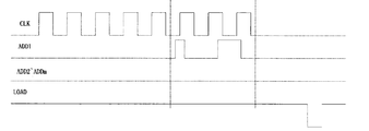
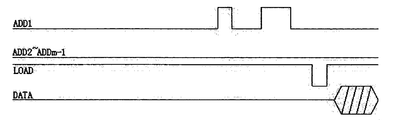
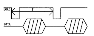
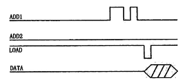
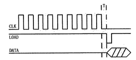
- Figure 2 is a timing diagram of the valid read data command sent by the printer.
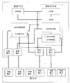
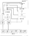
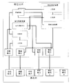
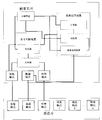
- Figure 3 is a diagram of an ink cartridge system.
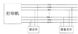
- FIG. 4 is a schematic diagram showing the electrical connection between the repair chip and the original chip and the printer in the first embodiment.
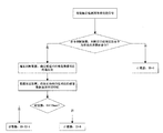
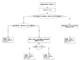
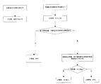
- FIG. 5 is a flow chart of repairing a chip in the first embodiment.
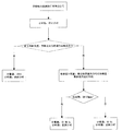
- FIG. 6 is a schematic diagram of the judgment of the printer command in the first embodiment.
- Figure 7 is a diagram of the ink cartridge system in the second embodiment.
- FIG. 8 is a schematic diagram showing the electrical connection between the repair chip and the original chip and the printer in the second embodiment.
- Figure 9 is a flow chart of repairing the chip in the second embodiment.
- FIG. 10 is a schematic diagram of the judgment of the printer command in the second embodiment.
- Figure 11 is a diagram of the ink cartridge system in the third embodiment.
- FIG. 12 is a schematic diagram showing the electrical connection between the repair chip and the original chip and the printer in the third embodiment.
- Figure 13 is a flow chart of the repair chip in the third embodiment.
- Fig. 14 is a schematic diagram showing the judgment of the printer command in the third embodiment.
- Figure 15 is a diagram of the ink cartridge system of the fourth embodiment.
- FIG. 16 is a schematic diagram showing the electrical connection between the repair chip and the original chip and the printer in the fourth embodiment.
- Figure 17 is a flow chart of the repair chip in the fourth embodiment.
- Fig. 18 is a schematic diagram showing the judgment of the printer command in the fourth embodiment.
- the original chip of the ink cartridge is provided with an enable contact, a data contact, an address contact and a clock contact respectively electrically connected to an enable line, a data line, an address line and a clock line of the printer.
- the ink cartridge is installed on the printer, the clock contact of the original chip of the ink cartridge is electrically connected with the clock line of the printer, the enable contact of the original chip is electrically connected with the enable line of the printer, and the data contact of the original chip is electrically connected with the data line of the printer.
- the m address contacts of the original chip are electrically connected to the m address lines of the printer one by one. As shown in FIG.
- the data communication between the ink cartridge and the printer adopts a serial communication mode, and the clock line CLK, the enable line LOAD, and the data line DATA are shared, and the address lines ADD1 to ADDm are used separately.
- Each address line corresponds to a block address of the original chip.
- the clock signal sent by the external printer is used as the sampling clock, and the address lines are respectively sampled on the rising and falling edges of the clock.
- Figure 2 shows the valid read data command sent by the printer: there is only one address line (ADD1) with high and low level changes, and the remaining address lines (ADD2 ⁇ ADDm) remain low.
- the printer selects the block address corresponding to the address line ADD1, and the repair chip samples and decodes the signal appearing on the address line ADD1.
- the data corresponding to the address value sampled and decoded in the block address corresponding to the address line ADD1 is returned to the printer through the data line DATA.
- the printer when the printer sends a valid read data command, it is combined by the signal line CLK, the address line ADD1-m, and the enable line LOAD. Using the association characteristics between certain signal lines of the printer during communication, correctly determine whether the printer command is a valid read data command, and automatically confirm the current memory address to be operated, and take out the corresponding repair data in the corresponding memory address. Return to the printer through the printer's data cable.
- the repair chip is provided with an enable contact, a data contact and an address contact.
- the number of address contacts is one less than the number of printer address lines. It is assumed that the number of address lines of the printer is m, and the number of address contacts of the original chip is m. Fix the number of chip address contacts to m-1.
- Figure 3 repair core
- the sheet is provided with a storage device, a command judging device and a data return device.
- the storage device stores repair data, and the data return device is electrically connected to the address contact, the data contact and the enable contact, respectively, and the data return device and the command judging device are electrically connected. connection.
- the command judging device sets a command judging unit, and the command judging unit is electrically connected with the m-1 address contacts, and is monitored according to the address contact when the enable contact monitors the valid enable signal on the trigger enable line of the printer.
- the signal on the printer's address line determines the printer's command type.
- the data return device is electrically connected to the command determining device, and the data return device is electrically connected to the storage device.
- the data return means includes an address judging means, a data transmitting means, a comparator and a counter.
- the address judging means includes an address block memory for storing a one-to-one correspondence between the printer address lines and the address blocks.
- the waste ink cartridge to be regenerated includes an ink cartridge body and a original chip mounted on the ink cartridge body, and the repair chip is mounted on the ink cartridge body, so that the enable contact of the repair chip is electrically connected with the enable contact of the original chip;
- the data contact is electrically connected to the data contact of the original chip;
- the address contact of the repair chip is electrically connected to any m-1 of the m address contacts of the original chip.
- the remanufactured ink cartridge with the repair chip is mounted on the printer, and the enable contact of the repair chip is electrically connected to the enable line of the printer to monitor the signal on the printer enable line; the data contact of the repair chip is repaired.
- the printer's data line is electrically connected to transmit data through the data line and the printer; the m-1 address contacts of the repair chip are electrically connected to the printer's m-1 address lines to monitor the printer's m-1 address line. signal.
- the storage device of the repair chip stores repair data for making the information indicating the remaining ink amount of the ink cartridge of the ink cartridge not zero.
- the repair data is stored in m address blocks of the storage device that correspond one-to-one with the printer address lines. Each address block stores a certain amount of repair data, and each address block sets the data index maximum value IDmax to indicate the amount of repair data it stores.
- the repair chip monitors the enable line and the address line of the printer by enabling the contact and the address contact, and determines whether the command sent by the printer is a valid read data command by the command judging device, and the data transmitting device of the repair chip judges the printer at the command judging device.
- the address determining device searches for the address block where the repaired data needs to be returned, and finds the storage address of the repair data in the address block according to the data index value; printer.
- the information indicating the remaining ink amount of the ink cartridge of the ink cartridge obtained by the printer is not 0, and the ink cartridge can be used continuously.
- the enable contact monitors the signal on the printer enable line
- the command judging device of the repair chip is electrically connected with the enable contact
- the command judging device detects the valid enable signal when the enable contact is detected, and the start command judging unit judges the printer.
- the type of command is the case in which the enable contact is detected.
- the command judging unit judges the printer command type as shown in Fig. 6: if there is at most one of m-1 address contacts If the address contact detects that there is a signal on the corresponding address line, it determines that the command sent by the printer is a valid read data command; otherwise, it determines that the command sent by the printer is not a valid read data command.
- the data returning device is electrically connected to the command judging unit, and the data returning device and the address judging device are electrically connected.
- the command judging unit judges that the command sent by the printer is a valid read data command
- the address judging device determines the address block where the repair data to be returned is located. :
- the address block memory stores a one-to-one correspondence between the printer address line and the address block. If the address contact does not detect a signal on the m-1 address line of the printer, the address determining device determines that the address block in which the repair data needs to be returned is the address block in the address block memory corresponding to the address line not monitored by the repair chip. Address block; if the address contact detects that there is one signal in the m-1 address line of the printer and only one address line has a signal, the address determining device determines that the address block in which the repair data needs to be returned is: the address block memory has a signal The address block corresponding to the address line.
- the data transmitting unit searches for the repair data stored in the address corresponding to the ID value (data index value) in the corresponding address block, and transmits the data line transmitted through the printer to the printer via the data contact.
- the information indicating the remaining ink amount of the ink cartridge of the ink cartridge obtained by the printer is not zero, that is, the printer thinks that the ink in the ink cartridge is not exhausted.
- the comparator compares the ID value (data index value) with the IDmax value of the corresponding address block (data index maximum):
- the counter sets the ID value to the initial value of zero.
- the counter sets the ID value to the initial value of zero.
- the clock line and all the address lines can be omitted, and only the enable line and the data line are used.
- the repair chip only sets the enable and data contacts.
- the repair chip is provided with a storage device, a command judging device, a data return device, and a timer.
- the storage device stores repair data for making the information indicating the remaining ink amount of the ink cartridge of the ink cartridge not zero.
- the data return device includes a data transmitting device, a comparator, and a counter.
- the waste ink cartridge to be regenerated includes an ink cartridge body and a original chip mounted on the ink cartridge body.
- the repair chip is mounted on the ink cartridge body such that the enable contact of the repair chip is electrically connected to the enable contact of the original chip; the data contact of the repair chip is electrically connected to the data contact of the original chip.
- the remanufactured ink cartridge with the repair chip is mounted on the printer, and the enable contact of the repair chip is electrically connected to the enable line of the printer to monitor the signal on the printer enable line; the data contact of the repair chip is repaired.
- the printer's data line is electrically connected to transfer data to and from the printer via the data line.
- the timer of the repair chip is electrically connected to the enable contact to monitor The printer enables the signal on the line and calculates the time interval between two adjacent valid enable signals on the printer enable line.
- the command judging device is electrically connected to the timer, and the command judging device sets a comparator.
- the comparator is electrically connected to the timer, and determines the command type of the printer according to the time interval at which two adjacent valid enable signals appear on the printer enable line.
- the data return device of the repair chip is electrically connected to the storage device, and the data return device is electrically connected to the command judging device.
- the command judging device judges that the command sent by the printer is a valid read data command, the data is repaired in a predetermined order and by repairing the chip.
- the contacts return all or part of the repair data to the printer via the printer's data line.
- the chip Since the enable contact monitors the first valid enable signal on the enable line, the chip cannot calculate the time interval between the two adjacent valid enable signals on the enable line by the timer to determine the printer command. Type, so in this case the repair chip will return directly to the first order of the repair data that should be returned to the printer.
- the repair chip sets the first effective enable signal judging device.
- the first effective enable signal judging device is electrically connected to the enable contact to determine whether the valid enable signal is the first valid enable signal when the enable contact monitors a valid enable signal on the printer enable line.
- the repair chip monitors the enable line of the printer by enabling the contact, and the command judging device judges whether the command sent by the printer is a valid read data command, and the data transmitting device of the repair chip determines that the command sent by the printer is a valid read at the command judging device.
- the data is commanded, all or part of the repair data is sent to the printer through the data transmitting device in a predetermined order.
- the information indicating the remaining ink amount of the ink cartridge of the ink cartridge obtained by the printer is not 0, and the ink cartridge can be used continuously.
- the enable contact monitors the signal on the printer enable line and the timer stops when the enable contact detects a valid enable signal.
- the timer value at this time represents the time interval T between two adjacent valid enable signals on the printer, as shown in FIG.
- the first effective enable signal judging device of the repair chip is electrically connected with the enable contact.
- the memory device of the repair chip stores a Flag flag (first enable signal flag, and the mark repair chip has received a valid enable signal; Flag is true) , indicating that the repair chip has not received a valid enable signal; Flag is false, indicating that the repair chip has received a valid enable signal.
- the initial value of Flag is true).
- the first effective enable signal judging device acquires the value of the Flag flag in the storage device when the enable contact monitors a valid enable signal on the printer: if Flag is true, it determines that the enable contact is effectively enabled.
- the signal is the first valid enable signal; if Flag is false, it is determined that the valid enable signal monitored by the enable contact is not the first valid enable signal.
- the data return device is electrically connected to the first effective enable signal determining device.
- the data return device stores the device in the ID The value (data index value, one-to-one correspondence with the repair data stored in the storage device, the initial value is 0 and the repair data is marked in a predetermined order), and the repair data corresponding to the repair data is returned to the data line of the printer through the data contact to printer.
- the command judging device is electrically connected to the first valid enable signal judging device.
- the command judging device judges the command sent by the printer. Is it a valid read data command:
- the comparator of the command judging device is electrically connected to the timer, and the comparator compares the time interval T with the preset time interval maximum value Tmax and the time interval minimum value Tmin: if T>Tmax or T ⁇ Tmin, the command judging device judges that the printer sends The command is not a valid read data command; if Tmin ⁇ T ⁇ Tmax, the command judging device judges that the command sent by the printer is a valid read data command.
- the data returning device is electrically connected to the command determining device.
- the command determining device determines that the command sent by the printer is a valid read data command
- the repair chip sets the Flag value in the storage device to false, and the ID value is set to an initial value of 0; the timer restarts timing.
- the clock line and one or more address lines can be omitted.
- Repair chip setup enable contacts, data contacts, and 2 address contacts.
- the repair chip is provided with a storage device, a command judging device, a data return device, and a timer.
- the storage device stores repair data for making the information indicating the remaining ink amount of the ink cartridge of the ink cartridge not zero.
- the waste ink cartridge to be regenerated includes an ink cartridge body and a original chip mounted on the ink cartridge body. Mounting the repair chip on the ink cartridge body, so that the enable contact of the repair chip is electrically connected with the enable contact of the original chip; the data contact of the repair chip is electrically connected with the data contact of the original chip, and the two addresses of the repair chip are repaired.
- the contacts are electrically connected to any two address contacts of the original chip.
- the remanufactured ink cartridge with the repair chip is mounted on the printer, and the enable contact of the repair chip is electrically connected to the enable line of the printer to monitor the signal on the printer enable line; repair the data contacts of the chip and Printer data cable Electrically connected to transmit data through the data line to the printer; the two address contacts of the repair chip are electrically connected to the two address lines of the printer.
- the repair chip's timer is electrically coupled to the enable contact to monitor the signal on the printer enable line and calculate the time interval between two adjacent valid enable signals on the printer enable line.
- the command judging device is electrically connected to the timer, and the command judging device is electrically connected to the two address contacts of the repair chip.
- the command judging device sets a comparator and a command judging unit, and the comparator is electrically connected to the timer, and the command judging unit is electrically connected to the two address contacts of the repair chip.
- the command judging device comprehensively judges the command type of the printer according to the time interval of occurrence of the adjacent two effective enable signals on the printer enable line and the signal on the address line.
- the data return device of the repair chip is electrically connected to the storage device, and the data return device is electrically connected to the command judging device.
- the repair chip monitors the enable line of the printer by enabling the contact, and the command judging device judges whether the command sent by the printer is a valid read data command, and the data transmitting device of the repair chip determines that the command sent by the printer is a valid read at the command judging device.
- the data is commanded, all or part of the repair data is sent to the printer through the data transmitting device in a predetermined order.
- the information indicating the remaining ink amount of the ink cartridge of the ink cartridge obtained by the printer is not 0, and the ink cartridge can be used continuously.
- the enable contact monitors the signal on the printer enable line and the timer stops when the enable contact detects a valid enable signal.
- the timer value at this time represents the time interval T between two adjacent valid enable signals on the printer, as shown in FIG.
- the command judging means when the enable contact detects a valid enable signal, the start command judging unit and the comparator comprehensively judge the command type of the printer:
- the command judging unit judges that at most one of the address contacts of the repair chip detects that there is a signal on the corresponding address line, and the comparator compares the time interval T with the preset time interval maximum value Tmax and the minimum time interval The result of Tmin is: Tmin ⁇ T ⁇ Tmax, the command judging means judges that the command sent by the printer is a valid read data command. Otherwise, the command judging means judges that the command sent by the printer is not a valid read data command.
- the data returning device is electrically connected to the command determining device.
- the command determining device determines that the command sent by the printer is a valid read data command
- the ID value is set to the initial value of 0; the timer restarts.
- the repair chip sets the ID value in the storage device to the initial value of 0; the timer restarts timing.
- all address lines can be used, and only clock lines, enable lines, and data lines are used.
- the repair chip only sets the clock contacts, enable contacts, and data contacts.
- the repair chip is provided with a storage device, a command judging device, a data return device, and a timer.
- the storage device stores repair data for making the information indicating the remaining ink amount of the ink cartridge of the ink cartridge not zero.
- the waste ink cartridge to be regenerated includes an ink cartridge body and a original chip mounted on the ink cartridge body.
- the repair chip is mounted on the ink cartridge body, so that the clock of the repair chip is electrically connected to the clock of the original chip; the enable contact of the repair chip is electrically connected with the enable contact of the original chip; and the data contact of the repair chip is repaired.
- the data contacts of the chip are electrically connected.
- the remanufactured ink cartridge with the repair chip is mounted on the printer, and the clock contact of the repair chip is electrically connected to the clock line of the printer to monitor the clock signal on the print clock line; the enable contact of the repair chip and the printer are repaired.
- the enable line is electrically connected to monitor the signal on the printer enable line; the data contact of the repair chip is electrically coupled to the printer's data line for data transfer to the printer via the data line.
- the repair chip's timer is electrically coupled to the enable contact and the clock contact to monitor the active enable signal on the printer enable line and the clock signal on the printer's clock line, and to calculate the effective enable on the printer enable line. The time interval between the signal and the last clock signal present on the clock line.
- the command judging device is electrically connected to the timer, the command judging device sets the comparator, the comparator is electrically connected to the timer, and the printer is determined according to the time interval between the valid enable signal on the printer enable line and the last clock signal on the printer clock line.
- the type of command is electrically connected to the data return device of the repair chip is electrically connected to the storage device, and the data return device is electrically connected to the command judging device.
- the clock contact monitors the signal on the printer's clock line.
- the repair chip clears the timer parameter and restarts timing.
- the enable contact monitors the signal on the printer enable line and the timer stops when the enable contact detects a valid enable signal.
- the timer value at this time represents the time interval T between the valid enable signal on the printer enable line and the last clock signal on the printer clock line, as shown in Figure 18.
- the command judging device is electrically connected to the enable contact.
- the enable contact detects a valid enable signal
- the command judging device judges whether the command sent by the printer is a valid read data command:
- the comparator of the command judging device is electrically connected to the timer, and the comparator compares the time interval T with the preset time interval.
- the value Tmax and the time interval minimum value Tmin if T>Tmax or T ⁇ Tmin, the command judging device judges that the command sent by the printer is not a valid read data command; if Tmin ⁇ T ⁇ Tmax, the command judging device judges the command sent by the printer For valid read data commands.
- the data returning device is electrically connected to the command determining device.
- the command determining device determines that the command sent by the printer is a valid read data command
- the ID value is set to the initial value of 0.
- the repair chip sets the ID value in the storage device to the initial value of zero.
Landscapes
- Engineering & Computer Science (AREA)
- Physics & Mathematics (AREA)
- General Physics & Mathematics (AREA)
- Computer Vision & Pattern Recognition (AREA)
- Theoretical Computer Science (AREA)
- Manufacturing & Machinery (AREA)
- Computer Networks & Wireless Communication (AREA)
- General Engineering & Computer Science (AREA)
- Ink Jet (AREA)
Abstract
L'invention concerne un procédé de réparation et une puce de réparation destinés à une cartouche d'encre remise à neuf, et une cartouche d'encre remise à neuf. Selon les caractéristiques d'un protocole de communication entre la puce d'origine d'une cartouche d'encre et une imprimante, la puce de réparation détermine le type d'une commande envoyée par l'imprimante uniquement selon les caractéristiques de signal d'un petit nombre de circuits d'imprimante surveillés par la puce de réparation ; détermine, uniquement selon des signaux relatifs au petit nombre de circuits d'imprimante surveillés par la puce de réparation, les données devant être obtenues par l'imprimante lorsqu'il est déterminé que la commande envoyée par l'imprimante est une commande valide de lecture de données, et renvoie les données à l'imprimante au moyen d'une ligne de données de l'imprimante. La puce de réparation n'a pas besoin de surveiller tous les circuits d'une imprimante, et ne doit surveiller qu'une ligne de validation et une ligne de données de l'imprimante, ainsi que de 0 à (n-1) lignes auxiliaires, ce qui permet de réduire le nombre des contacts électriquement connectés à l'imprimante et à la puce d'origine, ainsi que la difficulté de soudage et les charges de travail lors d'un processus de remise à neuf d'une cartouche d'encre et de réduire, à partir de la source, le risque d'endommagement de la cartouche d'encre au cours d'un processus de réparation.
Priority Applications (3)
| Application Number | Priority Date | Filing Date | Title |
|---|---|---|---|
| PCT/CN2015/098212 WO2017107045A1 (fr) | 2015-12-22 | 2015-12-22 | Procédé de réparation et puce de réparation pour cartouche d'encre remise à neuf, et cartouche d'encre remise à neuf |
| EP15911044.4A EP3395577B1 (fr) | 2015-12-22 | 2015-12-22 | Procédé de réparation et puce de réparation pour cartouche d'encre remise à neuf, et cartouche d'encre remise à neuf |
| US15/749,117 US10372073B2 (en) | 2015-12-22 | 2015-12-22 | Repair method and repair chip for regenerative ink cartridge, and regenerative ink cartridge |
Applications Claiming Priority (1)
| Application Number | Priority Date | Filing Date | Title |
|---|---|---|---|
| PCT/CN2015/098212 WO2017107045A1 (fr) | 2015-12-22 | 2015-12-22 | Procédé de réparation et puce de réparation pour cartouche d'encre remise à neuf, et cartouche d'encre remise à neuf |
Publications (1)
| Publication Number | Publication Date |
|---|---|
| WO2017107045A1 true WO2017107045A1 (fr) | 2017-06-29 |
Family
ID=59088858
Family Applications (1)
| Application Number | Title | Priority Date | Filing Date |
|---|---|---|---|
| PCT/CN2015/098212 Ceased WO2017107045A1 (fr) | 2015-12-22 | 2015-12-22 | Procédé de réparation et puce de réparation pour cartouche d'encre remise à neuf, et cartouche d'encre remise à neuf |
Country Status (3)
| Country | Link |
|---|---|
| US (1) | US10372073B2 (fr) |
| EP (1) | EP3395577B1 (fr) |
| WO (1) | WO2017107045A1 (fr) |
Cited By (3)
| Publication number | Priority date | Publication date | Assignee | Title |
|---|---|---|---|---|
| CN111376609A (zh) * | 2018-12-29 | 2020-07-07 | 珠海纳思达企业管理有限公司 | 墨盒回收方法及回收墨盒 |
| CN111746133A (zh) * | 2020-06-11 | 2020-10-09 | 杭州旗捷科技有限公司 | 再生芯片的控制方法、再生芯片和再生墨盒 |
| CN120116619A (zh) * | 2025-03-26 | 2025-06-10 | 广东智慧机电设备有限公司 | 一种墨盒芯片直接复位装置及方法 |
Families Citing this family (9)
| Publication number | Priority date | Publication date | Assignee | Title |
|---|---|---|---|---|
| CN109968837B (zh) * | 2018-09-28 | 2020-11-20 | 珠海艾派克微电子有限公司 | 打印耗材及耗材再生方法 |
| CN109291647A (zh) * | 2018-11-09 | 2019-02-01 | 北海绩迅电子科技有限公司 | 一种墨盒加工方法及改进墨盒 |
| CN211942586U (zh) * | 2019-12-13 | 2020-11-17 | 杭州旗捷科技有限公司 | 修复芯片、墨盒和打印机 |
| CN111737164B (zh) * | 2019-12-31 | 2024-07-23 | 极海微电子股份有限公司 | 访问请求响应方法、耗材芯片以及存储介质 |
| US11977343B2 (en) | 2021-04-22 | 2024-05-07 | Zhuhai Pantum Electronics Co., Ltd. | Consumable chip, consumable and communication method |
| CN113138548B (zh) * | 2021-04-22 | 2022-11-01 | 珠海奔图电子有限公司 | 图像形成装置、耗材芯片、耗材及通信方法 |
| CN114326526B (zh) * | 2021-12-31 | 2023-07-07 | 福建新大陆支付技术有限公司 | 自动售货机、指令解析方法、存储介质及其从设备 |
| CN116061582B (zh) * | 2022-12-30 | 2025-10-10 | 极海微电子股份有限公司 | 一种控制芯片、控制方法及耗材盒 |
| CN116552129B (zh) * | 2023-05-10 | 2026-03-24 | 杭州旗捷科技股份有限公司 | 一种原装耗材回收重利用方法、芯片、耗材及存储介质 |
Citations (9)
| Publication number | Priority date | Publication date | Assignee | Title |
|---|---|---|---|---|
| EP0789322A2 (fr) * | 1996-01-08 | 1997-08-13 | Hewlett-Packard Company | Pièce de rechange à mémoire intégrée pour des données d'usage, de calibration et autres |
| JP2004098564A (ja) * | 2002-09-11 | 2004-04-02 | S T Sangyo Kk | 使用済みインクカートリッジのための再利用化用具 |
| CN1814451A (zh) * | 2005-02-02 | 2006-08-09 | 精工爱普生株式会社 | 印刷装置的内部控制 |
| CN1991633A (zh) * | 2005-12-28 | 2007-07-04 | 帕克&Opc株式会社 | 用于修复墨盒的微型芯片与方法 |
| CN101941330A (zh) * | 2010-08-26 | 2011-01-12 | 珠海天威技术开发有限公司 | 打印机固件的修改方法 |
| CN104070824A (zh) * | 2014-05-16 | 2014-10-01 | 珠海艾派克微电子有限公司 | 一种带喷头墨盒及其修复方法、喷墨成像设备 |
| CN204472118U (zh) * | 2015-02-02 | 2015-07-15 | 珠海艾派克微电子有限公司 | 修复芯片、墨盒和打印机 |
| CN105398226A (zh) * | 2015-12-22 | 2016-03-16 | 杭州旗捷科技有限公司 | 再生墨盒的修复方法、修复芯片和再生墨盒 |
| CN205238874U (zh) * | 2015-12-22 | 2016-05-18 | 杭州旗捷科技有限公司 | 修复芯片和再生墨盒 |
Family Cites Families (7)
| Publication number | Priority date | Publication date | Assignee | Title |
|---|---|---|---|---|
| JPH04371965A (ja) * | 1991-06-20 | 1992-12-24 | Canon Inc | リサイクル使用可能なカートリッジ及び該カートリッジを装着可能な装置 |
| JP4395943B2 (ja) * | 1998-11-26 | 2010-01-13 | セイコーエプソン株式会社 | 印刷装置およびその情報の管理方法 |
| JP4995562B2 (ja) * | 2006-12-25 | 2012-08-08 | 株式会社リコー | 画像形成装置 |
| JP5151372B2 (ja) * | 2007-10-01 | 2013-02-27 | セイコーエプソン株式会社 | 液体噴射装置、および、液体噴射装置の制御方法 |
| US8764172B2 (en) * | 2010-09-03 | 2014-07-01 | Seiko Epson Corporation | Printing apparatus, printing material cartridge, adaptor for printing material container, and circuit board |
| US8737849B2 (en) * | 2011-05-02 | 2014-05-27 | Static Control Components, Inc. | Addressing for a memory device used in an image recording apparatus |
| CN103085487B (zh) * | 2011-11-04 | 2015-04-22 | 珠海艾派克微电子有限公司 | 一种带自适应触点的成像盒芯片、成像盒及其自适应方法 |
-
2015
- 2015-12-22 EP EP15911044.4A patent/EP3395577B1/fr active Active
- 2015-12-22 US US15/749,117 patent/US10372073B2/en active Active
- 2015-12-22 WO PCT/CN2015/098212 patent/WO2017107045A1/fr not_active Ceased
Patent Citations (9)
| Publication number | Priority date | Publication date | Assignee | Title |
|---|---|---|---|---|
| EP0789322A2 (fr) * | 1996-01-08 | 1997-08-13 | Hewlett-Packard Company | Pièce de rechange à mémoire intégrée pour des données d'usage, de calibration et autres |
| JP2004098564A (ja) * | 2002-09-11 | 2004-04-02 | S T Sangyo Kk | 使用済みインクカートリッジのための再利用化用具 |
| CN1814451A (zh) * | 2005-02-02 | 2006-08-09 | 精工爱普生株式会社 | 印刷装置的内部控制 |
| CN1991633A (zh) * | 2005-12-28 | 2007-07-04 | 帕克&Opc株式会社 | 用于修复墨盒的微型芯片与方法 |
| CN101941330A (zh) * | 2010-08-26 | 2011-01-12 | 珠海天威技术开发有限公司 | 打印机固件的修改方法 |
| CN104070824A (zh) * | 2014-05-16 | 2014-10-01 | 珠海艾派克微电子有限公司 | 一种带喷头墨盒及其修复方法、喷墨成像设备 |
| CN204472118U (zh) * | 2015-02-02 | 2015-07-15 | 珠海艾派克微电子有限公司 | 修复芯片、墨盒和打印机 |
| CN105398226A (zh) * | 2015-12-22 | 2016-03-16 | 杭州旗捷科技有限公司 | 再生墨盒的修复方法、修复芯片和再生墨盒 |
| CN205238874U (zh) * | 2015-12-22 | 2016-05-18 | 杭州旗捷科技有限公司 | 修复芯片和再生墨盒 |
Cited By (7)
| Publication number | Priority date | Publication date | Assignee | Title |
|---|---|---|---|---|
| CN111376609A (zh) * | 2018-12-29 | 2020-07-07 | 珠海纳思达企业管理有限公司 | 墨盒回收方法及回收墨盒 |
| CN111376609B (zh) * | 2018-12-29 | 2021-04-20 | 珠海纳思达企业管理有限公司 | 墨盒回收方法及回收墨盒 |
| CN111746133A (zh) * | 2020-06-11 | 2020-10-09 | 杭州旗捷科技有限公司 | 再生芯片的控制方法、再生芯片和再生墨盒 |
| CN111746133B (zh) * | 2020-06-11 | 2021-11-16 | 杭州旗捷科技有限公司 | 再生芯片的控制方法、再生芯片和再生墨盒 |
| WO2021248990A1 (fr) * | 2020-06-11 | 2021-12-16 | 杭州旗捷科技有限公司 | Procédé de commande de puce régénérée, puce régénérée et cartouche d'encre régénérée |
| US12128687B2 (en) | 2020-06-11 | 2024-10-29 | Hangzhou Chipjet Technology Co., Ltd. | Method for controlling regenerated chip, regenerated chip and regenerated ink cartridge |
| CN120116619A (zh) * | 2025-03-26 | 2025-06-10 | 广东智慧机电设备有限公司 | 一种墨盒芯片直接复位装置及方法 |
Also Published As
| Publication number | Publication date |
|---|---|
| US20180224787A1 (en) | 2018-08-09 |
| EP3395577A1 (fr) | 2018-10-31 |
| EP3395577A4 (fr) | 2019-03-13 |
| US10372073B2 (en) | 2019-08-06 |
| EP3395577B1 (fr) | 2023-09-27 |
Similar Documents
| Publication | Publication Date | Title |
|---|---|---|
| WO2017107045A1 (fr) | Procédé de réparation et puce de réparation pour cartouche d'encre remise à neuf, et cartouche d'encre remise à neuf | |
| CN105398226B (zh) | 再生墨盒的修复方法、修复芯片和再生墨盒 | |
| CN205238874U (zh) | 修复芯片和再生墨盒 | |
| CN102627033B (zh) | 存储芯片及其复位方法、耗材容器、成像设备 | |
| US20230231938A1 (en) | EtherCAT Device | |
| CN111459557A (zh) | 一种缩短服务器开机时间的方法及系统 | |
| CN106648016B (zh) | 供电电路、供电设备及供电方法 | |
| CN201859389U (zh) | 一种复位管理芯片及复位系统 | |
| CN116340073B (zh) | 测试方法、装置及系统 | |
| CN104442010A (zh) | 修复芯片、墨盒、打印机及修复芯片连接稳定性检测方法 | |
| CN106649158B (zh) | 通过i2c接口读写内部寄存器堆的装置及方法 | |
| CN204296206U (zh) | 修复芯片、墨盒和打印机 | |
| US8423809B2 (en) | Power consumption measuring and power transmission monitoring for data transfer | |
| CN201562208U (zh) | 一种刀片服务器的存储扩展卡 | |
| CN115027390A (zh) | 车辆下电时间计算方法、装置及电子设备、存储介质 | |
| CN105354157A (zh) | 配置iic器件的方法、装置和系统 | |
| CN207825743U (zh) | 再生芯片 | |
| CN201037900Y (zh) | 成像盒芯片 | |
| CN108549042B (zh) | 一种nvme led检测系统及检测方法 | |
| CN115914327B (zh) | 一种控制方法、装置、设备及存储介质 | |
| CN202517844U (zh) | 存储芯片、耗材容器、成像设备 | |
| CN206282267U (zh) | 一种计算机故障报警系统 | |
| CN104202191A (zh) | 故障指示器远传通信终端与主站通信工作模式的切换方法 | |
| US20180335817A1 (en) | Data storage system and external power supply module capable of providing a standby power | |
| CN216388754U (zh) | 一种具有自检功能的固态硬盘及存储设备 |
Legal Events
| Date | Code | Title | Description |
|---|---|---|---|
| 121 | Ep: the epo has been informed by wipo that ep was designated in this application |
Ref document number: 15911044 Country of ref document: EP Kind code of ref document: A1 |
|
| WWE | Wipo information: entry into national phase |
Ref document number: 15749117 Country of ref document: US |
|
| NENP | Non-entry into the national phase |
Ref country code: DE |