WO2017107938A1 - Procédé, appareil et système de modulation par multiplexage chevauché - Google Patents
Procédé, appareil et système de modulation par multiplexage chevauché Download PDFInfo
- Publication number
- WO2017107938A1 WO2017107938A1 PCT/CN2016/111405 CN2016111405W WO2017107938A1 WO 2017107938 A1 WO2017107938 A1 WO 2017107938A1 CN 2016111405 W CN2016111405 W CN 2016111405W WO 2017107938 A1 WO2017107938 A1 WO 2017107938A1
- Authority
- WO
- WIPO (PCT)
- Prior art keywords
- envelope waveform
- waveform
- modulation
- envelope
- sequence
- Prior art date
- Legal status (The legal status is an assumption and is not a legal conclusion. Google has not performed a legal analysis and makes no representation as to the accuracy of the status listed.)
- Ceased
Links
Images






Classifications
-
- H—ELECTRICITY
- H04—ELECTRIC COMMUNICATION TECHNIQUE
- H04J—MULTIPLEX COMMUNICATION
- H04J4/00—Combined time-division and frequency-division multiplex systems
-
- H—ELECTRICITY
- H04—ELECTRIC COMMUNICATION TECHNIQUE
- H04J—MULTIPLEX COMMUNICATION
- H04J1/00—Frequency-division multiplex systems
- H04J1/02—Details
- H04J1/06—Arrangements for supplying the carrier waves ; Arrangements for supplying synchronisation signals
-
- H—ELECTRICITY
- H04—ELECTRIC COMMUNICATION TECHNIQUE
- H04J—MULTIPLEX COMMUNICATION
- H04J14/00—Optical multiplex systems
- H04J14/08—Time-division multiplex systems
-
- H—ELECTRICITY
- H04—ELECTRIC COMMUNICATION TECHNIQUE
- H04J—MULTIPLEX COMMUNICATION
- H04J3/00—Time-division multiplex systems
- H04J3/02—Details
- H04J3/04—Distributors combined with modulators or demodulators
-
- H—ELECTRICITY
- H04—ELECTRIC COMMUNICATION TECHNIQUE
- H04J—MULTIPLEX COMMUNICATION
- H04J3/00—Time-division multiplex systems
- H04J3/16—Time-division multiplex systems in which the time allocation to individual channels within a transmission cycle is variable, e.g. to accommodate varying complexity of signals, to vary number of channels transmitted
- H04J3/1676—Time-division multiplex with pulse-position, pulse-interval, or pulse-width modulation
-
- H—ELECTRICITY
- H04—ELECTRIC COMMUNICATION TECHNIQUE
- H04J—MULTIPLEX COMMUNICATION
- H04J99/00—Subject matter not provided for in other groups of this subclass
-
- H—ELECTRICITY
- H04—ELECTRIC COMMUNICATION TECHNIQUE
- H04L—TRANSMISSION OF DIGITAL INFORMATION, e.g. TELEGRAPHIC COMMUNICATION
- H04L5/00—Arrangements affording multiple use of the transmission path
- H04L5/22—Arrangements affording multiple use of the transmission path using time-division multiplexing
-
- H—ELECTRICITY
- H04—ELECTRIC COMMUNICATION TECHNIQUE
- H04L—TRANSMISSION OF DIGITAL INFORMATION, e.g. TELEGRAPHIC COMMUNICATION
- H04L27/00—Modulated-carrier systems
- H04L27/0006—Assessment of spectral gaps suitable for allocating digitally modulated signals, e.g. for carrier allocation in cognitive radio
-
- H—ELECTRICITY
- H04—ELECTRIC COMMUNICATION TECHNIQUE
- H04L—TRANSMISSION OF DIGITAL INFORMATION, e.g. TELEGRAPHIC COMMUNICATION
- H04L27/00—Modulated-carrier systems
- H04L27/18—Phase-modulated carrier systems, i.e. using phase-shift keying
- H04L27/24—Half-wave signalling systems
Definitions
- the present invention relates to the field of communications, and in particular, to an overlapping multiplexing modulation method, apparatus, and overlapping multiplexing system.
- Time Division Multiplexing is a technique for sharing a plurality of signal symbols occupying a narrow time duration in a digital communication for a wide time duration.
- Frequency Division Multiplexing is a technology that allows multiple signals occupying a narrow bandwidth to share a wider bandwidth.
- the used signal bandwidths are B1, B2, B3, B4, ...., of course, they can also occupy the same bandwidth, ⁇ B is the minimum protection bandwidth, and the actual protection bandwidth can be a little more.
- ⁇ B should be greater than the transition bandwidth of the demultiplexing filter used plus the maximum frequency drift of the system and the maximum frequency spread of the channel. This is the most common frequency division multiplexing technology, and most of the existing broadcasting systems, communication systems, and radar systems use this technology. The biggest feature of this technology is that the used signal spectrums are isolated from each other without mutual interference.
- FIG. 1A is a schematic diagram of a conventional time division multiplexing technique; the time duration of each multiplexed signal symbol in FIG. 1A (called time slot width in engineering) is T1, T2, T3, T4, .. In engineering, they are usually allowed to occupy the same time slot width, ⁇ T is the minimum protection time slot, and the actual protection time slot width should be a bit more. ⁇ T should be greater than the transition time width of the demultiplexed gate used plus the maximum amount of time jitter of the system. This is the most common time division multiplexing technique. Most of the existing multi-channel digital broadcasting systems and multi-channel digital communication systems use this technology.
- FIG. 1B corresponds to a schematic diagram of a frequency division multiplexing technique.
- the used signal bandwidths are B1, B2, B3, B4, ...., of course, they can also occupy the same bandwidth, ⁇ B is the minimum protection bandwidth, and the actual protection bandwidth can be a little more.
- ⁇ B should be greater than the transition bandwidth of the demultiplexing filter used plus the maximum frequency drift of the system and the maximum frequency spread of the channel. This is the most common frequency division multiplexing technology, and most of the existing broadcasting systems, communication systems, and radar systems use this technology. The biggest feature of this technology is that the used signal spectrums are isolated from each other without mutual interference.
- the most important feature of this technology when applied to digital communication is that the multiplexed signal symbols are completely isolated from each other in time, and there is never mutual interference. There is no restriction on the multiplexed signal symbols, and the symbols of the respective signals.
- the duration (slot width) can have different widths, and can also be applied to different communication systems, as long as their time slots do not overlap each other, and thus are most widely used. But with this multiplexing, multiplexing itself has no effect on improving the spectral efficiency of the system.
- the conventional view is that adjacent channels do not overlap in the time domain to avoid interference between adjacent channels, but this technique restricts the improvement of spectral efficiency.
- the prior art time division multiplexing technology has the view that the channels do not need to be isolated from each other, and can have strong mutual overlap, as shown in FIG. 2A.
- the prior art considers the overlap between channels as a new coding constraint relationship, and proposes a corresponding modulation and demodulation technique according to the constraint relationship, so it is called Overlapped Time Division Multiplexing (OvTDM).
- This technique causes the spectral efficiency to increase proportionally with the number of overlaps K; and in the frequency domain corresponds to Overlapped Frequency Division Multiplexing, which corresponds to FIG. 2B.
- the number of overlaps K can be increased indefinitely, so the spectral efficiency can be increased indefinitely, but in the laboratory research stage, it is found that with the number of overlaps.
- the increase of K although the spectral efficiency is increased, but the transmission power also increases, and the increase of transmission power in turn limits the increase of the number of overlaps K to a certain extent, thereby limiting the increase of spectral efficiency.
- the present application provides an overlapping time division multiplexing modulation method, including:
- the initial envelope waveform is shifted in a time domain according to a predetermined shift interval according to the number of overlapping multiplexing to obtain an offset envelope waveform of the transmitted signal at each moment;
- the modulation envelope waveforms at various times are superimposed in the time domain to obtain a complex modulation envelope waveform carrying the output signal sequence.
- the present application further provides an overlapping time division multiplexing modulation apparatus, including:
- a waveform generating module configured to generate an initial envelope waveform of the waveform smoothing in the time domain according to the design parameter
- a shifting module configured to shift the initial envelope waveform by a predetermined shift interval in the time domain according to the number of overlapping multiplexing, to obtain an offset envelope waveform of the transmitted signal at each moment;
- a modulation module for converting the input digital signal sequence into a sequence of positive and negative symbols
- a multiplication module configured to multiply the input positive and negative symbol sequence by an offset envelope waveform of the signal transmitted at each time after the offset to obtain a modulation envelope waveform at each moment;
- the superposition module is configured to superimpose the modulation envelope waveforms at each moment in the time domain to obtain a complex modulation envelope waveform carrying the output signal sequence.
- an overlapping frequency division multiplexing modulation method comprising the steps of:
- the initial envelope waveform is shifted in a frequency domain according to a predetermined spectral interval according to the number of overlapping multiplexing, to obtain an envelope waveform of each subcarrier;
- the complex modulation envelope waveform in the frequency domain is transformed to obtain a complex modulation envelope waveform in the time domain.
- a fourth aspect of the present invention provides an overlapping frequency division multiplexing modulation apparatus, including:
- a waveform generating module configured to generate an initial envelope waveform of a waveform smoothing in a frequency domain
- a shifting module configured to shift the initial envelope waveform in a frequency domain according to a predetermined spectral interval according to the number of overlapping multiplexing, to obtain an envelope waveform of each subcarrier
- a conversion module for converting the input digital signal sequence into a sequence of positive and negative symbols
- a multiplication module configured to multiply the symbols in the sequence of positive and negative symbols by respective corresponding subcarrier envelope waveforms to obtain a modulation envelope waveform of each subcarrier
- a superimposing module configured to superimpose a modulation envelope waveform of each subcarrier in a frequency domain to obtain a complex modulation envelope waveform in a frequency domain;
- a transform module configured to transform the complex modulation envelope waveform in the frequency domain to obtain a complex modulation envelope waveform in the time domain.
- the overlapping time division multiplexing modulation method, device and system since the time domain waveform of the initial envelope waveform is relatively smooth, the frequency domain bandwidth is narrow, and the superposed waveform is smooth and limited to a narrow bandwidth, thereby improving The spectrum utilization rate and transmission rate of the system reduce the bit error rate of the system; and the overlapping frequency division multiplexing modulation method, device and system, because the generated initial envelope waveform is smooth in the frequency domain, correspondingly, in the time domain
- the energy is concentrated and the duration is short, so the polymodulation envelope waveform formed by its modulation is concentrated in the time domain and has a short duration, so its spectrum utilization is high, the signal transmission rate is also high, and only a low transmission is required. Power, which has a lower bit error rate when demodulated.
- 1A is a schematic diagram of a conventional time division multiplexing technique
- 1B is a schematic diagram of a conventional frequency division multiplexing technique
- 2A is a schematic diagram of the principle of overlapping time division multiplexing
- 2B is a schematic diagram of the principle of overlapping frequency division multiplexing
- 3A is a schematic structural diagram of an overlapping time division multiplexing system according to an embodiment of the present invention.
- FIG. 3B is a schematic structural diagram of an overlapping frequency division multiplexing system according to an embodiment of the present invention
- FIG. 4A is a schematic structural diagram of an overlapping time division multiplexing modulation apparatus according to an embodiment of the present invention
- 4B is a schematic structural diagram of an overlapping frequency division multiplexing modulation apparatus according to an embodiment of the present invention.
- 5A is a schematic diagram showing the hardware structure of an overlapping time division multiplexing modulation apparatus according to an embodiment of the present invention
- 5B is a schematic structural diagram of hardware of an overlapping frequency division multiplexing modulation apparatus according to an embodiment of the present invention.
- FIG. 6 is a schematic structural diagram of a receiver preprocessing apparatus according to an embodiment of the present invention.
- FIG. 7 is a schematic structural diagram of a receiver sequence detecting apparatus according to an embodiment of the present invention.
- FIG. 8 is a time domain waveform and a frequency domain waveform diagram of a Chebyshev envelope waveform according to an embodiment of the present invention.
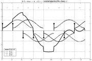
- FIG. 10 is a schematic diagram of superposition of waveforms to be transmitted when a Chebyshev envelope waveform is used in an embodiment of the present invention
- FIG. 11 is a schematic diagram of the principle of K-way waveform multiplexing
- FIG. 12 is a schematic diagram showing the principle of a symbol superposition process of a K-path waveform
- Figure 14 is a node state transition diagram
- Figure 15 is a time-domain and frequency-domain waveform diagram of a rectangular wave
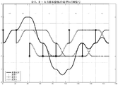
- Figure 16 is a diagram showing each of the signals generated when the rectangular wave envelope waveform is selected by the envelope waveform and the superimposed waveform;
- 17 is a time-domain waveform and a frequency domain waveform diagram of a Blackman first-order derivative envelope waveform according to an embodiment of the present invention.
- FIG. 19 is a schematic diagram showing superposition of waveforms to be transmitted when a Blackman first-order derivative envelope waveform is used in an embodiment of the present invention.
- FIG. 20 is a schematic diagram of superposition of waveforms to be transmitted when a Blackman-Harris first-order derivative envelope waveform is used in an embodiment of the present invention.
- 21 is a time-domain waveform and a frequency domain waveform diagram of a Bartlett envelope waveform in an embodiment of the present invention.
- 22 is an envelope waveform diagram of each time after the Bartlett window is shifted in an embodiment of the present invention.
- FIG. 23 is a schematic diagram showing superposition of waveforms to be transmitted when a Bartlett envelope waveform is used in an embodiment of the present invention.
- 24 is a time domain waveform and a frequency domain waveform diagram of a Gaussian envelope waveform in an embodiment of the present invention.
- 25 is an envelope waveform diagram of each time after a Gaussian window is shifted according to an embodiment of the present invention.
- 26 is a schematic diagram of superposition of waveforms to be transmitted when a Gaussian envelope waveform is used in an embodiment of the present invention
- 27 is a time-domain waveform and a frequency domain waveform diagram of a Hanning envelope waveform in an embodiment of the present invention
- 29 is a schematic diagram showing superposition of waveforms to be transmitted when a Hanning envelope waveform is used in an embodiment of the present invention.
- FIG. 30 is a time-domain waveform and a frequency domain waveform diagram of a Kaiser envelope waveform in an embodiment of the present invention
- FIG. 31 is an envelope waveform diagram of each time after a Kaiser window is shifted according to an embodiment of the present invention.
- 33 is a time-domain waveform and a frequency domain waveform diagram of a Hamming envelope waveform in an embodiment of the present invention.
- FIG. 34 is a diagram showing envelope waveforms of respective moments after a Hamming window is shifted according to an embodiment of the present invention.
- FIG. 35 is a schematic diagram of superposition of waveforms to be transmitted when a Hamming envelope waveform is used in an embodiment of the present invention.
- 36 is a time-domain waveform and a frequency domain waveform diagram of a Bartlett-Hanning envelope waveform in an embodiment of the present invention
- FIG. 38 is a schematic diagram showing superposition of waveforms to be transmitted when a Bartlett-Hanning envelope waveform is used in an embodiment of the present invention
- 39 is a time domain waveform and a frequency domain waveform diagram of a Blackman envelope waveform in an embodiment of the present invention.
- 40 is an envelope waveform diagram of each time after a Blackman window is shifted according to an embodiment of the present invention.
- FIG. 41 is a schematic diagram showing superposition of waveforms to be transmitted when a Blackman envelope waveform is used in an embodiment of the present invention
- 43 is an envelope waveform diagram of each time after a Berman window is shifted according to an embodiment of the present invention.
- FIG. 44 is a schematic diagram showing superposition of waveforms to be transmitted when a Berman envelope waveform is used in an embodiment of the present invention.
- FIG. 46 is an envelope waveform diagram of each time after the flat top window is shifted according to an embodiment of the present invention.
- 47 is a schematic diagram showing superposition of waveforms to be transmitted when a flat top envelope waveform is used in an embodiment of the present invention.
- 49 is an envelope waveform diagram of each time after the Natal window is shifted according to an embodiment of the present invention.
- FIG. 50 is a schematic diagram showing superposition of waveforms to be transmitted when a Natto envelope waveform is used in an embodiment of the present invention.
- 51 is a time domain waveform and a frequency domain waveform diagram of a triangular envelope waveform in an embodiment of the present invention
- 53 is a schematic diagram of superposition of waveforms to be transmitted when a triangular envelope waveform is used in an embodiment of the present invention
- Figure 54 is a time-domain waveform and a frequency domain waveform diagram of a Barson envelope waveform in an embodiment of the present invention.
- 55 is an envelope waveform diagram of each time after the Barson window is shifted in an embodiment of the present invention.
- FIG. 56 is a schematic diagram showing superposition of waveforms to be transmitted when a Barson envelope waveform is used in an embodiment of the present invention.
- 57 is a time-domain waveform and a frequency domain waveform diagram of a graph envelope waveform in an embodiment of the present invention.
- FIG. 58 is an envelope waveform diagram of each time after the base window is shifted according to an embodiment of the present invention.
- 60 is a time-domain waveform and a frequency domain waveform diagram of a Taylor envelope waveform in an embodiment of the present invention.
- 61 is an envelope waveform diagram of each time after a Taylor window is shifted according to an embodiment of the present invention.
- the inventors found that the increase in transmission power is mainly related to the spectrum of the multiplexed signal (ie, the modulation window function), not the shape and bandwidth of the multiplexed signal spectrum as theoretically assumed. Any request.
- window functions there are many window functions in the prior art, it is theoretically free to use various window functions to modulate the transmitted symbols, but since the rectangular window is easier and less expensive to generate, design, and apply than other window functions, At present, the rectangular window is preferentially used in signal modulation, and the spectral bandwidth of the rectangular wave is wide, and the performance of the multiplexed waveform system is poor, resulting in high required transmission power and bit error rate.
- the input digital signal sequence is modulated by using a window function superior to the rectangular wave when applying the overlapping time division multiplexing technique.
- the overlapping time division multiplexing system includes a signal transmitter A01 and a receiver A02.
- the transmitter A01 includes an overlapping time division multiplexing modulation device 301 and a transmitting device 302.
- the overlapping time division multiplexing modulation device 301 is configured to generate a complex modulation envelope waveform carrying an output signal sequence; the transmitting device 102 is configured to transmit the complex modulation envelope waveform to the receiver A02.
- the receiver A02 includes a receiving device 303 and a sequence detecting device 305.
- the receiving device 303 is configured to receive the complex modulation envelope waveform transmitted by the transmitting device 302.
- the sequence detecting device 305 is configured to perform data sequence detection in the time domain on the received complex modulation envelope waveform for decision output.
- the receiver A02 further includes a pre-processing device 304 disposed between the receiving device 303 and the sequence detecting device 305 for assisting in forming a sequence of synchronously received digital signals within each frame.
- a pre-processing device 304 disposed between the receiving device 303 and the sequence detecting device 305 for assisting in forming a sequence of synchronously received digital signals within each frame.
- the input digital signal sequence forms a plurality of transmission signals in which the symbols overlap each other in the time domain by the overlapping time division multiplexing modulation means 301, and the transmission signal is transmitted from the transmitting means 302 to the receiver A02.
- the receiving device 303 of the receiver A02 receives the signal transmitted by the transmitting device 302, and passes the pre-
- the processing device 304 forms a digital signal suitable for the sequence detection device 305 to detect and receive, and the sequence detecting device 305 detects the data sequence in the time domain of the received signal, thereby outputting a decision.
- the structure of the corresponding transmitter and receiver in the overlapping frequency division multiplexing system is as shown in FIG. 3B, and the transmitter B1 includes an overlapping frequency division multiplexing modulation device 310 and a transmitting device 320, wherein the overlapping frequency division multiplexing modulation
- the device 310 is configured to modulate and generate a complex modulation envelope waveform carrying an output signal sequence
- the transmitting device 320 is configured to transmit the complex modulation envelope waveform to the receiver B2.
- the receiver B2 includes a receiving device 330 and an overlapping frequency division multiplexing demodulating device 340, wherein the receiving device 330 is configured to receive the complex modulation envelope waveform transmitted by the transmitting device 320, and the overlapping frequency division multiplexing demodulating device 340 is configured to The received complex modulation envelope waveform is demodulated and decoded.
- the overlapping time division multiplexing modulation device 301 (OvTDM modulation device) in FIG. 3A includes a waveform generation module 301, a shift module 302, a multiplication module 303, and a superposition module 304.
- the waveform generation module 301 is configured to generate an initial envelope waveform of the waveform smoothing in the time domain according to the design parameters.
- the shifting module 302 is configured to shift the initial envelope waveform by a predetermined shift interval in the time domain according to the number of overlapping multiplexing to obtain an offset envelope waveform of the transmitted signal at each moment.
- Modulation module 305 is operative to convert the input digital signal sequence into a sequence of positive and negative symbols.
- the multiplication module 303 is configured to multiply the converted sequence of positive and negative symbols with the offset envelope waveform of the signal transmitted at each time after the offset to obtain a modulation envelope waveform at each moment.
- the superposition module 304 is configured to superimpose the modulation envelope waveforms at respective moments in the time domain to obtain a complex modulation envelope waveform carrying the output signal sequence.
- the overlapping frequency division multiplexing modulation apparatus 310 includes a waveform generation module 411, a shifting module 412, a conversion module 413, a multiplication module 414, a superposition module 415, and a transformation module 416. .
- the waveform generation module 411 is configured to generate an initial envelope waveform of the waveform smoothing in the frequency domain according to the design parameters.
- the design parameters include at least a bandwidth width of the initial envelope waveform.
- the shifting module 412 is configured to shift the initial envelope waveform in a frequency domain according to a predetermined spectral interval according to the number of overlapping multiplexing to obtain an envelope waveform of each subcarrier.
- the conversion module 413 is configured to convert the input digital signal sequence into a sequence of positive and negative symbols.
- the multiplication module 414 is configured to multiply the symbols in the sequence of positive and negative symbols and the corresponding subcarrier envelope waveforms to obtain a modulation envelope waveform of each subcarrier.
- the superimposing module 415 is configured to superimpose the modulation envelope waveforms of the subcarriers in the frequency domain to obtain Complex modulation envelope waveform in the frequency domain.
- the transform module 416 is configured to transform the complex modulation envelope waveform in the frequency domain to a complex modulation envelope waveform in the time domain.
- the transform module 416 can transform the complex modulation envelope waveform in the frequency domain into a complex modulation envelope waveform in the time domain by using an inverse Fourier transform.
- the complex modulation envelope waveform generated by the modulation carries an output signal sequence corresponding to the converted positive and negative symbol sequence, and the output signal sequence is composed of output signals of each spectral interval, and the output signals of each spectral interval are within each spectral interval.
- the overlapping time division multiplexing modulation apparatus 101 is further described below in conjunction with the overlapping time division multiplexing modulation method.
- the overlapping time division multiplexing modulation method includes the following steps:
- the waveform generation module 401 generates an initial envelope waveform h(t) of the waveform smoothing in the time domain based on the design parameters.
- the user can input the design parameters to achieve flexible configuration according to system performance indicators in the actual system.
- the design parameters include the window length L of the initial envelope waveform, such as when the initial envelope waveform is a Bartlett envelope waveform.
- the design parameters include the window length L of the initial envelope waveform and the sidelobe attenuation r, such as when the initial envelope waveform is a Chebyshev envelope waveform.
- the design parameters can be determined according to the characteristics of the corresponding initial envelope waveform.
- the shifting module 402 shifts the initial envelope waveform by a predetermined shift interval in the time domain according to the number of overlapping multiplexing times K to obtain an offset envelope waveform h (ti* ⁇ T) of the transmitted signal at each moment. .
- the shift interval is a time interval ⁇ T
- the modulation module 405 converts the input digital signal sequence into a sequence of positive and negative symbols.
- the modulation module 405 converts 0 in the input digital signal sequence to +A, 1 to -A, and A to a non-zero arbitrary number to obtain a sequence of positive and negative symbols. For example, when A is 1, the input ⁇ 0, 1 ⁇ bit sequence is converted into a ⁇ +1, -1 ⁇ symbol sequence by BPSK (Binary Phase Shift Keying) modulation.
- BPSK Binary Phase Shift Keying
- the multiplication module 403 multiplies the converted sequence of positive and negative symbols x i by the offset envelope waveform h (ti* ⁇ T) of the signal transmitted at each time after the offset to obtain a modulation envelope waveform x at each time. i h(ti* ⁇ T).
- the superposition module 404 superimposes the modulation envelope waveform x i h(ti* ⁇ T) at each time in the time domain to obtain a complex modulation envelope waveform carrying the output signal sequence, that is, the transmitted signal.
- the signal sent can be expressed as follows:
- the frequency domain bandwidth is narrower, and the superposed waveform is smoother and limited to a narrower bandwidth, thereby improving the spectrum utilization rate and transmission rate of the system, and reducing the bit error rate of the system. .
- the overlapping time division multiplexing modulation device 301 can be implemented by the following hardware unit.
- the overlapping time division multiplexing modulation device 301 includes a digital waveform generator 501, a shift register 502, a modulator 503, a multiplier 504, and an adder 505.
- an in-phase waveform of the first initial envelope waveform is digitally formed by the digital waveform generator 501, the initial envelope waveform is smoothed in the time domain; and the first initial generated by the digital waveform generator 401 by the shift register 502
- the in-phase waveform of the envelope waveform is shifted to generate an offset envelope waveform of the transmitted signal at each moment; then, modulator 503 converts the input digital signal sequence into a sequence of positive and negative symbols, and multiplier 504 converts the converted positive signal.
- the negative symbol sequence is multiplied by the offset envelope waveform of the transmitted signal at each time after the offset to obtain the modulated envelope waveform at each moment; finally, the adder 505 superimposes the modulated envelope waveform at each moment in the time domain.
- a transmit signal is formed.
- the overlapping frequency division multiplexing demodulation device includes a spectrum module 51, a frequency segmentation module 52, a convolutional coding module 53 and a data detection module 54. .
- the spectrum module 51 is configured to transform the received symbol sequence in the above time domain to form a received signal spectrum.
- the spectral module 51 transforms the received symbol sequence in the time domain into a received signal spectrum using a Fourier transform.
- the frequency segmentation module 52 is configured to segment the received signal spectrum in the frequency domain by the subcarrier spectral interval ⁇ B to obtain a received signal segmentation spectrum.
- the convolutional coding module 53 is configured to perform convolutional coding on the received signal segmentation spectrum in each subcarrier spectral interval ⁇ B to obtain a sequence between the received signal spectrum and the positive and negative symbol sequence converted by the input digital signal sequence in the transmitter.
- convolutional coding module 53 is configured to perform convolutional coding on the received signal segmentation spectrum in each subcarrier spectral interval ⁇ B to obtain a sequence between the received signal spectrum and the positive and negative symbol sequence converted by the input digital signal sequence in the transmitter.
- the data detecting module 54 is configured to detect the sequence of positive and negative symbols according to the one-to-one correspondence.
- FIG. 6 is a block diagram of a preprocessing apparatus of a receiver A02 in an overlapping time division system according to an embodiment of the present invention.
- the pre-processing device includes a synchronizer 501, a channel estimator 502, and a digitizer 503.
- the synchronizer 501 forms symbol time synchronization in the receiver for the received signal; the channel estimator 502 then estimates the channel parameters; the digitizer 503 digitizes the received signal in each frame to form a suitable sequence detecting device. The sequence detects the received digital signal sequence.
- FIG. 7 is a block diagram of a sequence detecting apparatus 202 of a receiver A02 in an embodiment of the overlapping time division system according to the present invention.
- the sequence detecting means includes an analyzing unit memory 701, a comparator 702, and a plurality of reserved path memories 703 and an Euclidean distance memory 704 or a weighted Euclidean distance memory (not shown).
- the analysis unit memory 701 makes a complex convolutional coding model and a trellis diagram of the overlapping time division multiplexing system, and lists all states of the overlapping time division multiplexing system, and stores them; and the comparator 702 according to the analysis unit memory 701 a trellis diagram that searches for a path that is at least a minimum Euclidean distance or a weighted minimum Euclidean distance from the received digital signal; and the reserved path memory 703 and the Euclidean distance memory 704 or the weighted Euclidean distance memory are used to store the comparator 702, respectively.
- the reserved path and Euclidean distance or weighted Euclidean distance of the output need to be prepared for each of the stable states.
- the length of the reserved path memory 703 may preferably be 4K to 5K.
- the Euclidean distance memory 604 or the weighted Euclidean distance memory preferably stores only relative distances.
- the initial envelope waveforms used in overlapping time division/frequency division multiplexing modulation methods, apparatus, and systems may include Chebyshev, Gaussian, Hamming, Hann, Blackman. ), Blackman-Harris, Bartlett, Bartlett-Hanning, Bohman, Flat Top, Nuttall, Multiplexed waveforms such as Parzen, Taylor, Tukey, Kaiser, and Triangular, and evolutionary waveforms based on them.
- the initial envelope waveform is a Chebyshev envelope waveform
- the length of the input symbol refers to the length of the signal transmitted by one frame.
- the signal generation process includes the following steps:
- the Chebyshev envelope waveform h(t) of the transmitted signal is generated according to the design parameters.
- the Chebyshev window in the time domain waveform starts from approximately 0, and the frequency domain sidelobe attenuation is 80 dB.
- 0 in the input digital signal sequence can be converted to +A, 1 is converted to -A, and A is taken.
- the value is non-zero any number to get a sequence of positive and negative symbols.
- A is 1, the input ⁇ 0, 1 ⁇ bit sequence is converted into a ⁇ +1, -1 ⁇ symbol sequence by BPSK modulation.
- the signal sent can be expressed as:
- the output signal sequence is determined by:
- the operation value of the modulation envelope waveform is +A
- the modulation envelope waveform is multiplied by the negative symbol and the envelope waveform at the time
- FIG. 11 is a schematic diagram of the principle of K-way waveform multiplexing, which has a parallelogram shape.
- Each row represents a waveform to be transmitted x i h(ti* ⁇ T) obtained by multiplying a symbol x i to be transmitted with an envelope waveform h (ti* ⁇ T) at a corresponding time.
- a 0 to a k-1 represent coefficient values of each part obtained by K-segmentation of each window function waveform (envelope waveform), specifically, coefficients regarding amplitude values.
- FIG. 12 is a schematic diagram showing the principle of the symbol superposition process of the K-way waveform. In the superimposition process of Fig.
- the third digit on the left side of the first row indicates the first input symbol +1
- the third digit on the left side of the second row indicates the second input symbol +1
- the third digit on the left of the third row indicates the third input.
- the middle 3 digits of the 1st line represent the 4th input symbol -1
- the middle 3 digits of the 2nd row represent the 5th input symbol -1
- the 3rd row of the 3rd row represents the 6th input symbol + 1.
- the third number on the right side of the first line indicates the seventh input symbol -1
- the third number on the right side of the second line indicates the eighth input symbol +1. Therefore, after the three waveforms are superimposed, the resulting output symbol is ⁇ +1 +2 +1 -1 -3 -1 +1 ⁇ .
- the Chebyshev envelope waveform starts from 0 (0.0028, close to 0) in the time domain and has a smooth waveform, the superimposed waveform is smoother and the frequency domain bandwidth is narrower, so that the superimposed waveform has higher spectral efficiency and is transmitted. The transmission power required for the signal is low. Because the Chebyshev envelope waveform can design the sidelobe attenuation by itself, it can be flexibly configured according to the system performance index in the actual system.
- the signal receiving process includes the following steps:
- the received signal is synchronized, including carrier synchronization, frame synchronization, symbol time synchronization, and the like.
- the received signal in each frame is digitized.
- the symbol sequence is based on the tree diagram of the input-output relationship of FIG. 7 and the node state transition relationship diagram of FIG. 8, and the front-to-back comparison between the symbols is performed to obtain the node transition path.
- the node state transition in this case is shown by the bold black line in Figure 13. Since the first symbol of s(t) is +1, the node transition path is: +1->a->a->b ->d->d->c->b->c, according to this transfer relationship, the input symbol sequence can be found as ⁇ +1 +1 -1 -1 -1 +1 -1 +1 ⁇ .
- FIG. 15 is a time domain and frequency domain waveform diagram of a rectangular wave.
- the initial envelope waveform selects a rectangular wave envelope waveform
- the respective signals generated according to the above signal generation process and the superimposed waveform diagram are as shown in FIG. 16, wherein three different broken lines represent three waveform diagrams, and solid lines indicate superposition. After the waveform.
- the rectangular wave starts from 1 in the time domain and has a wide bandwidth.
- the sidelobe attenuation is slow in the frequency domain, so the waveform after time domain superposition is not smooth, the frequency domain bandwidth is wide, and the effective signal And invalid letter
- the numbers are indistinguishable, so that the transmission power required in the process of transmitting and receiving signals is increased, and the accuracy and codec capability of waveform cutting during reception of signals are reduced.
- the transmission rate is the same and the spectrum efficiency is the same in an actual system, the transmission power and the bit error rate required when a rectangular wave is used are high.
- the Chebyshev window used in this embodiment starts from 0 (0.0028, close to 0) in the time domain, the side lobe attenuates faster, the waveform after signal superposition is smooth, and the frequency domain bandwidth is narrower, which improves the waveform cutting process.
- the accuracy rate and the error correction capability of the codec process reduce the transmission power of the signal, so that when the spectrum efficiency is constant, a higher transmission rate can be achieved by using a lower transmission power.
- the Chebyshev window can design the sidelobe attenuation by itself, it can be flexibly configured according to system performance indicators in the actual system.
- the initial envelope waveform may also select various envelope waveforms of functions that evolved by Chebyshev window function, including the sum of Chebyshev pulse shaping, the derivatives of each order, and the sum of the derivatives of each order.
- the envelope waveforms of the functions, these envelope waveforms also have the characteristics of waveform smoothing in the time domain, so the effects of the Chebyshev envelope waveform can be achieved by using these envelope waveforms.
- This embodiment can also be applied to an overlapping frequency division multiplexing system, except that the Chebyshev envelope waveform is a function waveform in the frequency domain, that is, the left image in FIG. 8 is a sampling in the frequency domain, and the right image is The normalization function on the time domain.
- the rest of the modulation and demodulation method steps are similar and will not be described again.
- the signal generation process includes the following steps:
- the Blackman first derivative of the transmitted signal and the envelope waveform h(t) corresponding to the Blackman-Harris first derivative are generated.
- the envelope waveform of the first derivative of Blackman starts from approximately 0 in the time domain, and the amplitude becomes negative in the latter half.
- the waveform approaches the sine wave and the frequency domain sidelobe attenuation It is about 40dB.
- the envelope waveform of the first derivative of Blackman-Harris starts from approximately 0 in the time domain, and becomes negative in the latter half.
- the waveform approaches the sine wave, and the frequency domain
- the sidelobe attenuation is about 100 dB.
- ⁇ (n) 0.42-0.5cos(2 ⁇ n/(N-1))+0.08cos(4 ⁇ n/(N-1))
- the obtained waveform is the first half of the Blackman window, and for the waveform of the latter half of the Blackman window (that is, when M ⁇ n ⁇ N-1), It and the first half
- ⁇ (n) a0-a1cos(2 ⁇ n/(N-1))+a2cos(4 ⁇ n/(N-1))+a3cos(6 ⁇ n/(N-1))
- ⁇ (n) a0-a1cos2 ⁇ n/N+a2cos4 ⁇ n/N+a3cos6 ⁇ n/N
- N is the window length
- a0 0.35875
- a1 0.48829
- a2 0.14128
- a3 0.01168. It should be noted that n in the above formula only represents the function variable in the formula.
- 0, 1 in the input digital signal sequence can be converted to ⁇ A, and A is a non-zero arbitrary number to obtain a sequence of positive and negative symbols.
- A takes a value of 1
- the input ⁇ 0, 1 ⁇ bit sequence is converted into a ⁇ +1, -1 ⁇ symbol sequence by BPSK modulation.
- the signal sent can be expressed as:
- the output signal sequence is determined by:
- the operation value of the modulation envelope waveform is +A
- the modulation envelope waveform is multiplied by the negative symbol and the envelope waveform at the time
- the signal receiving process is the same as the signal receiving process in the case where the Chebyshev envelope waveform is used in the first embodiment, and therefore, the description is not repeated herein.
- Blackman's first derivative and Blackman-Harris first derivative multiplexed waveform are smoother in the time domain and the side lobes are attenuated faster, the required transmission power is lower, and the waveform is cut with higher precision.
- the received symbol sequence is more accurate.
- the characteristic of the rectangular wave is that the main lobe is concentrated.
- the disadvantage is that the side lobes are high and have negative side lobes, which leads to high frequency interference and leakage in the transformation, and even negative spectrum phenomenon, and the amplitude identification accuracy is the lowest.
- the Blackman first-order derivative and the Blackman-Harris first-order derivative multiplexed waveform are characterized by a main lobe width, a low side lobes, the highest amplitude recognition accuracy, and better selectivity.
- the OvTDM process with the first derivative of Blackman and the first derivative of Blackman-Harris as the multiplexed waveform the signal in the signal transmission process, the time domain waveform is smooth, the frequency domain bandwidth is narrow, and the transmission power required for transmitting the signal is low, and Both spectrum utilization and transmission rates are high.
- the waveform is smooth in the time domain, the accuracy of cutting the waveform is higher, and the error rate of the system is lowered. System performance is greatly improved over rectangular waves.
- the initial envelope waveform may also select various Blackman window prototypes, or envelope waveforms of other functions evolved by the Blackman window function, including the addition of Blackman pulse shaping, the derivatives of each order,
- the envelope waveforms of the functions such as the sum of the derivatives of each order can be approximated by the first derivative of the Blackman waveform by using these envelope waveforms.
- the initial envelope waveform selects various Blackman-Harris window prototypes, or envelope waveforms of other functions evolved by the Blackman-Harris window function, including the multiples of Blackman-Harris pulse shaping, the derivatives of each order Envelope waveforms of functions such as sums of derivatives of the order, these envelope waveforms also have waveform smoothing characteristics in the time domain. Therefore, the first derivative of the Blackman-Harris waveform can be achieved by using these envelope waveforms. Approximate effect.
- This embodiment can also be applied to an overlapping frequency division multiplexing system, except that the Blackman envelope waveform is a function waveform in the frequency domain, that is, the left image in FIGS. 17 and 18 is a sampling in the frequency domain, and the right image is shown. Is the normalization function on the time domain. The rest of the modulation and demodulation method steps are similar and will not be described again.
- This embodiment performs modulation and demodulation with the Bartlett envelope waveform in the OvTDM system.
- the initial envelope waveform in this embodiment is the envelope waveform of the Bartlett envelope waveform or its evolution window function.
- the length of the input symbol refers to the length of the signal transmitted by one frame.
- the signal generation process includes the following steps:
- a Bartlett envelope waveform h(t) of a transmission signal is generated based on design parameters.
- the Bartlett window in the time domain starts at 0 and has an attenuation of nearly 30 dB out of band in the frequency domain.
- Bartlett window function can be expressed by the following formula:
- the Bartlett envelope waveform is a function waveform in the frequency domain, that is, the left graph in FIG. 21 is the sampling in the frequency domain, and the right graph is the time domain.
- the normalization function on The rest of the modulation and demodulation method steps are similar and will not be described again.
- 0 in the input digital signal sequence can be converted to +1, and 1 is converted to -1 to obtain a sequence of positive and negative symbols.
- the input ⁇ 0, 1 ⁇ bit sequence is BPSK-modulated into a ⁇ +1, -1 ⁇ symbol sequence.
- the method for receiving the signal is similar to the method of the previous embodiment, and details are not described herein again.
- the initial envelope waveform as a Gaussian envelope waveform.
- the length of the input symbol refers to the length of the signal transmitted by one frame.
- the signal generation process includes the following steps:
- a Gaussian envelope waveform h(t) of a transmission signal is generated according to design parameters.
- the Gaussian window in the time domain waveform starts from approximately 0, and the frequency domain sidelobe attenuation is nearly 50 dB.
- N is the window length, -N/2 ⁇ n ⁇ N/2, ⁇ is a preset parameter, and FIG. 24 shows the time domain waveform and frequency of the Gaussian window with ⁇ , 2.5, 1.5, and 0.5, respectively. Domain waveform.
- the Gaussian envelope waveform is a function waveform in the frequency domain, that is, the left graph in FIG. 24 is the sampling in the frequency domain, and the right graph is in the time domain. Normalized function. The rest of the modulation and demodulation method steps are similar and will not be described again.
- the transfer envelope waveform is shown in Figure 25.
- 0 in the input digital signal sequence can be converted to +A, and 1 can be converted to -A to obtain a sequence of positive and negative symbols.
- a takes a value of 1 the input ⁇ 0, 1 ⁇ bit sequence is converted into a ⁇ +1, -1 ⁇ symbol sequence by BPSK modulation.
- the method for receiving the signal is similar to the method of the previous embodiment, and details are not described herein again.
- the initial envelope waveform is the envelope waveform of the Hann envelope waveform or its evolution window function.
- the following is a further description of the Hann envelope waveform with the initial envelope waveform.
- the length of the input symbol refers to the length of the signal transmitted by one frame.
- the signal generation process includes the following steps:
- the Hann envelope waveform h(t) of the transmitted signal is generated according to the design parameters.
- the Hann window in the time domain waveform starts from 0 o'clock, and the frequency domain sidelobe attenuation is approximately 80 dB.
- the time domain waveform and the frequency domain waveform of the Hann window obtained by symmetric sampling and periodic sampling are respectively shown in FIG.
- n in the above formula only represents a function variable in a general expression.
- the Hanning envelope waveform is a function waveform in the frequency domain, that is, the left graph in FIG. 27 is the sampling in the frequency domain, and the right graph is the time domain.
- the normalization function on The rest of the modulation and demodulation method steps are similar and will not be described again.
- the transfer envelope waveform is shown in Figure 28.
- 0, 1 in the input digital signal sequence can be converted to ⁇ A, and A is a non-zero arbitrary number to obtain a sequence of positive and negative symbols.
- A is 1, the input ⁇ 0, 1 ⁇ bit sequence is converted into a ⁇ +1, -1 ⁇ symbol sequence by BPSK modulation.
- the method for receiving the signal is similar to the method of the previous embodiment, and details are not described herein again.
- the application will be further described below with the initial envelope waveform as the Kaiser envelope waveform.
- the length of the input symbol refers to the length of the signal transmitted by one frame.
- the signal generation process includes the following steps:
- a Kaiser envelope waveform h(t) of the transmitted signal is generated according to the design parameters.
- the beta increases, the start of the time domain waveform gradually approaches 0, and the waveform becomes smoother. The faster the sidelobe attenuation of the frequency domain waveform, the better the performance after superposition in the later steps.
- the time domain waveform and the frequency domain waveform of the Kaiser window when beta is 0.5, 2, and 5 are shown in FIG. 30, respectively.
- I 0 ( ⁇ ) is the first type of deformed zero-order Bessel function
- ⁇ is the shape parameter of the window function, which is determined by:
- ⁇ is the difference (dB) between the main lobe value and the side lobe value of the Kaiser window function.
- the Kaiser envelope waveform is a function waveform in the frequency domain, that is, the left graph in FIG. 30 is the sampling in the frequency domain, and the right graph is the time domain.
- the normalization function on The rest of the modulation and demodulation method steps are similar and will not be described again.
- the transfer envelope waveform is shown in Figure 31.
- 0 in the input digital signal sequence can be converted to +A, and 1 can be converted to -A to obtain a sequence of positive and negative symbols.
- the input ⁇ 0, 1 ⁇ bit sequence is BPSK-modulated into a ⁇ +1, -1 ⁇ symbol sequence.
- the application will be further described below with the initial envelope waveform as the Hamming envelope waveform.
- the length of the input symbol refers to the length of the signal transmitted by one frame.
- the signal generation process includes the following steps:
- a Hamming envelope waveform h(t) of a transmission signal is generated based on design parameters.
- the Hamming window in the time domain waveform starts at approximately 0 (0.08) and the frequency domain sidelobe attenuation is approximately 50 dB.
- the time domain waveform and the frequency domain waveform of the Hamming window obtained by symmetric sampling and periodic sampling are respectively shown in FIG.
- n in the above formula only represents the function variable in the formula.
- the Hamming envelope waveform is a function waveform in the frequency domain, that is, the left graph in FIG. 33 is the sampling in the frequency domain, and the right graph is the time domain.
- the normalization function on The rest of the modulation and demodulation method steps are similar and will not be described again.
- the transfer envelope waveform is shown in Figure 34.
- 0, 1 in the input digital signal sequence can be converted to ⁇ A, and A is a non-zero arbitrary number to obtain a sequence of positive and negative symbols.
- A is 1, the input ⁇ 0, 1 ⁇ bit sequence is passed through BPSK. The modulation is converted into a sequence of ⁇ +1, -1 ⁇ symbols.
- the application will be further described below with the initial envelope waveform as the Bartlett-Hanning envelope waveform.
- the input symbol x i ⁇ +1 +1 -1 -1 -1 +1 -1 +1 ⁇ is taken as an example to illustrate the signal transmission and reception of OvTDM. process.
- the length of the input symbol refers to the length of the signal transmitted by one frame.
- the signal generation process includes the following steps:
- the Bartlett-Hanning envelope waveform h(t) of the transmitted signal is generated according to the design parameters.
- the Bartlett-Hanning window in the time domain waveform starts from 0 o'clock and the frequency domain sidelobe attenuation is nearly 40 dB.
- n in the above formula only represents the function variable in the formula.
- the Bartlett-Hanning envelope waveform is a function waveform in the frequency domain, that is, the left image in FIG. 36 is the sampling in the frequency domain, and the right image. Is the normalization function on the time domain. The rest of the modulation and demodulation method steps are similar and will not be described again.
- 0, 1 in the input digital signal sequence can be converted to ⁇ A, and A is a non-zero arbitrary number to obtain a sequence of positive and negative symbols.
- A is 1, the input ⁇ 0, 1 ⁇ bit sequence is converted into a ⁇ +1, -1 ⁇ symbol sequence by BPSK modulation.
- the application is further described below with the initial envelope waveform as the Blackman envelope waveform.
- the length of the input symbol refers to the length of the signal transmitted by one frame.
- the signal generation process includes the following steps:
- a Blackman envelope waveform h(t) that transmits a signal is generated according to design parameters.
- the Blackman window in the time domain waveform starts from 0 o'clock and the frequency domain sidelobe attenuation is nearly 80 dB.
- ⁇ (n) 0.42-0.5cos(2 ⁇ n/(N-1))+0.08cos(4 ⁇ n/(N-1))
- the time domain waveform and the frequency domain waveform of the Blackman window obtained by symmetric sampling and periodic sampling are respectively shown in FIG.
- the Blackman envelope waveform is a function waveform in the frequency domain, that is, the left image in FIG. 39 is the sampling in the frequency domain, and the right image is the time domain.
- the normalization function on The rest of the modulation and demodulation method steps are similar and will not be described again.
- the transfer envelope waveform is shown in Figure 40.
- 0 in the input digital signal sequence can be converted to +A, 1 is converted to -A, and A is a non-zero arbitrary number to obtain a sequence of positive and negative symbols.
- A is 1, the input ⁇ 0, 1 ⁇ bit sequence is converted into a ⁇ +1, -1 ⁇ symbol sequence by BPSK modulation.
- the application will be further described below with the initial envelope waveform as the Berman envelope waveform.
- the length of the input symbol refers to the length of the signal transmitted by one frame.
- the signal generation process includes the following steps:
- a Bohman envelope waveform h(t) of a transmission signal is generated based on design parameters.
- the Bohman window in the time domain waveform starts from 0 o'clock and the out-of-band attenuation in the frequency domain is nearly 60 dB.
- Bohman window function (symmetric function)
- ⁇ (x) (1-
- the Berman envelope waveform is a function waveform in the frequency domain, that is, the left graph in FIG. 42 is the sampling in the frequency domain, and the right graph is the time domain.
- the normalization function on The rest of the modulation and demodulation method steps are similar and will not be described again.
- the transfer envelope waveform is shown in Figure 43.
- 0, 1 in the input digital signal sequence can be converted to ⁇ A, and A is a non-zero arbitrary number to obtain a sequence of positive and negative symbols.
- A is 1, the input ⁇ 0, 1 ⁇ bit sequence is converted into a ⁇ +1, -1 ⁇ symbol sequence by BPSK modulation.
- the initial envelope waveform as a Flat Top envelope waveform.
- the input symbol x i ⁇ +1 +1 -1 -1 -1 +1 -1 +1 ⁇ is taken as an example to illustrate the signal transmission and reception of OvTDM. process.
- the length of the input symbol refers to the length of the signal transmitted by one frame.
- the signal generation process includes the following steps:
- a flat top envelope waveform h(t) of the transmission signal is generated according to the design parameters.
- the flat top window in the time domain waveform starts from a point of approximately 0 (-0.0004), and the frequency domain sidelobe attenuation is nearly 100 dB.
- the time domain waveform and the frequency domain waveform of the Flat Top window obtained by symmetric sampling and periodic sampling are respectively shown in FIG.
- ⁇ (n) a 0 -a 1 cos(2 ⁇ n/N)+a 2 cos(4 ⁇ n/N)-a 3 cos(6 ⁇ n/N)+a 4 cos(8 ⁇ n/N)
- n in the above formula only represents the function variable in the formula.
- the flat top envelope waveform is a function waveform in the frequency domain, that is, the left graph in FIG. 45 is the sampling in the frequency domain, and the right graph is the time domain.
- the normalization function on The rest of the modulation and demodulation method steps are similar and will not be described again.
- 0, 1 in the input digital signal sequence can be converted to ⁇ A, and A is a non-zero arbitrary number to obtain a sequence of positive and negative symbols.
- A is 1, the input ⁇ 0, 1 ⁇ bit sequence is converted into a ⁇ +1, -1 ⁇ symbol sequence by BPSK modulation.
- the present application will be further described below with the initial envelope waveform as the Nuttall envelope waveform.
- the length of the input symbol refers to the length of the signal transmitted by one frame.
- the signal generation process includes the following steps:
- the Nuttall window in the time domain waveform starts from an approximate 0 (0.0004) point, and the frequency domain sidelobe attenuation is nearly 100 dB.
- the time domain waveform and the frequency domain waveform of the Nuttall window obtained by symmetric sampling and periodic sampling are respectively shown in FIG.
- ⁇ (n) a 0 -a 1 cos(2 ⁇ n/(N-1))+a 2 cos(4 ⁇ n/(N-1))-a 3 cos(6 ⁇ n/(N-1))
- ⁇ (n) a 0 -a 1 cos(2 ⁇ n/N)+a 2 cos(4 ⁇ n/N)-a 3 cos(6 ⁇ n/N)
- n 0, 1, 2, 3, ..., N-1. It should be noted that n in the above formula only represents the function variable in the formula.
- the Nator envelope waveform is a function waveform in the frequency domain, that is, the left graph in FIG. 48 is the sampling in the frequency domain, and the right graph is the time graph.
- the normalization function on the domain The rest of the modulation and demodulation method steps are similar and will not be described again.
- 0, 1 in the input digital signal sequence can be converted to ⁇ A, and A is a non-zero arbitrary number to obtain a sequence of positive and negative symbols.
- A is 1, the input ⁇ 0, 1 ⁇ bit sequence is converted into a ⁇ +1, -1 ⁇ symbol sequence by BPSK modulation.
- the initial envelope waveform as a triangular envelope waveform.
- the input symbol x i ⁇ +1 +1 -1 -1 -1 +1 -1 +1 ⁇ is taken as an example to illustrate the signal transmission and reception of OvTDM. process.
- the length of the input symbol refers to the length of the signal transmitted by one frame.
- the signal generation process includes the following steps:
- a triangular (Triangular) envelope waveform h(t) of the transmitted signal is generated according to the design parameters.
- the Triangular window in the time domain waveform starts at 0 and the frequency domain sidelobe attenuation is nearly 30 dB.
- Triangular window function For a Triangular window function, it can be expressed by the following formula:
- n in the above formula only represents the function variable in the formula.
- the triangular envelope waveform is a function waveform in the frequency domain, that is, the left graph in FIG. 51 is the sampling in the frequency domain, and the right graph is in the time domain. Normalized function. The rest of the modulation and demodulation method steps are similar and will not be described again.
- the transfer envelope waveform is shown in Figure 52.
- 0, 1 in the input digital signal sequence can be converted to ⁇ A, and A is a non-zero arbitrary number to obtain a sequence of positive and negative symbols.
- A is 1, the input ⁇ 0, 1 ⁇ bit sequence is converted into a ⁇ +1, -1 ⁇ symbol sequence by BPSK modulation.
- the application will be further described below with the initial envelope waveform as the Parzen envelope waveform.
- the length of the input symbol refers to the length of the signal transmitted by one frame.
- the signal generation process includes the following steps:
- a Parzen envelope waveform h(t) of a transmission signal is generated based on design parameters.
- the Parzen window in the time domain waveform starts from 0 o'clock and has an attenuation of nearly 60 dB in the frequency domain.
- the Barson envelope waveform is a function waveform in the frequency domain, that is, the left graph in FIG. 54 is the sampling in the frequency domain, and the right graph is the time domain.
- the normalization function on The rest of the modulation and demodulation method steps are similar and will not be described again.
- 0, 1 in the input digital signal sequence can be converted to ⁇ A, and A is a non-zero arbitrary number to obtain a sequence of positive and negative symbols.
- A is 1, the input ⁇ 0, 1 ⁇ bit sequence is converted into a ⁇ +1, -1 ⁇ symbol sequence by BPSK modulation.
- the initial envelope waveform as the Tukey envelope waveform.
- the length of the input symbol refers to the length of the signal transmitted by one frame.
- the signal generation process includes the following steps:
- the Tukey envelope waveform h(t) of the transmitted signal is generated according to the design parameters.
- R is the ratio of the cone to the constant value, and the value is 0 to 1.
- the Tukey window will evolve into other ordinary windows.
- the starting point of the time domain waveform starts from 0.
- the tapered area becomes more and more, and the waveform becomes more and more smooth.
- the side-valve attenuation of the frequency domain waveform becomes faster and faster, so after superposition Better performance.
- Tukey window function For the Tukey window function, it can be expressed by the following formula:
- ⁇ in the formula is the above R value. It should be noted that x in the above formula only represents the function variable in the formula.
- the graph envelope waveform is a function waveform in the frequency domain, that is, the left graph in FIG. 57 is the sampling in the frequency domain, and the right graph is the time domain.
- the normalization function on The rest of the modulation and demodulation method steps are similar and will not be described again.
- the transfer envelope waveform is shown in Figure 58.
- 0 in the input digital signal sequence can be converted to +A, and 1 can be converted to -A to obtain a sequence of positive and negative symbols.
- the input ⁇ 0, 1 ⁇ bit sequence is BPSK-modulated into a ⁇ +1, -1 ⁇ symbol sequence.
- the application will be further described below with the initial envelope waveform as the Taylor envelope waveform.
- the length of the input symbol refers to the length of the signal transmitted by one frame.
- the signal generation process includes the following steps:
- the Taylor envelope waveform h(t) of the transmitted signal is generated according to the design parameters.
- nbar affects the starting position of the time domain waveform
- sll affects the frequency domain sidelobe attenuation value
- the Taylor envelope waveform is a function waveform in the frequency domain, that is, the left graph in FIG. 60 is the sampling in the frequency domain, and the right graph is in the time domain. Normalized function. The rest of the modulation and demodulation method steps are similar and will not be described again.
- 0, 1 in the input digital signal sequence can be converted to ⁇ A, and A is a non-zero arbitrary number to obtain a sequence of positive and negative symbols.
- A is 1, the input ⁇ 0, 1 ⁇ bit sequence is converted into a ⁇ +1, -1 ⁇ symbol sequence by BPSK modulation.
- the overlapping time division/frequency division multiplexing modulation method, device and system provided by the invention smoothes the initial envelope waveform in the time domain (or frequency domain), so that the superposed waveform is smooth, and the transmission power of the system grows linearly and slowly. Indirectly improves spectrum utilization and transmission rate.
- the overlapping time division multiplexing modulation method, device and system can be applied to wireless communication systems such as mobile communication, satellite communication, microwave line-of-sight communication, scattering communication, atmospheric light communication, infrared communication, underwater acoustic communication, etc., and can be applied to large capacity. Wireless transmission can also be applied to small-capacity lightweight radio systems.
Landscapes
- Engineering & Computer Science (AREA)
- Signal Processing (AREA)
- Computer Networks & Wireless Communication (AREA)
- Digital Transmission Methods That Use Modulated Carrier Waves (AREA)
Abstract
Priority Applications (4)
| Application Number | Priority Date | Filing Date | Title |
|---|---|---|---|
| EP16877748.0A EP3396891A4 (fr) | 2015-12-23 | 2016-12-22 | Procédé, appareil et système de modulation par multiplexage chevauché |
| JP2018552107A JP6704470B2 (ja) | 2015-12-23 | 2016-12-22 | 重複多重変調方法、装置及びシステム |
| KR1020187019865A KR102277047B1 (ko) | 2015-12-23 | 2016-12-22 | 일종의 중첩 다중화 변조 방법, 장치와 시스템 |
| US16/017,012 US10630408B2 (en) | 2015-12-23 | 2018-06-25 | Overlapped multiplexing modulation method, apparatus and system |
Applications Claiming Priority (64)
| Application Number | Priority Date | Filing Date | Title |
|---|---|---|---|
| CN201510977078.3A CN106911413A (zh) | 2015-12-23 | 2015-12-23 | 一种重叠时分复用调制方法、装置及系统 |
| CN201510979525.9 | 2015-12-23 | ||
| CN201510977212.XA CN106911617A (zh) | 2015-12-23 | 2015-12-23 | 一种重叠频分复用调制方法、装置及系统 |
| CN201510981427.9A CN106911619A (zh) | 2015-12-23 | 2015-12-23 | 一种重叠频分复用调制方法、装置及系统 |
| CN201510977202.6A CN106911452A (zh) | 2015-12-23 | 2015-12-23 | 一种重叠时分复用调制方法、装置及系统 |
| CN201510981430.0A CN106911459A (zh) | 2015-12-23 | 2015-12-23 | 一种重叠时分复用调制方法、装置及系统 |
| CN201510979091.2 | 2015-12-23 | ||
| CN201510977201.1A CN106911451A (zh) | 2015-12-23 | 2015-12-23 | 一种重叠时分复用调制方法、装置及系统 |
| CN201510977154.0A CN106911450A (zh) | 2015-12-23 | 2015-12-23 | 一种重叠时分复用调制方法、装置及系统 |
| CN201510976723.XA CN106911608A (zh) | 2015-12-23 | 2015-12-23 | 一种重叠频分复用调制方法、装置及系统 |
| CN201510977028.5A CN106911449A (zh) | 2015-12-23 | 2015-12-23 | 一种重叠时分复用调制方法、装置及系统 |
| CN201510981466.9A CN106911460A (zh) | 2015-12-23 | 2015-12-23 | 一种重叠时分复用调制方法、装置及系统 |
| CN201510976691.3A CN106911412A (zh) | 2015-12-23 | 2015-12-23 | 一种重叠频分复用调制方法、装置及系统 |
| CN201510977213.4 | 2015-12-23 | ||
| CN201510979187.9A CN106911454A (zh) | 2015-12-23 | 2015-12-23 | 一种重叠时分复用调制方法、装置及系统 |
| CN201510977027.0 | 2015-12-23 | ||
| CN201510976914.6A CN106911447A (zh) | 2015-12-23 | 2015-12-23 | 一种重叠时分复用调制方法、装置及系统 |
| CN201510979187.9 | 2015-12-23 | ||
| CN201510976895.7A CN106911611A (zh) | 2015-12-23 | 2015-12-23 | 一种重叠频分复用调制方法、装置及系统 |
| CN201510976808.8 | 2015-12-23 | ||
| CN201510976894.2A CN106911610A (zh) | 2015-12-23 | 2015-12-23 | 一种重叠频分复用调制方法、装置及系统 |
| CN201510977187.5 | 2015-12-23 | ||
| CN201510977202.6 | 2015-12-23 | ||
| CN201510976691.3 | 2015-12-23 | ||
| CN201510977027.0A CN106911615A (zh) | 2015-12-23 | 2015-12-23 | 一种重叠频分复用调制方法、装置及系统 |
| CN201510979525.9A CN106911456A (zh) | 2015-12-23 | 2015-12-23 | 一种重叠时分复用调制方法、装置及系统 |
| CN201510981428.3 | 2015-12-23 | ||
| CN201510977028.5 | 2015-12-23 | ||
| CN201510976950.2 | 2015-12-23 | ||
| CN201510981466.9 | 2015-12-23 | ||
| CN201510979093.1A CN106911453A (zh) | 2015-12-23 | 2015-12-23 | 一种重叠时分复用调制方法、装置及系统 |
| CN201510976982.2 | 2015-12-23 | ||
| CN201510976950.2A CN106911448A (zh) | 2015-12-23 | 2015-12-23 | 一种重叠时分复用调制方法、装置及系统 |
| CN201510979680.0 | 2015-12-23 | ||
| CN201510977078.3 | 2015-12-23 | ||
| CN201510976723.X | 2015-12-23 | ||
| CN201510977211.5 | 2015-12-23 | ||
| CN201510979680.0A CN106911457A (zh) | 2015-12-23 | 2015-12-23 | 一种重叠时分复用调制方法、装置及系统 |
| CN201510977213.4A CN106911396A (zh) | 2015-12-23 | 2015-12-23 | 一种重叠频分复用调制方法、装置及系统 |
| CN201510981428.3A CN106911620A (zh) | 2015-12-23 | 2015-12-23 | 一种重叠频分复用调制方法、装置及系统 |
| CN201510979188.3A CN106911455A (zh) | 2015-12-23 | 2015-12-23 | 一种重叠时分复用调制方法、装置及系统 |
| CN201510979707.6A CN106911458A (zh) | 2015-12-23 | 2015-12-23 | 一种重叠时分复用调制方法、装置及系统 |
| CN201510977201.1 | 2015-12-23 | ||
| CN201510981427.9 | 2015-12-23 | ||
| CN201510976982.2A CN106911613A (zh) | 2015-12-23 | 2015-12-23 | 一种重叠频分复用调制方法、装置及系统 |
| CN201510976738.6 | 2015-12-23 | ||
| CN201510977187.5A CN106911616A (zh) | 2015-12-23 | 2015-12-23 | 一种重叠频分复用调制方法、装置及系统 |
| CN201510977211.5A CN106911441A (zh) | 2015-12-23 | 2015-12-23 | 一种重叠频分复用调制方法、装置及系统 |
| CN201510976808.8A CN106911440A (zh) | 2015-12-23 | 2015-12-23 | 一种重叠频分复用调制方法、装置及系统 |
| CN201510977212.X | 2015-12-23 | ||
| CN201510976810.5A CN106911446A (zh) | 2015-12-23 | 2015-12-23 | 一种重叠时分复用调制方法、装置及系统 |
| CN201510976895.7 | 2015-12-23 | ||
| CN201510976985.6A CN106911614A (zh) | 2015-12-23 | 2015-12-23 | 一种重叠频分复用调制方法、装置及系统 |
| CN201510979188.3 | 2015-12-23 | ||
| CN201510976738.6A CN106911609A (zh) | 2015-12-23 | 2015-12-23 | 一种重叠频分复用调制方法、装置及系统 |
| CN201510976914.6 | 2015-12-23 | ||
| CN201510981430.0 | 2015-12-23 | ||
| CN201510976810.5 | 2015-12-23 | ||
| CN201510979707.6 | 2015-12-23 | ||
| CN201510976894.2 | 2015-12-23 | ||
| CN201510976985.6 | 2015-12-23 | ||
| CN201510979093.1 | 2015-12-23 | ||
| CN201510979091.2A CN106911618A (zh) | 2015-12-23 | 2015-12-23 | 一种重叠频分复用调制方法、装置及系统 |
| CN201510977154.0 | 2015-12-23 |
Related Child Applications (1)
| Application Number | Title | Priority Date | Filing Date |
|---|---|---|---|
| US16/017,012 Continuation US10630408B2 (en) | 2015-12-23 | 2018-06-25 | Overlapped multiplexing modulation method, apparatus and system |
Publications (1)
| Publication Number | Publication Date |
|---|---|
| WO2017107938A1 true WO2017107938A1 (fr) | 2017-06-29 |
Family
ID=59089081
Family Applications (1)
| Application Number | Title | Priority Date | Filing Date |
|---|---|---|---|
| PCT/CN2016/111405 Ceased WO2017107938A1 (fr) | 2015-12-23 | 2016-12-22 | Procédé, appareil et système de modulation par multiplexage chevauché |
Country Status (5)
| Country | Link |
|---|---|
| US (1) | US10630408B2 (fr) |
| EP (1) | EP3396891A4 (fr) |
| JP (1) | JP6704470B2 (fr) |
| KR (1) | KR102277047B1 (fr) |
| WO (1) | WO2017107938A1 (fr) |
Families Citing this family (6)
| Publication number | Priority date | Publication date | Assignee | Title |
|---|---|---|---|---|
| CN107645461B (zh) * | 2016-07-22 | 2021-09-24 | 广东恒域科技股份有限公司 | 一种适用于OvXDM系统的调制方法、装置及OvXDM系统 |
| KR101992113B1 (ko) * | 2016-08-31 | 2019-06-24 | (주)그린콤 | 피트니스 모니터링 시스템 |
| CN116260562B (zh) * | 2018-12-05 | 2025-08-01 | 中兴通讯股份有限公司 | 用于使用离散频谱的技术 |
| CN114003847B (zh) * | 2021-09-24 | 2024-04-30 | 大连理工大学 | 一种畸形波的生成调制方法及波谱修正方法 |
| WO2023060070A1 (fr) * | 2021-10-04 | 2023-04-13 | Arizona Board Of Regents On Behalf Of Arizona State University | Systèmes et procédés pour la détection d'inhomogénéités à l'échelle micrométrique à l'aide d'ultrasons |
| CN120030284B (zh) * | 2025-04-21 | 2025-07-04 | 鲁东大学 | 基于fft和交互式深度可分离卷积的时间序列预测方法 |
Citations (3)
| Publication number | Priority date | Publication date | Assignee | Title |
|---|---|---|---|---|
| WO2008006246A1 (fr) * | 2006-07-06 | 2008-01-17 | Daoben Li | Procédé et système de multiplexage temporel |
| WO2008019529A1 (fr) * | 2006-08-09 | 2008-02-21 | Daoben Li | Procédé et système de multiplexage par répartition en fréquence |
| CN104639493A (zh) * | 2015-03-06 | 2015-05-20 | 北京邮电大学 | 一种信号传输方法 |
Family Cites Families (14)
| Publication number | Priority date | Publication date | Assignee | Title |
|---|---|---|---|---|
| AU660357B2 (en) * | 1992-03-23 | 1995-06-22 | Sharp Kabushiki Kaisha | Spread spectrum communication system and an apparatus for communication |
| US6639949B2 (en) * | 2001-12-17 | 2003-10-28 | Ibiquity Digital Corporation | Method and apparatus for pulse overlap pre-compensation in digitally modulated signals |
| JP3747415B1 (ja) * | 2005-05-11 | 2006-02-22 | 株式会社ネットインデックス | 多重伝送装置及び多重伝送方法 |
| US8270502B2 (en) * | 2007-12-14 | 2012-09-18 | Agere Systems Inc. | Timing-frequency offset and carrier-frequency offset estimations for multi-carrier modulated signals using pilot tones |
| KR101581956B1 (ko) * | 2008-10-22 | 2016-01-04 | 엘지전자 주식회사 | 무선통신 시스템에서 신호 전송 방법 및 장치 |
| US20110075649A1 (en) * | 2009-09-13 | 2011-03-31 | Research Institute Of Tsinghua University In Shenzhen | Method and system of frequency division multiplexing |
| US20110141918A1 (en) * | 2009-09-13 | 2011-06-16 | Research Institute Of Tsinghua University In Shenzhen | Time division multiplexing method and system |
| US20130077714A1 (en) * | 2011-09-27 | 2013-03-28 | Electronics And Telecommunications Research Institute | Apparatus and method for transmitting and receiving data |
| US9780902B2 (en) * | 2011-12-07 | 2017-10-03 | AshRem Technologies, Inc. | Communication systems and methods |
| JP5753639B1 (ja) * | 2015-03-03 | 2015-07-22 | 株式会社テスコム | 通信装置 |
| US10128795B2 (en) * | 2016-01-06 | 2018-11-13 | Apple Inc. | Polar loop modulation techniques for wireless communication |
| US10243682B2 (en) * | 2016-08-22 | 2019-03-26 | Phasorlab, Inc. | Time-domain and frequency-domain approach to frequency offset correction method for LTE SC-FDMA uplink |
| US10298353B2 (en) * | 2017-02-09 | 2019-05-21 | Lg Electronics Inc. | Method and device for receiving uplink signal using differential modulation scheme with interference cancellation and channel estimation |
| WO2019039917A1 (fr) * | 2017-08-24 | 2019-02-28 | Samsung Electronics Co., Ltd. | Procédé et appareil de regroupement de ports dmrs destinés à être utilisés dans un système de communication cellulaire sans fil |
-
2016
- 2016-12-22 WO PCT/CN2016/111405 patent/WO2017107938A1/fr not_active Ceased
- 2016-12-22 KR KR1020187019865A patent/KR102277047B1/ko not_active Expired - Fee Related
- 2016-12-22 EP EP16877748.0A patent/EP3396891A4/fr not_active Withdrawn
- 2016-12-22 JP JP2018552107A patent/JP6704470B2/ja not_active Expired - Fee Related
-
2018
- 2018-06-25 US US16/017,012 patent/US10630408B2/en not_active Expired - Fee Related
Patent Citations (3)
| Publication number | Priority date | Publication date | Assignee | Title |
|---|---|---|---|---|
| WO2008006246A1 (fr) * | 2006-07-06 | 2008-01-17 | Daoben Li | Procédé et système de multiplexage temporel |
| WO2008019529A1 (fr) * | 2006-08-09 | 2008-02-21 | Daoben Li | Procédé et système de multiplexage par répartition en fréquence |
| CN104639493A (zh) * | 2015-03-06 | 2015-05-20 | 北京邮电大学 | 一种信号传输方法 |
Non-Patent Citations (1)
| Title |
|---|
| See also references of EP3396891A4 * |
Also Published As
| Publication number | Publication date |
|---|---|
| JP6704470B2 (ja) | 2020-06-03 |
| US20180309529A1 (en) | 2018-10-25 |
| KR20180094043A (ko) | 2018-08-22 |
| JP2019507997A (ja) | 2019-03-22 |
| US10630408B2 (en) | 2020-04-21 |
| EP3396891A1 (fr) | 2018-10-31 |
| KR102277047B1 (ko) | 2021-07-13 |
| EP3396891A4 (fr) | 2019-08-21 |
Similar Documents
| Publication | Publication Date | Title |
|---|---|---|
| WO2017107938A1 (fr) | Procédé, appareil et système de modulation par multiplexage chevauché | |
| JP7017585B2 (ja) | 送信機および受信機並びに対応する方法 | |
| CN106899376B (zh) | 物理层网络编码连续相位调制信号的非相干检测方法 | |
| US10771303B2 (en) | Overlapped multiplexing-based decoding method and device, and modulation and demodulation method and system | |
| CN104345298B (zh) | 匹配相关积分降采样包络检波方法及系统 | |
| Boiko et al. | Farrow Interpolator Features in QPSK Telecommunication Devices | |
| CN106911449A (zh) | 一种重叠时分复用调制方法、装置及系统 | |
| WO2018014733A1 (fr) | Procédé de décodage, dispositif approprié pour un système ovxdm et système ovxdm | |
| CN106911460A (zh) | 一种重叠时分复用调制方法、装置及系统 | |
| CN107276654B (zh) | 信号处理方法和系统 | |
| CN106911458A (zh) | 一种重叠时分复用调制方法、装置及系统 | |
| CN106911455A (zh) | 一种重叠时分复用调制方法、装置及系统 | |
| CN106911451A (zh) | 一种重叠时分复用调制方法、装置及系统 | |
| WO2018019109A1 (fr) | Procédé, dispositif et système de décodage basés sur un multiplexage par chevauchement | |
| CN106911450A (zh) | 一种重叠时分复用调制方法、装置及系统 | |
| CN106911459A (zh) | 一种重叠时分复用调制方法、装置及系统 | |
| CN107294889B (zh) | 载波同步方法和装置 | |
| CN106911447A (zh) | 一种重叠时分复用调制方法、装置及系统 | |
| CN106911456A (zh) | 一种重叠时分复用调制方法、装置及系统 | |
| CN106911413A (zh) | 一种重叠时分复用调制方法、装置及系统 | |
| CN106911446A (zh) | 一种重叠时分复用调制方法、装置及系统 | |
| CN106911448A (zh) | 一种重叠时分复用调制方法、装置及系统 | |
| CN106911457A (zh) | 一种重叠时分复用调制方法、装置及系统 | |
| CN106911452A (zh) | 一种重叠时分复用调制方法、装置及系统 | |
| CN106911454A (zh) | 一种重叠时分复用调制方法、装置及系统 |
Legal Events
| Date | Code | Title | Description |
|---|---|---|---|
| 121 | Ep: the epo has been informed by wipo that ep was designated in this application |
Ref document number: 16877748 Country of ref document: EP Kind code of ref document: A1 |
|
| ENP | Entry into the national phase |
Ref document number: 2018552107 Country of ref document: JP Kind code of ref document: A |
|
| NENP | Non-entry into the national phase |
Ref country code: DE |
|
| ENP | Entry into the national phase |
Ref document number: 20187019865 Country of ref document: KR Kind code of ref document: A |
|
| WWE | Wipo information: entry into national phase |
Ref document number: 1020187019865 Country of ref document: KR |
|
| WWE | Wipo information: entry into national phase |
Ref document number: 2016877748 Country of ref document: EP |
|
| ENP | Entry into the national phase |
Ref document number: 2016877748 Country of ref document: EP Effective date: 20180723 |