WO2017110013A1 - Dispositif de rétroéclairage et appareil d'affichage à cristaux liquides - Google Patents
Dispositif de rétroéclairage et appareil d'affichage à cristaux liquides Download PDFInfo
- Publication number
- WO2017110013A1 WO2017110013A1 PCT/JP2016/003846 JP2016003846W WO2017110013A1 WO 2017110013 A1 WO2017110013 A1 WO 2017110013A1 JP 2016003846 W JP2016003846 W JP 2016003846W WO 2017110013 A1 WO2017110013 A1 WO 2017110013A1
- Authority
- WO
- WIPO (PCT)
- Prior art keywords
- light
- plate
- luminance
- region
- uniform
- Prior art date
- Legal status (The legal status is an assumption and is not a legal conclusion. Google has not performed a legal analysis and makes no representation as to the accuracy of the status listed.)
- Ceased
Links
Images


Classifications
-
- G—PHYSICS
- G02—OPTICS
- G02F—OPTICAL DEVICES OR ARRANGEMENTS FOR THE CONTROL OF LIGHT BY MODIFICATION OF THE OPTICAL PROPERTIES OF THE MEDIA OF THE ELEMENTS INVOLVED THEREIN; NON-LINEAR OPTICS; FREQUENCY-CHANGING OF LIGHT; OPTICAL LOGIC ELEMENTS; OPTICAL ANALOGUE/DIGITAL CONVERTERS
- G02F1/00—Devices or arrangements for the control of the intensity, colour, phase, polarisation or direction of light arriving from an independent light source, e.g. switching, gating or modulating; Non-linear optics
- G02F1/01—Devices or arrangements for the control of the intensity, colour, phase, polarisation or direction of light arriving from an independent light source, e.g. switching, gating or modulating; Non-linear optics for the control of the intensity, phase, polarisation or colour
- G02F1/13—Devices or arrangements for the control of the intensity, colour, phase, polarisation or direction of light arriving from an independent light source, e.g. switching, gating or modulating; Non-linear optics for the control of the intensity, phase, polarisation or colour based on liquid crystals, e.g. single liquid crystal display cells
- G02F1/133—Constructional arrangements; Operation of liquid crystal cells; Circuit arrangements
- G02F1/1333—Constructional arrangements; Manufacturing methods
- G02F1/1335—Structural association of cells with optical devices, e.g. polarisers or reflectors
- G02F1/1336—Illuminating devices
- G02F1/133602—Direct backlight
- G02F1/133611—Direct backlight including means for improving the brightness uniformity
-
- G—PHYSICS
- G02—OPTICS
- G02F—OPTICAL DEVICES OR ARRANGEMENTS FOR THE CONTROL OF LIGHT BY MODIFICATION OF THE OPTICAL PROPERTIES OF THE MEDIA OF THE ELEMENTS INVOLVED THEREIN; NON-LINEAR OPTICS; FREQUENCY-CHANGING OF LIGHT; OPTICAL LOGIC ELEMENTS; OPTICAL ANALOGUE/DIGITAL CONVERTERS
- G02F1/00—Devices or arrangements for the control of the intensity, colour, phase, polarisation or direction of light arriving from an independent light source, e.g. switching, gating or modulating; Non-linear optics
- G02F1/01—Devices or arrangements for the control of the intensity, colour, phase, polarisation or direction of light arriving from an independent light source, e.g. switching, gating or modulating; Non-linear optics for the control of the intensity, phase, polarisation or colour
- G02F1/13—Devices or arrangements for the control of the intensity, colour, phase, polarisation or direction of light arriving from an independent light source, e.g. switching, gating or modulating; Non-linear optics for the control of the intensity, phase, polarisation or colour based on liquid crystals, e.g. single liquid crystal display cells
- G02F1/133—Constructional arrangements; Operation of liquid crystal cells; Circuit arrangements
- G02F1/1333—Constructional arrangements; Manufacturing methods
- G02F1/1335—Structural association of cells with optical devices, e.g. polarisers or reflectors
- G02F1/1336—Illuminating devices
- G02F1/133601—Illuminating devices for spatial active dimming
-
- G—PHYSICS
- G02—OPTICS
- G02F—OPTICAL DEVICES OR ARRANGEMENTS FOR THE CONTROL OF LIGHT BY MODIFICATION OF THE OPTICAL PROPERTIES OF THE MEDIA OF THE ELEMENTS INVOLVED THEREIN; NON-LINEAR OPTICS; FREQUENCY-CHANGING OF LIGHT; OPTICAL LOGIC ELEMENTS; OPTICAL ANALOGUE/DIGITAL CONVERTERS
- G02F1/00—Devices or arrangements for the control of the intensity, colour, phase, polarisation or direction of light arriving from an independent light source, e.g. switching, gating or modulating; Non-linear optics
- G02F1/01—Devices or arrangements for the control of the intensity, colour, phase, polarisation or direction of light arriving from an independent light source, e.g. switching, gating or modulating; Non-linear optics for the control of the intensity, phase, polarisation or colour
- G02F1/13—Devices or arrangements for the control of the intensity, colour, phase, polarisation or direction of light arriving from an independent light source, e.g. switching, gating or modulating; Non-linear optics for the control of the intensity, phase, polarisation or colour based on liquid crystals, e.g. single liquid crystal display cells
- G02F1/133—Constructional arrangements; Operation of liquid crystal cells; Circuit arrangements
- G02F1/1333—Constructional arrangements; Manufacturing methods
- G02F1/1335—Structural association of cells with optical devices, e.g. polarisers or reflectors
- G02F1/1336—Illuminating devices
- G02F1/133602—Direct backlight
- G02F1/133605—Direct backlight including specially adapted reflectors
-
- G—PHYSICS
- G02—OPTICS
- G02F—OPTICAL DEVICES OR ARRANGEMENTS FOR THE CONTROL OF LIGHT BY MODIFICATION OF THE OPTICAL PROPERTIES OF THE MEDIA OF THE ELEMENTS INVOLVED THEREIN; NON-LINEAR OPTICS; FREQUENCY-CHANGING OF LIGHT; OPTICAL LOGIC ELEMENTS; OPTICAL ANALOGUE/DIGITAL CONVERTERS
- G02F1/00—Devices or arrangements for the control of the intensity, colour, phase, polarisation or direction of light arriving from an independent light source, e.g. switching, gating or modulating; Non-linear optics
- G02F1/01—Devices or arrangements for the control of the intensity, colour, phase, polarisation or direction of light arriving from an independent light source, e.g. switching, gating or modulating; Non-linear optics for the control of the intensity, phase, polarisation or colour
- G02F1/13—Devices or arrangements for the control of the intensity, colour, phase, polarisation or direction of light arriving from an independent light source, e.g. switching, gating or modulating; Non-linear optics for the control of the intensity, phase, polarisation or colour based on liquid crystals, e.g. single liquid crystal display cells
- G02F1/133—Constructional arrangements; Operation of liquid crystal cells; Circuit arrangements
- G02F1/1333—Constructional arrangements; Manufacturing methods
- G02F1/1335—Structural association of cells with optical devices, e.g. polarisers or reflectors
- G02F1/1336—Illuminating devices
- G02F1/133602—Direct backlight
- G02F1/133606—Direct backlight including a specially adapted diffusing, scattering or light controlling members
-
- G—PHYSICS
- G02—OPTICS
- G02F—OPTICAL DEVICES OR ARRANGEMENTS FOR THE CONTROL OF LIGHT BY MODIFICATION OF THE OPTICAL PROPERTIES OF THE MEDIA OF THE ELEMENTS INVOLVED THEREIN; NON-LINEAR OPTICS; FREQUENCY-CHANGING OF LIGHT; OPTICAL LOGIC ELEMENTS; OPTICAL ANALOGUE/DIGITAL CONVERTERS
- G02F1/00—Devices or arrangements for the control of the intensity, colour, phase, polarisation or direction of light arriving from an independent light source, e.g. switching, gating or modulating; Non-linear optics
- G02F1/01—Devices or arrangements for the control of the intensity, colour, phase, polarisation or direction of light arriving from an independent light source, e.g. switching, gating or modulating; Non-linear optics for the control of the intensity, phase, polarisation or colour
- G02F1/13—Devices or arrangements for the control of the intensity, colour, phase, polarisation or direction of light arriving from an independent light source, e.g. switching, gating or modulating; Non-linear optics for the control of the intensity, phase, polarisation or colour based on liquid crystals, e.g. single liquid crystal display cells
- G02F1/133—Constructional arrangements; Operation of liquid crystal cells; Circuit arrangements
- G02F1/1333—Constructional arrangements; Manufacturing methods
- G02F1/1335—Structural association of cells with optical devices, e.g. polarisers or reflectors
- G02F1/1336—Illuminating devices
- G02F1/133602—Direct backlight
- G02F1/133608—Direct backlight including particular frames or supporting means
Definitions
- the present disclosure relates to a backlight device including a plurality of light sources and a liquid crystal display device including the backlight device.
- Liquid crystal display devices have features such as thinness, low power consumption, and high definition, and with the increase in screen size due to the development of manufacturing technology, they are spreading to the field of television receivers.
- the contrast (dynamic range) of the displayed image is low due to the display method. For this reason, in recent years, technological development relating to the improvement of image quality of display images has been actively performed.
- a liquid crystal display device used in a television receiver includes a backlight device that illuminates the entire display surface from the back side.
- a light source of the backlight device a plurality of granular light-emitting diodes (light-emitting diodes, hereinafter referred to as LEDs) arranged on the back side of the liquid crystal panel is used.
- LEDs light-emitting diodes
- a light reflecting sheet is provided on the side opposite to the side on which the liquid crystal panel is installed, or light is provided between the liquid crystal panel and these light sources.
- a diffusion plate is provided.
- a grid-like partition wall is provided on the reflection sheet to divide it into a plurality of reflection areas, and each of the reflection areas is provided with the above-described light source.
- Luminance control in units also referred to as area control or local dimming
- Patent Document 1 Luminance control in units
- the brightness in units of reflective areas is increased according to the brightness of each part so that the contrast between these parts is increased. Be controlled.
- the present disclosure provides a liquid crystal display device that can further suppress such luminance unevenness and can express higher contrast on the entire screen.
- a backlight device includes a reflection sheet having a reflection surface partitioned into a plurality of reflection regions by a plurality of bowl-shaped partition walls, and a plurality of light sources disposed in each of the plurality of reflection regions of the reflection surface And the luminance that is transmitted from the plurality of light sources received by the first surface opposite to the reflection surface and the reflection light from the reflection sheet and is emitted from the second surface opposite to the first surface
- a backlight device comprising a uniform plate and a diffuser plate that diffuses and emits light emitted from the second surface, wherein the uniform luminance plate is located at a region facing the light source and at the top of the partition wall.
- a region having a higher light transmittance per unit area than a region facing the light source and a region facing the top of the partition is included between the facing regions.
- a liquid crystal display device includes a liquid crystal panel and the backlight device corresponding to the liquid crystal panel.
- the backlight device according to the present disclosure is effective in realizing a liquid crystal display device that can suppress uneven brightness of emitted light and can express higher contrast on the entire screen.
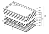
- FIG. 1 is an exploded perspective view showing a schematic configuration of the entire liquid crystal display device according to the embodiment.
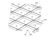
- FIG. 2 is a partially enlarged view of the reflection sheet in the embodiment.
- FIG. 3 is a schematic diagram illustrating a positional relationship among the light source, the plurality of partition walls, and the luminance uniform plate in the embodiment.
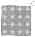
- FIG. 4 is a plan view of an example of a uniform luminance plate according to the embodiment.
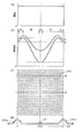
- FIG. 5 is a diagram illustrating an example of the unit pattern of the uniform luminance plate and the light transmittance within the unit pattern in the embodiment.
- FIG. 6 is a partially enlarged view of a reflective sheet in a modification of the embodiment.
- FIG. 1 is an exploded perspective view showing a schematic configuration of the entire liquid crystal display device according to the embodiment.
- the liquid crystal display device 10 includes a liquid crystal panel 11, a bezel 12, a backlight device 20 on a rectangular shape that is disposed on the back side of the liquid crystal panel 11 and has a size corresponding to the liquid crystal panel 11. Consists of.
- the liquid crystal panel 11 is a transmissive liquid crystal panel having a rectangular flat plate shape, and displays an image by transmitting or blocking light emitted from the backlight device 20 located on the back surface thereof.
- the bezel 12 is a casing on the front surface of the liquid crystal display device 10, and surrounds the liquid crystal panel 11 to protect the peripheral portion thereof.
- a plastic resin is mainly used from the viewpoints of design and lightness in the product.
- the backlight device 20 includes a plurality of printed boards 27 on which a plurality of light sources 21 are mounted, a chassis 22 that houses the plurality of printed boards 27, an optical unit 26 that is disposed between the liquid crystal panel 11 and the light sources 21, and a diffusion plate 25, a uniform luminance plate 24, and a reflection sheet 23.
- the printed circuit board 27 is supplied with electric power from a power source (not shown), and supplies this electric power to each light source 21 as driving electric power.
- the printed circuit board 27 in the present disclosure has a substantially rectangular shape, and six light sources 21 are mounted in a row along the longitudinal direction. According to FIG. 1, the plurality of printed circuit boards 27 are arranged in 7 rows ⁇ 2 columns in the chassis 22. As a result of this arrangement of the printed circuit board 27, the plurality of light sources 21 are arranged in a matrix. Note that the shape, size, number, and arrangement of the printed circuit boards 27 and the number of light sources 21 mounted on each printed circuit board 27 are not the gist of the present disclosure, and do not limit the present invention.
- the plurality of light sources 21 may be configured by using a plurality of types of light sources that emit monochromatic light such as red light, blue light, and green light, or may be configured only by light sources that emit white light. Also good. For example, an LED is used as such a light source 21.
- the chassis 22 is also a casing on the back surface of the liquid crystal display device 10.
- the chassis 22 is made of, for example, a plastic, a metal having a high-radiation ceramic sheet attached to the front or back, a metal anodized such as black, or a metal coated with carbon black.
- a metal anodized such as black
- a metal coated with carbon black As these metals, for example, alloys mainly composed of aluminum or iron are used.
- the reflection sheet 23 is a component made of a substantially flat resin, and its main surface is, for example, a mirror surface or white, and efficiently reflects light incident on the main surface.
- this main surface is also referred to as a reflective surface.
- This reflection surface is partitioned into a plurality of reflection regions 232 arranged in a matrix by a plurality of ridge-like partition walls 231 arranged in a lattice pattern.
- the saddle shape here means that the shape of the cross section perpendicular to the extending direction of the partition wall 231 has a width toward the top (in a direction opposite to the direction in which the chassis 22 is located) like a substantially triangular shape or a substantially trapezoidal shape. A shape that narrows.
- the vertical and horizontal pitches of the reflection areas 232 are the same as the vertical and horizontal pitches of the light sources 21 on the chassis 22.
- each light source 21 is arranged every 50 mm.
- Each reflection region 232 includes an opening 233 at substantially the center.
- FIG. 2 is a partially enlarged view of the state in which the reflection sheet 23 is superimposed on the chassis 22 in the present embodiment.
- the opening 233 is provided so that the light source 21 exits from the surface of the reflection sheet 23 in this state. Therefore, in the assembled liquid crystal display device 10, the light source 21 is disposed in each of the reflection regions 232.
- the reflection sheet 23 reflects the light emitted from each light source 21 in the direction of the luminance uniform plate 24.
- Such a reflection sheet 23 is produced by, for example, forming unevenness on a resin flat plate by vacuum forming.
- the bowl-shaped partition 231 has a height of 4.5 mm and is provided at a pitch of 50 mm. Further, processing such as drilling is performed as necessary.
- the luminance uniform plate 24 is a plate-shaped part made of a highly reflective and translucent resin (for example, polyethylene terephthalate).
- the uniform luminance plate 24 is arranged so that one main surface (hereinafter also referred to as a first surface) of the liquid crystal display device 10 in an assembled state faces the reflective surface of the reflective sheet 23 at a distance from the first surface.
- the light emitted from the light source 21 and the light reflected from the reflection sheet 23 are received. Then, the emitted light and the reflected light are transmitted, and emitted from the second surface, which is the main surface opposite to the first surface, as light with increased uniformity of luminance.
- the configuration of the luminance uniform plate 24 for emitting the light with enhanced luminance uniformity will be described later.
- Such a uniform brightness plate 24 is formed by molding the above-mentioned resin as a material, for example, by pressing.
- the diffuser plate 25 is a plate-like component having a refractive index higher than that of air, and is mainly made of, for example, an acrylic resin such as polymethyl methacrylate, polycarbonate, or the like, and a material containing fine particles dispersed throughout. Become. In the assembled liquid crystal display device 10, the diffusion plate 25 is positioned on the second surface side of the uniform luminance plate 24, and the light incident from the surface of the main surface facing the second surface of the uniform luminance plate 24 is the particle. And is emitted from the main surface opposite to the main surface.
- a diffusion plate 25 can be produced by, for example, injection molding the above-mentioned material.
- the optical unit 26 is located between the liquid crystal panel 11 and the diffusion plate 25 in the assembled liquid crystal display device 10 and faces the surface of the diffusion plate 25 from which light is emitted.
- the optical unit 26 has a size corresponding to the liquid crystal panel 11 and includes an optical sheet stack for further diffusing and collecting the light emitted from the diffusion plate 25.
- the optical sheet laminate includes, for example, a prism sheet that condenses incident light from the diffusion plate 25 toward a certain direction, a diffusion sheet that further diffuses incident light from the diffusion plate 25, and the diffusion plate 25.
- a polarizing sheet or the like that transmits light having a specific polarization plane corresponding to the polarization axis of the liquid crystal panel 11 is used.
- the brightness of the light emitted from the optical unit 26 is made uniform from the time of incidence, and the brightness uniformity of the backlight device 20 as the surface light source of the liquid crystal display device 10 is further increased.
- light derived from the light source 21 incident on the luminance uniform plate 24 from the first surface can be divided into the following three types having different paths.
- One is direct light from the light source 21.
- the other is reflected light that is reflected by the reflecting sheet 23 and is incident only once after being emitted from the light source 21.
- Another one is reflected light that is emitted from the light source 21 and then reflected m times on the reflection sheet 23 and n times on the luminance uniform plate 24 (m is an integer of 1 or more, and n is an integer of 1 or more).
- the sum of m and n is an integer of 2 or more).
- the incident light to the luminance uniform plate 24 composed of these three types of light is added in the region facing each reflection region 232, and the light is increased in luminance uniformity through the luminance uniform plate.
- the luminance uniform plate 24 increases the luminance uniformity
- FIG. 3 is a schematic diagram showing the positional relationship between the light source 21, the plurality of partition walls 231, and the luminance uniform plate 24 on one reflection region 232 of the backlight device 20 according to the present embodiment.
- (A) is sectional drawing of the reflective sheet 23 and the luminance uniform board 24,
- (b) is the top view which looked at the reflective sheet 23 from the luminance uniform board 24 side.
- a broken line is a boundary of the reflection region 232 surrounded by four partition walls 231 (here, these are distinguished, and reference numerals of the partition walls 231a to 231d are attached to indicate correspondence between (a) and (b)), And the boundary of the area
- Dotted arrows L1 to L6 indicate examples of light paths toward the first surface.
- the outline of the cross section of the partition wall 231 is a straight line, but the cross section of the partition wall 231 may be a straight line, a curve, or both.
- the partition wall 231 is drawn as a mountain-folded portion of the reflection sheet 23, but the partition wall 231 may be a hook-like protrusion on the reflection surface side of the reflection sheet 23, and the structure is not limited to the illustrated one.
- the incident light to the uniform luminance plate 24 attenuates according to the moving distance after emission from the light source 21, more specifically, in inverse proportion to the square of the moving distance.
- the direct light is attenuated according to the distance of the path from the light source 21 until reaching the first surface of the luminance uniform plate 24.
- the lengths of arrows L1 and L2 in (a) in this figure and arrows L5 and L6 in (b) indicate the travel distance of direct light from the light source 21, and incident light correlates with this travel distance. It is decaying. That is, the incident light that is further from the light source 21 and enters the luminance uniform plate 24 is more attenuated.
- the reflection sheet 23 includes the partition wall 231 protruding toward the luminance uniform plate 24 side, and therefore the distance between the reflection surface and the first surface varies depending on the location (for example, arrows L3 and L4). ). Therefore, similarly to the direct light, the degree of attenuation of the reflected light varies depending on the incident location.
- the intensity of the reflected light incident on the uniform luminance plate 24 correlates not only with the moving distance as described above but also with the number of times reflected by the reflective sheet 23 and the uniform luminance plate 24 before incidence. More precisely, the reflected light is weakened in correlation with the m-th power of the reflectance of the reflection sheet 23 and the n-th power of the luminance uniform plate 24 (m and n are as described above) in addition to the moving distance.
- the light emitted from the light source 21 has some attenuation factors before entering the luminance uniform plate 24, and the degree of attenuation is uniform luminance facing one reflection region 232.
- the degree of attenuation is uniform luminance facing one reflection region 232.
- the region facing the partition wall 231 and the other region arrows L3 and L4.
- the distance from the reflecting surface is also different in the region facing the partition wall 231.
- the reflected light that is reflected at the highest part of the partition wall 231 hereinafter also referred to as the top of the partition wall 231 and enters the region facing this part has the smallest attenuation rate due to the moving distance.
- the intensity of the incident light composed of such direct light and reflected light in the entire area of the uniform luminance plate 24 facing one reflection area 232 is, for example, the strongest in the area facing the light source 21 and as the distance from the light source 21 increases.
- the distribution is such that the distance from the light source 21 increases, that is, the region becomes stronger as it approaches the top.
- the incident light in the region where the luminance uniform plate 24 faces the top of the partition wall 231 is weaker than the region facing the light source 21.
- the transmittance with respect to the incident light (hereinafter also simply referred to as light transmittance) in each region facing the reflection region 232 of the luminance uniform plate 24 is changed in a predetermined pattern to change the inside of the region.
- the uniformity of the brightness of the light emitted from the second surface is increased.
- the predetermined pattern is that the distribution of light transmittance of the luminance uniform plate 24 in the region facing each reflection region 232 of the luminance uniform plate 24 is the intensity of incident light to the luminance uniform plate 24. It has a negative correlation.
- the product of the intensity of incident light and the light transmittance at each location is brought close to a constant, and the uniformity of the brightness of the light emitted from the brightness uniform plate 24 is increased.
- the contrast between the bright part and the dark part in the screen corresponding to the image displayed on the entire screen is increased.
- the configuration of the uniform brightness plate 24 that realizes the predetermined pattern will be described by taking as an example the case where the intensity of incident light on the uniform brightness plate 24 exhibits the above-described distribution.
- FIG. 4 is a plan view (part) of an example of the uniform luminance plate 24 in the present embodiment.
- a large number of circles seen in this figure indicate through-holes 241 penetrating between the first surface and the second surface of the luminance uniform plate 24. That is, the uniform luminance plate 24 shown in the figure has a plurality of through holes 241 penetrating between the first surface and the second surface.
- the through hole 241 in this example has variations in size (opening area of each through hole). These through holes 241 having different sizes are arranged so as to form one pattern in the entire region facing one reflection region 232 of the luminance uniform plate 24, and this pattern is repeated vertically and horizontally over the entire luminance uniform plate 24. It is.
- the plurality of through holes 241 arranged so as to form such a single pattern are, for example, a plurality of protrusions that penetrate the flat plate of the resin material in one step of press processing for forming the above-described luminance uniform plate 24. It is provided using the type
- the predetermined pattern of the light transmittance described above is realized by a pattern (hereinafter referred to as a unit pattern) over the entire region facing this one reflection region 232.
- this unit pattern will be described.
- FIG. 5 is a diagram showing an example of the unit pattern of the uniform luminance plate 24 and the light transmittance within the unit pattern in the present embodiment.
- This unit pattern is shown in (c) of this figure, and (b) shows the light transmittance on line A and the light transmittance on line B of the luminance uniform plate 24 having this unit pattern.
- It is a graph.
- (D) of this figure is sectional drawing which shows the cut surface obtained by cut
- (A) is a graph which shows the intensity
- the horizontal axes of the graphs of (a) and (b) correspond to the horizontal position of the unit pattern shown in (c) and the horizontal position of the reflection sheet 23 shown in (d).
- the light transmittance used in the description of the unit pattern means the light transmittance per unit area.
- the light transmittance indicated by this graph is the same as that of the incident light on the first surface passing through the through hole 241 and the light emitted from the opening on the second surface side and the resin within the unit area. It is a total ratio with the light which appeared on the 2nd surface side.
- region which has a unit area in this indication shall not be settled in opening of arbitrary through-holes 241.
- the material of the uniform brightness plate 24 has translucency, but is not transparent. More specifically, the luminance uniform plate 24 is a resinous white plate having a through hole 241. Therefore, the uniform luminance plate 24 transmits light to some extent even in an arbitrary region that does not include the through hole 241.
- the range in which the light transmittance near the center of the graph corresponding to the line A is constant corresponds to a region near the center in the diagram (c) where there is no through hole 241. The reason why the light transmittance is not zero in this range is due to the translucency of the material of the uniform luminance plate 24 itself.
- the through holes 241 allow light to pass from the first surface side to the second surface side of the luminance uniform plate 24 at a higher rate (substantially 100%) than the resin that is the material of the luminance uniform plate 24. Therefore, in the region of the unit area, the light transmittance of this region increases as the opening area of the through hole 241 increases. In other words, the opening area of the through hole 241 per unit area of the luminance uniform plate 24 and the light transmittance have a positive correlation. Then, by changing the opening area per unit area (hereinafter also referred to as the aperture ratio) depending on the location, the light transmittance in the region of the luminance uniform plate 24 facing one reflection region 232 is changed.
- the aperture ratio the opening area per unit area
- the light transmittance is increased by increasing the aperture ratio, and the light transmittance is decreased by decreasing the aperture ratio.
- the pitch between the through holes 241 is uniform in the region where the through holes 241 exist, and the aperture ratio is changed by changing the size of each through hole 241. As a result, the light transmittance is changed.
- the intensity of the incident light in the region of the luminance uniform plate 24 facing one reflection region 232 is the strongest in the region facing the light source 21 as described above, and decreases as the distance from the light source 21 increases. In the region facing the partition wall 231, it becomes stronger as it approaches the top. That is, in the region of the brightness uniform plate 24 that does not face the partition wall 231, the intensity of incident light and the distance from the light source 21 have a negative correlation.
- the product of the intensity of incident light and the light transmittance in this region approaches a constant between the distance from the light source 21 and the light transmittance of the uniform luminance plate 24. Have a positive correlation.
- the luminance of the emitted light from the second surface of the uniform luminance plate 24 in this region is brought close to a constant state regardless of the distance from the light source 21 as shown in FIG. Can do.
- the aperture area per unit area of the luminance uniform plate 24 and the distance from the light source 21 have a positive correlation.
- a hole 241 is provided in the luminance uniform plate 24. This region substantially corresponds to the range indicated by III and IV in FIG.
- FIG. 5B there is a difference between the light transmittance on the line A and the light transmittance on the line B even at the same left and right positions. This reflects the difference in the degree of attenuation.
- the through-hole 241 is not provided as shown in the figure in the region facing the light source 21 and in the vicinity thereof. This region substantially corresponds to the range indicated by IV in FIG.
- the region where the through-holes 241 are not provided as described above is appropriately determined according to, for example, the light distribution of the light source 21 and the degree of diffusion of incident light (scattering in the luminance uniform plate 24) by the luminance uniform plate 24.
- the intensity of incident light and the distance from the partition wall 231 have a negative correlation.
- the backlight device 20 in the present embodiment has a relationship between the intensity of incident light and the light transmittance in this area. A positive correlation is given so that the product approaches a constant value. As a result, the brightness of the emitted light from the second surface of the uniform brightness plate 24 in this region can be brought close to a constant state regardless of the distance from the top as shown in FIG. it can.
- the opening area per unit area of the luminance uniform plate 24 and the distance from the top of the partition 231 have a positive correlation in the region facing the partition 231 of the luminance uniform plate 24.
- a through-hole 241 is provided in the luminance uniform plate 24 so that there is a region. This region substantially corresponds to the range indicated by I and II in FIG.
- the distribution of the light transmittance of the luminance uniform plate 24 provided with the through-holes 241 as described above will be described with reference to the entire region of the luminance uniform plate 24 facing one reflection region 232.
- a region having a higher light transmittance than any of these regions is between the region facing the light source 21 and the region facing the top of the partition wall 231. If this region is shown more specifically, it can be said that the luminance uniform plate 24 is in the vicinity of the boundary between the region facing the partition wall 231 and the other region. In FIG. 5B, this region is a region near the peak of each curve, which is near the boundary between the range indicated by II and the range indicated by III. Further, the light transmittance has a minimum value in a region facing the light source 21.
- This region is included in the range indicated by IV in FIG.
- the maximum value is found between the region facing the light source 21 and the region facing the top of the partition wall 231.
- the opening area of one through-hole 241 inside the region of the luminance uniform plate 24 not facing the partition wall 231 and in the vicinity of the corner is the highest (that is, the light transmittance is high). ).
- the boundaries of these areas are not strictly determined based on these positional relationships. It may vary to some extent due to light scattering by the reflection surface of the reflection sheet 23, diffusion of incident light by the luminance uniform plate 24 (scattering in the luminance uniform plate 24), and the like. For this reason, in the design of the uniform luminance plate 24, it is necessary to appropriately adjust the light transmittance distribution in consideration of the influence of these variable factors.
- the through holes 241 are arranged at an equal pitch, and the aperture ratio is changed by changing the size of each through hole 241, but the luminance uniform plate 24 in the present invention.
- the configuration is not limited to this. Any configuration may be used as long as the light transmittance distribution in the unit pattern of the luminance uniform plate 24 as described above can be obtained.
- the opening area of the plurality of through holes 241 may be the same, and the opening ratio may be changed by changing the number of through holes 241 per unit area, that is, the density of the through holes 241.
- the opening area of each through-hole 241 in a region not facing the partition wall 231 has a positive correlation with the distance from the light source 21, but the opening for each through-hole 241. If there is a variation in area, this correlation may be absent. In other words, a positive correlation may be established between the distance from the light source 21 and the aperture ratio, and the aperture ratio may be satisfied by the plurality of through holes 241. For example, depending on the location, the through hole 241 having a larger opening area may be provided so as to surround the through hole 241 having a smaller opening area. Alternatively, the through hole 241 having a smaller opening area may be provided so as to surround the through hole 241 having a larger opening area.
- the arrangement of the through holes 241 is not limited to the example of the unit pattern shown in FIG.
- FIG. Moreover, you may arrange
- the shape of the through hole 241 is not limited to a circle as shown in FIGS. Moreover, the shape of all the through-holes 241 may not be congruent or similar. That is, there may be variations in the shape of the through hole 241.
- a negative correlation may be given between the light transmittance of the uniform luminance plate 24 and the intensity of light received by the uniform luminance plate 24 on the first surface.
- the light transmittance of the luminance uniform plate 24 may be changed by applying a light shielding agent such as a paint having a light shielding property to the luminance uniform plate 24 in a predetermined pattern.
- the light transmittance of the uniform luminance plate 24 may be changed by applying the light shielding agent while changing the application area per unit area of the uniform luminance plate 24. In this case, for example, it is realized by applying paint so as to draw dots having different areas depending on the location, or changing the density of dots drawn by the paint.
- the concentration of the paint may be changed depending on the place, or paints having different light transmittances may be used.
- a non-through hole may be used instead of the through hole 241. That is, the light transmittance of the uniform luminance plate 24 may be changed by changing the average thickness per unit area of the uniform luminance plate 24. The configuration not including these through holes is also applied so that the light transmittance distribution of the uniform luminance plate 24 has the same characteristics as described above.
- the through hole 241 and the above-described light shielding agent or non-through hole may be used in combination.
- FIG. 6 is a partially enlarged view of a reflective sheet 23a according to a modification of the above embodiment.
- the reflective sheet 23 a is different from the reflective sheet 23 in that the reflective sheet 23 a has support pillars 234 that protrude toward the uniform brightness plate 24 on the partition wall 231 that projects in the direction in which the uniform brightness plate 24 exists.
- the support column 234 supports the luminance uniform plate 24 in a state where the tip is inserted into the hole of the luminance uniform plate 24.
- the uniform brightness plate 24 is prevented from being bent by its own weight.
- the larger luminance uniform plate 24 is used in accordance with the display surface.
- an increase in the size of the uniform luminance plate 24 causes a deflection due to its own weight. If the thickness of the luminance uniform plate 24 is increased in order not to cause this deflection, a decrease in the light transmittance due to the increase in the thickness may result in insufficient luminance of the emitted light to the diffusion plate, or to avoid this insufficient luminance.
- the uniform luminance plate 24 There is an influence such as a change in specifications of the uniform luminance plate 24 or other components. As described above, it is not preferable to increase the thickness of the uniform luminance plate 24 in order to prevent the deflection. Further, even when the liquid crystal display device 10 is relatively small, the uniform brightness plate 24 is easily bent by providing the plurality of through holes 241 as in the present disclosure. The bent uniform brightness plate 24 cannot obtain an appropriate positional relationship between the light source 21 and the partition wall 231 in each reflection region 232 as described above, and therefore cannot increase the brightness uniformity.
- the support pillar 234 described above may be provided.
- positioning of the support pillar 234 shown by FIG. 6 are examples, and are not limited to this.
- only one of the support pillars 234 that protrude from the center of the reflection sheet 23 a and fit into a hole in the center of the luminance uniform plate 24 may be provided.
- it may be arranged at a position where the partition walls 231 arranged in a lattice shape intersect, or may be arranged at other positions as shown in the figure.
- the hole of the luminance uniform plate 24 into which the tip of the support column 234 is inserted is provided separately from the hole for giving the luminance uniform plate 24 a predetermined light transmittance distribution pattern.
- a support column 234 is formed by processing a highly reflective material such as polycarbonate by injection molding or the like. The material may be the same as or different from that of the reflection sheet 23a. Moreover, it may be molded integrally with the reflection sheet 23a, or may be prepared separately from the reflection sheet 23a and attached to the reflection sheet 23a.
- a support column 234 affects the intensity of light reaching the first surface of the luminance uniform plate 24 due to a difference in material from the reflection sheet 23 a or a difference in shape from the surrounding partition wall 231. Under this influence, the light reaching the first surface around the support pillar 234 may become stronger or weaker. That is, it causes unevenness in the intensity of light incident on the luminance uniform plate 24.
- the uniform brightness plate 24 may have a light transmittance distribution pattern that suppresses unevenness of light intensity caused by the support pillars 234.
- the luminance uniform plate 24 supported by the support pillar 234 is a positive region between the opening area per unit area and the distance from the top of the partition wall around the support pillar 234 in the region facing the plurality of partition walls.
- Each light source 21 is controlled to be turned on or off independently.
- the light emitted from the light source 21 becomes direct light, and the light reflected by the reflection sheet 23 after being reflected by the reflection sheet 23 or the luminance uniform plate 24 is reflected light. Is incident on the uniform luminance plate 24.
- interference of light emitted from the light source 21 in each reflection region 232 to the surrounding reflection region 232 is caused by the hook-shaped partition wall 231 provided around each light source 21 and projecting toward the luminance uniform plate 24. Is suppressed.
- the brightness uniform plate 24 emits light with a higher degree of brightness uniformity.
- the light emitted from the uniform luminance plate 24 enters the diffusion plate 25.
- the incident light to the uniform brightness plate 24 is attenuated according to the moving distance from the light source 21 and the number of reflections, and the intensity varies depending on the location.
- the light transmittance distribution of the uniform luminance plate 24 is negatively correlated with such unevenness in the intensity of incident light.
- the light transmittance per unit area is changed depending on the place. More specifically, large through holes 241 are provided or the through holes 241 are provided at high density so that the aperture ratio is relatively large in a region where incident light is relatively strong. This is, for example, a region that does not face the partition wall 231 and that is away from the light source 21.
- the through hole 241 is provided so that the aperture ratio is relatively small at a place where the distance from the partition wall 231 is relatively short, and the aperture ratio is relatively large at a place where this distance is long.
- the through hole 241 is not provided in the region that faces the light source 21 and receives strong direct light. Thereby, the difference in intensity depending on the location of the incident light on the luminance uniform plate 24 is absorbed, and the uniformity of the luminance of the outgoing light to the diffusion plate 25 can be increased.
- the intensity of light incident on the luminance uniform plate 24 is uneven due to the light reflection characteristics of the support column 234.
- the unevenness of the intensity of light is also absorbed by changing the light transmittance per unit area of the luminance uniform plate 24 around the support column 234, for example, around the support column 234, and thereby the luminance uniform plate 24.
- the uniformity of the emitted light can be increased.
- the diffusion plate 25 diffuses the light with the increased brightness uniformity in this way, and emits the light with a higher uniformity.
- the light emitted from the diffusing plate 25 is further diffused and condensed by the optical unit 26 and irradiated onto the liquid crystal panel 11.
- the backlight device is disposed in each of the reflection sheet having a reflection surface partitioned into a plurality of reflection regions by a plurality of bowl-shaped partition walls and the plurality of reflection regions of the reflection surface.
- a plurality of light sources to be transmitted, and light emitted from the plurality of light sources received by the first surface facing the reflection surface and reflected light from the reflection sheet are transmitted, and the second light beam is opposite to the first surface.
- a backlight device comprising a uniform luminance plate that emits from a surface and a diffuser plate that diffuses and emits light emitted from the second surface, wherein the uniform luminance plate is a region facing the light source; Between the area
- the luminance uniform plate 24 has a light transmittance distribution having a negative correlation with the intensity of incident light that varies depending on the location, and increases the uniformity of the luminance of the emitted light.
- the uniform luminance plate has a plurality of through holes penetrating between the first surface and the second surface, and the opening area of the through hole per unit area of the uniform luminance plate and the light
- the transmittance may have a positive correlation.
- the light transmittance increases in a region including the opening. Further, by changing the opening area per unit area, the light transmittance of the region including the opening can be changed. Thereby, the light transmittance distribution as described above can be given to the luminance uniform plate 24. That is, the uniformity of the brightness of light emitted from the brightness uniform plate 24 to the diffusion plate 25 can be increased.
- the opening area per unit area and the distance from the top of the partition may have a positive correlation.
- the light transmittance of the uniform luminance plate 24 is suppressed in a region that receives reflected light with a small attenuation due to distance among light reflected by the reflection sheet 23, and is increased in a region that receives reflected light with a large attenuation due to distance. Can do.
- the uniformity of the luminance of the light emitted from the luminance uniform plate 24 to the diffusion plate 25 can be increased.
- the opening area per unit area and the distance from the light source may have a positive correlation. That is, the light transmittance of the uniform luminance plate 24 may be suppressed in a region that receives direct light with a small attenuation due to distance among light emitted from the light source 21, and may be increased in a region that receives direct light with a large attenuation due to distance. it can. Thereby, the uniformity of the luminance of the light emitted from the luminance uniform plate 24 to the diffusion plate 25 can be increased.
- the light transmittance per unit area in the region of the luminance uniform plate facing the reflection region takes a minimum value in the region facing the light source, the region facing the light source, and the top of the partition wall A maximum value may be taken between the regions facing each other. That is, the light transmittance of the uniform luminance plate 24 is the lowest in the region receiving the strongest light in the region facing the reflection region 232. Further, in this region, the light transmittance is highest in a region that receives direct light attenuated compared to the light received by the region receiving the strongest light and also has a large attenuation of the reflected light received from the reflection sheet 23. Thereby, the uniformity of the luminance of the light emitted from the luminance uniform plate 24 to the diffusion plate 25 can be increased.
- the reflection sheet further includes a support column that protrudes toward the luminance uniform plate on the plurality of partition walls and supports the luminance uniform plate, and the reflection sheet includes a support column in a region facing the plurality of partition walls.
- the opening area per unit area and the distance from the top of the partition do not have a positive correlation.
- a liquid crystal display device includes a liquid crystal panel, and any one of the backlight devices disposed on the back side of the liquid crystal panel and corresponding to the liquid crystal panel. This provides a liquid crystal display device that provides high-contrast expression over the entire screen by area control and that has a high degree of luminance uniformity within the area of the unit of luminance control.
- the shape and size of each component and the ratio of sizes between components are examples, and the present invention is not limited to this.
- the slope of the partition wall 231 may be gentler or steep.
- the slope of the partition wall 231 may vary depending on the location in the reflection region 232.
- the slope of the partition wall 231 is gentle at the four corners of the reflection region 232 in plan view, and may be closer to the light source 21 than shown in FIGS.
- the correlation between the aperture ratio of the uniform luminance plate 24 and the distance from the top of the partition wall 231 or the light source 21 is as described above.
- the method of creating each component is not limited to the one described in the embodiment.
- the uniform brightness plate 24 may be formed by injection molding a resin as a material.
- various processing methods applicable as necessary may be used.
- the through-hole 241 of the uniform luminance plate 24 may be provided by punching in press working, or may be provided by drilling using a drill, a laser, or the like.
- the present disclosure can be applied to a backlight device and a liquid crystal display device including the backlight device in general.
Landscapes
- Physics & Mathematics (AREA)
- Nonlinear Science (AREA)
- Mathematical Physics (AREA)
- Chemical & Material Sciences (AREA)
- Crystallography & Structural Chemistry (AREA)
- General Physics & Mathematics (AREA)
- Optics & Photonics (AREA)
- Planar Illumination Modules (AREA)
- Liquid Crystal (AREA)
Abstract
Le dispositif de rétroéclairage (20) de l'invention comprend : une feuille réfléchissante (23) comprenant une surface réfléchissante divisée en une pluralité de régions réfléchissantes (232) par une pluralité de parois de séparation en forme de nervure (231) ; une pluralité de sources lumineuses (21) qui sont disposées respectivement dans la pluralité de régions réfléchissantes (232) ; une plaque à luminance uniforme (24) à travers laquelle une lumière faisant incidence sur sa première surface, opposée à la surface réfléchissante, est autorisée à être émise, et qui émet la lumière depuis sa deuxième surface ; et une plaque de diffusion (25) qui diffuse et émet la lumière qui a été émise par la deuxième surface et qui est entrée dans la plaque de diffusion (25), la plaque à luminance uniforme (24) comprenant, entre une région opposée à chacune des sources lumineuses (21) et une région opposée à la section supérieure d'une des parois de séparation (231) qui correspond, une région ayant une transmittance de lumière plus élevée par unité de surface que la région opposée à la source lumineuse (21) ou la région opposée à la section supérieure de la paroi de séparation (231).
Priority Applications (3)
| Application Number | Priority Date | Filing Date | Title |
|---|---|---|---|
| EP16877918.9A EP3396233B1 (fr) | 2015-12-25 | 2016-08-24 | Dispositif de rétroéclairage et appareil d'affichage à cristaux liquides |
| JP2017557674A JP6785432B2 (ja) | 2015-12-25 | 2016-08-24 | バックライト装置及び液晶表示装置 |
| US15/962,828 US10466536B2 (en) | 2015-12-25 | 2018-04-25 | Backlight device and liquid crystal display apparatus |
Applications Claiming Priority (2)
| Application Number | Priority Date | Filing Date | Title |
|---|---|---|---|
| JP2015255447 | 2015-12-25 | ||
| JP2015-255447 | 2015-12-25 |
Related Child Applications (1)
| Application Number | Title | Priority Date | Filing Date |
|---|---|---|---|
| US15/962,828 Continuation US10466536B2 (en) | 2015-12-25 | 2018-04-25 | Backlight device and liquid crystal display apparatus |
Publications (1)
| Publication Number | Publication Date |
|---|---|
| WO2017110013A1 true WO2017110013A1 (fr) | 2017-06-29 |
Family
ID=59091124
Family Applications (1)
| Application Number | Title | Priority Date | Filing Date |
|---|---|---|---|
| PCT/JP2016/003846 Ceased WO2017110013A1 (fr) | 2015-12-25 | 2016-08-24 | Dispositif de rétroéclairage et appareil d'affichage à cristaux liquides |
Country Status (4)
| Country | Link |
|---|---|
| US (1) | US10466536B2 (fr) |
| EP (1) | EP3396233B1 (fr) |
| JP (1) | JP6785432B2 (fr) |
| WO (1) | WO2017110013A1 (fr) |
Cited By (2)
| Publication number | Priority date | Publication date | Assignee | Title |
|---|---|---|---|---|
| WO2025071021A1 (fr) * | 2023-09-27 | 2025-04-03 | 삼성전자주식회사 | Appareil d'affichage |
| US12493213B2 (en) | 2023-09-27 | 2025-12-09 | Samsung Electronics Co., Ltd. | Display apparatus |
Families Citing this family (6)
| Publication number | Priority date | Publication date | Assignee | Title |
|---|---|---|---|---|
| US10969628B1 (en) * | 2017-09-28 | 2021-04-06 | Apple Inc. | Backlight units with support posts and cavity height monitoring |
| JP7275428B2 (ja) * | 2019-03-08 | 2023-05-18 | 船井電機・ホールディングス株式会社 | バックライト装置及び液晶表示装置 |
| CN110441957B (zh) * | 2019-06-10 | 2021-06-11 | 惠科股份有限公司 | 一种显示模组和显示装置 |
| KR102747582B1 (ko) * | 2020-03-24 | 2025-01-02 | 삼성디스플레이 주식회사 | 광원 부재, 이를 포함한 표시 장치, 및 광원 부재의 제조 방법 |
| KR102852971B1 (ko) * | 2020-07-20 | 2025-09-01 | 삼성전자주식회사 | 백라이트 유닛 및 이를 포함하는 디스플레이 장치 |
| JP2023005241A (ja) * | 2021-06-28 | 2023-01-18 | 船井電機株式会社 | 表示装置およびバックライト装置 |
Citations (2)
| Publication number | Priority date | Publication date | Assignee | Title |
|---|---|---|---|---|
| JP2010272245A (ja) * | 2009-05-19 | 2010-12-02 | Toshiba Corp | バックライトユニットおよびこれを備えた液晶表示装置 |
| JP2011151002A (ja) | 2009-11-16 | 2011-08-04 | Opt Design:Kk | 面光源ユニット、面照明装置及び液晶表示装置 |
Family Cites Families (3)
| Publication number | Priority date | Publication date | Assignee | Title |
|---|---|---|---|---|
| JP2010135204A (ja) * | 2008-12-05 | 2010-06-17 | Citizen Electronics Co Ltd | 面状光源及び液晶表示装置 |
| US9632357B2 (en) * | 2012-07-17 | 2017-04-25 | Lg Electronics Inc. | Display device |
| EP3273297B1 (fr) * | 2016-07-20 | 2021-05-26 | Nichia Corporation | Dispositif électroluminescent |
-
2016
- 2016-08-24 JP JP2017557674A patent/JP6785432B2/ja not_active Expired - Fee Related
- 2016-08-24 WO PCT/JP2016/003846 patent/WO2017110013A1/fr not_active Ceased
- 2016-08-24 EP EP16877918.9A patent/EP3396233B1/fr active Active
-
2018
- 2018-04-25 US US15/962,828 patent/US10466536B2/en not_active Expired - Fee Related
Patent Citations (2)
| Publication number | Priority date | Publication date | Assignee | Title |
|---|---|---|---|---|
| JP2010272245A (ja) * | 2009-05-19 | 2010-12-02 | Toshiba Corp | バックライトユニットおよびこれを備えた液晶表示装置 |
| JP2011151002A (ja) | 2009-11-16 | 2011-08-04 | Opt Design:Kk | 面光源ユニット、面照明装置及び液晶表示装置 |
Cited By (2)
| Publication number | Priority date | Publication date | Assignee | Title |
|---|---|---|---|---|
| WO2025071021A1 (fr) * | 2023-09-27 | 2025-04-03 | 삼성전자주식회사 | Appareil d'affichage |
| US12493213B2 (en) | 2023-09-27 | 2025-12-09 | Samsung Electronics Co., Ltd. | Display apparatus |
Also Published As
| Publication number | Publication date |
|---|---|
| EP3396233B1 (fr) | 2021-04-14 |
| JPWO2017110013A1 (ja) | 2018-10-11 |
| JP6785432B2 (ja) | 2020-11-18 |
| EP3396233A4 (fr) | 2018-12-05 |
| US10466536B2 (en) | 2019-11-05 |
| US20180239197A1 (en) | 2018-08-23 |
| EP3396233A1 (fr) | 2018-10-31 |
Similar Documents
| Publication | Publication Date | Title |
|---|---|---|
| JP6785432B2 (ja) | バックライト装置及び液晶表示装置 | |
| JP6695035B2 (ja) | バックライト装置および液晶表示装置 | |
| JP6315179B2 (ja) | 面発光装置及び液晶表示装置 | |
| US20120013811A1 (en) | Lighting device, display device and television receiver | |
| WO2017002308A1 (fr) | Dispositif de rétroéclairage et dispositif d'affichage à cristaux liquides | |
| US8567977B2 (en) | Illumination system and display device | |
| US20120256974A1 (en) | Light source device, display, and electronic unit | |
| US20150292708A1 (en) | Optical Element and Backlight Unit Including the Same | |
| KR20100126984A (ko) | 백라이트 유닛 및 그를 구비한 액정표시장치 | |
| WO2017154050A1 (fr) | Dispositif de rétroéclairage et dispositif d'affichage à cristaux liquides | |
| JP6580161B2 (ja) | 表示装置 | |
| JP6990279B2 (ja) | 光源装置、照明装置、及び表示装置 | |
| KR20180064126A (ko) | 디스플레이 장치 | |
| WO2013088556A1 (fr) | Lentille optique, module optique, ensemble de rétroéclairage et dispositif d'affichage | |
| KR102425442B1 (ko) | 표시 장치 | |
| JP2009258317A (ja) | 表示装置 | |
| US20190121012A1 (en) | Display apparatus with a diffusion plate support member | |
| JP6924307B2 (ja) | 照明装置及び表示装置 | |
| TWI722799B (zh) | 面光源裝置及液晶顯示裝置 | |
| US9477114B2 (en) | Direct type backlight module and liquid crystal display device having same | |
| WO2013064369A1 (fr) | Dispositif d'éclairage de surface | |
| WO2017104081A1 (fr) | Dispositif d'affichage | |
| JP2007157520A (ja) | 側面入射光源混合式バックライト | |
| KR20070113577A (ko) | 백라이트 어셈블리 | |
| WO2013080344A1 (fr) | Dispositif de rétroéclairage et dispositif d'affichage à cristaux liquides l'utilisant |
Legal Events
| Date | Code | Title | Description |
|---|---|---|---|
| 121 | Ep: the epo has been informed by wipo that ep was designated in this application |
Ref document number: 16877918 Country of ref document: EP Kind code of ref document: A1 |
|
| ENP | Entry into the national phase |
Ref document number: 2017557674 Country of ref document: JP Kind code of ref document: A |
|
| NENP | Non-entry into the national phase |
Ref country code: DE |