WO2017115660A1 - Capteur de pression - Google Patents
Capteur de pression Download PDFInfo
- Publication number
- WO2017115660A1 WO2017115660A1 PCT/JP2016/087346 JP2016087346W WO2017115660A1 WO 2017115660 A1 WO2017115660 A1 WO 2017115660A1 JP 2016087346 W JP2016087346 W JP 2016087346W WO 2017115660 A1 WO2017115660 A1 WO 2017115660A1
- Authority
- WO
- WIPO (PCT)
- Prior art keywords
- diaphragm
- semiconductor chip
- main surface
- pressure
- support members
- Prior art date
- Legal status (The legal status is an assumption and is not a legal conclusion. Google has not performed a legal analysis and makes no representation as to the accuracy of the status listed.)
- Ceased
Links
Images





Classifications
-
- G—PHYSICS
- G01—MEASURING; TESTING
- G01L—MEASURING FORCE, STRESS, TORQUE, WORK, MECHANICAL POWER, MECHANICAL EFFICIENCY, OR FLUID PRESSURE
- G01L9/00—Measuring steady of quasi-steady pressure of fluid or fluent solid material by electric or magnetic pressure-sensitive elements; Transmitting or indicating the displacement of mechanical pressure-sensitive elements, used to measure the steady or quasi-steady pressure of a fluid or fluent solid material, by electric or magnetic means
- G01L9/0041—Transmitting or indicating the displacement of flexible diaphragms
- G01L9/0051—Transmitting or indicating the displacement of flexible diaphragms using variations in ohmic resistance
- G01L9/0052—Transmitting or indicating the displacement of flexible diaphragms using variations in ohmic resistance of piezoresistive elements
- G01L9/0054—Transmitting or indicating the displacement of flexible diaphragms using variations in ohmic resistance of piezoresistive elements integral with a semiconducting diaphragm
-
- G—PHYSICS
- G01—MEASURING; TESTING
- G01L—MEASURING FORCE, STRESS, TORQUE, WORK, MECHANICAL POWER, MECHANICAL EFFICIENCY, OR FLUID PRESSURE
- G01L7/00—Measuring the steady or quasi-steady pressure of a fluid or a fluent solid material by mechanical or fluid pressure-sensitive elements
- G01L7/02—Measuring the steady or quasi-steady pressure of a fluid or a fluent solid material by mechanical or fluid pressure-sensitive elements in the form of elastically-deformable gauges
- G01L7/08—Measuring the steady or quasi-steady pressure of a fluid or a fluent solid material by mechanical or fluid pressure-sensitive elements in the form of elastically-deformable gauges of the flexible-diaphragm type
- G01L7/082—Measuring the steady or quasi-steady pressure of a fluid or a fluent solid material by mechanical or fluid pressure-sensitive elements in the form of elastically-deformable gauges of the flexible-diaphragm type construction or mounting of diaphragms
-
- G—PHYSICS
- G01—MEASURING; TESTING
- G01L—MEASURING FORCE, STRESS, TORQUE, WORK, MECHANICAL POWER, MECHANICAL EFFICIENCY, OR FLUID PRESSURE
- G01L1/00—Measuring force or stress, in general
- G01L1/20—Measuring force or stress, in general by measuring variations in ohmic resistance of solid materials or of electrically-conductive fluids; by making use of electrokinetic cells, i.e. liquid-containing cells wherein an electrical potential is produced or varied upon the application of stress
- G01L1/22—Measuring force or stress, in general by measuring variations in ohmic resistance of solid materials or of electrically-conductive fluids; by making use of electrokinetic cells, i.e. liquid-containing cells wherein an electrical potential is produced or varied upon the application of stress using resistance strain gauges
- G01L1/2206—Special supports with preselected places to mount the resistance strain gauges; Mounting of supports
- G01L1/2218—Special supports with preselected places to mount the resistance strain gauges; Mounting of supports the supports being of the column type, e.g. cylindric, adapted for measuring a force along a single direction
-
- G—PHYSICS
- G01—MEASURING; TESTING
- G01L—MEASURING FORCE, STRESS, TORQUE, WORK, MECHANICAL POWER, MECHANICAL EFFICIENCY, OR FLUID PRESSURE
- G01L9/00—Measuring steady of quasi-steady pressure of fluid or fluent solid material by electric or magnetic pressure-sensitive elements; Transmitting or indicating the displacement of mechanical pressure-sensitive elements, used to measure the steady or quasi-steady pressure of a fluid or fluent solid material, by electric or magnetic means
- G01L9/0041—Transmitting or indicating the displacement of flexible diaphragms
- G01L9/0051—Transmitting or indicating the displacement of flexible diaphragms using variations in ohmic resistance
- G01L2009/0066—Mounting arrangements of diaphragm transducers; Details thereof, e.g. electromagnetic shielding means
- G01L2009/0069—Mounting arrangements of diaphragm transducers; Details thereof, e.g. electromagnetic shielding means the transducer being mounted on a flexible element
Definitions
- the present invention relates to a pressure sensor, for example, a sanitary pressure sensor.
- sanitary pressure sensors used in the production sites of foods and pharmaceuticals that require sanitary considerations are required to satisfy strict requirements regarding corrosion resistance, cleanliness, reliability, versatility, and the like.
- the sanitary pressure sensor in order to satisfy the requirements for corrosion resistance, materials having high corrosion resistance such as stainless steel (SUS), ceramics, and titanium are in contact with the wetted part of the pressure sensor for sanitary contact (for example, liquid). Etc. must be used.
- the sanitary pressure sensor In order to satisfy the cleanliness requirement, the sanitary pressure sensor must have a flush diaphragm structure that is easy to clean, and must have high thermal shock resistance against steam cleaning.
- the sanitary pressure sensor In order to satisfy the reliability requirement, the sanitary pressure sensor must have a structure that does not use an encapsulant (oil-free structure) and a structure that does not easily break the diaphragm (barrier high rigidity).
- the connecting portion of the sanitary pressure sensor and the pipe through which the fluid to be measured must flow must be a joint shape.
- the materials and structures used for the sanitary pressure sensor are limited compared to other pressure sensors, it is not easy to increase the sensitivity of the sanitary pressure sensor.
- the diaphragm thickness is increased (the aspect ratio of the diameter to the diaphragm thickness is reduced) in order to realize a structure in which the diaphragm is not easily broken, the amount of deformation of the diaphragm becomes minute and the sensor sensitivity decreases. There is. Therefore, a sanitary pressure sensor is required to have a technique for accurately detecting minute deformation of the diaphragm.
- the load conversion type pressure sensor disclosed in Patent Documents 1 and 2 transmits only the displacement of the central portion of the diaphragm to a semiconductor chip (beam member) such as Si on which a strain gauge made of diffusion resistance is formed.
- the aim is to increase the sensitivity of the sensor by detecting a change in the resistance value of the diffused resistor due to the piezoresistive effect based on the strain of the semiconductor chip.
- the center portion of the semiconductor chip is supported by the center portion of the diaphragm, and the both ends of the semiconductor chip are not substantially changed. It is fixed to.
- the center of a strip-shaped semiconductor chip is supported at the center of a diaphragm by a rod-shaped member called a pivot, and both ends in the longitudinal direction of the semiconductor chip are formed on the outer peripheral edge of the diaphragm via an insulating mount. It is fixed to the thick part.
- the center of a rectangular semiconductor chip is fixed to the center of the diaphragm, and both ends in the longitudinal direction of the semiconductor chip are fixed on a base that does not vary.
- the center portion of the semiconductor chip is supported at the center of the diaphragm, and both ends in the longitudinal direction of the semiconductor chip are fixed at positions where the diaphragm is not substantially displaced.
- a large displacement of the central portion of the diaphragm when the diaphragm is bent can be efficiently transmitted to the semiconductor chip.
- the sensitivity of the pressure sensor can be increased.
- the above pressure sensor has a problem that the size of the semiconductor chip increases.
- a thick portion is formed on the outer peripheral edge of a circular diaphragm, and both ends of a strip-shaped semiconductor chip are fixed thereon. Therefore, for example, when the diameter of the joint of the pressure sensor connected to the pipe is increased, the diameter of the diaphragm also increases, and accordingly, the chip size must be increased and the semiconductor chip must be lengthened.
- the present invention has been made in view of the above problems, and an object of the present invention is to provide a pressure sensor that achieves both miniaturization and high sensitivity of a semiconductor chip on which a strain gauge is formed.
- the pressure sensor according to the present invention includes a diaphragm having a first main surface that receives the pressure of a fluid to be measured, a second main surface opposite to the first main surface, and a rectangular shape having a resistance that constitutes a strain gauge.
- One of the support members is provided at the center of the diaphragm in plan view, and at least two other support members of the support members have a pressure greater than the pressure applied to the second main surface.
- Each of the support members is provided at a position that is point-symmetric with respect to the center of the diaphragm in plan view. And said that you are.
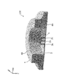
- FIG. 1 is a perspective sectional view showing a configuration of a pressure sensor according to an embodiment of the present invention.
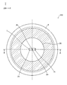
- FIG. 2 is a plan view showing the configuration of the pressure sensor according to the embodiment of the present invention.
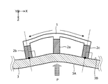
- FIG. 3 is a cross-sectional view showing the configuration of the pressure sensor according to the embodiment of the present invention.
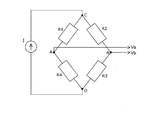
- FIG. 4 is a diagram illustrating a configuration of the bridge circuit.
- FIG. 5 is an enlarged view of the joint portion of the diaphragm, the support member, and the semiconductor chip in FIG.
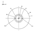
- FIG. 6 is a plan view showing a support surface of the diaphragm.
- FIG. 7 is a diagram schematically showing the displacement of the support member when the diaphragm is deformed.
- FIG. 1 is a perspective sectional view showing a configuration of a pressure sensor according to an embodiment of the present invention.
- FIG. 2 is a plan view showing the configuration of the pressure sensor according to the embodiment of the present invention.
- FIG. 3 is a cross-section
- FIG. 8 is a diagram illustrating the relationship between the radial position of the diaphragm, the amount of diaphragm displacement, and the inclination of the support surface.
- FIG. 9 is a diagram schematically showing displacement of the support member and the semiconductor chip when the diaphragm is deformed.
- FIG. 10 is a diagram for explaining a region where a plurality of resistors are formed in a semiconductor chip.
- FIG. 11 is a diagram illustrating a first arrangement example of resistors in the semiconductor chip.
- FIG. 12 is a diagram illustrating a second arrangement example of resistors in the semiconductor chip.
- FIG. 13 is a diagram showing the variation rate of the span voltage of the bridge circuit with respect to the deviation width of the semiconductor chip in the Y-axis direction.
- FIG. 14 is a diagram for explaining a change in stress of each resistor with respect to a deviation of the semiconductor chip in the X-axis direction.
- the pressure sensor according to the present invention includes a diaphragm (3) having a first main surface (3A) that receives the pressure of a fluid to be measured, and a second main surface (3B) opposite to the first main surface, and a strain.
- a rectangular semiconductor chip (1) having resistors (R1 to R4) constituting a gauge, and one end fixed to the second main surface, the other end fixed to the semiconductor chip, and suspended from the second main surface
- at least three support members (2a, 2b, 2c) made of an insulating material for supporting the semiconductor chip, and one of the support members (2a) is the center of the diaphragm (30
- the other at least two support members (2b, 2c) are provided in the region where the diaphragm is deformed when a pressure larger than the pressure applied to the second main surface is applied to the first main surface.
- Each of the support members Chi at least two other support member may be provided respectively at positions of point symmetry with respect to the center of the diaphragm in a plan view.
- the pressure sensor further includes a housing (4) that accommodates a semiconductor chip, a support member, and a diaphragm and that is formed in a cylindrical shape, and the diaphragm closes an opening at one end (4A) of the housing.
- the at least two other supporting members that are fixed may be provided at positions that do not contact the inner wall (4B) of the housing when a pressure larger than the pressure applied to the second main surface is applied to the first main surface. .
- the at least two other support members are regions in which the inclination of the second main surface is maximized when a pressure larger than the pressure applied to the second main surface is applied to the first main surface and the diaphragm is deformed ( 3D) may be provided.
- the plurality of resistors are formed on the semiconductor chip via the support member when a pressure larger than the pressure applied to the second main surface is applied to the first main surface and the diaphragm is deformed.
- Each of the plurality of resistors may be formed side by side in a direction orthogonal to a direction connecting at least two other support members in plan view.
- the plurality of resistors are formed in regions where tensile stress is generated in the semiconductor chip when a pressure larger than the pressure applied to the second main surface is applied to the first main surface in the semiconductor chip and the diaphragm is deformed.
- the resistors (R1 and R3 and R2 and R4) facing each other in the bridge circuit are respectively formed at positions that are point-symmetric with respect to the center (11) of the semiconductor chip in plan view. May be.
- FIG. 1 shows a perspective sectional structure of a pressure sensor 100 according to the present embodiment.
- FIG. 2 shows a planar structure of the pressure sensor 100 when viewed from the Z direction in FIG.
- FIG. 3 shows a cross-sectional structure of the pressure sensor 100 in the AA cross section of FIG.
- the pressure sensor 100 shown in FIGS. 1 to 3 detects the pressure of the fluid by transmitting the displacement of the diaphragm when the diaphragm is bent by the pressure of the fluid to be measured to the semiconductor chip on which the strain gauge is formed. It is a device to do.
- the pressure sensor 100 has a structure in which the semiconductor chip is supported by at least three support members fixed at positions where displacement on the diaphragm occurs.
- the pressure sensor 100 includes a semiconductor chip 1, support members 2 a to 2 c, a diaphragm 3, and a housing 4. 1 to 3 illustrate a mechanism for transmitting the deflection of the diaphragm 3 in the pressure sensor 100 to the semiconductor chip 1, other functional units such as a circuit for processing a signal output from the semiconductor chip 1 are illustrated. Is omitted.
- the pressure sensor 100 may further include a display unit (for example, a liquid crystal display) for presenting various types of information such as a detected pressure value to the user.
- the semiconductor chip 1, the support members 2a to 2c, and the diaphragm 3 are accommodated in a housing 4 made of a metal material having high corrosion resistance.
- the housing 4 is formed in a cylindrical shape.
- One end 4A of the housing 4 has a joint shape for connection to a pipe through which a fluid to be measured flows.
- the interior of the housing 4 is filled with, for example, air, and the pressure on the inner wall 4B side is, for example, atmospheric pressure.
- the semiconductor chip 1 is composed of a semiconductor substrate such as Si.
- the semiconductor chip 1 has a strain gauge that detects a strain generated by the stress of the semiconductor chip 1 as a change in resistance value.
- the strain gauge is constituted by a bridge circuit 10 composed of, for example, four resistors (for example, diffused resistors) R1 to R4 formed on the semiconductor chip 1.
- the positions where the resistors R1 to R4 are formed in the semiconductor chip 1 will be described in detail later.
- the pressure sensor 100 detects a change in the resistance values of the resistors R1 to R4 due to the stress generated in the semiconductor chip 1 as a change in voltage in a state where a constant current is passed through the bridge circuit 10, whereby the fluid to be measured Can be measured.
- the span voltage Vo output from the bridge circuit 10 can be expressed by the following equation (1) using the resistance values R1 to R4.
- VA and VB represent the voltages at nodes A and B in FIG. 4, respectively, and I represents the current supplied from the constant current source.
- the diaphragm 3 is a film that receives the pressure of the fluid to be measured.
- the diaphragm 3 is made of a material having high corrosion resistance such as stainless steel (SUS), ceramics, and titanium, and is formed in, for example, a circular shape in plan view.
- SUS stainless steel
- the diaphragm 3 supports the semiconductor chip 1 and the support members 2a, 2b, 2c.
- the diaphragm 3 is fixed to the end 4A side of the housing 4 and closes the opening of the end 4A of the housing 4.
- the outer periphery of the diaphragm 3 is joined to the inner wall 4B on the end 4A side of the housing 4 without a gap.
- the diaphragm 3 is a pressure receiving surface (liquid contact surface) 3A that comes into contact with the fluid to be measured and a surface opposite to the pressure receiving surface 3A that supports the semiconductor chip 1 and the support members 2a, 2b, and 2c. Surface 3B.
- the diaphragm 3 bends when a pressure larger than the pressure (for example, atmospheric pressure) applied to the support surface 3B is applied to the pressure receiving surface 3A from the fluid to be measured.
- Support members 2 a, 2 b, 2 c are components that support the semiconductor chip 1 on the diaphragm 3.
- the support member 2 is formed in a columnar shape, for example, a prismatic shape (for example, a quadrangular prism shape).
- the support member 2 is made of an electrically insulating material. More preferably, the support member 2 is made of a material having electrical insulation and low thermal conductivity. Examples of the material of the support member 2 include glass (for example, borosilicate glass (Pyrex (registered trademark))).
- Each of the support members 2a, 2b, and 2c is suspended from the support surface 3B and supports the semiconductor chip 1. Specifically, one end of each of the support members 2 a, 2 b, 2 c is fixed on the support surface 3 ⁇ / b> B of the diaphragm 3, and the other end is fixed to the semiconductor chip 1.
- FIG. 5 is an enlarged view of a joint portion of the diaphragm 3, the support member 2, and the semiconductor chip 1 in FIG. 3.
- one end of the support member 2 a is joined to the central portion of one main surface of the semiconductor chip 1.
- One end portion of the support member 2 b is joined to an end portion on one side of one main surface of the semiconductor chip 1.
- One end of the support member 2 c is joined to the end on the side facing the one side on the one main surface of the semiconductor chip 1.
- FIG. 5 illustrates the case where the bonding portion of the semiconductor chip 1 with the support member 2 is formed thicker in the Z direction than the other portions of the semiconductor chip 1.
- the portion may be the same thickness as the other portions.
- the other ends of the support members 2 a to 2 c are fixed on the support surface 3 B of the diaphragm 3.
- the supporting members 2 a to 2 c are arranged so that the central axes 20 a, 20 b, and 20 c of the supporting members 2 a to 2 c are supported on the supporting surface 3 B ( It is fixed so as to be substantially perpendicular to the (XY plane).
- the positions on the support surface 3B of the diaphragm 3 to which the support members 2a to 2c are fixed are as follows.
- Support member 2a The support member 2a is provided at the center 30 of the diaphragm 3 on the support surface 3B. Specifically, the support member 2a is fixed to the support surface 3B of the diaphragm 3 so that the center of the bottom surface of the support member 2a coincides with the center 30 of the diaphragm 3 in plan view.
- the center 30 of the diaphragm 3 is a point where the displacement of the diaphragm 3 in the Z-axis direction becomes the largest when a pressure larger than the pressure applied to the support surface 3B is applied to the pressure receiving surface 3A.
- the center 30 is the center point of the diaphragm 3 (circle).
- the support member 2a is fixed so that the center of the bottom surface of the support member 2a and the center 30 of the diaphragm 3 coincide with each other on the support surface 3B of the diaphragm 3, but the bottom surface of the support member 2a is fixed.
- the center may be slightly deviated from the center 30 of the diaphragm 3.
- the center of the bottom surface of the support member 2a only needs to be disposed within the range 3C inside the circle centered on the point 30.
- Support members 2b and 2c The support member 2b and the support member 2c have a center 30 (support member 2a) of the diaphragm 3 in plan view in a region where the diaphragm 3 is deformed when a pressure larger than the pressure applied to the support surface 3B is applied to the pressure receiving surface 3A. Are provided at positions that are point-symmetric with respect to each other.
- the ends of the support members 2b and 2c are arranged such that the support members 2b and 2c are inclined with respect to the Z axis when a pressure larger than the pressure applied to the support surface 3B is applied to the pressure receiving surface 3A, and the diaphragm is seen in a plan view. 3 are fixed at positions that are point-symmetric with respect to the center 30 of the three.
- the support members 2b and 2c are inclined with respect to the Z axis and do not contact the inner wall 4B of the housing 4 when a pressure larger than the pressure applied to the support surface 3B is applied to the pressure receiving surface 3A and the diaphragm 3 is deformed. It is provided at each position.
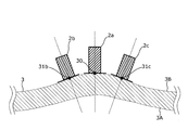
- the inclination (gradient) of the support surface 3B of the diaphragm 3 is maximized. It is provided at each position.
- the position where the inclination of the support surface 3B of the diaphragm 3 is maximum is when the diaphragm 3 is bent as a pressure larger than the pressure applied to the support surface 3B is applied to the pressure receiving surface 3A as shown in FIG. Furthermore, the positions (points 31b and 31c) where the inclination of the support surface 3B of the diaphragm 3 is the largest.
- the point (point 31b, 31c, etc.) where the inclination of the diaphragm 3 is maximum draws a circle 32 having the center 30 of the diaphragm 3 as a center point. Accordingly, by fixing the support members 2b and 2c so that the center of the bottom surface of each of the support members 2b and 2c coincides with two points symmetrical with respect to the center 30 on the circle 32, the displacement of the diaphragm 3 is most reduced. It can be efficiently transmitted to the semiconductor chip 1 and the sensor sensitivity of the pressure sensor 100 can be maximized.
- the support members 2b and 2c when the sensor sensitivity is to be maximized, it is desirable to provide the support members 2b and 2c at the point where the inclination of the diaphragm 3 is maximized, but the position where one end of the support members 2b and 2c is fixed is What is necessary is just to determine suitably in consideration of the required sensor sensitivity and the chip size of the semiconductor chip 1. For example, as shown in FIG. 6, in a peripheral area 3D including a circle 32 drawn by a point where the inclination of the diaphragm 3 is maximum (hereinafter referred to as “area where the inclination of the diaphragm 3 is maximum”) 3D. What is necessary is just to determine the position which fixes the end of support member 2b, 2c. Specific examples are shown below.
- FIG. 8 is a diagram showing the relationship between the radial position of the diaphragm, the displacement of the diaphragm, and the inclination of the support surface.
- the horizontal axis represents the relative distance from the center of the diaphragm 3 when the radius of the diaphragm 3 is “1”
- the vertical axis is the relative distance when the maximum displacement of the diaphragm 3 is “1”.
- the amount of relative displacement and the relative inclination when the maximum value of the inclination of the diaphragm 3 is “1”.
- reference numeral 301 represents the amount of displacement of the diaphragm 3 according to the relative distance from the center of the diaphragm 3
- reference numeral 302 represents the support of the diaphragm 3 according to the relative distance from the center of the diaphragm 3. It represents the inclination of the surface 3B.
- the inclination of the diaphragm 3 is the largest at the points 31b and 31c of the diaphragm 3, but the relative distance from the center of the diaphragm 3 is in the range of “0.35 to 0.77”. Also, an inclination of 80% or more with respect to the maximum inclination is obtained. Therefore, for example, if this range is set to a region 3D where the inclination of the diaphragm 3 is maximum, and one end of each of the support members 2b and 2c is fixed so that the centers of the bottom surfaces of the support members 2b and 2c are located in the region 3D. The sensitivity of the sensor can be increased.
- the support members 2b and 2c are arranged in a region (for example, a relative distance of “0.35 to 0.50”) inside the circle 32 in the region 3D where the inclination of the support surface 3B of the diaphragm 3 is maximum.
- a region for example, a relative distance of “0.35 to 0.50” inside the circle 32 in the region 3D where the inclination of the support surface 3B of the diaphragm 3 is maximum.
- the semiconductor chip 1 can be further miniaturized while maintaining the sensitivity of the sensor.
- FIG. 9 is a diagram schematically showing displacement of the support member 2 and the semiconductor chip 1 when the diaphragm 3 is deformed.
- the other ends of the support members 2b and 2c are displaced not only in the Z-axis direction but also in the X-axis direction. More specifically, the support members 2b and 2c are inclined in directions in which the other ends thereof are separated from the center 30 (support member 2a) of the diaphragm 3, that is, in a direction approaching the inner wall 4B of the housing 4.
- the semiconductor chip 1 is pulled outward, and a tensile stress is generated inside the semiconductor chip 1. That is, a tensile stress corresponding to the displacement difference between the support member 2 a and the support member 2 b in the X-axis direction and the Y-axis direction is generated inside the semiconductor chip 1. Therefore, the pressure of the fluid to be measured can be detected with high accuracy by appropriately forming the resistors R1 to R4 constituting the strain gauge (bridge circuit) in the region where the tensile stress is generated in the semiconductor chip 1. It becomes possible to do.
- FIG. 10 is a diagram for explaining a region where the resistors R1 to R4 are formed in the semiconductor chip 1.
- a plan view of the semiconductor chip 1 is shown in the lower part of FIG. 10, the horizontal axis represents the distance in the X-axis direction corresponding to the plan view of the lower semiconductor chip 1 in FIG. 10, and the vertical axis represents the stress generated inside the semiconductor chip 1 when the diaphragm 3 is bent.
- the graph is shown.
- the resistors R1 to R4 have a tensile stress in the region where the stress generated in the semiconductor chip 1 becomes positive (+) when the diaphragm 3 is bent by the pressure of the fluid, that is, in the semiconductor chip 1.
- the locations of the resistors R1 to R4 in the regions 10ab and 10ac are not particularly limited. For example, it is desirable to arrange the resistors R1 to R4 as shown in FIGS.
- the resistors R1 to R4 have a tensile stress applied to the semiconductor chip 1 via the support member 2 when a pressure larger than the pressure applied to the support surface 3B is applied to the pressure receiving surface 3A and the diaphragm 3 is deformed.
- produces you may form side by side in the direction (Y-axis direction) orthogonal to the direction which connects two support member 2b, 2c by planar view.
- the resistors R1 to R4 may be formed side by side in the short direction of the semiconductor chip in one of the region 10ab and the region 10ac of the semiconductor chip 1.
- the resistors facing each other in the bridge circuit 10 are respectively formed at positions that are point-symmetric with respect to the center 11 of the semiconductor chip 1 in plan view. Also good. More specifically, the resistors R1 and R3 may be arranged point-symmetrically with respect to the center 11 of the semiconductor chip 1 in plan view. Further, the resistor R2 and the resistor R4 may be arranged point-symmetrically with respect to the center 11 of the semiconductor chip 1 in plan view.
- FIG. 13 is a simulation result showing the fluctuation of the span voltage of the bridge circuit with respect to the positional deviation in the Y-axis direction with respect to the diaphragm 3 of the semiconductor chip 1 when the resistors R1 to R4 are arranged as shown in FIG.
- the horizontal axis represents the ratio of the deviation width of the semiconductor chip 1 to the diameter of the diaphragm 3
- the vertical axis represents the variation rate [% FS] of the span voltage of the bridge circuit composed of the resistors R1 to R4.
- the deviation in the short direction (Y-axis direction) of the semiconductor chip 1 with respect to the diameter of the diaphragm 3 is ⁇ 5.
- the fluctuation of the span voltage can be suppressed within 1% FS.
- the tolerance of the positional deviation of the semiconductor chip 1 with respect to the diaphragm 3 in the Y-axis direction can be increased. This effect is also obtained when the opposing resistors in the bridge circuit 10 are formed at positions that are point-symmetric with respect to the center 11 of the semiconductor chip 1 (see FIG. 12).
- FIG. 14 is a diagram showing the variation rate of the span voltage of the bridge circuit with respect to the deviation width of the semiconductor chip in the Y-axis direction.
- FIG. 14 shows a simulation result of the stress distribution of the semiconductor chip 1 when pressure is applied to the semiconductor chip 1 in which the resistors R1 to R4 are arranged as shown in FIG.
- the horizontal axis represents the position in the X-axis direction from the center 30 of the diaphragm 3
- the vertical axis represents the stress of the semiconductor chip 1.
- the pressure sensor according to the present invention includes the support member 2a fixed substantially perpendicular to the support surface 3B at the center 30 of the diaphragm 3, and the center 30 of the diaphragm in the region where the diaphragm 3 is deformed.
- the semiconductor chip on which the strain gauge is formed is supported by the two support members 2b and 2c fixed substantially perpendicular to the support surface 3B at a point-symmetrical position.
- the support members 2b and 2c arranged on both sides of the support member 2a are inclined outward, so that the tensile stress corresponding to the displacement of the diaphragm 3 is applied to the semiconductor chip 1. It can be efficiently generated inside.
- the pressure sensor 100 since the support members 2b and 2c that support both ends of the semiconductor chip are fixed to the region where the diaphragm 3 is deformed, it is substantially the same as a conventional load conversion type pressure sensor.
- the chip size of the semiconductor chip can be reduced as compared with the case where the support members 2b and 2c are fixed at a position where the support member 2b or 2c is not located at the position where the diaphragm 3 is deformed.
- the pressure sensor 100 of the present invention it is possible to achieve both miniaturization and high sensitivity of the semiconductor chip.
- the support members 2b and 2c are positioned so that the support members 2b and 2c are inclined with respect to the Z axis and do not contact the inner wall 4B of the housing 4 when the diaphragm 3 is bent by the pressure from the fluid. Secure to. According to this, since the inclination of the support members 2b and 2c is not limited by the inner wall 4B of the housing 4, the pressure range that can be detected by the pressure sensor 100 can be expanded.
- the sensor sensitivity can be further improved as described above. Further, by fixing the support members 2b and 2c to the region 3D where the inclination of the diaphragm 3 is maximum, as described above, the semiconductor chip can be further miniaturized while maintaining high sensor sensitivity.
- the resistors R1 to R4 constituting the bridge circuit 100 are arranged side by side in the short-side direction of the semiconductor chip 1 in the region where the tensile stress is generated in the semiconductor chip 1 as described above.
- the tolerance of the positional deviation of the semiconductor chip 1 with respect to the diaphragm 3 in the short direction can be increased. Thereby, high sensitivity of the pressure sensor 100 can be expected.
- the opposing resistors in the bridge circuit 10 are formed at positions that are point-symmetric with respect to the center 11 of the semiconductor chip 1 in a region where tensile stress is generated in the semiconductor chip 1 (see FIG. 12), As described above, not only the tolerance of the positional deviation of the semiconductor chip 1 in the Y-axis direction with respect to the diaphragm 3 can be increased, but also the influence of the positional deviation of the semiconductor chip 1 in the X-axis direction with respect to the diaphragm 3 can be reduced. it can. Thereby, further high sensitivity of the pressure sensor 100 can be expected.
- the support member 2 has a prismatic shape
- the support member 2 may have a columnar shape, for example.
- the pressure sensor according to the present invention can be applied to various uses such as a sanitary pressure sensor.
- SYMBOLS 100 Pressure sensor, 1 ... Semiconductor chip, 2, 2a, 2b, 2c ... Support member, 3 ... Diaphragm, 3A ... Pressure-receiving surface, 3B ... Support surface, 3C ... Center area
Landscapes
- Physics & Mathematics (AREA)
- General Physics & Mathematics (AREA)
- Measuring Fluid Pressure (AREA)
- Pressure Sensors (AREA)
Abstract
La présente invention concerne un capteur de pression qui comprend : un diaphragme (3) ayant une première surface principale (3A) et une deuxième surface principale (3B) qui est située sur le côté opposé à la première surface principale (3A) ; et au moins trois éléments de support (2a, 2b, 2c) constitués d'un matériau isolant, les au moins trois éléments de support (2a, 2b, 2c) comportant chacun une extrémité fixée à la deuxième surface principale et l'autre extrémité fixée à une puce à semi-conducteur (1), les au moins trois éléments de support (2a, 2b, 2c) s'étendant vers le bas vers la deuxième surface principale et soutenant la puce à semi-conducteur. Le capteur de pression est caractérisé en ce que : un élément de support (2a) des éléments de support est disposé au centre (30) du diaphragme dans une vue plane ; et les au moins deux éléments de support restants (2b, 2c) sont situés dans une région du diaphragme à des positions en symétrie ponctuelle par rapport au centre du diaphragme dans la vue plane, la région se déformant lorsqu'une pression plus élevée que la pression exercée sur la deuxième surface principale est appliquée à la première surface principale.
Priority Applications (2)
| Application Number | Priority Date | Filing Date | Title |
|---|---|---|---|
| US16/066,565 US10704976B2 (en) | 2015-12-28 | 2016-12-15 | Pressure sensor |
| CN201680076345.2A CN108474704B (zh) | 2015-12-28 | 2016-12-15 | 压力传感器 |
Applications Claiming Priority (2)
| Application Number | Priority Date | Filing Date | Title |
|---|---|---|---|
| JP2015-256377 | 2015-12-28 | ||
| JP2015256377A JP6581900B2 (ja) | 2015-12-28 | 2015-12-28 | 圧力センサ |
Publications (1)
| Publication Number | Publication Date |
|---|---|
| WO2017115660A1 true WO2017115660A1 (fr) | 2017-07-06 |
Family
ID=59225085
Family Applications (1)
| Application Number | Title | Priority Date | Filing Date |
|---|---|---|---|
| PCT/JP2016/087346 Ceased WO2017115660A1 (fr) | 2015-12-28 | 2016-12-15 | Capteur de pression |
Country Status (4)
| Country | Link |
|---|---|
| US (1) | US10704976B2 (fr) |
| JP (1) | JP6581900B2 (fr) |
| CN (1) | CN108474704B (fr) |
| WO (1) | WO2017115660A1 (fr) |
Families Citing this family (6)
| Publication number | Priority date | Publication date | Assignee | Title |
|---|---|---|---|---|
| JP6579965B2 (ja) * | 2016-01-19 | 2019-09-25 | アズビル株式会社 | 圧力センサ |
| JP6663314B2 (ja) * | 2016-07-08 | 2020-03-11 | アズビル株式会社 | 圧力センサ |
| CN110895130B (zh) * | 2019-12-28 | 2021-07-20 | 中航电测仪器股份有限公司 | 一种膜片式应变计及其优化方法 |
| JP7436218B2 (ja) * | 2020-01-27 | 2024-02-21 | アズビル株式会社 | 圧力センサ |
| JP7440290B2 (ja) * | 2020-02-19 | 2024-02-28 | アズビル株式会社 | 圧力センサ |
| CN116124350A (zh) * | 2022-12-26 | 2023-05-16 | 中航光电华亿(沈阳)电子科技有限公司 | 压力传感器芯体及其制作方法 |
Citations (7)
| Publication number | Priority date | Publication date | Assignee | Title |
|---|---|---|---|---|
| JPS63217671A (ja) * | 1987-03-05 | 1988-09-09 | Nippon Denso Co Ltd | 半導体圧力センサ |
| JPH09232595A (ja) * | 1996-02-26 | 1997-09-05 | Denso Corp | 圧力検出装置 |
| JP2000508425A (ja) * | 1996-04-13 | 2000-07-04 | ローベルト ボツシユ ゲゼルシヤフト ミツト ベシユレンクテル ハフツング | 圧力センサ |
| EP1876434A2 (fr) * | 2006-07-05 | 2008-01-09 | HYDAC Electronic GmbH | Dispositif destiné à la mesure de forces, en particulier un capteur de pression, et procédé de fabrication correspondant |
| US20130305834A1 (en) * | 2011-01-12 | 2013-11-21 | Wolfgang Brode | Device for converting a force or a pressure into an electrical signal and method for producing such a device |
| DE102013209385A1 (de) * | 2013-05-22 | 2014-11-27 | Robert Bosch Gmbh | Mikromechanische Differenzdrucksensorvorrichtung, entsprechendes Herstellungsverfahren und Differenzdrucksensoranordnung |
| DE102014118850A1 (de) * | 2014-12-17 | 2016-06-23 | Endress + Hauser Gmbh + Co. Kg | Drucksensor zur Messung eines Differenzdrucks und eines Systemdrucks |
Family Cites Families (10)
| Publication number | Priority date | Publication date | Assignee | Title |
|---|---|---|---|---|
| CN1024842C (zh) * | 1989-08-25 | 1994-06-01 | 株式会社长野计器制作所 | 应变检测元件及使用它的压力变换器 |
| JP2004045140A (ja) | 2002-07-10 | 2004-02-12 | Tem-Tech Kenkyusho:Kk | 荷重変換型の金属ダイヤフラム圧力センサ |
| DE102005001298A1 (de) * | 2005-01-03 | 2006-07-13 | Hydac Electronic Gmbh | Vorrichtung zum Messen von Kräften, insbesondere Drucksensor, und zugehöriges Herstellverfahren |
| CN101000271A (zh) * | 2006-01-10 | 2007-07-18 | 昆山双桥传感器测控技术有限公司 | 抗腐蚀的压力传感器 |
| DE102009001133A1 (de) * | 2009-02-25 | 2010-08-26 | Endress + Hauser Gmbh + Co. Kg | Drucksensor mit Halbleiterdruckmesswandler |
| JP2013526083A (ja) * | 2010-05-03 | 2013-06-20 | エス3シー インコーポレイテッド | ウエハ上のmemsダイ分離時のチッピングを最小にする方法 |
| JP5418618B2 (ja) * | 2011-03-23 | 2014-02-19 | 株式会社デンソー | 圧力センサ |
| CN202974522U (zh) * | 2012-11-01 | 2013-06-05 | 中国科学院半导体研究所 | 一种基于双l型梁的光纤光栅土压力传感器 |
| JP5839150B2 (ja) * | 2013-05-24 | 2016-01-06 | 日立金属株式会社 | 圧力センサ及びそれを用いたマスフローメータ並びにマスフローコントローラ |
| CN105092117B (zh) * | 2015-08-19 | 2017-06-09 | 东南大学 | 一种压阻式压力传感器及其制备方法 |
-
2015
- 2015-12-28 JP JP2015256377A patent/JP6581900B2/ja active Active
-
2016
- 2016-12-15 US US16/066,565 patent/US10704976B2/en active Active
- 2016-12-15 CN CN201680076345.2A patent/CN108474704B/zh active Active
- 2016-12-15 WO PCT/JP2016/087346 patent/WO2017115660A1/fr not_active Ceased
Patent Citations (7)
| Publication number | Priority date | Publication date | Assignee | Title |
|---|---|---|---|---|
| JPS63217671A (ja) * | 1987-03-05 | 1988-09-09 | Nippon Denso Co Ltd | 半導体圧力センサ |
| JPH09232595A (ja) * | 1996-02-26 | 1997-09-05 | Denso Corp | 圧力検出装置 |
| JP2000508425A (ja) * | 1996-04-13 | 2000-07-04 | ローベルト ボツシユ ゲゼルシヤフト ミツト ベシユレンクテル ハフツング | 圧力センサ |
| EP1876434A2 (fr) * | 2006-07-05 | 2008-01-09 | HYDAC Electronic GmbH | Dispositif destiné à la mesure de forces, en particulier un capteur de pression, et procédé de fabrication correspondant |
| US20130305834A1 (en) * | 2011-01-12 | 2013-11-21 | Wolfgang Brode | Device for converting a force or a pressure into an electrical signal and method for producing such a device |
| DE102013209385A1 (de) * | 2013-05-22 | 2014-11-27 | Robert Bosch Gmbh | Mikromechanische Differenzdrucksensorvorrichtung, entsprechendes Herstellungsverfahren und Differenzdrucksensoranordnung |
| DE102014118850A1 (de) * | 2014-12-17 | 2016-06-23 | Endress + Hauser Gmbh + Co. Kg | Drucksensor zur Messung eines Differenzdrucks und eines Systemdrucks |
Also Published As
| Publication number | Publication date |
|---|---|
| US10704976B2 (en) | 2020-07-07 |
| CN108474704B (zh) | 2020-06-02 |
| US20190003910A1 (en) | 2019-01-03 |
| JP2017120214A (ja) | 2017-07-06 |
| JP6581900B2 (ja) | 2019-09-25 |
| CN108474704A (zh) | 2018-08-31 |
Similar Documents
| Publication | Publication Date | Title |
|---|---|---|
| JP6581900B2 (ja) | 圧力センサ | |
| JP6663315B2 (ja) | 圧力センサ | |
| CN107152982B (zh) | 压力传感器芯片及压力传感器 | |
| CN102435383A (zh) | 压力传感器 | |
| US9891119B2 (en) | Sensor, strain sensor, and pressure sensor | |
| US20120160029A1 (en) | Acceleration sensor | |
| CN103901227B (zh) | 硅微谐振式加速度计 | |
| US9857258B2 (en) | Pressure sensor to sense multi-directional movement | |
| JP2009002834A (ja) | 角速度検出装置 | |
| CN107588882B (zh) | 压力传感器 | |
| JP6521876B2 (ja) | 圧力センサ | |
| CN109270298B (zh) | Mems加速度计 | |
| JP6579965B2 (ja) | 圧力センサ | |
| JP2017120211A (ja) | 圧力センサ | |
| JP5821158B1 (ja) | 複合センサデバイス | |
| JP2017120212A (ja) | 圧力センサ | |
| CN107735660B (zh) | 用于检测机械解耦压力的装置 | |
| JP2017120213A (ja) | 圧力センサ | |
| JPH0526754A (ja) | 静電容量の変化を利用したセンサ | |
| JP2013104754A (ja) | 物理量検出器および物理量検出器の製造方法 | |
| CN104797942A (zh) | 角加速度传感器及加速度传感器 | |
| JPH06174509A (ja) | カルマン渦流量計 |
Legal Events
| Date | Code | Title | Description |
|---|---|---|---|
| 121 | Ep: the epo has been informed by wipo that ep was designated in this application |
Ref document number: 16881638 Country of ref document: EP Kind code of ref document: A1 |
|
| NENP | Non-entry into the national phase |
Ref country code: DE |
|
| 122 | Ep: pct application non-entry in european phase |
Ref document number: 16881638 Country of ref document: EP Kind code of ref document: A1 |