WO2017122792A1 - Module de laser à semi-conducteur et procédé de fabrication de module de laser à semi-conducteur - Google Patents
Module de laser à semi-conducteur et procédé de fabrication de module de laser à semi-conducteur Download PDFInfo
- Publication number
- WO2017122792A1 WO2017122792A1 PCT/JP2017/001058 JP2017001058W WO2017122792A1 WO 2017122792 A1 WO2017122792 A1 WO 2017122792A1 JP 2017001058 W JP2017001058 W JP 2017001058W WO 2017122792 A1 WO2017122792 A1 WO 2017122792A1
- Authority
- WO
- WIPO (PCT)
- Prior art keywords
- semiconductor laser
- rows
- laser installation
- installation
- semiconductor
- Prior art date
- Legal status (The legal status is an assumption and is not a legal conclusion. Google has not performed a legal analysis and makes no representation as to the accuracy of the status listed.)
- Ceased
Links
Images




Classifications
-
- H—ELECTRICITY
- H01—ELECTRIC ELEMENTS
- H01S—DEVICES USING THE PROCESS OF LIGHT AMPLIFICATION BY STIMULATED EMISSION OF RADIATION [LASER] TO AMPLIFY OR GENERATE LIGHT; DEVICES USING STIMULATED EMISSION OF ELECTROMAGNETIC RADIATION IN WAVE RANGES OTHER THAN OPTICAL
- H01S5/00—Semiconductor lasers
- H01S5/02—Structural details or components not essential to laser action
- H01S5/022—Mountings; Housings
- H01S5/023—Mount members, e.g. sub-mount members
- H01S5/02325—Mechanically integrated components on mount members or optical micro-benches
- H01S5/02326—Arrangements for relative positioning of laser diodes and optical components, e.g. grooves in the mount to fix optical fibres or lenses
-
- G—PHYSICS
- G02—OPTICS
- G02B—OPTICAL ELEMENTS, SYSTEMS OR APPARATUS
- G02B27/00—Optical systems or apparatus not provided for by any of the groups G02B1/00 - G02B26/00, G02B30/00
- G02B27/09—Beam shaping, e.g. changing the cross-sectional area, not otherwise provided for
- G02B27/0916—Adapting the beam shape of a semiconductor light source such as a laser diode or an LED, e.g. for efficiently coupling into optical fibers
- G02B27/0922—Adapting the beam shape of a semiconductor light source such as a laser diode or an LED, e.g. for efficiently coupling into optical fibers the semiconductor light source comprising an array of light emitters
-
- G—PHYSICS
- G02—OPTICS
- G02B—OPTICAL ELEMENTS, SYSTEMS OR APPARATUS
- G02B27/00—Optical systems or apparatus not provided for by any of the groups G02B1/00 - G02B26/00, G02B30/00
- G02B27/10—Beam splitting or combining systems
- G02B27/106—Beam splitting or combining systems for splitting or combining a plurality of identical beams or images, e.g. image replication
-
- G—PHYSICS
- G02—OPTICS
- G02B—OPTICAL ELEMENTS, SYSTEMS OR APPARATUS
- G02B6/00—Light guides; Structural details of arrangements comprising light guides and other optical elements, e.g. couplings
- G02B6/24—Coupling light guides
- G02B6/42—Coupling light guides with opto-electronic elements
-
- G—PHYSICS
- G02—OPTICS
- G02B—OPTICAL ELEMENTS, SYSTEMS OR APPARATUS
- G02B6/00—Light guides; Structural details of arrangements comprising light guides and other optical elements, e.g. couplings
- G02B6/24—Coupling light guides
- G02B6/42—Coupling light guides with opto-electronic elements
- G02B6/4201—Packages, e.g. shape, construction, internal or external details
- G02B6/4204—Packages, e.g. shape, construction, internal or external details the coupling comprising intermediate optical elements, e.g. lenses, holograms
- G02B6/4206—Optical features
-
- G—PHYSICS
- G02—OPTICS
- G02B—OPTICAL ELEMENTS, SYSTEMS OR APPARATUS
- G02B6/00—Light guides; Structural details of arrangements comprising light guides and other optical elements, e.g. couplings
- G02B6/24—Coupling light guides
- G02B6/42—Coupling light guides with opto-electronic elements
- G02B6/4201—Packages, e.g. shape, construction, internal or external details
- G02B6/4204—Packages, e.g. shape, construction, internal or external details the coupling comprising intermediate optical elements, e.g. lenses, holograms
- G02B6/4214—Packages, e.g. shape, construction, internal or external details the coupling comprising intermediate optical elements, e.g. lenses, holograms the intermediate optical element having redirecting reflective means, e.g. mirrors, prisms for deflecting the radiation from horizontal to down- or upward direction toward a device
-
- H—ELECTRICITY
- H01—ELECTRIC ELEMENTS
- H01S—DEVICES USING THE PROCESS OF LIGHT AMPLIFICATION BY STIMULATED EMISSION OF RADIATION [LASER] TO AMPLIFY OR GENERATE LIGHT; DEVICES USING STIMULATED EMISSION OF ELECTROMAGNETIC RADIATION IN WAVE RANGES OTHER THAN OPTICAL
- H01S5/00—Semiconductor lasers
- H01S5/02—Structural details or components not essential to laser action
- H01S5/022—Mountings; Housings
- H01S5/0239—Combinations of electrical or optical elements
-
- H—ELECTRICITY
- H01—ELECTRIC ELEMENTS
- H01S—DEVICES USING THE PROCESS OF LIGHT AMPLIFICATION BY STIMULATED EMISSION OF RADIATION [LASER] TO AMPLIFY OR GENERATE LIGHT; DEVICES USING STIMULATED EMISSION OF ELECTROMAGNETIC RADIATION IN WAVE RANGES OTHER THAN OPTICAL
- H01S5/00—Semiconductor lasers
- H01S5/40—Arrangement of two or more semiconductor lasers, not provided for in groups H01S5/02 - H01S5/30
-
- H—ELECTRICITY
- H01—ELECTRIC ELEMENTS
- H01S—DEVICES USING THE PROCESS OF LIGHT AMPLIFICATION BY STIMULATED EMISSION OF RADIATION [LASER] TO AMPLIFY OR GENERATE LIGHT; DEVICES USING STIMULATED EMISSION OF ELECTROMAGNETIC RADIATION IN WAVE RANGES OTHER THAN OPTICAL
- H01S5/00—Semiconductor lasers
- H01S5/40—Arrangement of two or more semiconductor lasers, not provided for in groups H01S5/02 - H01S5/30
- H01S5/4012—Beam combining, e.g. by the use of fibres, gratings, polarisers, prisms
-
- H—ELECTRICITY
- H01—ELECTRIC ELEMENTS
- H01S—DEVICES USING THE PROCESS OF LIGHT AMPLIFICATION BY STIMULATED EMISSION OF RADIATION [LASER] TO AMPLIFY OR GENERATE LIGHT; DEVICES USING STIMULATED EMISSION OF ELECTROMAGNETIC RADIATION IN WAVE RANGES OTHER THAN OPTICAL
- H01S5/00—Semiconductor lasers
- H01S5/40—Arrangement of two or more semiconductor lasers, not provided for in groups H01S5/02 - H01S5/30
- H01S5/4025—Array arrangements, e.g. constituted by discrete laser diodes or laser bar
-
- H—ELECTRICITY
- H01—ELECTRIC ELEMENTS
- H01S—DEVICES USING THE PROCESS OF LIGHT AMPLIFICATION BY STIMULATED EMISSION OF RADIATION [LASER] TO AMPLIFY OR GENERATE LIGHT; DEVICES USING STIMULATED EMISSION OF ELECTROMAGNETIC RADIATION IN WAVE RANGES OTHER THAN OPTICAL
- H01S5/00—Semiconductor lasers
- H01S5/40—Arrangement of two or more semiconductor lasers, not provided for in groups H01S5/02 - H01S5/30
- H01S5/4025—Array arrangements, e.g. constituted by discrete laser diodes or laser bar
- H01S5/4031—Edge-emitting structures
- H01S5/4043—Edge-emitting structures with vertically stacked active layers
- H01S5/405—Two-dimensional arrays
-
- H—ELECTRICITY
- H01—ELECTRIC ELEMENTS
- H01S—DEVICES USING THE PROCESS OF LIGHT AMPLIFICATION BY STIMULATED EMISSION OF RADIATION [LASER] TO AMPLIFY OR GENERATE LIGHT; DEVICES USING STIMULATED EMISSION OF ELECTROMAGNETIC RADIATION IN WAVE RANGES OTHER THAN OPTICAL
- H01S5/00—Semiconductor lasers
- H01S5/40—Arrangement of two or more semiconductor lasers, not provided for in groups H01S5/02 - H01S5/30
- H01S5/4025—Array arrangements, e.g. constituted by discrete laser diodes or laser bar
- H01S5/4031—Edge-emitting structures
- H01S5/4056—Edge-emitting structures emitting light in more than one direction
-
- H—ELECTRICITY
- H01—ELECTRIC ELEMENTS
- H01S—DEVICES USING THE PROCESS OF LIGHT AMPLIFICATION BY STIMULATED EMISSION OF RADIATION [LASER] TO AMPLIFY OR GENERATE LIGHT; DEVICES USING STIMULATED EMISSION OF ELECTROMAGNETIC RADIATION IN WAVE RANGES OTHER THAN OPTICAL
- H01S5/00—Semiconductor lasers
- H01S5/40—Arrangement of two or more semiconductor lasers, not provided for in groups H01S5/02 - H01S5/30
- H01S5/4025—Array arrangements, e.g. constituted by discrete laser diodes or laser bar
- H01S5/4081—Near-or far field control
-
- G—PHYSICS
- G02—OPTICS
- G02B—OPTICAL ELEMENTS, SYSTEMS OR APPARATUS
- G02B27/00—Optical systems or apparatus not provided for by any of the groups G02B1/00 - G02B26/00, G02B30/00
- G02B27/09—Beam shaping, e.g. changing the cross-sectional area, not otherwise provided for
- G02B27/0938—Using specific optical elements
- G02B27/095—Refractive optical elements
- G02B27/0955—Lenses
- G02B27/0961—Lens arrays
-
- G—PHYSICS
- G02—OPTICS
- G02B—OPTICAL ELEMENTS, SYSTEMS OR APPARATUS
- G02B27/00—Optical systems or apparatus not provided for by any of the groups G02B1/00 - G02B26/00, G02B30/00
- G02B27/09—Beam shaping, e.g. changing the cross-sectional area, not otherwise provided for
- G02B27/0938—Using specific optical elements
- G02B27/095—Refractive optical elements
- G02B27/0955—Lenses
- G02B27/0966—Cylindrical lenses
-
- G—PHYSICS
- G02—OPTICS
- G02B—OPTICAL ELEMENTS, SYSTEMS OR APPARATUS
- G02B27/00—Optical systems or apparatus not provided for by any of the groups G02B1/00 - G02B26/00, G02B30/00
- G02B27/10—Beam splitting or combining systems
- G02B27/12—Beam splitting or combining systems operating by refraction only
- G02B27/123—The splitting element being a lens or a system of lenses, including arrays and surfaces with refractive power
-
- H—ELECTRICITY
- H01—ELECTRIC ELEMENTS
- H01S—DEVICES USING THE PROCESS OF LIGHT AMPLIFICATION BY STIMULATED EMISSION OF RADIATION [LASER] TO AMPLIFY OR GENERATE LIGHT; DEVICES USING STIMULATED EMISSION OF ELECTROMAGNETIC RADIATION IN WAVE RANGES OTHER THAN OPTICAL
- H01S5/00—Semiconductor lasers
- H01S5/02—Structural details or components not essential to laser action
- H01S5/022—Mountings; Housings
- H01S5/02208—Mountings; Housings characterised by the shape of the housings
- H01S5/02216—Butterfly-type, i.e. with electrode pins extending horizontally from the housings
-
- H—ELECTRICITY
- H01—ELECTRIC ELEMENTS
- H01S—DEVICES USING THE PROCESS OF LIGHT AMPLIFICATION BY STIMULATED EMISSION OF RADIATION [LASER] TO AMPLIFY OR GENERATE LIGHT; DEVICES USING STIMULATED EMISSION OF ELECTROMAGNETIC RADIATION IN WAVE RANGES OTHER THAN OPTICAL
- H01S5/00—Semiconductor lasers
- H01S5/02—Structural details or components not essential to laser action
- H01S5/022—Mountings; Housings
- H01S5/0225—Out-coupling of light
-
- H—ELECTRICITY
- H01—ELECTRIC ELEMENTS
- H01S—DEVICES USING THE PROCESS OF LIGHT AMPLIFICATION BY STIMULATED EMISSION OF RADIATION [LASER] TO AMPLIFY OR GENERATE LIGHT; DEVICES USING STIMULATED EMISSION OF ELECTROMAGNETIC RADIATION IN WAVE RANGES OTHER THAN OPTICAL
- H01S5/00—Semiconductor lasers
- H01S5/02—Structural details or components not essential to laser action
- H01S5/022—Mountings; Housings
- H01S5/0225—Out-coupling of light
- H01S5/02251—Out-coupling of light using optical fibres
-
- H—ELECTRICITY
- H01—ELECTRIC ELEMENTS
- H01S—DEVICES USING THE PROCESS OF LIGHT AMPLIFICATION BY STIMULATED EMISSION OF RADIATION [LASER] TO AMPLIFY OR GENERATE LIGHT; DEVICES USING STIMULATED EMISSION OF ELECTROMAGNETIC RADIATION IN WAVE RANGES OTHER THAN OPTICAL
- H01S5/00—Semiconductor lasers
- H01S5/02—Structural details or components not essential to laser action
- H01S5/022—Mountings; Housings
- H01S5/0225—Out-coupling of light
- H01S5/02253—Out-coupling of light using lenses
-
- H—ELECTRICITY
- H01—ELECTRIC ELEMENTS
- H01S—DEVICES USING THE PROCESS OF LIGHT AMPLIFICATION BY STIMULATED EMISSION OF RADIATION [LASER] TO AMPLIFY OR GENERATE LIGHT; DEVICES USING STIMULATED EMISSION OF ELECTROMAGNETIC RADIATION IN WAVE RANGES OTHER THAN OPTICAL
- H01S5/00—Semiconductor lasers
- H01S5/02—Structural details or components not essential to laser action
- H01S5/022—Mountings; Housings
- H01S5/0225—Out-coupling of light
- H01S5/02255—Out-coupling of light using beam deflecting elements
Definitions
- the present invention relates to a semiconductor laser module and the like that are compact and easy to assemble.
- a semiconductor laser module that couples light output from a plurality of semiconductor lasers to an optical fiber.
- a plurality of semiconductor lasers are provided in the housing of the semiconductor laser module. Therefore, as the number of semiconductor lasers installed increases, the length of the semiconductor laser module increases. For this reason, a more compact semiconductor laser module is required.
- a semiconductor laser module for example, a plurality of lasers are arranged so as to face each other, and lenses and mirrors corresponding to the respective semiconductor lasers are arranged in a plurality of stages in the height direction and coupled to an optical fiber.
- a semiconductor laser module for example, Patent Document 1.
- FIG. 8 is a plan view showing a conventional semiconductor laser module 100 as disclosed in Patent Document 1.
- FIG. FIG. 8 is a perspective view of the upper surface of the housing 103.
- the semiconductor laser module 100 mainly includes a housing 103, a semiconductor laser 105, lenses 107 and 109, a reflection mirror 111, a condenser lens 115, an optical fiber 119, and the like.
- a semiconductor laser 105 Inside the housing 103, a semiconductor laser 105, lenses 107 and 109, a reflection mirror 111, a condenser lens 115, an optical fiber 119, and the like are arranged.
- the semiconductor lasers 105 are arranged in a plurality of rows in order to increase the loading efficiency of the semiconductor lasers 105. That is, a plurality of semiconductor laser installation rows 121a and 121b are provided.
- the bottom of the housing 103 is formed in a staircase shape so that the height gradually increases.
- Each step is a semiconductor laser installation surface 117.
- a semiconductor laser 105 is installed on each semiconductor laser installation surface 117.
- the semiconductor lasers 105 of the respective semiconductor laser installation rows 121a and 121b are arranged on the semiconductor laser installation surface 117 at different heights. Therefore, the semiconductor lasers 105 arranged in the semiconductor laser installation rows 121a and 121b are all arranged at different heights at a constant pitch.
- a lens 107 is disposed in front of the semiconductor laser 105 (outgoing direction). Further, a lens 109 is arranged in front of the lens. The lenses 107 and 109 collimate the light emitted from the semiconductor laser 105 in the vertical direction and the horizontal direction, respectively. The lenses 107 and 109 are arranged for each semiconductor laser 105.
- the semiconductor lasers 105 of the respective semiconductor laser installation rows 121 a and 121 b are arranged so as to face each other, and the laser is irradiated toward the center in the width direction of the housing 103.
- the reflection mirrors 111 are arranged in a substantially line.
- the reflection mirror 111 is disposed on the installation surface having the same height as the corresponding semiconductor laser 105.
- the light emitted from the semiconductor lasers 105 of the semiconductor laser installation rows 121a and 121b and collimated by the lenses 107 and 109 is reflected by the reflection mirror 111 and changes its direction substantially vertically. At this time, the light emitted from the semiconductor laser 105 in the semiconductor laser installation row 121a and the light emitted from the semiconductor laser 105 in the semiconductor laser installation row 121b are reflected on the same axis when viewed from above.
- the light (beam group 123) reflected by the respective reflecting mirrors 111 is collected by the condenser lens 115 and optically coupled to the optical fiber 119.
- FIG. 9 is a conceptual diagram showing the arrangement of the semiconductor laser 105 and the reflection mirror 111.
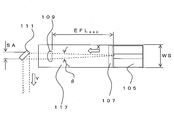
- the light (arrow X in the figure) emitted from the semiconductor laser 105 has a predetermined spread angle ( ⁇ in the figure). This spread is collimated by the lens 109 and reflected by the reflecting mirror 111 (arrow Y in the figure).
- the conventional semiconductor laser module cannot make the effective reflection width SA of the reflection mirror 111 sufficiently wide.
- the semiconductor laser 105 having a large ⁇ cannot be used.
- the installation pitch pD of the semiconductor laser 105 needs to be wider than the width WS of the semiconductor laser 105. That is, it is necessary to provide a clearance between the semiconductor lasers 105.
- the mounting efficiency of the semiconductor laser 105 makes the mounting efficiency of the semiconductor laser 105 worse. Therefore, in order to increase the mounting efficiency of the semiconductor laser 105, the light from each of the semiconductor lasers 105 is collected separately in the semiconductor laser installation rows 121a and 121b. However, if the semiconductor lasers 105 are arranged apart from each other, Thus, the effect of providing a plurality of rows of semiconductor lasers 121a and 121b cannot be sufficiently obtained.
- FIG. 10 is a conceptual diagram showing the relationship between the semiconductor laser 105 and the lens 109.
- the light X emitted from the semiconductor laser 105 has a predetermined spread angle ⁇ .
- This light X is incident on the lens 109 within a range determined by ⁇ and EFL SAC .
- the light incident in the vicinity of the end of the lens 109 in the width direction is not completely collimated and is likely to shift. This deviation is called spherical aberration. It is known that the spherical aberration is proportional to 1 / R 2 of the spherical surface of the lens 109. Therefore, in order to reduce the spherical aberration, it is necessary to increase R.
- the step pitch of the semiconductor laser installation surface 117 in each of the semiconductor laser installation rows 121a and 121b is different from the step pitch of the installation surface of the reflection mirror 111. For this reason, adjustment of each reflecting mirror 111 is difficult, and assemblability is bad.
- the present invention has been made in view of such problems, and an object of the present invention is to provide a semiconductor laser module and the like that are compact and easy to assemble.
- the first invention includes a housing, a plurality of semiconductor lasers provided in the housing, a lens for collimating each laser beam emitted from each semiconductor laser, A plurality of first reflecting mirrors for reflecting the respective laser beams, and the plurality of semiconductor lasers are stepped so as to gradually increase in height relative to the bottom of the housing.
- the semiconductor laser installation rows are arranged on the formed semiconductor laser installation rows having different heights to form a semiconductor laser installation row, and a plurality of the semiconductor laser installation rows are provided.
- the first reflection mirrors having different heights and constituting the same semiconductor laser installation row reflect light in substantially the same axial direction as viewed from above.
- Each beam group for each of the semiconductor laser installation rows is formed on different axes as viewed from above, and each beam group is provided for each of the semiconductor laser installation rows.
- the semiconductor laser module is characterized in that a second reflecting mirror to be reflected is provided, and the plurality of beam groups are collectively reflected on the same axis by each of the second reflecting mirrors.
- the first invention includes a housing, a plurality of semiconductor lasers provided in the housing, a lens for collimating each laser beam emitted from each semiconductor laser, and each of the laser beams.
- a plurality of first reflecting mirrors that reflect each other, and the plurality of semiconductor lasers are formed in a stepped shape so as to gradually increase in height relative to the bottom of the housing.
- a beam group is formed by reflecting light in substantially the same axial direction as viewed from above, and each of the beam groups in each of the semiconductor laser installation rows has different axes as viewed from above.
- the second reflection mirror includes: Even if the height of the beam group is changed, the beam group for each of the semiconductor laser installation rows is guided to the condenser lens without overlapping in the height direction. Good.
- the stepped member constituting the semiconductor laser installation surface is separate from the casing and is joined to the bottom of the casing.
- At least a pair of the semiconductor laser installation rows are arranged so that the semiconductor lasers are adjacent to each other back to back, and the emission directions of the semiconductor lasers of the pair of semiconductor laser installation rows are opposite to each other. May be.
- the beam groups for the respective semiconductor laser installation rows are formed on different axes as viewed from above, and the respective beam groups are reflected by the second reflecting mirror to be on the same axis. Since the light is focused on, the first reflecting mirrors do not interfere with each other. For this reason, even if semiconductor lasers are arranged without a gap, the effective reflection width of the first reflecting mirror can be sufficiently obtained. Therefore, even a semiconductor laser having a large ⁇ can be applied, and the distance EFL SAC can be sufficiently secured.
- each beam group reflected by the second reflecting mirror by the condenser lens can be optically coupled to the optical fiber.
- the semiconductor laser, the lens, and the first reflecting mirror are arranged on the stepped member while adjusting, and finally, A stepped member can be joined to the bottom of the housing. Further, since the position adjustment with the condenser lens can be performed by the second reflection mirror, it is not necessary to adjust the position with the second reflection mirror for each semiconductor laser, and the assemblability is good. .
- a second invention is a method for manufacturing a semiconductor laser module, wherein a stepped member formed in a stepped shape so as to gradually increase in height is used, and the stepped members are disposed at different heights from each other.
- a semiconductor laser for each surface, a semiconductor laser, a lens for collimating the laser light emitted from the semiconductor laser, and a plurality of first reflection mirrors for reflecting the laser light, and forming a semiconductor laser installation row a, a step b for fixing the plurality of semiconductor laser installation rows to the bottom of the housing, and light reflected by the first reflection mirror for each of the semiconductor laser installation rows on the bottom of the housing
- the heights of the semiconductor laser installation surfaces in the semiconductor laser installation row are different from each other, and in the semiconductor laser installation row, each of the first reflection mirrors reflects light in substantially the same axial direction as
- the beam groups for each of the semiconductor laser installation rows are configured on different axes, and in the step c, the second reflection mirror is adjusted to adjust the second reflection mirror.
- Each of the beam groups reflected by one reflecting mirror is guided to a condenser lens, and the beam group can be optically coupled to an optical fiber by the condenser lens. It is a manufacturing method.
- a method for manufacturing a semiconductor laser module comprising: a stepped member formed in a stepped shape so as to gradually increase in height; For each laser installation surface, a semiconductor laser, a lens for collimating the laser light emitted from the semiconductor laser, and a plurality of first reflection mirrors for reflecting the laser light are installed to form a semiconductor laser installation row Step a, fixing a plurality of the semiconductor laser installation rows to the bottom of the housing, and reflecting each first semiconductor laser on the bottom of the housing by each of the first reflection mirrors And c) fixing a second reflecting mirror that reflects the light in substantially the same axial direction when viewed from above, and the semiconductor laser installation rows are arranged in a plurality of rows at the bottom, In the conductor laser installation row, each of the first reflection mirrors reflects light in substantially the same axial direction when viewed from above to form a beam group, and each of the beam groups for each of the semiconductor laser installation rows Are arranged on different axes, and for at
- a compact semiconductor laser module can be easily assembled.
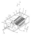
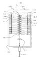
- FIG. 1 is a perspective view showing a semiconductor laser module 1.
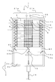
- FIG. 1 is a plan view showing a semiconductor laser module 1.
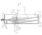
- FIG. 2 is a side view showing the semiconductor laser module 1 and shows the respective semiconductor laser installation rows 21a and 21b on the same surface.
- FIG. The figure which shows the positional relationship of the conventional semiconductor laser 105 and the reflective mirror 111.
- FIG. 1 is a perspective view showing a semiconductor laser module 1
- FIG. 2 is a plan view.
- FIG. 1 is a perspective view of the upper surface of the housing 3 and a part of the side wall 3a on the front side in the drawing, and illustration of wiring and the like is omitted.
- the semiconductor laser module 1 mainly includes a housing 3, a semiconductor laser 5, lenses 7 and 9, reflection mirrors 11, 13 a and 13 b, a condenser lens 15, an optical fiber 19, and the like.
- the housing 3 includes a side wall 3a and a bottom 3b.
- the side wall 3a stands substantially perpendicular to the bottom 3b.
- semiconductor laser installation surfaces 17 having different heights are formed stepwise so as to gradually increase in height.
- the semiconductor laser 5 is installed on each semiconductor laser installation surface 17. That is, a plurality of semiconductor lasers 5 are provided inside the housing 3.
- a lens 7 is disposed in front of the semiconductor laser 5 (in the emission direction and in the direction of arrow A in FIG. 2). Further, a lens 9 is disposed in front of the lens 9.
- the lenses 7 and 9 are arranged for each semiconductor laser 5 and are arranged on the same semiconductor laser installation surface 17. The lenses 7 and 9 collimate the light emitted from the semiconductor laser 5 in the vertical direction and the horizontal direction, respectively.
- a reflection mirror 11 as a first reflection mirror is disposed in front of the lens 9 in the emission direction of the semiconductor laser 5.
- the plurality of reflecting mirrors 11 are arranged for each semiconductor laser 5 and reflect each light collimated by the lenses 7 and 9 described above substantially vertically.
- the lenses 7 and 9 and the reflection mirror 11 for each semiconductor laser 5 can all be of the same shape.
- the reflecting mirrors 11 having different heights corresponding to the respective stages may be arranged directly on the bottom 3b.
- the semiconductor lasers 5 are arranged in a plurality of rows in a direction perpendicular to the emission direction.
- the rows of the respective semiconductor lasers 5 are referred to as semiconductor laser installation rows 21a and 21b.
- the plurality of semiconductor lasers 5 are arranged on the semiconductor laser installation surface 17 formed in a step shape so that the height is gradually increased with respect to the bottom portion 3b of the housing 3, and the semiconductor lasers 5 are arranged in a semiconductor.
- Laser installation rows 21a and 21b are configured. Further, the plurality of semiconductor laser installation rows 21a and 21b have different heights of the semiconductor laser installation surfaces 17 from each other. That is, all the semiconductor lasers 5 have different heights.
- the semiconductor lasers 5 of the pair of semiconductor laser installation rows 21a and 21b are arranged so that the semiconductor lasers 5 are adjacent to each other so that the emission directions are opposite to each other.
- the semiconductor lasers 5 are arranged in two rows substantially at the center of the housing 3, and the semiconductor lasers 5 in the respective semiconductor laser installation rows 21 a and 21 b irradiate the laser toward the outside in the width direction of the housing 3.
- the positions of the semiconductor lasers 5 in the paired semiconductor laser installation rows 21a and 21b may be the same as shown in the figure, or may be shifted (for example, , And may be arranged with a half-pitch shift as shown in FIG.
- the plurality of semiconductor lasers 5 in the semiconductor laser installation row 21a are provided side by side on the semiconductor laser installation surface 17 of each height, and each emits laser light in substantially the same direction.
- the plurality of semiconductor lasers 5 in the semiconductor laser installation row 21b are provided side by side on the respective semiconductor laser installation surfaces 17 and emit laser beams in substantially the same direction.
- the semiconductor lasers 5 in the semiconductor laser installation row 21a and the semiconductor lasers 5 in the semiconductor laser installation row 21b are disposed on the semiconductor laser installation surfaces 17 having different heights, and emit laser beams in opposite directions.
- Each of the reflection mirrors 11 constituting the same semiconductor laser installation row 21a or the same semiconductor laser installation row 21b reflects light in substantially the same axial direction as viewed from above, and the beam group 23 is formed.
- the beam groups 23 of the respective semiconductor laser installation rows 21 a and 21 b are formed on both sides in the width direction of the housing 3. That is, a beam group 23 is configured for each of the semiconductor laser installation rows 21a and 21b, and each beam group 23 is formed on different axes as viewed from above.
- Reflecting mirrors 13a and 13b which are second reflecting mirrors, that reflect the respective beam groups 23 are provided for each of the semiconductor laser installation rows 21a and 21b.
- the reflection mirror 13a reflects the beam group 23 substantially perpendicularly, and reflects the beam group 23 in the direction opposite to the emission direction of the semiconductor laser 5 (the central direction of the housing 3).
- the reflection mirror 13b further reflects the beam group 23 in the direction of the condenser lens 15 substantially vertically. That is, the plurality of beam groups 23 are reflected by the respective reflection mirrors 13a and 13b, and are grouped on substantially the same axis at substantially the center of the housing 3 when viewed from above.
- FIG. 3 is a side view of the semiconductor laser module 1, and is a conceptual diagram illustrating the semiconductor laser installation rows 21a and 21b projected on the same drawing.
- the reflection mirror 13a and the reflection mirror 13b are shown on the same plane, and the reflection point of light in each is indicated by a black circle (B in the figure).
- the reflected light from the reflection mirror 11 at each stage passes over the reflection mirror 11 at the previous stage without reaching the reflection mirror 11 at the previous stage, and reaches the reflection mirror 13a. Therefore, the reflection mirror 13a and the reflection mirror 13b collectively reflect the beam groups 23 having different heights.
- the height of the beam group 23 is different for each of the semiconductor laser installation rows 21a and 21b. For this reason, the reflection mirror 13 a and the reflection mirror 13 b that reflect the beam group 23 at substantially the center have different heights so as not to interfere with the respective beam groups 23.
- a condenser lens 15 is fixed to the bottom 3 b of the housing 3 in a direction perpendicular to the emitting direction of the semiconductor laser 5.
- the condensing lens 15 condenses the plurality of beam groups 23 reflected by the respective reflecting mirrors 13b.
- an optical fiber 19 is provided on the back side of the condenser lens 15 so as to penetrate the side wall 3 a of the housing 3.
- the beam group 23 collected by the condenser lens 15 is optically coupled to the optical fiber 19.
- the arrangement and number of the semiconductor laser 5, each reflection mirror, the lenses 7 and 9, and the condenser lens 15 are not limited to the illustrated example.
- a plurality of independent condensing lenses 15 that condense each of the horizontal direction and the vertical direction may be arranged.
- the number of semiconductor laser installation rows may be three or more.
- the semiconductor lasers 5 in the semiconductor laser installation rows 21a and 21b are arranged so as to be adjacent to each other back to back in the approximate center of the housing 3, but they may be reversed.
- the wiring 27 for driving the semiconductor laser 5 can be shortened and the terminals 25 can be arranged close to each other.
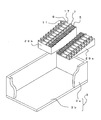
- FIG. 4 is an exploded perspective view of the semiconductor laser module 1.
- stepped members 29a and 29b formed in a stepped shape so as to gradually increase in height are used.
- the stepped members 29a and 29b constituting the housing 3 and the semiconductor laser installation surface 17 are separate bodies.
- the stepped member 29a and the stepped member 29b have different heights.
- the lowest semiconductor laser installation surface 17 of the stepped member 29b is higher than the height of the highest semiconductor laser installation surface 17 of the stepped member 29a.
- the semiconductor laser 5, the lenses 7 and 9, and the reflection mirror 11 are installed for each semiconductor laser installation surface 17 of the stepped members 29a and 29b having different heights, and the semiconductor laser installation rows 21a and 21b are arranged.
- the semiconductor laser 5, the lenses 7, 9, and the reflecting mirror 11 can be positioned on the respective stepped members 29a, 29b.
- the respective step-like members 29 a and 29 b are joined and fixed on the bottom 3 b of the housing 3.
- the reflection mirrors 13a and 13b are fixed to the bottom 3b of the housing 3 for each of the semiconductor laser installation rows 21a and 21b.
- the optical axis can be easily adjusted by adjusting the reflection mirrors 13a and 13b for each of the semiconductor laser installation rows 21a and 21b. For this reason, it is possible to guide each beam group 23 reflected by each reflecting mirror 11 to the condenser lens 15 and to optically couple the beam group 23 to the optical fiber 19 by the condenser lens 15.
- the step-like members 29a and 29b having different heights are used, but the present invention is not limited to this.
- a plurality of the same step-like members 29a may be used, and a spacer 31 may be joined to the lower surface of some of the step-like members 29a.
- the thickness of the spacer 31 is set so that the height of the semiconductor installation row is approximately the same as when the stepped member 29b is used. By doing so, a plurality of semiconductor laser installation rows can be formed by one type of stepped member 29a.
- a compact semiconductor laser module 1 can be obtained.
- the respective beam groups 23 are reflected on different axes as viewed from above, and the respective beam groups 23 are reflected on the same axis by the reflecting mirrors 13a and 13b. For this reason, the effective reflection width of the reflection mirror 11 can be brought close to the width of the semiconductor laser 5. As a result, the semiconductor laser 5 having a large ⁇ can be applied, and the distance between the semiconductor laser 5 and the lens 9 can be increased, so that spherical aberration in the lens 9 can be suppressed.
- the semiconductor lasers 5 in the semiconductor laser installation rows 21a and 21b are arranged so as to be back to back. For this reason, the arrangement of the wiring 27 of the semiconductor laser 5 is easy, and the wiring 27 can be shortened.
- the stepped members 29a and 29b may be configured integrally. That is, you may form the bottom part 3b in step shape.
- FIG. 6 is a perspective view showing a semiconductor laser module 1a according to the second embodiment.
- components having the same functions as those of the semiconductor laser module 1 are denoted by the same reference numerals as those in FIGS. 1 to 5, and redundant descriptions are omitted.
- the semiconductor laser module 1a has substantially the same configuration as the semiconductor laser module 1, but differs in that the reflection mirrors 33 and 34 are arranged.
- the heights of the respective semiconductor laser installation rows 21a and 21b are the same. That is, the same step-like member 29a can be used.
- the reflection mirrors 33 and 34 are arranged between the reflection mirrors 13a and 13b for one semiconductor laser installation row.
- the reflection mirrors 33 and 34 reflect light incident from the side once upward substantially perpendicularly, and further reflect light substantially perpendicularly in the same direction as the incident direction. That is, the reflection mirrors 33 and 34 can change the height of the incident light.
- the reflection mirrors 33 and 34 are combined to form a second reflection mirror.
- FIG. 7 is a diagram showing an optical path when viewed from the light coupling direction (optical fiber) side (illustration of a semiconductor laser or the like is omitted).
- the reflection points of light on the reflection mirrors 13a, 13b, 33, and 34 are indicated by black circles.
- the left half of the figure shows the beam group 23 from the semiconductor laser installation row 21a, and the right half of the figure shows the beam group 23 from the semiconductor laser installation row 21b.
- the respective beam groups 23 reflected by the reflecting mirror 11 in the semiconductor laser installation rows 21a and 21b have the same height.
- reflection mirrors 33 and 34 are arranged on the optical path of one of the semiconductor laser installation rows 21a. That is, the optical path height of the beam group 23 is changed by the reflection mirrors 33 and 34.
- the optical path is displaced upward by the reflecting mirrors 33 and 34 so that the beam group 23 of the semiconductor laser installation row 21a does not overlap the beam group 23 of the semiconductor laser installation row 21b.
- each beam group 23 can be reflected by the reflecting mirrors 13b having different heights and incident on the condenser lens 15.
- the same effect as that of the first embodiment can be obtained. Further, since the semiconductor laser installation surfaces 17 of the semiconductor laser installation rows 21a and 21b can be made the same, the same stepped member 29a can be used.
- the reflection mirrors 33 and 34 are disposed between the reflection mirrors 13a and 13b, but the present invention is not limited to this.
- the reflection mirrors 33 and 34 may be arranged at the position of the reflection mirror 13a, and the change in the optical path height direction and the change in the traveling direction of the optical path may be simultaneously performed by an integral reflection mirror. Further, a plurality of reflection mirrors may be used.
- the reflecting mirrors 33 and 34 may be omitted by arranging the reflecting mirror 13a slightly upward and making the reflecting mirror 13b substantially parallel to the bottom 3b.
- the second reflection mirrors change the height of the beam group 23 with respect to at least one of the semiconductor laser installation rows. , 21b are guided to the condenser lens 15 without overlapping in the height direction.
Landscapes
- Physics & Mathematics (AREA)
- General Physics & Mathematics (AREA)
- Optics & Photonics (AREA)
- Condensed Matter Physics & Semiconductors (AREA)
- Electromagnetism (AREA)
- Optical Couplings Of Light Guides (AREA)
- Semiconductor Lasers (AREA)
Abstract
Des lasers à semi-conducteur 5 sont disposés en une pluralité de colonnes. Les colonnes des lasers à semi-conducteur 5 respectifs comprennent des colonnes installées de lasers à semi-conducteur 21a, 21b. Des miroirs réfléchissants 11 dans les colonnes installées de lasers à semi-conducteur 21a, 21b respectives réfléchissent la lumière sensiblement dans la même direction axiale en vue de dessus, et constituent des groupes de faisceaux 23. Les groupes de faisceaux 23 des colonnes installées de lasers à semi-conducteur 21a, 21b respectives sont formés sur les deux côtés dans le sens de la largeur d'un boîtier 3. À savoir, les groupes de faisceaux 23 sont conçus pour chacune des colonnes installés de lasers à semi-conducteur 21a, 21b, et les groupes de faisceaux 23 respectifs sont formés sur des axes mutuellement différents en vue de dessus.
Priority Applications (3)
| Application Number | Priority Date | Filing Date | Title |
|---|---|---|---|
| CN201780006201.4A CN108463929B (zh) | 2016-01-14 | 2017-01-13 | 半导体激光器模块、半导体激光器模块的制造方法 |
| JP2017561188A JP6935337B2 (ja) | 2016-01-14 | 2017-01-13 | 半導体レーザモジュール、半導体レーザモジュール製造方法 |
| US16/034,762 US10361532B2 (en) | 2016-01-14 | 2018-07-13 | Semiconductor laser module and semiconductor laser module manufacturing method |
Applications Claiming Priority (2)
| Application Number | Priority Date | Filing Date | Title |
|---|---|---|---|
| JP2016-004998 | 2016-01-14 | ||
| JP2016004998 | 2016-01-14 |
Related Child Applications (1)
| Application Number | Title | Priority Date | Filing Date |
|---|---|---|---|
| US16/034,762 Continuation US10361532B2 (en) | 2016-01-14 | 2018-07-13 | Semiconductor laser module and semiconductor laser module manufacturing method |
Publications (1)
| Publication Number | Publication Date |
|---|---|
| WO2017122792A1 true WO2017122792A1 (fr) | 2017-07-20 |
Family
ID=59311982
Family Applications (1)
| Application Number | Title | Priority Date | Filing Date |
|---|---|---|---|
| PCT/JP2017/001058 Ceased WO2017122792A1 (fr) | 2016-01-14 | 2017-01-13 | Module de laser à semi-conducteur et procédé de fabrication de module de laser à semi-conducteur |
Country Status (4)
| Country | Link |
|---|---|
| US (1) | US10361532B2 (fr) |
| JP (1) | JP6935337B2 (fr) |
| CN (1) | CN108463929B (fr) |
| WO (1) | WO2017122792A1 (fr) |
Cited By (6)
| Publication number | Priority date | Publication date | Assignee | Title |
|---|---|---|---|---|
| CN109586163A (zh) * | 2018-07-04 | 2019-04-05 | 深圳朗光科技有限公司 | 多单管大功率半导体激光器封装结构及激光器 |
| WO2019176181A1 (fr) * | 2018-03-13 | 2019-09-19 | 株式会社フジクラ | Module laser |
| WO2021039386A1 (fr) * | 2019-08-23 | 2021-03-04 | 古河電気工業株式会社 | Dispositif laser |
| JP2022030621A (ja) * | 2020-08-07 | 2022-02-18 | パナソニックIpマネジメント株式会社 | レーザ装置およびレーザ装置の光軸調整方法 |
| JP2022071758A (ja) * | 2020-10-28 | 2022-05-16 | 矢崎総業株式会社 | 半導体レーザモジュール |
| WO2023189268A1 (fr) * | 2022-03-31 | 2023-10-05 | 古河電気工業株式会社 | Dispositif électroluminescent et dispositif de source lumineuse |
Families Citing this family (12)
| Publication number | Priority date | Publication date | Assignee | Title |
|---|---|---|---|---|
| EP3267536A1 (fr) * | 2016-07-05 | 2018-01-10 | Cobolt AB | Système laser à longueurs d'ondes multiples |
| US11025031B2 (en) | 2016-11-29 | 2021-06-01 | Leonardo Electronics Us Inc. | Dual junction fiber-coupled laser diode and related methods |
| US11406004B2 (en) | 2018-08-13 | 2022-08-02 | Leonardo Electronics Us Inc. | Use of metal-core printed circuit board (PCB) for generation of ultra-narrow, high-current pulse driver |
| US11056854B2 (en) * | 2018-08-14 | 2021-07-06 | Leonardo Electronics Us Inc. | Laser assembly and related methods |
| US11824323B1 (en) * | 2018-12-06 | 2023-11-21 | Nlight, Inc. | Diode laser package for bidirectionally emitting semiconductor laser devices |
| US11296481B2 (en) | 2019-01-09 | 2022-04-05 | Leonardo Electronics Us Inc. | Divergence reshaping array |
| US11752571B1 (en) | 2019-06-07 | 2023-09-12 | Leonardo Electronics Us Inc. | Coherent beam coupler |
| EP3792683A1 (fr) | 2019-09-16 | 2021-03-17 | Leonardo Electronics US Inc. | Homogénéisateur hexagonal à intensité d'entrée asymétrique |
| CN112436382A (zh) * | 2021-01-26 | 2021-03-02 | 深圳市星汉激光科技股份有限公司 | 一种高功率半导体激光器 |
| CN112600074B (zh) * | 2021-03-05 | 2021-06-01 | 深圳市星汉激光科技股份有限公司 | 一种小体积高功率半导体激光器 |
| JP7723266B2 (ja) * | 2021-10-19 | 2025-08-14 | 日亜化学工業株式会社 | 光源装置 |
| CN116526301B (zh) * | 2023-05-10 | 2026-03-17 | 江苏长光时空光电技术有限公司 | 一种面发射激光半导体列阵芯片及其制作方法 |
Citations (6)
| Publication number | Priority date | Publication date | Assignee | Title |
|---|---|---|---|---|
| JP2009128689A (ja) * | 2007-11-26 | 2009-06-11 | Ricoh Co Ltd | 投射型表示装置 |
| US20090323752A1 (en) * | 2008-06-26 | 2009-12-31 | Vadim Chuyanov | High brightness laser diode module |
| US20120002395A1 (en) * | 2010-06-30 | 2012-01-05 | Jds Uniphase Corporation | Beam combining light source |
| JP2013152385A (ja) * | 2012-01-26 | 2013-08-08 | Jvc Kenwood Corp | 投射型表示装置 |
| WO2016203998A1 (fr) * | 2015-06-19 | 2016-12-22 | 株式会社アマダミヤチ | Unité laser et dispositif laser |
| WO2017026358A1 (fr) * | 2015-08-07 | 2017-02-16 | カナレ電気株式会社 | Source de lumière laser à semi-conducteur de type à couplage de faisceaux à verrouillage en longueur d'onde |
Family Cites Families (7)
| Publication number | Priority date | Publication date | Assignee | Title |
|---|---|---|---|---|
| JP2000114655A (ja) * | 1998-09-30 | 2000-04-21 | Toshiba Corp | サブマウントミラー方式面型レーザ |
| CN100460927C (zh) * | 2004-04-13 | 2009-02-11 | 浜松光子学株式会社 | 聚光装置以及聚光反射镜 |
| US8432945B2 (en) | 2010-09-30 | 2013-04-30 | Victor Faybishenko | Laser diode combiner modules |
| JP5730814B2 (ja) * | 2012-05-08 | 2015-06-10 | 古河電気工業株式会社 | 半導体レーザモジュール |
| JP5920254B2 (ja) * | 2013-03-13 | 2016-05-18 | ウシオ電機株式会社 | 半導体レーザ装置 |
| US20170222401A1 (en) * | 2015-05-13 | 2017-08-03 | Trumpf Laser Gmbh | Dense wavelength beam combining with variable feedback control |
| JP7272959B2 (ja) * | 2017-01-10 | 2023-05-12 | エヌライト,インコーポレーテッド | 最適化されたビーム寸法を有するダイオードを使用したファイバ結合式ダイオードレーザにおけるパワーおよび輝度スケーリング |
-
2017
- 2017-01-13 WO PCT/JP2017/001058 patent/WO2017122792A1/fr not_active Ceased
- 2017-01-13 JP JP2017561188A patent/JP6935337B2/ja active Active
- 2017-01-13 CN CN201780006201.4A patent/CN108463929B/zh active Active
-
2018
- 2018-07-13 US US16/034,762 patent/US10361532B2/en active Active
Patent Citations (6)
| Publication number | Priority date | Publication date | Assignee | Title |
|---|---|---|---|---|
| JP2009128689A (ja) * | 2007-11-26 | 2009-06-11 | Ricoh Co Ltd | 投射型表示装置 |
| US20090323752A1 (en) * | 2008-06-26 | 2009-12-31 | Vadim Chuyanov | High brightness laser diode module |
| US20120002395A1 (en) * | 2010-06-30 | 2012-01-05 | Jds Uniphase Corporation | Beam combining light source |
| JP2013152385A (ja) * | 2012-01-26 | 2013-08-08 | Jvc Kenwood Corp | 投射型表示装置 |
| WO2016203998A1 (fr) * | 2015-06-19 | 2016-12-22 | 株式会社アマダミヤチ | Unité laser et dispositif laser |
| WO2017026358A1 (fr) * | 2015-08-07 | 2017-02-16 | カナレ電気株式会社 | Source de lumière laser à semi-conducteur de type à couplage de faisceaux à verrouillage en longueur d'onde |
Cited By (15)
| Publication number | Priority date | Publication date | Assignee | Title |
|---|---|---|---|---|
| US11675144B2 (en) | 2018-03-13 | 2023-06-13 | Fujikura Ltd. | Laser module |
| WO2019176181A1 (fr) * | 2018-03-13 | 2019-09-19 | 株式会社フジクラ | Module laser |
| JP2019161005A (ja) * | 2018-03-13 | 2019-09-19 | 株式会社フジクラ | レーザモジュール |
| CN109586163B (zh) * | 2018-07-04 | 2020-11-03 | 深圳朗光科技有限公司 | 多单管大功率半导体激光器封装结构及激光器 |
| CN109586163A (zh) * | 2018-07-04 | 2019-04-05 | 深圳朗光科技有限公司 | 多单管大功率半导体激光器封装结构及激光器 |
| WO2021039386A1 (fr) * | 2019-08-23 | 2021-03-04 | 古河電気工業株式会社 | Dispositif laser |
| JPWO2021039386A1 (fr) * | 2019-08-23 | 2021-03-04 | ||
| JP7558955B2 (ja) | 2019-08-23 | 2024-10-01 | 古河電気工業株式会社 | レーザ装置 |
| JP2022030621A (ja) * | 2020-08-07 | 2022-02-18 | パナソニックIpマネジメント株式会社 | レーザ装置およびレーザ装置の光軸調整方法 |
| JP7515075B2 (ja) | 2020-08-07 | 2024-07-12 | パナソニックIpマネジメント株式会社 | レーザ装置およびレーザ装置の光軸調整方法 |
| JP7505962B2 (ja) | 2020-10-28 | 2024-06-25 | 矢崎総業株式会社 | 半導体レーザモジュール |
| JP2022071758A (ja) * | 2020-10-28 | 2022-05-16 | 矢崎総業株式会社 | 半導体レーザモジュール |
| WO2023189268A1 (fr) * | 2022-03-31 | 2023-10-05 | 古河電気工業株式会社 | Dispositif électroluminescent et dispositif de source lumineuse |
| JP2023149503A (ja) * | 2022-03-31 | 2023-10-13 | 古河電気工業株式会社 | 発光装置および光源装置 |
| JP7727587B2 (ja) | 2022-03-31 | 2025-08-21 | 古河電気工業株式会社 | 発光装置および光源装置 |
Also Published As
| Publication number | Publication date |
|---|---|
| JPWO2017122792A1 (ja) | 2018-11-01 |
| US20180335582A1 (en) | 2018-11-22 |
| CN108463929B (zh) | 2020-10-30 |
| CN108463929A (zh) | 2018-08-28 |
| JP6935337B2 (ja) | 2021-09-15 |
| US10361532B2 (en) | 2019-07-23 |
Similar Documents
| Publication | Publication Date | Title |
|---|---|---|
| JP6935337B2 (ja) | 半導体レーザモジュール、半導体レーザモジュール製造方法 | |
| US7502176B2 (en) | Combined laser source having deflection member | |
| JP4980329B2 (ja) | 少なくとも1つの高出力ダイオードレーザを含む高出力レーザダイオードアレイ、及びそれを含むレーザ光源 | |
| JP6244721B2 (ja) | 波長多重伝送装置の製造方法 | |
| CN104868361B (zh) | 光源系统与激光光源 | |
| US10838217B2 (en) | Laser diode collimator and a pattern projecting device using same | |
| US20050232628A1 (en) | Device for the optical beam transformation of a linear arrangement of several light sources | |
| JP2008501144A (ja) | 光ファイバへの2次元のレーザアレイスタックの出力の最適な整合 | |
| KR101905102B1 (ko) | 광섬유와 결합된 복층 단차 배열 구조의 레이져 다이오드 모듈 | |
| WO2013150864A1 (fr) | Dispositif optique de laser à semi-conducteur | |
| JP2011076092A (ja) | レーザビームを形成するための装置 | |
| KR101033759B1 (ko) | 반도체 레이저 장치 | |
| CN112673294A (zh) | 复用光学系统 | |
| KR102905243B1 (ko) | 섬유 결합 다이오드 레이저 모듈 및 그 조립 방법 | |
| CN111801856B (zh) | 激光模块 | |
| CN103180774B (zh) | 用于在工作平面内产生线状的强度分布的激光设备 | |
| JP7561181B2 (ja) | 半導体レーザ装置 | |
| JP2025038147A (ja) | 発光モジュール | |
| CN120315076B (zh) | 光学系统以及激光雷达 | |
| JP7331902B2 (ja) | 光源装置及び投影装置 | |
| CN115903348B (zh) | 光源装置和投影装置 | |
| KR102165519B1 (ko) | 빔 적층 방법이 개선된 레이저 다이오드 모듈 | |
| CN120914598B (zh) | 半导体激光模块及其制备方法 | |
| CN222441104U (zh) | 一种阶梯式半导体激光输出装置 | |
| JP2025147506A (ja) | 照明装置 |
Legal Events
| Date | Code | Title | Description |
|---|---|---|---|
| 121 | Ep: the epo has been informed by wipo that ep was designated in this application |
Ref document number: 17738544 Country of ref document: EP Kind code of ref document: A1 |
|
| ENP | Entry into the national phase |
Ref document number: 2017561188 Country of ref document: JP Kind code of ref document: A |
|
| NENP | Non-entry into the national phase |
Ref country code: DE |
|
| 122 | Ep: pct application non-entry in european phase |
Ref document number: 17738544 Country of ref document: EP Kind code of ref document: A1 |