WO2017122820A1 - Précurseur de frp, plaque stratifiée, stratifié à revêtement métallique, carte de circuit imprimé, boîtier de semi-conducteur et procédé de production associé - Google Patents
Précurseur de frp, plaque stratifiée, stratifié à revêtement métallique, carte de circuit imprimé, boîtier de semi-conducteur et procédé de production associé Download PDFInfo
- Publication number
- WO2017122820A1 WO2017122820A1 PCT/JP2017/001134 JP2017001134W WO2017122820A1 WO 2017122820 A1 WO2017122820 A1 WO 2017122820A1 JP 2017001134 W JP2017001134 W JP 2017001134W WO 2017122820 A1 WO2017122820 A1 WO 2017122820A1
- Authority
- WO
- WIPO (PCT)
- Prior art keywords
- metal
- clad laminate
- frp
- less
- frp precursor
- Prior art date
- Legal status (The legal status is an assumption and is not a legal conclusion. Google has not performed a legal analysis and makes no representation as to the accuracy of the status listed.)
- Ceased
Links
Images

Classifications
-
- B—PERFORMING OPERATIONS; TRANSPORTING
- B32—LAYERED PRODUCTS
- B32B—LAYERED PRODUCTS, i.e. PRODUCTS BUILT-UP OF STRATA OF FLAT OR NON-FLAT, e.g. CELLULAR OR HONEYCOMB, FORM
- B32B5/00—Layered products characterised by the non- homogeneity or physical structure, i.e. comprising a fibrous, filamentary, particulate or foam layer; Layered products characterised by having a layer differing constitutionally or physically in different parts
- B32B5/02—Layered products characterised by the non- homogeneity or physical structure, i.e. comprising a fibrous, filamentary, particulate or foam layer; Layered products characterised by having a layer differing constitutionally or physically in different parts characterised by structural features of a fibrous or filamentary layer
- B32B5/022—Non-woven fabric
-
- B—PERFORMING OPERATIONS; TRANSPORTING
- B32—LAYERED PRODUCTS
- B32B—LAYERED PRODUCTS, i.e. PRODUCTS BUILT-UP OF STRATA OF FLAT OR NON-FLAT, e.g. CELLULAR OR HONEYCOMB, FORM
- B32B15/00—Layered products comprising a layer of metal
- B32B15/04—Layered products comprising a layer of metal comprising metal as the main or only constituent of a layer, which is next to another layer of the same or of a different material
- B32B15/08—Layered products comprising a layer of metal comprising metal as the main or only constituent of a layer, which is next to another layer of the same or of a different material of synthetic resin
-
- B—PERFORMING OPERATIONS; TRANSPORTING
- B29—WORKING OF PLASTICS; WORKING OF SUBSTANCES IN A PLASTIC STATE IN GENERAL
- B29B—PREPARATION OR PRETREATMENT OF THE MATERIAL TO BE SHAPED; MAKING GRANULES OR PREFORMS; RECOVERY OF PLASTICS OR OTHER CONSTITUENTS OF WASTE MATERIAL CONTAINING PLASTICS
- B29B11/00—Making preforms
- B29B11/14—Making preforms characterised by structure or composition
- B29B11/16—Making preforms characterised by structure or composition comprising fillers or reinforcement
-
- B—PERFORMING OPERATIONS; TRANSPORTING
- B29—WORKING OF PLASTICS; WORKING OF SUBSTANCES IN A PLASTIC STATE IN GENERAL
- B29C—SHAPING OR JOINING OF PLASTICS; SHAPING OF MATERIAL IN A PLASTIC STATE, NOT OTHERWISE PROVIDED FOR; AFTER-TREATMENT OF THE SHAPED PRODUCTS, e.g. REPAIRING
- B29C65/00—Joining or sealing of preformed parts, e.g. welding of plastics materials; Apparatus therefor
- B29C65/02—Joining or sealing of preformed parts, e.g. welding of plastics materials; Apparatus therefor by heating, with or without pressure
-
- B—PERFORMING OPERATIONS; TRANSPORTING
- B29—WORKING OF PLASTICS; WORKING OF SUBSTANCES IN A PLASTIC STATE IN GENERAL
- B29C—SHAPING OR JOINING OF PLASTICS; SHAPING OF MATERIAL IN A PLASTIC STATE, NOT OTHERWISE PROVIDED FOR; AFTER-TREATMENT OF THE SHAPED PRODUCTS, e.g. REPAIRING
- B29C66/00—General aspects of processes or apparatus for joining preformed parts
- B29C66/40—General aspects of joining substantially flat articles, e.g. plates, sheets or web-like materials; Making flat seams in tubular or hollow articles; Joining single elements to substantially flat surfaces
- B29C66/41—Joining substantially flat articles ; Making flat seams in tubular or hollow articles
- B29C66/45—Joining of substantially the whole surface of the articles
-
- B—PERFORMING OPERATIONS; TRANSPORTING
- B29—WORKING OF PLASTICS; WORKING OF SUBSTANCES IN A PLASTIC STATE IN GENERAL
- B29C—SHAPING OR JOINING OF PLASTICS; SHAPING OF MATERIAL IN A PLASTIC STATE, NOT OTHERWISE PROVIDED FOR; AFTER-TREATMENT OF THE SHAPED PRODUCTS, e.g. REPAIRING
- B29C66/00—General aspects of processes or apparatus for joining preformed parts
- B29C66/70—General aspects of processes or apparatus for joining preformed parts characterised by the composition, physical properties or the structure of the material of the parts to be joined; Joining with non-plastics material
- B29C66/74—Joining plastics material to non-plastics material
- B29C66/742—Joining plastics material to non-plastics material to metals or their alloys
- B29C66/7428—Transition metals or their alloys
- B29C66/74281—Copper or alloys of copper
-
- B—PERFORMING OPERATIONS; TRANSPORTING
- B32—LAYERED PRODUCTS
- B32B—LAYERED PRODUCTS, i.e. PRODUCTS BUILT-UP OF STRATA OF FLAT OR NON-FLAT, e.g. CELLULAR OR HONEYCOMB, FORM
- B32B15/00—Layered products comprising a layer of metal
- B32B15/14—Layered products comprising a layer of metal next to a fibrous or filamentary layer
-
- B—PERFORMING OPERATIONS; TRANSPORTING
- B32—LAYERED PRODUCTS
- B32B—LAYERED PRODUCTS, i.e. PRODUCTS BUILT-UP OF STRATA OF FLAT OR NON-FLAT, e.g. CELLULAR OR HONEYCOMB, FORM
- B32B15/00—Layered products comprising a layer of metal
- B32B15/18—Layered products comprising a layer of metal comprising iron or steel
-
- B—PERFORMING OPERATIONS; TRANSPORTING
- B32—LAYERED PRODUCTS
- B32B—LAYERED PRODUCTS, i.e. PRODUCTS BUILT-UP OF STRATA OF FLAT OR NON-FLAT, e.g. CELLULAR OR HONEYCOMB, FORM
- B32B15/00—Layered products comprising a layer of metal
- B32B15/20—Layered products comprising a layer of metal comprising aluminium or copper
-
- B—PERFORMING OPERATIONS; TRANSPORTING
- B32—LAYERED PRODUCTS
- B32B—LAYERED PRODUCTS, i.e. PRODUCTS BUILT-UP OF STRATA OF FLAT OR NON-FLAT, e.g. CELLULAR OR HONEYCOMB, FORM
- B32B19/00—Layered products comprising a layer of natural mineral fibres or particles, e.g. asbestos, mica
- B32B19/04—Layered products comprising a layer of natural mineral fibres or particles, e.g. asbestos, mica next to another layer of the same or of a different material
-
- B—PERFORMING OPERATIONS; TRANSPORTING
- B32—LAYERED PRODUCTS
- B32B—LAYERED PRODUCTS, i.e. PRODUCTS BUILT-UP OF STRATA OF FLAT OR NON-FLAT, e.g. CELLULAR OR HONEYCOMB, FORM
- B32B19/00—Layered products comprising a layer of natural mineral fibres or particles, e.g. asbestos, mica
- B32B19/04—Layered products comprising a layer of natural mineral fibres or particles, e.g. asbestos, mica next to another layer of the same or of a different material
- B32B19/041—Layered products comprising a layer of natural mineral fibres or particles, e.g. asbestos, mica next to another layer of the same or of a different material of metal
-
- B—PERFORMING OPERATIONS; TRANSPORTING
- B32—LAYERED PRODUCTS
- B32B—LAYERED PRODUCTS, i.e. PRODUCTS BUILT-UP OF STRATA OF FLAT OR NON-FLAT, e.g. CELLULAR OR HONEYCOMB, FORM
- B32B19/00—Layered products comprising a layer of natural mineral fibres or particles, e.g. asbestos, mica
- B32B19/06—Layered products comprising a layer of natural mineral fibres or particles, e.g. asbestos, mica next to a fibrous or filamentary layer
-
- B—PERFORMING OPERATIONS; TRANSPORTING
- B32—LAYERED PRODUCTS
- B32B—LAYERED PRODUCTS, i.e. PRODUCTS BUILT-UP OF STRATA OF FLAT OR NON-FLAT, e.g. CELLULAR OR HONEYCOMB, FORM
- B32B19/00—Layered products comprising a layer of natural mineral fibres or particles, e.g. asbestos, mica
- B32B19/08—Layered products comprising a layer of natural mineral fibres or particles, e.g. asbestos, mica comprising asbestos
-
- B—PERFORMING OPERATIONS; TRANSPORTING
- B32—LAYERED PRODUCTS
- B32B—LAYERED PRODUCTS, i.e. PRODUCTS BUILT-UP OF STRATA OF FLAT OR NON-FLAT, e.g. CELLULAR OR HONEYCOMB, FORM
- B32B5/00—Layered products characterised by the non- homogeneity or physical structure, i.e. comprising a fibrous, filamentary, particulate or foam layer; Layered products characterised by having a layer differing constitutionally or physically in different parts
- B32B5/02—Layered products characterised by the non- homogeneity or physical structure, i.e. comprising a fibrous, filamentary, particulate or foam layer; Layered products characterised by having a layer differing constitutionally or physically in different parts characterised by structural features of a fibrous or filamentary layer
- B32B5/024—Woven fabric
-
- B—PERFORMING OPERATIONS; TRANSPORTING
- B32—LAYERED PRODUCTS
- B32B—LAYERED PRODUCTS, i.e. PRODUCTS BUILT-UP OF STRATA OF FLAT OR NON-FLAT, e.g. CELLULAR OR HONEYCOMB, FORM
- B32B5/00—Layered products characterised by the non- homogeneity or physical structure, i.e. comprising a fibrous, filamentary, particulate or foam layer; Layered products characterised by having a layer differing constitutionally or physically in different parts
- B32B5/02—Layered products characterised by the non- homogeneity or physical structure, i.e. comprising a fibrous, filamentary, particulate or foam layer; Layered products characterised by having a layer differing constitutionally or physically in different parts characterised by structural features of a fibrous or filamentary layer
- B32B5/08—Layered products characterised by the non- homogeneity or physical structure, i.e. comprising a fibrous, filamentary, particulate or foam layer; Layered products characterised by having a layer differing constitutionally or physically in different parts characterised by structural features of a fibrous or filamentary layer the fibres or filaments of a layer being of different substances, e.g. conjugate fibres, mixture of different fibres
-
- B—PERFORMING OPERATIONS; TRANSPORTING
- B32—LAYERED PRODUCTS
- B32B—LAYERED PRODUCTS, i.e. PRODUCTS BUILT-UP OF STRATA OF FLAT OR NON-FLAT, e.g. CELLULAR OR HONEYCOMB, FORM
- B32B5/00—Layered products characterised by the non- homogeneity or physical structure, i.e. comprising a fibrous, filamentary, particulate or foam layer; Layered products characterised by having a layer differing constitutionally or physically in different parts
- B32B5/22—Layered products characterised by the non- homogeneity or physical structure, i.e. comprising a fibrous, filamentary, particulate or foam layer; Layered products characterised by having a layer differing constitutionally or physically in different parts characterised by the presence of two or more layers which are next to each other and are fibrous, filamentary, formed of particles or foamed
- B32B5/24—Layered products characterised by the non- homogeneity or physical structure, i.e. comprising a fibrous, filamentary, particulate or foam layer; Layered products characterised by having a layer differing constitutionally or physically in different parts characterised by the presence of two or more layers which are next to each other and are fibrous, filamentary, formed of particles or foamed one layer being a fibrous or filamentary layer
- B32B5/26—Layered products characterised by the non- homogeneity or physical structure, i.e. comprising a fibrous, filamentary, particulate or foam layer; Layered products characterised by having a layer differing constitutionally or physically in different parts characterised by the presence of two or more layers which are next to each other and are fibrous, filamentary, formed of particles or foamed one layer being a fibrous or filamentary layer another layer next to it also being fibrous or filamentary
-
- C—CHEMISTRY; METALLURGY
- C08—ORGANIC MACROMOLECULAR COMPOUNDS; THEIR PREPARATION OR CHEMICAL WORKING-UP; COMPOSITIONS BASED THEREON
- C08J—WORKING-UP; GENERAL PROCESSES OF COMPOUNDING; AFTER-TREATMENT NOT COVERED BY SUBCLASSES C08B, C08C, C08F, C08G or C08H
- C08J5/00—Manufacture of articles or shaped materials containing macromolecular substances
- C08J5/24—Impregnating materials with prepolymers which can be polymerised in situ, e.g. manufacture of prepregs
- C08J5/241—Impregnating materials with prepolymers which can be polymerised in situ, e.g. manufacture of prepregs using inorganic fibres
- C08J5/244—Impregnating materials with prepolymers which can be polymerised in situ, e.g. manufacture of prepregs using inorganic fibres using glass fibres
-
- H—ELECTRICITY
- H05—ELECTRIC TECHNIQUES NOT OTHERWISE PROVIDED FOR
- H05K—PRINTED CIRCUITS; CASINGS OR CONSTRUCTIONAL DETAILS OF ELECTRIC APPARATUS; MANUFACTURE OF ASSEMBLAGES OF ELECTRICAL COMPONENTS
- H05K1/00—Printed circuits
- H05K1/02—Details
- H05K1/03—Use of materials for the substrate
- H05K1/0313—Organic insulating material
- H05K1/0353—Organic insulating material consisting of two or more materials, e.g. two or more polymers, polymer + filler, + reinforcement
- H05K1/036—Multilayers with layers of different types
-
- H—ELECTRICITY
- H05—ELECTRIC TECHNIQUES NOT OTHERWISE PROVIDED FOR
- H05K—PRINTED CIRCUITS; CASINGS OR CONSTRUCTIONAL DETAILS OF ELECTRIC APPARATUS; MANUFACTURE OF ASSEMBLAGES OF ELECTRICAL COMPONENTS
- H05K1/00—Printed circuits
- H05K1/02—Details
- H05K1/03—Use of materials for the substrate
- H05K1/0313—Organic insulating material
- H05K1/0353—Organic insulating material consisting of two or more materials, e.g. two or more polymers, polymer + filler, + reinforcement
- H05K1/0366—Organic insulating material consisting of two or more materials, e.g. two or more polymers, polymer + filler, + reinforcement reinforced, e.g. by fibres, fabrics
-
- H—ELECTRICITY
- H05—ELECTRIC TECHNIQUES NOT OTHERWISE PROVIDED FOR
- H05K—PRINTED CIRCUITS; CASINGS OR CONSTRUCTIONAL DETAILS OF ELECTRIC APPARATUS; MANUFACTURE OF ASSEMBLAGES OF ELECTRICAL COMPONENTS
- H05K1/00—Printed circuits
- H05K1/02—Details
- H05K1/03—Use of materials for the substrate
- H05K1/05—Insulated conductive substrates, e.g. insulated metal substrate
- H05K1/056—Insulated conductive substrates, e.g. insulated metal substrate the metal substrate being covered by an organic insulating layer
-
- H—ELECTRICITY
- H05—ELECTRIC TECHNIQUES NOT OTHERWISE PROVIDED FOR
- H05K—PRINTED CIRCUITS; CASINGS OR CONSTRUCTIONAL DETAILS OF ELECTRIC APPARATUS; MANUFACTURE OF ASSEMBLAGES OF ELECTRICAL COMPONENTS
- H05K3/00—Apparatus or processes for manufacturing printed circuits
- H05K3/0011—Working of insulating substrates or insulating layers
-
- H—ELECTRICITY
- H05—ELECTRIC TECHNIQUES NOT OTHERWISE PROVIDED FOR
- H05K—PRINTED CIRCUITS; CASINGS OR CONSTRUCTIONAL DETAILS OF ELECTRIC APPARATUS; MANUFACTURE OF ASSEMBLAGES OF ELECTRICAL COMPONENTS
- H05K3/00—Apparatus or processes for manufacturing printed circuits
- H05K3/02—Apparatus or processes for manufacturing printed circuits in which the conductive material is applied to the surface of the insulating support and is thereafter removed from such areas of the surface which are not intended for current conducting or shielding
- H05K3/022—Processes for manufacturing precursors of printed circuits, i.e. copper-clad substrates
-
- B—PERFORMING OPERATIONS; TRANSPORTING
- B29—WORKING OF PLASTICS; WORKING OF SUBSTANCES IN A PLASTIC STATE IN GENERAL
- B29L—INDEXING SCHEME ASSOCIATED WITH SUBCLASS B29C, RELATING TO PARTICULAR ARTICLES
- B29L2031/00—Other particular articles
- B29L2031/34—Electrical apparatus, e.g. sparking plugs or parts thereof
- B29L2031/3425—Printed circuits
-
- B—PERFORMING OPERATIONS; TRANSPORTING
- B32—LAYERED PRODUCTS
- B32B—LAYERED PRODUCTS, i.e. PRODUCTS BUILT-UP OF STRATA OF FLAT OR NON-FLAT, e.g. CELLULAR OR HONEYCOMB, FORM
- B32B2255/00—Coating on the layer surface
- B32B2255/02—Coating on the layer surface on fibrous or filamentary layer
-
- B—PERFORMING OPERATIONS; TRANSPORTING
- B32—LAYERED PRODUCTS
- B32B—LAYERED PRODUCTS, i.e. PRODUCTS BUILT-UP OF STRATA OF FLAT OR NON-FLAT, e.g. CELLULAR OR HONEYCOMB, FORM
- B32B2255/00—Coating on the layer surface
- B32B2255/26—Polymeric coating
-
- B—PERFORMING OPERATIONS; TRANSPORTING
- B32—LAYERED PRODUCTS
- B32B—LAYERED PRODUCTS, i.e. PRODUCTS BUILT-UP OF STRATA OF FLAT OR NON-FLAT, e.g. CELLULAR OR HONEYCOMB, FORM
- B32B2260/00—Layered product comprising an impregnated, embedded, or bonded layer wherein the layer comprises an impregnation, embedding, or binder material
- B32B2260/02—Composition of the impregnated, bonded or embedded layer
- B32B2260/021—Fibrous or filamentary layer
- B32B2260/023—Two or more layers
-
- B—PERFORMING OPERATIONS; TRANSPORTING
- B32—LAYERED PRODUCTS
- B32B—LAYERED PRODUCTS, i.e. PRODUCTS BUILT-UP OF STRATA OF FLAT OR NON-FLAT, e.g. CELLULAR OR HONEYCOMB, FORM
- B32B2260/00—Layered product comprising an impregnated, embedded, or bonded layer wherein the layer comprises an impregnation, embedding, or binder material
- B32B2260/04—Impregnation, embedding, or binder material
- B32B2260/046—Synthetic resin
-
- B—PERFORMING OPERATIONS; TRANSPORTING
- B32—LAYERED PRODUCTS
- B32B—LAYERED PRODUCTS, i.e. PRODUCTS BUILT-UP OF STRATA OF FLAT OR NON-FLAT, e.g. CELLULAR OR HONEYCOMB, FORM
- B32B2262/00—Composition or structural features of fibres which form a fibrous or filamentary layer or are present as additives
- B32B2262/02—Synthetic macromolecular fibres
-
- B—PERFORMING OPERATIONS; TRANSPORTING
- B32—LAYERED PRODUCTS
- B32B—LAYERED PRODUCTS, i.e. PRODUCTS BUILT-UP OF STRATA OF FLAT OR NON-FLAT, e.g. CELLULAR OR HONEYCOMB, FORM
- B32B2262/00—Composition or structural features of fibres which form a fibrous or filamentary layer or are present as additives
- B32B2262/02—Synthetic macromolecular fibres
- B32B2262/0223—Vinyl resin fibres
-
- B—PERFORMING OPERATIONS; TRANSPORTING
- B32—LAYERED PRODUCTS
- B32B—LAYERED PRODUCTS, i.e. PRODUCTS BUILT-UP OF STRATA OF FLAT OR NON-FLAT, e.g. CELLULAR OR HONEYCOMB, FORM
- B32B2262/00—Composition or structural features of fibres which form a fibrous or filamentary layer or are present as additives
- B32B2262/02—Synthetic macromolecular fibres
- B32B2262/0246—Acrylic resin fibres
-
- B—PERFORMING OPERATIONS; TRANSPORTING
- B32—LAYERED PRODUCTS
- B32B—LAYERED PRODUCTS, i.e. PRODUCTS BUILT-UP OF STRATA OF FLAT OR NON-FLAT, e.g. CELLULAR OR HONEYCOMB, FORM
- B32B2262/00—Composition or structural features of fibres which form a fibrous or filamentary layer or are present as additives
- B32B2262/02—Synthetic macromolecular fibres
- B32B2262/0261—Polyamide fibres
- B32B2262/0269—Aromatic polyamide fibres
-
- B—PERFORMING OPERATIONS; TRANSPORTING
- B32—LAYERED PRODUCTS
- B32B—LAYERED PRODUCTS, i.e. PRODUCTS BUILT-UP OF STRATA OF FLAT OR NON-FLAT, e.g. CELLULAR OR HONEYCOMB, FORM
- B32B2262/00—Composition or structural features of fibres which form a fibrous or filamentary layer or are present as additives
- B32B2262/02—Synthetic macromolecular fibres
- B32B2262/0276—Polyester fibres
-
- B—PERFORMING OPERATIONS; TRANSPORTING
- B32—LAYERED PRODUCTS
- B32B—LAYERED PRODUCTS, i.e. PRODUCTS BUILT-UP OF STRATA OF FLAT OR NON-FLAT, e.g. CELLULAR OR HONEYCOMB, FORM
- B32B2262/00—Composition or structural features of fibres which form a fibrous or filamentary layer or are present as additives
- B32B2262/06—Vegetal fibres
- B32B2262/062—Cellulose fibres, e.g. cotton
-
- B—PERFORMING OPERATIONS; TRANSPORTING
- B32—LAYERED PRODUCTS
- B32B—LAYERED PRODUCTS, i.e. PRODUCTS BUILT-UP OF STRATA OF FLAT OR NON-FLAT, e.g. CELLULAR OR HONEYCOMB, FORM
- B32B2262/00—Composition or structural features of fibres which form a fibrous or filamentary layer or are present as additives
- B32B2262/10—Inorganic fibres
-
- B—PERFORMING OPERATIONS; TRANSPORTING
- B32—LAYERED PRODUCTS
- B32B—LAYERED PRODUCTS, i.e. PRODUCTS BUILT-UP OF STRATA OF FLAT OR NON-FLAT, e.g. CELLULAR OR HONEYCOMB, FORM
- B32B2262/00—Composition or structural features of fibres which form a fibrous or filamentary layer or are present as additives
- B32B2262/10—Inorganic fibres
- B32B2262/101—Glass fibres
-
- B—PERFORMING OPERATIONS; TRANSPORTING
- B32—LAYERED PRODUCTS
- B32B—LAYERED PRODUCTS, i.e. PRODUCTS BUILT-UP OF STRATA OF FLAT OR NON-FLAT, e.g. CELLULAR OR HONEYCOMB, FORM
- B32B2262/00—Composition or structural features of fibres which form a fibrous or filamentary layer or are present as additives
- B32B2262/14—Mixture of at least two fibres made of different materials
-
- B—PERFORMING OPERATIONS; TRANSPORTING
- B32—LAYERED PRODUCTS
- B32B—LAYERED PRODUCTS, i.e. PRODUCTS BUILT-UP OF STRATA OF FLAT OR NON-FLAT, e.g. CELLULAR OR HONEYCOMB, FORM
- B32B2264/00—Composition or properties of particles which form a particulate layer or are present as additives
- B32B2264/10—Inorganic particles
-
- B—PERFORMING OPERATIONS; TRANSPORTING
- B32—LAYERED PRODUCTS
- B32B—LAYERED PRODUCTS, i.e. PRODUCTS BUILT-UP OF STRATA OF FLAT OR NON-FLAT, e.g. CELLULAR OR HONEYCOMB, FORM
- B32B2264/00—Composition or properties of particles which form a particulate layer or are present as additives
- B32B2264/10—Inorganic particles
- B32B2264/101—Glass
-
- B—PERFORMING OPERATIONS; TRANSPORTING
- B32—LAYERED PRODUCTS
- B32B—LAYERED PRODUCTS, i.e. PRODUCTS BUILT-UP OF STRATA OF FLAT OR NON-FLAT, e.g. CELLULAR OR HONEYCOMB, FORM
- B32B2264/00—Composition or properties of particles which form a particulate layer or are present as additives
- B32B2264/10—Inorganic particles
- B32B2264/102—Oxide or hydroxide
-
- B—PERFORMING OPERATIONS; TRANSPORTING
- B32—LAYERED PRODUCTS
- B32B—LAYERED PRODUCTS, i.e. PRODUCTS BUILT-UP OF STRATA OF FLAT OR NON-FLAT, e.g. CELLULAR OR HONEYCOMB, FORM
- B32B2264/00—Composition or properties of particles which form a particulate layer or are present as additives
- B32B2264/10—Inorganic particles
- B32B2264/104—Oxysalt, e.g. carbonate, sulfate, phosphate or nitrate particles
-
- B—PERFORMING OPERATIONS; TRANSPORTING
- B32—LAYERED PRODUCTS
- B32B—LAYERED PRODUCTS, i.e. PRODUCTS BUILT-UP OF STRATA OF FLAT OR NON-FLAT, e.g. CELLULAR OR HONEYCOMB, FORM
- B32B2264/00—Composition or properties of particles which form a particulate layer or are present as additives
- B32B2264/10—Inorganic particles
- B32B2264/107—Ceramic
-
- B—PERFORMING OPERATIONS; TRANSPORTING
- B32—LAYERED PRODUCTS
- B32B—LAYERED PRODUCTS, i.e. PRODUCTS BUILT-UP OF STRATA OF FLAT OR NON-FLAT, e.g. CELLULAR OR HONEYCOMB, FORM
- B32B2270/00—Resin or rubber layer containing a blend of at least two different polymers
-
- B—PERFORMING OPERATIONS; TRANSPORTING
- B32—LAYERED PRODUCTS
- B32B—LAYERED PRODUCTS, i.e. PRODUCTS BUILT-UP OF STRATA OF FLAT OR NON-FLAT, e.g. CELLULAR OR HONEYCOMB, FORM
- B32B2305/00—Condition, form or state of the layers or laminate
- B32B2305/08—Reinforcements
-
- B—PERFORMING OPERATIONS; TRANSPORTING
- B32—LAYERED PRODUCTS
- B32B—LAYERED PRODUCTS, i.e. PRODUCTS BUILT-UP OF STRATA OF FLAT OR NON-FLAT, e.g. CELLULAR OR HONEYCOMB, FORM
- B32B2307/00—Properties of the layers or laminate
- B32B2307/20—Properties of the layers or laminate having particular electrical or magnetic properties, e.g. piezoelectric
- B32B2307/206—Insulating
-
- B—PERFORMING OPERATIONS; TRANSPORTING
- B32—LAYERED PRODUCTS
- B32B—LAYERED PRODUCTS, i.e. PRODUCTS BUILT-UP OF STRATA OF FLAT OR NON-FLAT, e.g. CELLULAR OR HONEYCOMB, FORM
- B32B2307/00—Properties of the layers or laminate
- B32B2307/30—Properties of the layers or laminate having particular thermal properties
- B32B2307/306—Resistant to heat
-
- B—PERFORMING OPERATIONS; TRANSPORTING
- B32—LAYERED PRODUCTS
- B32B—LAYERED PRODUCTS, i.e. PRODUCTS BUILT-UP OF STRATA OF FLAT OR NON-FLAT, e.g. CELLULAR OR HONEYCOMB, FORM
- B32B2307/00—Properties of the layers or laminate
- B32B2307/30—Properties of the layers or laminate having particular thermal properties
- B32B2307/306—Resistant to heat
- B32B2307/3065—Flame resistant or retardant, fire resistant or retardant
-
- B—PERFORMING OPERATIONS; TRANSPORTING
- B32—LAYERED PRODUCTS
- B32B—LAYERED PRODUCTS, i.e. PRODUCTS BUILT-UP OF STRATA OF FLAT OR NON-FLAT, e.g. CELLULAR OR HONEYCOMB, FORM
- B32B2307/00—Properties of the layers or laminate
- B32B2307/50—Properties of the layers or laminate having particular mechanical properties
-
- B—PERFORMING OPERATIONS; TRANSPORTING
- B32—LAYERED PRODUCTS
- B32B—LAYERED PRODUCTS, i.e. PRODUCTS BUILT-UP OF STRATA OF FLAT OR NON-FLAT, e.g. CELLULAR OR HONEYCOMB, FORM
- B32B2307/00—Properties of the layers or laminate
- B32B2307/50—Properties of the layers or laminate having particular mechanical properties
- B32B2307/538—Roughness
-
- B—PERFORMING OPERATIONS; TRANSPORTING
- B32—LAYERED PRODUCTS
- B32B—LAYERED PRODUCTS, i.e. PRODUCTS BUILT-UP OF STRATA OF FLAT OR NON-FLAT, e.g. CELLULAR OR HONEYCOMB, FORM
- B32B2307/00—Properties of the layers or laminate
- B32B2307/50—Properties of the layers or laminate having particular mechanical properties
- B32B2307/54—Yield strength; Tensile strength
-
- B—PERFORMING OPERATIONS; TRANSPORTING
- B32—LAYERED PRODUCTS
- B32B—LAYERED PRODUCTS, i.e. PRODUCTS BUILT-UP OF STRATA OF FLAT OR NON-FLAT, e.g. CELLULAR OR HONEYCOMB, FORM
- B32B2307/00—Properties of the layers or laminate
- B32B2307/50—Properties of the layers or laminate having particular mechanical properties
- B32B2307/546—Flexural strength; Flexion stiffness
-
- B—PERFORMING OPERATIONS; TRANSPORTING
- B32—LAYERED PRODUCTS
- B32B—LAYERED PRODUCTS, i.e. PRODUCTS BUILT-UP OF STRATA OF FLAT OR NON-FLAT, e.g. CELLULAR OR HONEYCOMB, FORM
- B32B2307/00—Properties of the layers or laminate
- B32B2307/70—Other properties
- B32B2307/712—Weather resistant
-
- B—PERFORMING OPERATIONS; TRANSPORTING
- B32—LAYERED PRODUCTS
- B32B—LAYERED PRODUCTS, i.e. PRODUCTS BUILT-UP OF STRATA OF FLAT OR NON-FLAT, e.g. CELLULAR OR HONEYCOMB, FORM
- B32B2307/00—Properties of the layers or laminate
- B32B2307/70—Other properties
- B32B2307/714—Inert, i.e. inert to chemical degradation, corrosion
-
- B—PERFORMING OPERATIONS; TRANSPORTING
- B32—LAYERED PRODUCTS
- B32B—LAYERED PRODUCTS, i.e. PRODUCTS BUILT-UP OF STRATA OF FLAT OR NON-FLAT, e.g. CELLULAR OR HONEYCOMB, FORM
- B32B2307/00—Properties of the layers or laminate
- B32B2307/70—Other properties
- B32B2307/732—Dimensional properties
-
- B—PERFORMING OPERATIONS; TRANSPORTING
- B32—LAYERED PRODUCTS
- B32B—LAYERED PRODUCTS, i.e. PRODUCTS BUILT-UP OF STRATA OF FLAT OR NON-FLAT, e.g. CELLULAR OR HONEYCOMB, FORM
- B32B2457/00—Electrical equipment
-
- B—PERFORMING OPERATIONS; TRANSPORTING
- B32—LAYERED PRODUCTS
- B32B—LAYERED PRODUCTS, i.e. PRODUCTS BUILT-UP OF STRATA OF FLAT OR NON-FLAT, e.g. CELLULAR OR HONEYCOMB, FORM
- B32B2457/00—Electrical equipment
- B32B2457/08—PCBs, i.e. printed circuit boards
-
- B—PERFORMING OPERATIONS; TRANSPORTING
- B32—LAYERED PRODUCTS
- B32B—LAYERED PRODUCTS, i.e. PRODUCTS BUILT-UP OF STRATA OF FLAT OR NON-FLAT, e.g. CELLULAR OR HONEYCOMB, FORM
- B32B2509/00—Household appliances
-
- B—PERFORMING OPERATIONS; TRANSPORTING
- B32—LAYERED PRODUCTS
- B32B—LAYERED PRODUCTS, i.e. PRODUCTS BUILT-UP OF STRATA OF FLAT OR NON-FLAT, e.g. CELLULAR OR HONEYCOMB, FORM
- B32B2605/00—Vehicles
-
- B—PERFORMING OPERATIONS; TRANSPORTING
- B32—LAYERED PRODUCTS
- B32B—LAYERED PRODUCTS, i.e. PRODUCTS BUILT-UP OF STRATA OF FLAT OR NON-FLAT, e.g. CELLULAR OR HONEYCOMB, FORM
- B32B2605/00—Vehicles
- B32B2605/12—Ships
-
- B—PERFORMING OPERATIONS; TRANSPORTING
- B32—LAYERED PRODUCTS
- B32B—LAYERED PRODUCTS, i.e. PRODUCTS BUILT-UP OF STRATA OF FLAT OR NON-FLAT, e.g. CELLULAR OR HONEYCOMB, FORM
- B32B2605/00—Vehicles
- B32B2605/18—Aircraft
-
- C—CHEMISTRY; METALLURGY
- C08—ORGANIC MACROMOLECULAR COMPOUNDS; THEIR PREPARATION OR CHEMICAL WORKING-UP; COMPOSITIONS BASED THEREON
- C08J—WORKING-UP; GENERAL PROCESSES OF COMPOUNDING; AFTER-TREATMENT NOT COVERED BY SUBCLASSES C08B, C08C, C08F, C08G or C08H
- C08J2363/00—Characterised by the use of epoxy resins; Derivatives of epoxy resins
- C08J2363/04—Epoxynovolacs
Definitions
- the present invention relates to an FRP precursor, a laminate, a metal-clad laminate, a printed wiring board, a semiconductor package, and a method for producing them.
- FRP Fiber Reinforced Plastic
- a base material such as plastic to improve the strength.
- It is a composite material that is inexpensive, lightweight, and highly durable, taking advantage of weather resistance, heat resistance, chemical resistance and light weight. Since the FRP has moldability and high strength, it is used in a wide range of fields such as housing equipment, ships, vehicles, aircrafts, and other structural materials, and electronic equipment.
- a prepreg is mentioned as FRP utilized for an electronic device, and the prepreg before hardening is sometimes referred to as an FRP precursor.
- Some of electronic components of electronic devices used in daily life are also manufactured using FRP precursors.
- the electronic parts are required to be further reduced in weight and size from the viewpoint of convenience in use.
- Printed wiring boards used for electronic parts are also made thinner and smaller, and the wiring patterns are being made finer and the thickness of the insulating layer is being reduced. Therefore, the glass cloth in the insulating layer is also being made thinner.
- the copper foil is being made thinner.
- the current method of manufacturing a printed wiring board is to sandwich a prepreg, copper foil, and an inner-layer core substrate with a mirror plate between hot plates, press and heat, and laminate the copper layer on the outermost layer.
- the mainstream method is to use a copper-clad laminate with a foil and use a subtractive method for circuit processing and circuit connection to form a printed wiring board.
- it has been laminated as it is without worrying about the surface of the prepreg obtained from the thermosetting resin composition and the reinforcing base material, but since it is pressed and flattened during lamination, There was no problem. For this reason, no unnecessary treatment such as reducing the surface waviness of the prepreg has been performed (for example, see Patent Document 1). This is because the thickness of the copper foil so far is sufficient and the mechanical strength of the copper foil is high.
- the present invention provides an FRP precursor capable of providing a metal-clad laminate having a small surface waviness and a small light spot even if the thickness of the metal foil is 40 ⁇ m or less, and , A laminate containing the FRP precursor, a metal-clad laminate having a metal foil on the laminate, a printed wiring board having a circuit pattern formed on the metal-clad laminate, and a semiconductor package containing the printed wiring board It is an object to provide a manufacturing method thereof.
- the present inventors have found that the above problems can be solved if the FRP precursor has a predetermined surface waviness or less, and the present invention has been completed.
- the present invention has been completed based on such knowledge.
- the present invention relates to the following [1] to [13].
- [7] A printed wiring board in which a circuit pattern is formed on the metal-clad laminate according to any one of [4] to [6].
- [8] A semiconductor package containing the printed wiring board according to [7] above.
- [9] (1) A step of reducing the surface waviness on both sides of the FRP precursor to 12 ⁇ m or less, The manufacturing method of the FRP precursor as described in said [1] which has.
- [10] (1) A step of reducing the surface waviness on both sides of the FRP precursor to 12 ⁇ m or less, and (2) a step of laminating two or more FRP precursors obtained in the step (1), The manufacturing method of a laminated board which has these.
- a method for producing a metal-clad laminate comprising: [12] The method for producing a metal-clad laminate according to [11], wherein the thickness of the metal foil is 40 ⁇ m or less. [13] The method for producing a metal-clad laminate according to the above [11] or [12], wherein the metal foil is a copper foil.
- the present invention even if the thickness of the metal foil is 40 ⁇ m or less, generation of light spots in the metal foil of the metal-clad laminate can be suppressed. Therefore, there is little possibility that the metal foil surface will be scratched or the metal foil will be broken. Furthermore, there is no need to divide the heating and pressurizing process at the time of manufacturing the laminate into two stages, and the lamination conditions are industrially advantageous.
- (A) It is a schematic diagram which shows the state just before lamination
- (B) It is a schematic diagram which shows the state after lamination
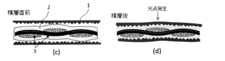
- (C) It is a schematic diagram which shows the state just before lamination
- (D) It is a schematic diagram which shows the state after lamination
- FRP precursor Fiber Reinforced Plastics
- a high elastic modulus material such as fiber is used as an aggregate, and the aggregate is placed in a matrix (matrix) such as plastic to improve the strength.
- Matrix matrix
- FRP can be used in a wide range of fields such as housing equipment, structural materials such as ships, vehicles and aircraft, and electronic equipment.
- FRP utilized for an electronic device the laminated board containing the prepreg for printed wiring boards, etc. are mentioned.
- a prepreg is mentioned as a FRP precursor for printed wiring boards.
- the FRP precursor of the present invention has a surface waviness of 12 ⁇ m or less on both sides thereof.
- the surface waviness can be obtained from a waviness curve according to ISO 4287 (1997). JIS B 0601 (2001) may be used instead of ISO 4287 (1997).
- For the waviness curve reference can be made to 3.1.7 of JIS B 0601 (2001).
- the surface waviness in the present invention is a surface waviness (also referred to as a waviness parameter) measured using “Surf Test SV-3200” (manufactured by Mitutoyo Corporation) as a surface roughness measuring device.
- the surface waviness is “both sides” surface waviness of the FRP precursor. For example, even if the surface waviness on one side is 12 ⁇ m or less, the surface waviness on the other side exceeds 12 ⁇ m. FRP precursors that are present are not included in the present invention.
- the surface waviness of the FRP precursor of the present invention is preferably 10 ⁇ m or less, more preferably 9 ⁇ m or less.
- the lower limit is not particularly limited, but may be 2 ⁇ m, 4 ⁇ m, 5 ⁇ m, or 6 ⁇ m.
- the tent property of the metal foil is a property that maintains the flat state of the metal foil when the metal foil is supported by several fulcrums, and that the tent property of the metal foil is high. Means that the metal foil has a high property of maintaining a flat state without bending. Furthermore, if it is the FRP precursor of this invention, there is no need to divide the heat-pressing process at the time of manufacture of the laminated board mentioned later into two steps, and lamination conditions become industrially advantageous.
- FIG. 1 is a schematic diagram which shows the state just before lamination
- the FRP precursor (prepreg) processed so that the surface waviness is 12 ⁇ m or less is used, which corresponds to the present invention.
- (c) of FIG. 2 is a schematic diagram showing a state immediately before lamination in the conventional method for producing a metal-clad laminate.
- the FRP precursor (prepreg) prepared according to the conventional method is used as it is, the surface of the FRP precursor (prepreg) has a slight unevenness.
- a thin metal foil having a thickness of 12 ⁇ m is used.
- the results of producing a metal-clad laminate by heating and pressing these are shown in FIG. 1 (b) and FIG. 2 (d), respectively.
- FIG. 1B the surface undulation of the metal foil is small, and no light spot is generated.
- FIG. 2D it is considered that a light spot is likely to be generated as a result of the metal foil following the unevenness of the FRP precursor (prepreg).
- the FRP precursor of the present invention (hereinafter, the FRP precursor can be read as “prepreg”) is (1) a step of reducing the surface waviness on both sides of the FRP precursor to 12 ⁇ m or less [hereinafter, step (1) ). ] Can be manufactured by the manufacturing method of the FRP precursor which has.
- the FRP precursor used in step (1) before the surface waviness is reduced to 12 ⁇ m or less can be produced according to a conventional method. For example, if it is a prepreg, if it manufactured according to the manufacturing method of the normal prepreg mentioned later, it will correspond to the surface waviness exceeding 12 micrometers.
- the method for reducing the surface waviness to 12 ⁇ m or less is not particularly limited, and all methods that can be considered by those skilled in the art can be adopted.
- the FRP precursor is sandwiched from above and below, Examples thereof include a method of heating and pressurizing with a vacuum laminator and the like, and (ii) a method of laminating a thermosetting resin film on both surfaces of the FRP precursor.
- the surface undulation of the FRP precursor is reduced to 12 ⁇ m or less by sandwiching the FRP precursor between the release films and then heating and pressing it.
- release films include organic films such as polyethylene terephthalate (PET), biaxially oriented polypropylene (OPP), polyethylene, polyvinyl fluorate, and polyimide; films of copper, aluminum, and alloys of these metals, or these organic films or metals.
- PET polyethylene terephthalate
- OPP biaxially oriented polypropylene
- polyethylene polyethylene
- polyvinyl fluorate polyvinyl fluorate
- polyimide polyimide
- films of copper, aluminum, and alloys of these metals, or these organic films or metals are mentioned.
- the heating and pressing conditions are not particularly limited, and may be set within a range usually employed by those skilled in the art.
- the heating temperature is preferably 80 to 180 ° C, more preferably 100 to 150 ° C.
- the load pressure when the FRP precursor sandwiched between the release films is pressurized is preferably 0.1 to 5 MPa, more preferably 0.1 to 2 MPa.
- the heating time is preferably 5 to 60 seconds, more preferably 5 to 40 seconds before pressurization, and preferably 10 to 60 seconds, more preferably 15 to 45 seconds while pressurizing the FRP precursor. is there.
- the degree of vacuum is preferably ⁇ 80 kPa (G) or less, more preferably ⁇ 90 kPa (G) or less.
- thermosetting resin film although it does not restrict
- the film formed using the thermosetting resin composition mentioned later can be used. More specifically, a film formed by drying a thermosetting resin composition described later to remove the organic solvent and semi-curing the thermosetting resin composition can be used.
- the thickness of the thermosetting resin film (the thickness of the thermosetting resin portion) is preferably 3 to 50 ⁇ m, more preferably 3 to 30 ⁇ m, still more preferably 3 to 15 ⁇ m, and particularly preferably 3 to 10 ⁇ m.
- thermosetting resin composition is applied to a release film, an unnecessary organic solvent is removed and then thermoset to form a film, and then heat laminated to a glass cloth.
- a method of simultaneously preparing the FRP precursor and reducing the surface waviness can also be employed.
- the prepreg which is one of the FRP precursors will be specifically described.
- the prepreg contains a reinforcing base material and a thermosetting resin composition.
- the reinforcing base material for the prepreg well-known materials used for various types of laminates for electrical insulating materials can be used.
- the material of the reinforcing substrate includes natural fibers such as paper and cotton linter; inorganic fibers such as glass fibers and asbestos; organic fibers such as aramid, polyimide, polyvinyl alcohol, polyester, tetrafluoroethylene, and acrylic; a mixture thereof Is mentioned.
- glass fiber is preferable from the viewpoint of flame retardancy.
- Glass fiber base materials include woven fabrics using E glass, C glass, D glass, S glass, etc., or glass woven fabrics obtained by bonding short fibers with an organic binder; glass fibers mixed with cellulose fibers, etc. Can be mentioned. More preferably, it is a glass woven fabric using E glass.
- These reinforcing substrates have a shape such as a woven fabric, a nonwoven fabric, a low-ink, a chopped strand mat, or a surfacing mat.
- a material and a shape are selected by the use and performance of the target molding, and 1 type may be used independently and 2 or more types of materials and shapes can also be combined as needed.
- the prepreg can be produced by, for example, impregnating or coating a reinforcing base material with a thermosetting resin composition, and semi-curing (B-stage) by removing the organic solvent and thermosetting.
- the heating temperature at the time of semi-curing (B-stage) is the temperature above the boiling point of the organic solvent, that is, the organic solvent removal efficiency is good because it also removes the organic solvent, that is, preferably 80 to 200 ° C.
- the temperature is preferably 140 to 180 ° C.
- the prepreg obtained by semi-curing (B stage) is regarded as an uncured prepreg, and the C prepreg is regarded as a cured prepreg.
- thermosetting resin composition contains at least a thermosetting resin.
- a curing agent if necessary, a curing accelerator, an inorganic filler, an organic filler, a coupling agent, a leveling agent, an antioxidant, a flame retardant, a flame retardant aid, a thixotropic agent.
- examples include an imparting agent, a thickener, a thixotropic agent, a flexible material, a surfactant, a photopolymerization initiator, and the like, and preferably contains at least one selected from these.
- each component which a thermosetting resin composition contains is demonstrated in order.
- thermosetting resin epoxy resins, phenol resins, unsaturated imide resins, cyanate resins, isocyanate resins, benzoxazine resins, oxetane resins, amino resins, unsaturated polyester resins, allyl resins, dicyclopentadiene resins, silicone resins, A triazine resin, a melamine resin, etc. are mentioned. Moreover, it does not restrict
- Epoxy resins include cresol novolac type epoxy resin, phenol novolac type epoxy resin, naphthol novolak type epoxy resin, aralkyl novolac type epoxy resin, biphenyl novolac type epoxy resin, bisphenol A type epoxy resin, bisphenol F type epoxy resin, bisphenol S type.
- Epoxy resin bisphenol T type epoxy resin, bisphenol Z type epoxy resin, tetrabromobisphenol A type epoxy resin, biphenyl type epoxy resin, tetramethylbiphenyl type epoxy resin, triphenyl type epoxy resin, tetraphenyl type epoxy resin, naphthol aralkyl type Epoxy resin, naphthalene all aralkyl epoxy resin, naphthol aralkyl epoxy resin, fluorene epoxy resin , An epoxy resin having a dicyclopentadiene skeleton, epoxy resins having an ethylenically unsaturated group in the backbone, the alicyclic type epoxy resins.
- An epoxy resin may be used individually by 1 type, and may use 2 or more types together from a viewpoint of insulation reliability and heat resistance.
- Commercially available epoxy resins include “EPICLON (registered trademark) N-660” (made by DIC Corporation), which is a cresol novolac type epoxy resin, and “EPICLON (registered trademark) 840S” (DIC), which is a bisphenol A type epoxy resin. Co., Ltd.), “jER828EL”, “YL980” (manufactured by Mitsubishi Chemical Corporation), and the like.
- the epoxy resin is not particularly limited. From the viewpoint of imparting flexibility, the epoxy resin has two or more epoxy groups in one molecule, and an alkylene glycol having 3 or more carbon atoms in the alkylene group. It may be an epoxy resin having a derived structural unit in the main chain. Further, from the viewpoint of further improving flexibility, two or more structural units derived from an alkylene glycol having 3 or more carbon atoms in the alkylene group may be continuously repeated.
- the alkylene glycol having 3 or more carbon atoms in the alkylene group is preferably an alkylene glycol having 4 or more carbon atoms in the alkylene group.
- the upper limit of the carbon number of the alkylene group is not particularly limited, but is preferably 15 or less, more preferably 10 or less, and still more preferably 8 or less.
- an epoxy resin you may use a halogenated epoxy resin from a flame-retardant viewpoint.
- thermosetting resin is an epoxy resin
- epoxy resins such as phenolic curing agents, cyanate ester curing agents, acid anhydride curing agents, amine curing agents, active ester group-containing compounds, etc. Examples thereof include a curing agent.
- a thermosetting resin is resin other than an epoxy resin
- a well-known thing can be used as the hardening
- curing agent may be used individually by 1 type, and may use 2 or more types together.
- curing agent a biphenyl type hardening
- phenolic curing agents examples include cresol novolac type curing agents such as KA-1160, KA-1163, and KA-1165 (all manufactured by DIC Corporation); MEH-7700, MEH-7810, MEH-7851 (any Biphenyl type curing agent such as Phenolite (registered trademark) TD2090 (made by DIC Corporation); naphthylene ether type such as EXB-6000 (made by DIC Corporation)
- Hardeners Triazine skeleton-containing phenolic hardeners such as LA3018, LA7052, LA7054, and LA1356 (all manufactured by DIC Corporation).
- the cyanate ester curing agent is not particularly limited, but is bisphenol A dicyanate, polyphenol cyanate (oligo (3-methylene-1,5-phenylene cyanate), 4,4′-methylenebis (2,6-dimethylphenyl cyanate).
- the acid anhydride curing agent is not particularly limited, but phthalic anhydride, tetrahydrophthalic anhydride, hexahydrophthalic anhydride, methyltetrahydrophthalic anhydride, methylhexahydrophthalic anhydride, methylnadic anhydride, hydrogen Methyl nadic anhydride, trialkyltetrahydrophthalic anhydride, dodecenyl succinic anhydride, 5- (2,5-dioxotetrahydro-3-furanyl) -3-methyl-3-cyclohexene-1,2-dicarboxylic anhydride Products, trimellitic anhydride, pyromellitic anhydride, and the like.
- the amine curing agent is not particularly limited, but includes aliphatic amines such as triethylenetetramine, tetraethylenepentamine, and diethylaminopropylamine; aromatic amines such as metaphenylenediamine and 4,4′-diaminodiphenylmethane, and the like. Can be mentioned. Moreover, urea resin etc. can also be used as a hardening
- thermosetting resin composition contains a curing agent
- the content thereof is preferably 20 to 150 parts by mass, more preferably 20 to 100 parts by mass, and still more preferably 100 parts by mass of the thermosetting resin. 40 to 100 parts by mass.
- the content may be represented using a functional group equivalent, and it is preferable to do so.
- the curing agent may be added so that (mass of thermosetting resin / functional group equivalent) ⁇ (mass of curing agent / functional group equivalent capable of reacting with thermosetting resin) ⁇ constant C. preferable.
- the constant C varies depending on the type of functional group of the curing agent, and is preferably 0.8 to 1.2 when the functional group is a phenolic hydroxyl group, and 0.2 to 0.4 when the functional group is an amino group. In the case of an active ester group, 0.3 to 0.6 is preferable.
- the thermosetting resin is an epoxy resin
- the above formula becomes (mass of epoxy resin / epoxy group equivalent) ⁇ (mass of curing agent / functional group equivalent capable of reacting with epoxy group) ⁇ constant C.
- thermosetting resin As a hardening accelerator, the general hardening accelerator used for hardening of the said thermosetting resin can be used.
- the thermosetting resin is an epoxy resin
- examples of the curing accelerator include imidazole compounds and derivatives thereof; phosphorus compounds; tertiary amine compounds; quaternary ammonium compounds. From the viewpoint of promoting the curing reaction, imidazole compounds and derivatives thereof are preferred.
- imidazole compound and derivatives thereof include 2-methylimidazole, 2-ethylimidazole, 2-undecylimidazole, 2-heptadecylimidazole, 2-phenylimidazole, 1,2-dimethylimidazole, 2-ethyl-1 -Methylimidazole, 1,2-diethylimidazole, 1-ethyl-2-methylimidazole, 2-ethyl-4-methylimidazole, 4-ethyl-2-methylimidazole, 1-isobutyl-2-methylimidazole, 2-phenyl -4-methylimidazole, 1-benzyl-2-phenylimidazole, 1-cyanoethyl-2-methylimidazole, 1-cyanoethyl-2-ethylimidazole, 1-cyanoethyl-2-phenylimidazole, 1-cyanoethyl-2-ethyl- 4-me Ruimidazole, 2-methylimid
- An imidazole compound may be used individually by 1 type, and may use 2 or more types together.
- thermosetting resin composition contains a curing accelerator
- the content thereof is preferably 0.1 to 20 parts by mass, more preferably 0.1 to 10 parts by mass with respect to 100 parts by mass of the thermosetting resin. Part, more preferably 0.5 to 6 parts by weight.
- Inorganic filler The inorganic filler can reduce the coefficient of thermal expansion and improve the coating strength.
- Inorganic fillers include silica, alumina, barium sulfate, talc, mica, kaolin, boehmite, beryllia, barium titanate, potassium titanate, strontium titanate, calcium titanate, aluminum carbonate, magnesium hydroxide, aluminum hydroxide, Aluminum borate, aluminum silicate, calcium carbonate, calcium silicate, magnesium silicate, zinc borate, zinc stannate, aluminum oxide, zirconia, mullite, magnesia, zinc oxide, titanium oxide, silicon carbide, silicon nitride, boron nitride And clays such as calcined clay, short glass fibers, glass powder, hollow glass beads, and the like, and at least one selected from the group consisting of these is preferably used.
- the glass include E glass, T glass, and D glass.
- silica and alumina are preferable and silica is more preferable from the viewpoints of reduction of thermal expansion coefficient, relative dielectric constant, and dielectric loss tangent.
- the silica include precipitated silica produced by a wet method and having a high water content, and dry method silica produced by a dry method and containing almost no bound water or the like.
- the dry process silica include crushed silica, fumed silica, and fused silica (fused spherical silica) depending on the production method.
- the inorganic filler may be surface-treated with a surface treatment agent such as a silane coupling agent in order to improve moisture resistance, or may be hydrophobized to improve dispersibility.
- the inorganic filler can be appropriately selected depending on the purpose. From the viewpoint of facilitating the formation of fine wiring, the specific surface area of the inorganic filler is preferably 20 m 2 / g or more, more preferably 30 to 250 m 2 / g, still more preferably 100 to 250 m 2 / g.
- the specific surface area of the inorganic filler can be determined by a measurement method usually performed by those skilled in the art, and can be measured, for example, by the BET method.
- the BET method is a method in which molecules having a known adsorption occupation area are adsorbed on the surface of powder particles at the temperature of liquid nitrogen, and the specific surface area of the sample is obtained from the amount. In the specific surface area analysis, the BET method using an inert gas such as nitrogen is most often used.
- the inorganic filler preferably contains an inorganic filler having an average primary particle size of 100 nm or less, more preferably 1 to 80 nm, still more preferably 1 to 50 nm, and still more preferably 5 to 30 nm. It is preferable to contain an inorganic filler, particularly preferably an inorganic filler of 10 to 30 nm.
- the “average primary particle diameter” refers to the average diameter of aggregated particles, that is, the average particle diameter of a single substance that is not aggregated, not the secondary particle diameter. The primary average particle diameter can be determined by measuring with a laser diffraction particle size distribution meter.
- the average primary particle size is the particle size at a point corresponding to a volume of 50% when a cumulative frequency distribution curve based on the particle size is obtained with the total particle volume as 100%.
- an inorganic filler having an average primary particle diameter of 0.1 to 50 ⁇ m may be further contained.
- the average primary particle diameter of the inorganic filler is more preferably 0.1 to 30 ⁇ m, further preferably 0.5 to 15 ⁇ m, and particularly preferably 0.5 to 7 ⁇ m.
- the content of the inorganic filler is more preferably 5 to 50% by volume, still more preferably 10 to 40% by volume.
- a coupling agent By including the coupling agent, there are the effects of improving the dispersibility of the inorganic filler and the organic filler and improving the adhesion to the reinforcing substrate and the metal foil.
- a coupling agent may be used individually by 1 type, and may use 2 or more types together.
- As the coupling agent a silane coupling agent is preferable.
- silane coupling agents include aminosilane coupling agents [eg, 3-aminopropyltrimethoxysilane, N- (2-aminoethyl) -3-aminopropyltriethoxysilane, etc.], epoxysilane coupling agents [ For example, 3-glycidoxypropyltrimethoxysilane, 2- (3,4-epoxycyclohexyl) ethyltrimethoxysilane, etc.], phenylsilane coupling agents, alkylsilane coupling agents, alkenylsilane coupling agents [ For example, vinyl silane coupling agents such as vinyl trichlorosilane and vinyl triethoxy silane], alkynyl silane coupling agents, haloalkyl silane coupling agents, siloxane coupling agents, hydrosilane coupling agents, silazane cups Coupling agent, alkoxysilane coupling agent, chlorosilane coupling agent, (me
- thermosetting resin composition contains a coupling agent
- the content thereof is preferably 0.1 to 20 parts by mass, more preferably 0.1 to 10 parts by mass with respect to 100 parts by mass of the thermosetting resin. Part, more preferably 0.5 to 6 parts by weight.
- the resin composition may further contain an organic solvent.
- the resin composition containing an organic solvent may be referred to as a resin varnish.
- the organic solvent is not particularly limited, but methanol, ethanol, propanol, butanol, methyl cellosolve, butyl cellosolve, propylene glycol monomethyl ether, ethylene glycol monoethyl ether, dipropylene glycol monomethyl ether, dipropylene glycol monoethyl ether, tripropylene Alcohol solvents such as glycol monomethyl ether; ketone solvents such as acetone, methyl ethyl ketone, methyl isobutyl ketone, butanone, cyclohexanone and 4-methyl-2-pentanone; ester solvents such as ethyl acetate, butyl acetate and propylene glycol monomethyl ether acetate Ether solvents such as tetrahydrofuran; aromatic
- a ketone solvent is preferable, cyclohexanone, methyl ethyl ketone, and methyl isobutyl ketone are more preferable, and cyclohexanone and methyl ethyl ketone are more preferable.
- An organic solvent may be used individually by 1 type, and may use 2 or more types together.
- the content of the organic solvent is adjusted, for example, so that the nonvolatile content of the resin composition is preferably 20 to 85% by mass, more preferably 40 to 80% by mass. To do.
- thermosetting resin composition may be directly stirred and mixed at a temperature at which curing of the thermosetting resin composition does not proceed remarkably and at a temperature at which the thermosetting resin composition liquefies.
- thermosetting resin composition There is no restriction
- a thermosetting resin and other components as necessary may be added to the solvent, and then mixed and stirred using various mixers to prepare a resin varnish.
- the mixer include an ultrasonic dispersion method, a high-pressure collision dispersion method, a high-speed rotation dispersion method, a bead mill method, a high-speed shear dispersion method, and a rotation and revolution dispersion method.
- the present invention also provides a metal-clad laminate having a metal foil on the laminate along with the laminate containing the FRP precursor (prepreg).
- the laminate of the present invention is (1) a step of reducing the surface waviness on both sides of the FRP precursor to 12 ⁇ m or less, and (2) a step of laminating two or more FRP precursors obtained in the step (1), It can manufacture with the manufacturing method of the laminated board which has.
- the metal-clad laminate of the present invention is (1) a step of reducing the surface waviness on both sides of the FRP precursor to 12 ⁇ m or less; (2) a step of laminating two or more FRP precursors obtained in the step (1), and (3) a step of providing a metal foil on the laminate obtained in the step (2), It can manufacture by the manufacturing method of the metal-clad laminated board which has.
- a laminated board can be produced by laminating and forming two or more, preferably 2 to 20, sheets of the FRP precursor (prepreg).
- a substrate on which inner layer circuit processing has been performed may be sandwiched between FRP precursors (prepregs).
- a metal-clad laminate is obtained by laminating two or more of the FRP precursors (prepregs), preferably 2 to 20, and laminating the metal foil on one or both sides, preferably both sides.
- a lamination condition in the step (2) a known condition used for production of a laminate can be employed. For example, a multi-stage press, a multi-stage vacuum press, continuous molding, an autoclave molding machine, etc.
- the thickness of the metal foil is preferably 40 ⁇ m or less, more preferably 1 to 40 ⁇ m, still more preferably 5 to 40 ⁇ m, particularly preferably 5 to 35 ⁇ m, and most preferably 5 to 5 ⁇ m from the viewpoint of remarkably expressing the effects of the present invention. It is 25 ⁇ m, particularly preferably 5 to 17 ⁇ m.
- metal of the metal foil from the viewpoint of conductivity, copper, gold, silver, nickel, platinum, molybdenum, ruthenium, aluminum, tungsten, iron, titanium, chromium, or at least one of these metal elements is included.
- An alloy is preferred.
- the alloy a copper alloy, an aluminum alloy, and an iron alloy are preferable.
- the copper-based alloy include a copper-nickel alloy.
- the iron-based alloy include an iron-nickel alloy (42 alloy).
- copper, nickel, and 42 alloy are more preferable, and copper is more preferable from a viewpoint of availability and cost.
- a printed wiring board can be manufactured by forming a wiring pattern in the said laminated board.
- the method of forming the wiring pattern is not particularly limited, but a subtractive method, a full additive method, a semi-additive method (SAP) or a modified semi-additive process (m-SAP), etc. There are known methods.
- the semiconductor package of the present invention contains the printed wiring board of the present invention. More specifically, the semiconductor package is formed by mounting a semiconductor on the printed wiring board of the present invention.
- the semiconductor package of the present invention can be manufactured by mounting a semiconductor chip, a memory or the like at a predetermined position of the printed wiring board of the present invention.
- the surface undulation obtained from the undulation curve was measured according to ISO 4287 (1997) using the prepreg before lamination produced in each example or the copper clad laminate. More specifically, surface waviness (waviness parameter) was measured using a surface roughness measuring instrument “Surf Test SV-3200” (manufactured by Mitutoyo Corporation) as a measuring device. In addition, the surface waviness was measured on both sides, and the larger value was adopted.
- thermosetting resin varnish 1 Cresol novolak type epoxy resin “EPICLON (registered trademark) N-660” (manufactured by DIC Corporation) 100 parts by mass, bisphenol A type epoxy To 30 parts by mass of cyclohexanone and 120 parts by mass of methyl ethyl ketone was added to 10 parts by mass of the resin “EPICLON 840S” (manufactured by DIC Corporation) and 60 parts by mass of the phenol novolac resin “Phenolite (registered trademark) TD2090” (manufactured by DIC Corporation). Stir well and dissolve.
- Cresol novolak type epoxy resin “EPICLON (registered trademark) N-660” manufactured by DIC Corporation
- bisphenol A type epoxy To 30 parts by mass of cyclohexanone and 120 parts by mass of methyl ethyl ketone was added to 10 parts by mass of the resin “EPICLON 840S” (manufactured by DIC Corporation) and 60 parts by mass
- Example 1 Production of prepreg and copper-clad laminate (production of prepreg)
- the resin content after drying the thermosetting resin varnish 1 obtained in Preparation Example 1 on a glass cloth (basis weight 48 g / m 2 , IPC # 1080, substrate width 530 mm, manufactured by Nitto Boseki Co., Ltd.) is 62% by mass. It applied so that it might become. Subsequently, in order to semi-cure the thermosetting resin varnish 1 together with the removal of the organic solvent, it was heated in a hot air dryer at 160 ° C. to obtain a prepreg a.
- the prepreg a was sandwiched between upper and lower parts with a release aluminum foil “Seponium 202BC” (manufactured by Toyo Aluminum Chiba Co., Ltd.), and this was vacuumed at 120 ° C. with a vacuum laminator “MVLP500” (manufactured by Meiki Seisakusho Co., Ltd.). After being left for 20 seconds, the surface waviness was reduced by pressurizing from one side (load pressure: 0.5 MPa) and holding for 30 seconds at the same temperature, and prepreg A was produced. According to the above method, the surface undulation of the prepreg A was determined. The results are shown in Table 1.
- Example 2 In Example 1, instead of using a copper foil “GTS-12” (Furukawa Electric Co., Ltd.) having a thickness of 12 ⁇ m, a copper foil “GTS-35MP” (Furukawa Electric Co., Ltd.) having a thickness of 35 ⁇ m was used. Were similarly operated to produce a copper clad laminate. According to the said method, the surface waviness and the number of light spots of the obtained copper clad laminated board were measured. The results are shown in Table 1.
- Example 1 a copper-clad laminate was prepared by performing the same operation except that prepreg a was used instead of prepreg A when the copper-clad laminate was produced. The surface undulation and the number of light spots were measured. The results are shown in Table 1.
- Comparative Example 2 In Comparative Example 1, a 35 ⁇ m thick copper foil “GTS-35MP” (Furukawa Electric Co., Ltd.) was used instead of the 12 ⁇ m thick copper foil “GTS-12” (Furukawa Electric Co., Ltd.). Were similarly operated to produce a copper clad laminate. According to the said method, the surface waviness and the number of light spots of the obtained copper clad laminated board were measured. The results are shown in Table 1.
- thermosetting resin varnish 1 obtained in Preparation Example 1 was applied to a 580 mm wide PET film “G-2” (manufactured by Teijin DuPont Films Ltd.). At this time, the coating amount was adjusted so that the coating width was 525 mm and the thickness was 5 ⁇ m after drying. After application, the organic solvent was removed by drying, and the thermosetting resin varnish 1 was semi-cured to prepare a thermosetting resin film A ′.
- the thermosetting resin film A ′ was laminated on both surfaces of the prepreg a obtained in Example 1.
- the pressure roll conditions of the laminate were a normal temperature, a roll temperature of 110 ° C., a linear pressure of 0.25 MPa, and a speed of 2.0 m / min.
- Example 4 In Example 3, instead of using a 12 ⁇ m thick copper foil “GTS-12” (Furukawa Electric Co., Ltd.), a 35 ⁇ m thick copper foil “GTS-35MP” (Furukawa Electric Co., Ltd.) was used. Were similarly operated to produce a copper clad laminate. According to the said method, the surface waviness and the number of light spots of the obtained copper clad laminated board were measured. The results are shown in Table 1.
- the metal-clad laminate formed using the prepreg of the present invention is useful as a printed wiring board for electronic equipment because it has a small light spot and a small surface waviness even if the metal foil is 40 ⁇ m or less.
Landscapes
- Engineering & Computer Science (AREA)
- Chemical & Material Sciences (AREA)
- Microelectronics & Electronic Packaging (AREA)
- Manufacturing & Machinery (AREA)
- Materials Engineering (AREA)
- Textile Engineering (AREA)
- Inorganic Chemistry (AREA)
- Mechanical Engineering (AREA)
- Organic Chemistry (AREA)
- Chemical Kinetics & Catalysis (AREA)
- Medicinal Chemistry (AREA)
- Polymers & Plastics (AREA)
- Health & Medical Sciences (AREA)
- Crystallography & Structural Chemistry (AREA)
- Laminated Bodies (AREA)
- Reinforced Plastic Materials (AREA)
- Production Of Multi-Layered Print Wiring Board (AREA)
Abstract
Priority Applications (7)
| Application Number | Priority Date | Filing Date | Title |
|---|---|---|---|
| CN202410462921.3A CN118368804A (zh) | 2016-01-15 | 2017-01-13 | Frp前体、层叠板、覆金属层叠板、印刷布线板、半导体封装体及它们的制造方法 |
| JP2017561208A JP6981256B2 (ja) | 2016-01-15 | 2017-01-13 | Frp前駆体、積層板、金属張積層板、プリント配線板、半導体パッケージ、及びそれらの製造方法 |
| HK18114030.3A HK1254930A1 (zh) | 2016-01-15 | 2017-01-13 | Frp前体、层叠板、覆金属层叠板、印刷布线板、半导体封装体及它们的制造方法 |
| CN201780006411.3A CN108472831A (zh) | 2016-01-15 | 2017-01-13 | Frp前体、层叠板、覆金属层叠板、印刷布线板、半导体封装体及它们的制造方法 |
| US16/069,933 US20190037691A1 (en) | 2016-01-15 | 2017-01-13 | Frp precursor, laminated plate, metal-clad laminate, printed circuit board, semiconductor package, and method for producing same |
| EP17738572.1A EP3403801B1 (fr) | 2016-01-15 | 2017-01-13 | Précurseur de frp, plaque stratifiée, stratifié à revêtement métallique, carte de circuit imprimé, boîtier de semi-conducteur et procédé de production associé |
| KR1020187019670A KR102704853B1 (ko) | 2016-01-15 | 2017-01-13 | Frp 전구체, 적층판, 금속장 적층판, 프린트 배선판, 반도체 패키지 및 그들의 제조 방법 |
Applications Claiming Priority (2)
| Application Number | Priority Date | Filing Date | Title |
|---|---|---|---|
| JP2016006476 | 2016-01-15 | ||
| JP2016-006476 | 2016-01-15 |
Publications (1)
| Publication Number | Publication Date |
|---|---|
| WO2017122820A1 true WO2017122820A1 (fr) | 2017-07-20 |
Family
ID=59311190
Family Applications (1)
| Application Number | Title | Priority Date | Filing Date |
|---|---|---|---|
| PCT/JP2017/001134 Ceased WO2017122820A1 (fr) | 2016-01-15 | 2017-01-13 | Précurseur de frp, plaque stratifiée, stratifié à revêtement métallique, carte de circuit imprimé, boîtier de semi-conducteur et procédé de production associé |
Country Status (8)
| Country | Link |
|---|---|
| US (1) | US20190037691A1 (fr) |
| EP (1) | EP3403801B1 (fr) |
| JP (1) | JP6981256B2 (fr) |
| KR (1) | KR102704853B1 (fr) |
| CN (2) | CN118368804A (fr) |
| HK (1) | HK1254930A1 (fr) |
| TW (2) | TW202138441A (fr) |
| WO (1) | WO2017122820A1 (fr) |
Cited By (4)
| Publication number | Priority date | Publication date | Assignee | Title |
|---|---|---|---|---|
| US11264293B2 (en) * | 2017-07-24 | 2022-03-01 | Kyocera Corporation | Wiring board, electronic device package, and electronic device |
| WO2022255278A1 (fr) * | 2021-06-01 | 2022-12-08 | 昭和電工マテリアルズ株式会社 | Préimprégné, plaque stratifiée, plaque stratifiée plaquée de métal, carte de câblage imprimée, boîtier de semi-conducteur, procédé de fabrication de préimprégné et procédé de fabrication de plaque stratifiée plaquée de métal |
| WO2024122587A1 (fr) * | 2022-12-07 | 2024-06-13 | 株式会社レゾナック | Préimprégné, plaque stratifiée, plaque stratifiée à revêtement métallique, carte de câblage imprimée, boîtier de semi-conducteur, procédé de fabrication de préimprégné et procédé de fabrication de plaque stratifiée à revêtement métallique |
| WO2024122584A1 (fr) * | 2022-12-07 | 2024-06-13 | 株式会社レゾナック | Stratifié plaqué de métal, carte de circuit imprimé, boîtier de semi-conducteur et leur procédé de fabrication |
Families Citing this family (2)
| Publication number | Priority date | Publication date | Assignee | Title |
|---|---|---|---|---|
| TWI686293B (zh) * | 2019-06-21 | 2020-03-01 | 台燿科技股份有限公司 | 金屬箔積層板及其製法 |
| CN116135916B (zh) * | 2021-11-18 | 2025-10-31 | 台光电子材料(昆山)股份有限公司 | 一种填料、其制备方法、包含该填料的树脂组合物及其制品 |
Citations (7)
| Publication number | Priority date | Publication date | Assignee | Title |
|---|---|---|---|---|
| JPH11156851A (ja) * | 1997-11-27 | 1999-06-15 | Hitachi Chem Co Ltd | プリプレグの製造方法 |
| JP2004238465A (ja) * | 2003-02-05 | 2004-08-26 | Sumitomo Bakelite Co Ltd | 複合基板の製造方法 |
| JP2004342871A (ja) | 2003-05-16 | 2004-12-02 | Nec Toppan Circuit Solutions Inc | 多層プリント配線板及びその製造方法 |
| JP2007039495A (ja) * | 2005-08-01 | 2007-02-15 | Sumitomo Bakelite Co Ltd | 基板の製造方法 |
| JP2010147443A (ja) * | 2008-12-22 | 2010-07-01 | Panasonic Electric Works Co Ltd | 積層板の製造方法 |
| WO2011024870A1 (fr) * | 2009-08-26 | 2011-03-03 | 旭化成イーマテリアルズ株式会社 | Tissu de verre pour carte de câblages imprimés |
| JP2013129827A (ja) * | 2011-11-25 | 2013-07-04 | Sumitomo Bakelite Co Ltd | プリプレグ、積層板、多層プリント配線板、および半導体装置 |
Family Cites Families (4)
| Publication number | Priority date | Publication date | Assignee | Title |
|---|---|---|---|---|
| CN1206546A (zh) * | 1996-10-25 | 1999-01-27 | 吉维迪意大利股份公司 | 用于印刷电路的采用单向性玻璃织物的叠层 |
| JP2000327814A (ja) * | 1999-05-19 | 2000-11-28 | Mitsubishi Rayon Co Ltd | プリプレグ及びこれを用いた管状成形体 |
| TWI252721B (en) * | 2004-09-10 | 2006-04-01 | Nan Ya Printed Circuit Board C | Method of manufacturing double-sided printed circuit board |
| KR101708941B1 (ko) * | 2009-10-14 | 2017-02-21 | 스미토모 베이클리트 컴퍼니 리미티드 | 에폭시 수지 조성물, 프리프레그, 금속 부착 적층판, 프린트 배선판 및 반도체 장치 |
-
2017
- 2017-01-13 HK HK18114030.3A patent/HK1254930A1/zh unknown
- 2017-01-13 CN CN202410462921.3A patent/CN118368804A/zh active Pending
- 2017-01-13 CN CN201780006411.3A patent/CN108472831A/zh active Pending
- 2017-01-13 WO PCT/JP2017/001134 patent/WO2017122820A1/fr not_active Ceased
- 2017-01-13 JP JP2017561208A patent/JP6981256B2/ja active Active
- 2017-01-13 EP EP17738572.1A patent/EP3403801B1/fr active Active
- 2017-01-13 KR KR1020187019670A patent/KR102704853B1/ko active Active
- 2017-01-13 US US16/069,933 patent/US20190037691A1/en not_active Abandoned
- 2017-01-16 TW TW110120127A patent/TW202138441A/zh unknown
- 2017-01-16 TW TW106101398A patent/TWI790989B/zh active
Patent Citations (7)
| Publication number | Priority date | Publication date | Assignee | Title |
|---|---|---|---|---|
| JPH11156851A (ja) * | 1997-11-27 | 1999-06-15 | Hitachi Chem Co Ltd | プリプレグの製造方法 |
| JP2004238465A (ja) * | 2003-02-05 | 2004-08-26 | Sumitomo Bakelite Co Ltd | 複合基板の製造方法 |
| JP2004342871A (ja) | 2003-05-16 | 2004-12-02 | Nec Toppan Circuit Solutions Inc | 多層プリント配線板及びその製造方法 |
| JP2007039495A (ja) * | 2005-08-01 | 2007-02-15 | Sumitomo Bakelite Co Ltd | 基板の製造方法 |
| JP2010147443A (ja) * | 2008-12-22 | 2010-07-01 | Panasonic Electric Works Co Ltd | 積層板の製造方法 |
| WO2011024870A1 (fr) * | 2009-08-26 | 2011-03-03 | 旭化成イーマテリアルズ株式会社 | Tissu de verre pour carte de câblages imprimés |
| JP2013129827A (ja) * | 2011-11-25 | 2013-07-04 | Sumitomo Bakelite Co Ltd | プリプレグ、積層板、多層プリント配線板、および半導体装置 |
Cited By (8)
| Publication number | Priority date | Publication date | Assignee | Title |
|---|---|---|---|---|
| US11264293B2 (en) * | 2017-07-24 | 2022-03-01 | Kyocera Corporation | Wiring board, electronic device package, and electronic device |
| WO2022255278A1 (fr) * | 2021-06-01 | 2022-12-08 | 昭和電工マテリアルズ株式会社 | Préimprégné, plaque stratifiée, plaque stratifiée plaquée de métal, carte de câblage imprimée, boîtier de semi-conducteur, procédé de fabrication de préimprégné et procédé de fabrication de plaque stratifiée plaquée de métal |
| WO2022254587A1 (fr) * | 2021-06-01 | 2022-12-08 | 昭和電工マテリアルズ株式会社 | Préimprégné, plaque stratifiée, plaque stratifiée revêtue de métal, carte de circuit imprimé, boîtier de semi-conducteur, procédé de fabrication de préimprégné et procédé de fabrication de plaque stratifiée revêtue de métal |
| JPWO2022255278A1 (fr) * | 2021-06-01 | 2022-12-08 | ||
| JP7586317B2 (ja) | 2021-06-01 | 2024-11-19 | 株式会社レゾナック | プリプレグ、積層板、金属張り積層板、プリント配線板、半導体パッケージ並びにプリプレグの製造方法及び金属張り積層板の製造方法 |
| WO2024122587A1 (fr) * | 2022-12-07 | 2024-06-13 | 株式会社レゾナック | Préimprégné, plaque stratifiée, plaque stratifiée à revêtement métallique, carte de câblage imprimée, boîtier de semi-conducteur, procédé de fabrication de préimprégné et procédé de fabrication de plaque stratifiée à revêtement métallique |
| WO2024122584A1 (fr) * | 2022-12-07 | 2024-06-13 | 株式会社レゾナック | Stratifié plaqué de métal, carte de circuit imprimé, boîtier de semi-conducteur et leur procédé de fabrication |
| JP7529188B1 (ja) * | 2022-12-07 | 2024-08-06 | 株式会社レゾナック | 金属張積層板、プリント配線板及び半導体パッケージ並びにこれらの製造方法 |
Also Published As
| Publication number | Publication date |
|---|---|
| KR102704853B1 (ko) | 2024-09-06 |
| EP3403801B1 (fr) | 2022-03-02 |
| EP3403801A1 (fr) | 2018-11-21 |
| TW201736459A (zh) | 2017-10-16 |
| TWI790989B (zh) | 2023-02-01 |
| HK1254930A1 (zh) | 2019-08-02 |
| CN118368804A (zh) | 2024-07-19 |
| KR20180103061A (ko) | 2018-09-18 |
| US20190037691A1 (en) | 2019-01-31 |
| JP6981256B2 (ja) | 2021-12-15 |
| CN108472831A (zh) | 2018-08-31 |
| EP3403801A4 (fr) | 2019-08-14 |
| TW202138441A (zh) | 2021-10-16 |
| JPWO2017122820A1 (ja) | 2018-11-01 |
Similar Documents
| Publication | Publication Date | Title |
|---|---|---|
| TWI738705B (zh) | 預浸體、印刷線路板、半導體封裝體、及印刷線路板的製造方法 | |
| JP7276400B2 (ja) | 金属張積層板、プリント配線板及び半導体パッケージ | |
| JP6981256B2 (ja) | Frp前駆体、積層板、金属張積層板、プリント配線板、半導体パッケージ、及びそれらの製造方法 | |
| CN103917596A (zh) | 树脂组合物、使用了其的预浸料和层压板 | |
| JP7081231B2 (ja) | プリプレグ、積層板、プリント配線板、半導体パッケージ及びプリプレグの製造方法 | |
| WO2014088099A9 (fr) | Procédé de fabrication d'un stratifié revêtu d'une feuille métallique | |
| TWI737851B (zh) | 印刷線路板及半導體封裝體 | |
| WO2022254587A1 (fr) | Préimprégné, plaque stratifiée, plaque stratifiée revêtue de métal, carte de circuit imprimé, boîtier de semi-conducteur, procédé de fabrication de préimprégné et procédé de fabrication de plaque stratifiée revêtue de métal | |
| WO2018181513A1 (fr) | Procédé de fabrication d'un précurseur de frp et procédé de fabrication de frp | |
| HK40107367A (zh) | Frp前体、层叠板、覆金属层叠板、印刷布线板、半导体封装体及它们的制造方法 | |
| HK40104803A (zh) | 预浸渍体、印刷布綫板、半导体封装体及印刷布綫板的制造方法 | |
| JP7434707B2 (ja) | Frp前駆体、frp、積層板、金属張積層板、プリント配線板及び半導体パッケージ並びにfrp前駆体の製造方法 | |
| WO2025105228A1 (fr) | Procédés de production de stratifié, carte stratifiée, carte de circuit imprimé et boîtier de semi-conducteur | |
| WO2023218969A1 (fr) | Procédé de fabrication de précurseur de prv et procédé de fabrication de prv | |
| HK1261475B (zh) | 覆金属层叠板、印刷布綫板及半导体封装体 |
Legal Events
| Date | Code | Title | Description |
|---|---|---|---|
| 121 | Ep: the epo has been informed by wipo that ep was designated in this application |
Ref document number: 17738572 Country of ref document: EP Kind code of ref document: A1 |
|
| ENP | Entry into the national phase |
Ref document number: 2017561208 Country of ref document: JP Kind code of ref document: A |
|
| ENP | Entry into the national phase |
Ref document number: 20187019670 Country of ref document: KR Kind code of ref document: A |
|
| NENP | Non-entry into the national phase |
Ref country code: DE |
|
| WWE | Wipo information: entry into national phase |
Ref document number: 2017738572 Country of ref document: EP |
|
| ENP | Entry into the national phase |
Ref document number: 2017738572 Country of ref document: EP Effective date: 20180816 |