WO2017126204A1 - 受光素子、受光素子の製造方法、撮像素子および電子機器 - Google Patents
受光素子、受光素子の製造方法、撮像素子および電子機器 Download PDFInfo
- Publication number
- WO2017126204A1 WO2017126204A1 PCT/JP2016/083857 JP2016083857W WO2017126204A1 WO 2017126204 A1 WO2017126204 A1 WO 2017126204A1 JP 2016083857 W JP2016083857 W JP 2016083857W WO 2017126204 A1 WO2017126204 A1 WO 2017126204A1
- Authority
- WO
- WIPO (PCT)
- Prior art keywords
- layer
- photoelectric conversion
- light receiving
- receiving element
- conversion layer
- Prior art date
- Legal status (The legal status is an assumption and is not a legal conclusion. Google has not performed a legal analysis and makes no representation as to the accuracy of the status listed.)
- Ceased
Links
Images







Classifications
-
- H—ELECTRICITY
- H04—ELECTRIC COMMUNICATION TECHNIQUE
- H04N—PICTORIAL COMMUNICATION, e.g. TELEVISION
- H04N23/00—Cameras or camera modules comprising electronic image sensors; Control thereof
- H04N23/20—Cameras or camera modules comprising electronic image sensors; Control thereof for generating image signals from infrared radiation only
-
- H—ELECTRICITY
- H04—ELECTRIC COMMUNICATION TECHNIQUE
- H04N—PICTORIAL COMMUNICATION, e.g. TELEVISION
- H04N25/00—Circuitry of solid-state image sensors [SSIS]; Control thereof
- H04N25/70—SSIS architectures; Circuits associated therewith
-
- H—ELECTRICITY
- H10—SEMICONDUCTOR DEVICES; ELECTRIC SOLID-STATE DEVICES NOT OTHERWISE PROVIDED FOR
- H10F—INORGANIC SEMICONDUCTOR DEVICES SENSITIVE TO INFRARED RADIATION, LIGHT, ELECTROMAGNETIC RADIATION OF SHORTER WAVELENGTH OR CORPUSCULAR RADIATION
- H10F30/00—Individual radiation-sensitive semiconductor devices in which radiation controls the flow of current through the devices, e.g. photodetectors
- H10F30/20—Individual radiation-sensitive semiconductor devices in which radiation controls the flow of current through the devices, e.g. photodetectors the devices having potential barriers, e.g. phototransistors
-
- H—ELECTRICITY
- H10—SEMICONDUCTOR DEVICES; ELECTRIC SOLID-STATE DEVICES NOT OTHERWISE PROVIDED FOR
- H10F—INORGANIC SEMICONDUCTOR DEVICES SENSITIVE TO INFRARED RADIATION, LIGHT, ELECTROMAGNETIC RADIATION OF SHORTER WAVELENGTH OR CORPUSCULAR RADIATION
- H10F39/00—Integrated devices, or assemblies of multiple devices, comprising at least one element covered by group H10F30/00, e.g. radiation detectors comprising photodiode arrays
- H10F39/10—Integrated devices
-
- H—ELECTRICITY
- H10—SEMICONDUCTOR DEVICES; ELECTRIC SOLID-STATE DEVICES NOT OTHERWISE PROVIDED FOR
- H10F—INORGANIC SEMICONDUCTOR DEVICES SENSITIVE TO INFRARED RADIATION, LIGHT, ELECTROMAGNETIC RADIATION OF SHORTER WAVELENGTH OR CORPUSCULAR RADIATION
- H10F39/00—Integrated devices, or assemblies of multiple devices, comprising at least one element covered by group H10F30/00, e.g. radiation detectors comprising photodiode arrays
- H10F39/10—Integrated devices
- H10F39/12—Image sensors
-
- H—ELECTRICITY
- H10—SEMICONDUCTOR DEVICES; ELECTRIC SOLID-STATE DEVICES NOT OTHERWISE PROVIDED FOR
- H10F—INORGANIC SEMICONDUCTOR DEVICES SENSITIVE TO INFRARED RADIATION, LIGHT, ELECTROMAGNETIC RADIATION OF SHORTER WAVELENGTH OR CORPUSCULAR RADIATION
- H10F39/00—Integrated devices, or assemblies of multiple devices, comprising at least one element covered by group H10F30/00, e.g. radiation detectors comprising photodiode arrays
- H10F39/10—Integrated devices
- H10F39/12—Image sensors
- H10F39/18—Complementary metal-oxide-semiconductor [CMOS] image sensors; Photodiode array image sensors
- H10F39/184—Infrared image sensors
-
- H—ELECTRICITY
- H10—SEMICONDUCTOR DEVICES; ELECTRIC SOLID-STATE DEVICES NOT OTHERWISE PROVIDED FOR
- H10F—INORGANIC SEMICONDUCTOR DEVICES SENSITIVE TO INFRARED RADIATION, LIGHT, ELECTROMAGNETIC RADIATION OF SHORTER WAVELENGTH OR CORPUSCULAR RADIATION
- H10F39/00—Integrated devices, or assemblies of multiple devices, comprising at least one element covered by group H10F30/00, e.g. radiation detectors comprising photodiode arrays
- H10F39/80—Constructional details of image sensors
- H10F39/805—Coatings
- H10F39/8057—Optical shielding
-
- H—ELECTRICITY
- H10—SEMICONDUCTOR DEVICES; ELECTRIC SOLID-STATE DEVICES NOT OTHERWISE PROVIDED FOR
- H10F—INORGANIC SEMICONDUCTOR DEVICES SENSITIVE TO INFRARED RADIATION, LIGHT, ELECTROMAGNETIC RADIATION OF SHORTER WAVELENGTH OR CORPUSCULAR RADIATION
- H10F71/00—Manufacture or treatment of devices covered by this subclass
- H10F71/128—Annealing
-
- H—ELECTRICITY
- H10—SEMICONDUCTOR DEVICES; ELECTRIC SOLID-STATE DEVICES NOT OTHERWISE PROVIDED FOR
- H10F—INORGANIC SEMICONDUCTOR DEVICES SENSITIVE TO INFRARED RADIATION, LIGHT, ELECTROMAGNETIC RADIATION OF SHORTER WAVELENGTH OR CORPUSCULAR RADIATION
- H10F77/00—Constructional details of devices covered by this subclass
-
- H—ELECTRICITY
- H10—SEMICONDUCTOR DEVICES; ELECTRIC SOLID-STATE DEVICES NOT OTHERWISE PROVIDED FOR
- H10F—INORGANIC SEMICONDUCTOR DEVICES SENSITIVE TO INFRARED RADIATION, LIGHT, ELECTROMAGNETIC RADIATION OF SHORTER WAVELENGTH OR CORPUSCULAR RADIATION
- H10F77/00—Constructional details of devices covered by this subclass
- H10F77/10—Semiconductor bodies
- H10F77/12—Active materials
-
- Y—GENERAL TAGGING OF NEW TECHNOLOGICAL DEVELOPMENTS; GENERAL TAGGING OF CROSS-SECTIONAL TECHNOLOGIES SPANNING OVER SEVERAL SECTIONS OF THE IPC; TECHNICAL SUBJECTS COVERED BY FORMER USPC CROSS-REFERENCE ART COLLECTIONS [XRACs] AND DIGESTS
- Y02—TECHNOLOGIES OR APPLICATIONS FOR MITIGATION OR ADAPTATION AGAINST CLIMATE CHANGE
- Y02E—REDUCTION OF GREENHOUSE GAS [GHG] EMISSIONS, RELATED TO ENERGY GENERATION, TRANSMISSION OR DISTRIBUTION
- Y02E10/00—Energy generation through renewable energy sources
- Y02E10/50—Photovoltaic [PV] energy
Definitions
- the present disclosure relates to, for example, a light receiving element capable of detecting infrared rays, a manufacturing method thereof, an imaging element, and an electronic device.
- a light receiving element using a compound semiconductor as described above has a pn junction or a pin junction, and generates electrons and holes in the photoelectric conversion layer by light irradiation.
- a signal can be obtained by reading a change in current or voltage accompanying the generation of electrons and holes, and light detection is possible by so-called semiconductor photodiode operation.
- InGaAs is formed by epitaxial growth on, for example, an InP substrate, but short-infrared light can be detected because the band gap energy is smaller than that of silicon (Si).
- a plurality of pixels including photodiodes are arranged in an array.
- adjacent pixels adjacent photodiodes
- etching separation As a method for electrically separating adjacent pixels from each other, for example, etching separation can be cited.
- Patent Document 1 after forming a p-type semiconductor layer on the photoelectric conversion layer, a region between pixels (near the boundary between pixels) in the p-type semiconductor layer is selectively etched away. Thereafter, the p-type semiconductor layer separated for each pixel is connected to the electrode. In this way, electrical separation between adjacent pixels is achieved. Further, a region near the boundary between the pixels on the surface of the photoelectric conversion layer is covered with an insulating film such as silicon nitride (SiN) or silicon oxide (SiO 2 ).
- SiN silicon nitride
- SiO 2 silicon oxide
- the surface of the photoelectric conversion layer and the insulating film are in contact with each other in the region between the pixels.
- dark current is generated due to the interface defect.
- the dark current is a noise component, not a current generated by light incidence.
- the noise is large, the S / N ratio is small, so that the dynamic range of the obtained image is also small.
- a technique for suppressing image quality deterioration due to generation of dark current due to interface defects is desired.
- a light-receiving element includes a first compound semiconductor, a photoelectric conversion layer that absorbs wavelengths in the infrared region, and generates a charge; and a second compound semiconductor, and photoelectric conversion
- a plurality of contact layers provided on the layer with a gap between each other, a portion corresponding to the gap in the surface of the photoelectric conversion layer, and a side surface of each contact layer, and includes a group IV semiconductor And a coating layer.
- a manufacturing method of a light receiving element includes a first compound semiconductor, forms a photoelectric conversion layer that generates a charge by absorbing a wavelength in an infrared region, and includes a second compound semiconductor.
- a plurality of contact layers formed on the photoelectric conversion layer and spaced from each other, covering a portion of the surface of the photoelectric conversion layer corresponding to the gap and a side surface of each contact layer, and a group IV semiconductor Is formed.
- a plurality of contact layers including the second compound semiconductor are formed with a gap on the photoelectric conversion layer including the first compound semiconductor.
- a covering layer including a group IV semiconductor is formed so as to cover a portion of the surface of the photoelectric conversion layer corresponding to the gap and the side surface of each contact layer. That is, the portion of the photoelectric conversion layer corresponding to the gap between the contact layers is in contact with the coating layer containing a group IV semiconductor.
- the defect density is high at the interface.
- the interface defect density is reduced as compared with the case where the photoelectric conversion layer is in contact with the insulating film. Therefore, the generation of dark current due to interface defects is suppressed.
- An imaging device includes a plurality of pixels, a first compound semiconductor, a photoelectric conversion layer that absorbs wavelengths in the infrared region and generates charges, and a second compound semiconductor A plurality of contact layers provided on the photoelectric conversion layer with a gap between each other and for each pixel, a portion corresponding to the gap on the surface of the photoelectric conversion layer, and a side surface of each contact layer. And a coating layer containing a group IV semiconductor.
- An electronic apparatus includes the image sensor according to the embodiment of the present disclosure.
- the plurality of contact layers are provided on the photoelectric conversion layer including the first compound semiconductor with a gap between them.
- a covering layer including a group IV semiconductor is formed so as to cover a portion of the surface of the photoelectric conversion layer corresponding to the gap and the side surface of each contact layer.
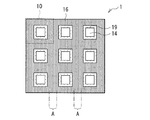
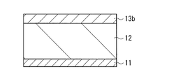
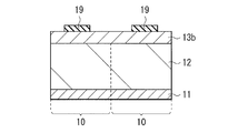
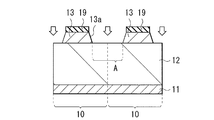
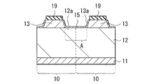
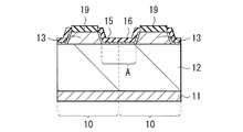
- FIG. 2 is a schematic diagram illustrating a planar configuration of the light receiving element illustrated in FIG. 1. It is sectional drawing for demonstrating 1 process of the manufacturing method of the light receiving element shown in FIG. It is sectional drawing showing the process of following FIG. 3A.
- FIG. 3B is a cross-sectional diagram illustrating a process following the process in FIG. 3B. It is sectional drawing for demonstrating 1 process of the manufacturing method of the light receiving element shown to FIG. 3B. It is sectional drawing showing the process of following FIG. 4A.
- FIG. 4B is a cross-sectional diagram illustrating a process following the process in FIG. 4B.
- FIG. 10 is a cross-sectional view illustrating a configuration of a light receiving element according to Modification 1.
- FIG. 10 is a cross-sectional view illustrating a configuration of a light receiving element according to Modification 2.
- FIG. 10 is a cross-sectional view illustrating a configuration of a light receiving element according to Modification 3.
- FIG. 10 is a cross-sectional view illustrating a configuration of a light receiving element according to Modification 3.
- FIG. 10 is a cross-sectional view illustrating a configuration of a light receiving element according to Modification 4.
- FIG. 11 is a cross-sectional view illustrating a configuration of a light receiving element according to Modification Example 5.
- FIG. 14 is a schematic diagram illustrating a planar configuration of the light receiving element illustrated in FIG. 13.
- 14 is a cross-sectional view illustrating a configuration of a light receiving element according to Modification 6.
- FIG. It is a block diagram showing the structure of an image sensor. It is a schematic diagram showing the structural example of a laminated type image pick-up element. It is a functional block diagram showing an example of the electronic device (camera) using the image pick-up element shown in FIG.
- Embodiment an example of a light receiving element having a covering layer containing a group IV semiconductor (Si) covering the surface of the photoelectric conversion layer and the side surface of the contact layer
- Modification 1 an example of a light receiving element having a coating layer containing another group IV semiconductor (Ge)
- Modification 3 an example of a light receiving element having a coating layer containing another group IV semiconductor (SiGe)) 4
- Modification 4 Example of light receiving element having a coating layer made of n-type Si 5).
- Modification 5 Example of a light receiving element having a coating layer containing an impurity element functioning as an n-type in the photoelectric conversion layer 6
- Modification 6 example of light receiving element provided with electrode for controlling potential of diffusion region of photoelectric conversion layer
- Modified example 7 example of a light receiving element having an insulating film containing a fixed charge on a coating layer 8
- Application example 1 example of image sensor
- Application Example 2 Example of electronic equipment
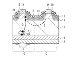
- FIG. 1 illustrates a cross-sectional configuration of a light receiving element (light receiving element 1) according to an embodiment of the present disclosure.
- FIG. 2 schematically shows a planar configuration of the light receiving element 1.
- the light receiving element 1 is applied to, for example, an infrared sensor using a compound semiconductor, and includes, for example, a plurality of light receiving unit regions 10 (corresponding to pixels P of an imaging element described later) arranged two-dimensionally. It is out.
- FIG. 1 shows a cross-sectional configuration of a portion corresponding to two pixels P.
- the light receiving element 1 has, for example, a photoelectric conversion layer 12 and a plurality of contact layers 13 in this order on a substrate 11.
- An electrode (first electrode 14) is electrically connected to each of the plurality of contact layers 13.
- a covering layer 15 and an insulating film 16 (first insulating film) are formed in this order so as to cover a part (surface 12a) of the surface of the photoelectric conversion layer 12 and a side surface (side surface 13a) of each contact layer 13. ing.
- a diffusion region 17 containing impurities is formed in a region adjacent to the coating layer 15 in the photoelectric conversion layer 12 and the contact layer 13.
- a second electrode 18 is formed on the surface of the substrate 11 opposite to the photoelectric conversion layer 12.
- the back surface of the second electrode 18 is a light incident surface S ⁇ b> 1 (configured so that infrared IR is incident from the second electrode 18 side).
- an on-chip lens (not shown) or the like may be further provided on the light incident surface S1 side of the second electrode 18.
- a color filter may be arranged on the insulating film 16 and the first electrode 14.
- a silicon semiconductor substrate on which a pixel circuit for reading signals from each pixel 10 and various wirings is formed is laminated.
- the first electrode 14 and the second electrode 18 are electrically connected to various circuits formed on the silicon semiconductor substrate through, for example, bumps and vias.
- the substrate 11 is made of a compound semiconductor containing n-type impurities, for example.
- the compound semiconductor used for the substrate 11 include III-V semiconductors such as InP.
- the photoelectric conversion layer 12 is formed on the substrate 11 in contact with the substrate 11, but another layer may be interposed between the substrate 11 and the photoelectric conversion layer 12.
- the material of the layer interposed between the substrate 11 and the photoelectric conversion layer 12 include semiconductor materials such as InAlAs, Ge, Si, GaAs, and InP. It is desirable to select a matching material.
- the photoelectric conversion layer 12 includes, for example, a compound semiconductor that absorbs wavelengths in the infrared region (hereinafter referred to as infrared rays) and generates charges (electrons and holes).
- the photoelectric conversion layer 12 is continuously provided on the substrate 11 as a common layer to the plurality of pixels 10 (or the plurality of contact layers 13).
- the photoelectric conversion layer 12 is composed of, for example, an n-type or p-type compound semiconductor (first compound semiconductor).
- compound semiconductors used for the photoelectric conversion layer 12 include III-V group semiconductors such as InGaAs.
- the composition of the compound semiconductor of the photoelectric conversion layer 12 lattice-matched with the substrate 11 made of InP is In 0.53 Ga 0.47 As.
- the doping density when the photoelectric conversion layer 12 is n-type is, for example, 1.0 ⁇ 10 18 cm ⁇ 3 or less
- the doping density when the photoelectric conversion layer 12 is p-type is, for example, 1.0 ⁇ 10 16 cm ⁇ 3 or less. Is desirable.
- the n-type impurity include silicon (Si)
- examples of the p-type impurity include zinc (Zn).
- the contact layer 13 is made of, for example, a p-type compound semiconductor (second compound semiconductor).
- the compound semiconductor used for the contact layer 13 include a III-V group semiconductor such as InP.
- a plurality of contact layers 13 are arranged on the photoelectric conversion layer 12 with a gap (gap A) therebetween (separated). Each contact layer 13 is formed in an island shape for each pixel 10.
- the plurality of contact layers 13 are formed by removing a selective portion corresponding to the gap A by, for example, etching (by etching separation) in the manufacturing process.
- the III-V group semiconductor used for the photoelectric conversion layer 12 and the contact layer 13 is not limited to the above materials (InGaAs, InP).
- the photoelectric conversion layer 12 and the contact layer 13 include indium (In), gallium (Ga), aluminum (Al), arsenic (As), phosphorus (P), antimony (Sb), nitrogen (N), and the like.
- a compound semiconductor containing at least one of the above can be used. Examples other than InGaAs and InP include InGaAsP, InGaP, InAsSb, GaAsSb, InAlAs, and the like.
- the photoelectric conversion layer 12 and the contact layer 13 are not limited to the III-V group semiconductor as described above, but may be a compound semiconductor such as a II-VI group semiconductor. In addition, an intrinsic semiconductor may be used for the photoelectric conversion layer 12.
- a pn junction or a pin junction is formed for each pixel 10 in the light receiving element 1 by stacking the substrate 11, the photoelectric conversion layer 12, and the contact layer 13.
- the first electrode 14 is an electrode to which a voltage for reading out electric charges (for example, holes) generated in the photoelectric conversion layer 12 is supplied, and is formed for each pixel 10.
- a mask layer 19 having an opening H is provided on the contact layer 13, and the first electrode 14 is electrically connected to the contact layer 13 through the opening H of the mask layer 19.
- the constituent material of the first electrode 14 include titanium (Ti), tungsten (W), titanium nitride (TiN), platinum (Pt), gold (Au), germanium (Ge), nickel (Ni), and aluminum ( Al) or any alloy containing at least one of them.
- the 1st electrode 14 may be comprised from transparent conductive films, such as ITO (indium tin oxide), for example.
- the first electrode 14 corresponds to a specific example of “electrode” of the present disclosure.
- the covering layer 15 is formed so as to cover the surface 12 a corresponding to the gap A in the surface of the photoelectric conversion layer 12 and the side surface 13 a of each contact layer 13.
- the covering layer 15 includes a group IV semiconductor (a group element element or compound).
- the coating layer 15 includes, for example, silicon (Si) (as a main component).
- the covering layer 15 desirably covers the entire area excluding the first electrode 14 and the mask layer 19 in plan view.
- the thickness of the coating layer 15 is, for example, not less than 0.25 nm and not more than 100 nm, and preferably not less than 1 nm and not more than 10 nm. When the thickness is 1 nm or more, it is easy to ensure good coverage.
- dark current may be generated when the coverage is poor, the occurrence of dark current due to such coverage can be suppressed when the thickness is 1 nm or more. Further, current leakage may occur between the adjacent contact layers 13 through the coating layer 15, but when the thickness of the coating layer 15 is 10 nm or less, occurrence of such current leakage can be suppressed. .
- the insulating film 16 functions as a protective film for the light receiving element 1 and is an insulating film containing any of silicon, nitrogen (N), aluminum (Al), hafnium (Hf), and the like.
- the insulating film 16 includes silicon oxide (SiO 2 ).
- the insulating film 16 may be made of, for example, silicon nitride (SiN), silicon oxynitride (SiON), aluminum oxynitride (AlON), SiAlN, aluminum oxide (Al 2 O 3 ), AlSiO, hafnium oxide (HfO). 2 ) or HfAlO or the like may be contained.
- the insulating film 16 may be a single layer film or a laminated film.
- the diffusion region 17 is formed in a part of the photoelectric conversion layer 12 and the contact layer 13 (a part adjacent to the coating layer 15).
- the diffusion region 17 is a region in which an element contained in the coating layer 15 is diffused in a part of the photoelectric conversion layer 12 or the contact layer 13.
- the coating layer 15 is a film containing Si
- Si is diffused in the diffusion region 17 (the diffusion region 17 contains silicon).
- the diffusion region 17 is used to convert the element (for example, Si) contained in the coating layer 15 into the photoelectric conversion layer 12 and the contact layer. 13 can be formed by diffusing each of them.
- the diffusion region 17 is a region having a higher doping density than the surroundings in the photoelectric conversion layer 12.
- the second electrode 18 is provided on the back surface (light incident surface S1) of the substrate 11 as an electrode common to each pixel P, for example.
- the second electrode 18 is not necessarily formed over the entire back surface of the substrate 11 as long as it is electrically connected to the substrate 11. Alternatively, the second electrode 18 may not be provided.
- the second electrode 18 is made of, for example, a conductive film having a transmittance of at least 50% for light having a wavelength of 1.6 ⁇ m.
- the mask layer 19 is a hard mask or a resist mask made of an insulating material.
- a hard mask for example, it is an insulating film containing any one of silicon, nitrogen (N), aluminum (Al), hafnium (Hf), and the like. Examples include silicon oxide (SiO 2 ), silicon nitride (SiN), silicon oxynitride (SiON), aluminum oxynitride (AlON), SiAlN, aluminum oxide (Al 2 O 3 ), AlSiO, hafnium oxide (HfO 2 ). Or HfAlO etc. are mentioned.
- the light receiving element 1 can be manufactured as follows, for example. 3A to 4C show the manufacturing process of the main part of the light receiving element 1 in the order of steps.
- a photoelectric conversion layer 12 made of, for example, n-type (or p-type) InGaAs and a contact layer made of, for example, p-type InP, are formed on one surface of a substrate 11 made of, for example, n-type InP. 13b are epitaxially grown in order.
- a gas containing an n-type (or p-type) impurity is introduced to form the photoelectric conversion layer 12 as an n-type (or p-type) layer.
- the contact layer 13b is formed as a p-type layer by introducing a gas containing a p-type impurity, for example.
- a mask layer 19 made of any one of the above-described materials (for example, SiN) is formed for each pixel 10 on the contact layer 13b.
- a gap A is formed by removing a selective region (region near the boundary between the pixels 10) of the contact layer 13b by dry etching or wet etching, for example. Layer 13b is etched away). That is, a plurality of contact layers 13 are formed with a gap A therebetween.
- a coating layer 15 is formed.
- a film containing the IV group semiconductor for example, Si
- a technique such as sputtering deposition, electron beam deposition, resistance heating deposition, CVD (Chemical Vapor Deposition), or ALD (Atomic Layer Deposition).
- patterning is performed.
- the coating layer 15 is formed so as to cover the surface 12 a exposed from the contact layer 13 and the side surface 13 a of the contact layer 13 in the surface of the photoelectric conversion layer 12.
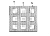
- FIG. 5 schematically shows a planar configuration after the coating layer 15 is formed.
- the covering layer 15 is formed so as to cover the entire region of the plurality of pixels 10 excluding the mask layer 19.
- the insulating film 16 is formed on the coating layer 15. Specifically, for example, thermal oxidation, using a technique such as CVD or ALD, after forming an insulating film 16 made of the above-described insulating material (e.g. SiO 2), is patterned.
- a technique such as CVD or ALD
- a diffusion region 17 is formed. Specifically, annealing treatment is performed.
- the annealing temperature at this time is preferably set to a temperature at which the group IV semiconductor atoms contained in the coating layer 15 are activated as a dopant.
- the group IV semiconductor atoms contained in the coating layer 15 for example, it can be set to 400 degrees or more and 800 degrees or less.
- the IV group semiconductor atom (for example, Si atom) contained in the coating layer 15 can be diffused in the adjacent photoelectric conversion layer 12 and the contact layer 13.
- the diffusion region 17 containing, for example, Si as an impurity is formed.
- This diffusion region 17 is a region (here, n-type region) having a higher doping density than the periphery thereof in the photoelectric conversion layer 12, and a region corresponding to the gap A in the photoelectric conversion layer 12 (near the boundary between the pixels 10). A potential barrier is formed in the region).
- annealing treatment is performed to diffuse the group IV semiconductor atoms from the coating layer 15 to form the diffusion region 17.
- the timing of forming the diffusion region 17 is limited to this. It may be after the coating layer 15 is formed.
- group IV semiconductor atoms can be diffused at the film forming temperature.
- the diffusion region 17 can be formed simultaneously with the formation of the insulating film 16.
- the first electrode 14 and the second electrode 18 made of the above-described material are formed.
- an opening H is formed in the mask layer 19 and then the opening H is formed through the opening H.
- the first electrode 14 is formed so as to be in contact with the contact layer 13.
- the light receiving element 1 shown in FIG. 1 is completed.
- the second electrode 18 If the second electrode 18 is not provided, voltage may be applied to the first electrode 14 so that a potential gradient is formed between the first electrode 14 and the substrate 11. However, by providing the second electrode 18, it is easy to form a larger potential gradient, and the other charge (electrons here) among the charges generated by the photoelectric conversion is passed through the second electrode 18 to the photoelectric conversion layer. 12 can be discharged.
- a plurality of contact layers 13 are arranged on the photoelectric conversion layer 12 with a gap A therebetween.
- a gap A between the plurality of contact layers 13 is formed by etching.
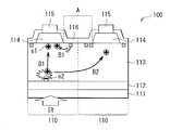
- FIG. 6 shows a cross-sectional configuration of a light receiving element (light receiving element 100) according to a comparative example of the present embodiment.
- a light receiving element 100 for example, an n-type photoelectric conversion layer 113 and a p-type contact layer 114 made of a compound semiconductor are formed in this order on a substrate 112.
- a plurality of contact layers 114 are formed by etching (with a gap A therebetween).
- a first electrode 115 is formed on the contact layer 114, and a second electrode 111 is formed on the light incident side surface of the substrate 112.
- an insulating film 116 made of SiN is formed so as to cover a portion of the surface of the photoelectric conversion layer 113 corresponding to the gap A and the side surface of the contact layer 114.
- the holes e1 and the electrons e2 are generated in the photoelectric conversion layer 113 by the incidence of infrared IR, the holes e1 move to the first electrode 115 side (D1), and the electrons e2 are on the second electrode 111 side. (D2).
- the photoelectric conversion layer 113 and the insulating film 116 are in contact with each other in the gap A between the contact layers 114 (a region near the boundary between the pixels 110).
- dark current (B1) is generated due to the interface defect.
- the dark current is a noise component, not a current generated by light incidence.
- the S / N ratio is small, so that the dynamic range of the obtained image is also small.
- dark current is generated due to the interface defect, and as a result, the image quality is deteriorated.
- the first electrodes 115 are electrically separated from each other in the adjacent pixels 110, but the holes e1 and the electrons e2 generated in the photoelectric conversion layer 113 are transferred to the adjacent pixels 110. May flow in. For this reason, the hole e1 generated by photoelectric conversion in one pixel 110 flows into the adjacent pixel 110 (B2) and is read out as a signal of the adjacent pixel 110 through the contact layer 114. As a result, signal crosstalk occurs between adjacent pixels 110.
- a light receiving element using silicon in order to prevent signal crosstalk between pixels as described above, for example, separation between pixels by ion implantation is often performed.
- compound semiconductors are ion-bonded crystals and have a weaker crystal structure than group IV semiconductors, damage due to ion implantation is large and difficult to recover. For this reason, in a light receiving element using a compound semiconductor, separation using ion implantation is difficult.
- a light receiving element using silicon can form a so-called STI (Shallow Trench Isolation) structure, for example, by forming a trench and embedding an insulating film to embed an insulating film.
- STI Shallow Trench Isolation
- the light receiving element 1 of the present embodiment a configuration in which a plurality of contact layers 13 are arranged with a gap A therebetween on a photoelectric conversion layer 12 including a compound semiconductor (a configuration in which the contact layers 13 are separated by etching). ), A covering layer 15 containing a group IV semiconductor (for example, Si) is formed so as to cover a portion (surface 12a) corresponding to the gap A in the surface of the photoelectric conversion layer 12 and the side surface 13a of each contact layer 13. ing. That is, the surface 12 a corresponding to the gap A in the surface of the photoelectric conversion layer 12 is in contact with the coating layer 15, not the insulating film 16.
- a group IV semiconductor for example, Si
- the defect density is reduced at the interface between the photoelectric conversion layer 12 and the coating layer 15 as compared with the case where the photoelectric conversion layer 12 and the coating layer 15 are in contact with the insulating film 16. Therefore, the generation of dark current due to interface defects is suppressed.
- the covering layer 15 is interposed between the photoelectric conversion layer 12 and the contact layer 13 and the insulating film 16
- the laminated film of the covering layer 15 and the insulating film 16 is effective.
- the covering layer 15 and the insulating film 16 are formed so as to cover the surface 12 a of the photoelectric conversion layer 12 and the side surface 13 a of the contact layer 13. That is, since the above laminated film is not interposed between the contact layer 13 and the first electrode 14 (electric field control through the laminated film is not performed), there is no problem even if the effective film thickness is increased. .
- the diffusion region 17 is formed in a portion adjacent to the covering layer 15 of the photoelectric conversion layer 12 and the contact layer 13. That is, the group IV semiconductor element contained in the coating layer 15 is diffused into the photoelectric conversion layer 12 and the contact layer 13 by the annealing treatment after forming the coating layer 15. Since the group IV semiconductor functions as a donor for the group III-V semiconductor, the group IV semiconductor atoms diffused from the surface 12 a of the photoelectric conversion layer 12 become an n-type dopant in the photoelectric conversion layer 12.
- the diffusion region 17 becomes an n + region having a doping density higher than that of the periphery thereof in the photoelectric conversion layer 12, and the pn junction in the region (region 21) near the boundary of the pixel 10 is strengthened (for example, p +).
- n junction becomes p + n + junction). That is, it is easy to electrically separate adjacent pixels 10 from each other.
- a dark n-type region is formed in the vicinity of the surface 12a of the photoelectric conversion layer 12, a built-in potential barrier E for the hole e1 is formed as schematically shown in FIG. As a result, the occurrence of signal crosstalk between adjacent pixels 10 can be suppressed, and image quality deterioration can be suppressed.
- a plurality of contact layers 13 are provided on the photoelectric conversion layer 12 including a compound semiconductor with a gap A therebetween, and the first electrode 14 is electrically connected to each contact layer 13. .
- a covering layer 15 containing a group IV semiconductor (Si) is formed so as to cover a portion (surface 12 a) corresponding to the gap A on the surface of the photoelectric conversion layer 12 and the side surface 13 a of each contact layer 13.
- FIG. 9 illustrates a cross-sectional configuration of a light receiving element (light receiving element 1A) according to Modification 1.
- the photoelectric conversion layer 12 and the plurality of contact layers 13 are provided in this order on the substrate 11, and the plurality of contact layers 13 have the gap A on the photoelectric conversion layer 12. They are spaced apart.
- the first electrode 14 is electrically connected to each of the plurality of contact layers 13 through the opening H of the mask layer 19.
- a covering layer (covering layer 15A) and insulating films (insulating films 16A and 16) are formed in this order so as to cover a part of the surface (surface 12a) of the photoelectric conversion layer 12 and the side surface 13a of each contact layer 13. ing.
- a diffusion region (diffusion region 17 ⁇ / b> A) containing an impurity is formed in a region adjacent to the coating layer 15 ⁇ / b> A in the photoelectric conversion layer 12 and the contact layer 13.
- a second electrode 18 is formed on the surface of the substrate 11 opposite to the photoelectric conversion layer 12.
- the back surface of the second electrode 18 is a light incident surface S1.
- the coating layer 15A contains germanium (Ge) as a group IV semiconductor element.
- germanium oxide GeO 2
- the insulating film 16A is made of germanium oxide, the interface characteristics with the coating layer 15A containing Ge are improved.
- the diffusion region 17A includes Ge as an n-type dopant in the photoelectric conversion layer 12, and forms a dense n-type region.
- the coating layer 15A containing the IV group semiconductor (Ge) is in contact with the surface 12a of the photoelectric conversion layer 12, and therefore, the interface defect density is reduced as compared with the case of being in contact with the insulating film. Further, a potential barrier is formed in the photoelectric conversion layer 12 by the diffusion region 17A. Therefore, an effect equivalent to that of the above embodiment can be obtained.
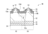
- FIG. 10 illustrates a cross-sectional configuration of a light receiving element (light receiving element 1B) according to Modification 2.
- the photoelectric conversion layer 12 and the plurality of contact layers 13 are provided in this order on the substrate 11 as in the above embodiment, and the plurality of contact layers 13 have gaps A on the photoelectric conversion layer 12. They are spaced apart.
- the first electrode 14 is electrically connected to each of the plurality of contact layers 13 through the opening H of the mask layer 19.
- a covering layer (covering layer 15B) and an insulating film 16 are formed in this order so as to cover a part of the surface (surface 12a) of the photoelectric conversion layer 12 and the side surface 13a of each contact layer 13.
- a diffusion region (diffusion region 17 ⁇ / b> B) containing impurities is formed in a region adjacent to the coating layer 15 ⁇ / b> B in the photoelectric conversion layer 12 and the contact layer 13.
- a second electrode 18 is formed on the surface of the substrate 11 opposite to the photoelectric conversion layer 12.
- the back surface of the second electrode 18 is a light incident surface S1.
- the coating layer 15B includes silicon germanium (SiGe) as a group IV semiconductor. Moreover, Si and Ge contained in the coating layer 15B are diffused into a part of the photoelectric conversion layer 12 and the contact layer 13 by the annealing treatment as described above, and a diffusion region 17B is formed. For this reason, the diffusion region 17B includes Si and Ge as n-type dopants in the photoelectric conversion layer 12, and forms a dense n-type region.
- SiGe silicon germanium
- the coating layer 15B containing the IV group semiconductor (SiGe) is in contact with the surface 12a of the photoelectric conversion layer 12, the interface defect density is reduced as compared with the case of being in contact with the insulating film. Further, a potential barrier is formed in the photoelectric conversion layer 12 by the diffusion region 17B. Therefore, an effect equivalent to that of the above embodiment can be obtained.
- SiGe has a lattice constant closer to that of compound semiconductors (InP and InGaAs) than Si, defects at the interface with the compound semiconductor can be further reduced.
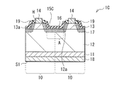
- FIG. 11 illustrates a cross-sectional configuration of a light receiving element (light receiving element 1 ⁇ / b> C) according to Modification 3.
- the photoelectric conversion layer 12 and the plurality of contact layers 13 are provided in this order on the substrate 11, and the plurality of contact layers 13 have gaps A on the photoelectric conversion layer 12, as in the above embodiment. They are spaced apart.
- the first electrode 14 is electrically connected to each of the plurality of contact layers 13 through the opening H of the mask layer 19.
- a covering layer (covering layer 15 ⁇ / b> C) and an insulating film 16 are formed in this order so as to cover a part of the surface (the face 12 a) of the photoelectric conversion layer 12 and the side face 13 a of each contact layer 13.
- a diffusion region 17 is formed adjacent to the cover layer 15C of the photoelectric conversion layer 12 and the contact layer 13, and Si contained in the cover layer 15C is diffused into the diffusion region 17.
- a second electrode 18 is formed on the surface of the substrate 11 opposite to the photoelectric conversion layer 12.
- the back surface of the second electrode 18 is a light incident surface S1.
- the covering layer 15C includes an n-type IV group semiconductor (including an IV group semiconductor and an element that functions as an n-type dopant for the group IV semiconductor).
- the coating layer 15C contains n-type Si (containing an element that functions as an n-type dopant with respect to Si and Si).
- the element that becomes an n-type dopant for Si include arsenic (As) and phosphorus (P).
- the coating layer 15 ⁇ / b> C containing the IV group semiconductor (n-type Si) is in contact with the surface 12 a of the photoelectric conversion layer 12, so that the interface defect density is reduced as compared with the case of being in contact with the insulating film.
- a potential barrier is formed in the photoelectric conversion layer 12 by the diffusion region 17. Therefore, an effect equivalent to that of the above embodiment can be obtained.
- the covering layer 15C contains the n-type dopant, the electron density in the IV group semiconductor in contact with the insulating film 16 is increased.
- the higher the electron density the lower the probability of interface recombination with the insulating film 16, so that the dark current reduction effect is improved.
- the n-type conversion near the interface between the IV group semiconductor and the compound semiconductor is strengthened, the potential barrier can be increased. Therefore, it is advantageous for suppressing crosstalk of signals between pixels.
- FIG. 12 illustrates a cross-sectional configuration of a light receiving element (light receiving element 1D) according to Modification 4.
- the photoelectric conversion layer 12 and the plurality of contact layers 13 are provided in this order on the substrate 11, and the plurality of contact layers 13 have gaps A on the photoelectric conversion layer 12. They are spaced apart.
- the first electrode 14 is electrically connected to each of the plurality of contact layers 13 through the opening H of the mask layer 19.
- a covering layer (covering layer 15 ⁇ / b> D) and an insulating film 16 are formed in this order so as to cover a part (surface 12 a) of the surface of the photoelectric conversion layer 12 and the side surface 13 a of each contact layer 13.
- a diffusion region (diffusion region 17 ⁇ / b> D) containing impurities is formed in a region adjacent to the coating layer 15 ⁇ / b> D in the photoelectric conversion layer 12 and the contact layer 13.
- a second electrode 18 is formed on the surface of the substrate 11 opposite to the photoelectric conversion layer 12.
- the back surface of the second electrode 18 is a light incident surface S1.
- the coating layer 15D includes an IV element semiconductor (for example, Si) and an impurity element that functions as an n-type dopant with respect to the compound semiconductor (the photoelectric conversion layer 12).
- an IV element semiconductor for example, Si
- an impurity element that functions as an n-type dopant with respect to the compound semiconductor (the photoelectric conversion layer 12).
- an element that functions as an n-type dopant for InGaAs for example, at least one of carbon (C), tin (Sn), lead (Pb), sulfur (S), tellurium (Te), and the like is included.
- C carbon
- tin (Sn) tin
- Pb lead
- Te tellurium
- the diffusion region 17D includes at least one of C, Sn, Pb, S, and Te as an n-type dopant, and forms a dense n-type region.
- the coating layer 15D containing the IV group semiconductor is in contact with the surface 12a of the photoelectric conversion layer 12, and therefore, the interface defect density is reduced as compared with the case of being in contact with the insulating film. Therefore, an effect equivalent to that of the above embodiment can be obtained.
- an element that functions as an n-type dopant including Si is diffused from the coating layer 15D. Therefore, an n-type region having a higher doping density can be formed in the diffusion region 17D, and a high potential barrier can be formed in the photoelectric conversion layer 12.
- FIG. 13 illustrates a cross-sectional configuration of a light receiving element (light receiving element 1E) according to Modification 5.
- FIG. 14 schematically shows a planar configuration of the light receiving element 1E.
- the light receiving element 1E has, for example, a photoelectric conversion layer 12 and a plurality of contact layers 13 in this order on the substrate 11 as in the above embodiment, and the plurality of contact layers 13 have gaps A on the photoelectric conversion layer 12. They are spaced apart.
- the first electrode 14 is electrically connected to each of the plurality of contact layers 13 through the opening H of the mask layer 19.
- a covering layer 15 and an insulating film 16 are formed in this order so as to cover part of the surface (surface 12 a) of the photoelectric conversion layer 12 and the side surface 13 a of each contact layer 13.
- a diffusion region 17 is formed in a region adjacent to the coating layer 15 in the photoelectric conversion layer 12 and the contact layer 13.
- a second electrode 18 is formed on the surface of the substrate 11 opposite to the photoelectric conversion layer 12.
- the back surface of the second electrode 18 is a light incident surface S1.
- a contact electrode (electrode 14A) that is electrically connected to the diffusion region 17 of the photoelectric conversion layer 12 is disposed.
- the electrode 14 ⁇ / b> A only needs to be electrically connected to the diffusion region 17, and may be formed at any position on the photoelectric conversion layer 12. Further, only one electrode 14A may be arranged with respect to the light receiving element 1E, or a plurality of electrodes 14A may be arranged.
- the coating layer 15 is in contact with the surface 12a of the photoelectric conversion layer 12, so that the interface defect density is reduced as compared with the case of being in contact with the insulating film. Further, a potential barrier is formed in the photoelectric conversion layer 12 by the diffusion region 17. Therefore, an effect equivalent to that of the above embodiment can be obtained.
- the potential of the diffusion region 17 can be controlled. For example, when a positive bias voltage is applied to the electrode 14A, the electron density near the surface 12a of the photoelectric conversion layer 12 can be increased.
- Such potential control using the electrode 14A makes it possible to reduce the interface recombination probability and at the same time enhance the electrical separation from adjacent pixels. Therefore, it becomes advantageous for suppression of dark current.
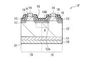
- FIG. 15 illustrates a cross-sectional configuration of a light receiving element (light receiving element 1F) according to Modification 6.
- the photoelectric conversion layer 12 and the plurality of contact layers 13 are provided in this order on the substrate 11, and the plurality of contact layers 13 have gaps A on the photoelectric conversion layer 12. They are spaced apart.
- the first electrode 14 is electrically connected to each of the plurality of contact layers 13 through the opening H of the mask layer 19.
- a covering layer 15 and insulating films (insulating films 16 and 16B) are formed in this order so as to cover a part of the surface (surface 12a) of the photoelectric conversion layer 12 and the side surface 13a of each contact layer 13.
- a diffusion region 17 is formed in a region adjacent to the coating layer 15 in the photoelectric conversion layer 12 and the contact layer 13.
- a second electrode 18 is formed on the surface of the substrate 11 opposite to the photoelectric conversion layer 12.
- the back surface of the second electrode 18 is a light incident surface S1.
- an insulating film 16B (second insulating film) is further laminated on the insulating film 16, and the insulating film 16B contains a positive fixed charge.
- the insulating film 16B containing such positive fixed charges can be formed by depositing SiN, SiO 2 , HfO 2 by, for example, CVD.
- the coating layer 15 is in contact with the surface 12a of the photoelectric conversion layer 12, so that the interface defect density is reduced as compared with the case of being in contact with the insulating film. Further, a potential barrier is formed in the photoelectric conversion layer 12 by the diffusion region 17. Therefore, an effect equivalent to that of the above embodiment can be obtained.
- the insulating film 16B containing a positive fixed charge is laminated on the covering layer 15, electrons are induced at the interface between the IV group semiconductor (covering layer 15) and the insulating film 16, and the interface generation recombination is performed. The effect of reducing the probability and improving the separability can be obtained.
- FIG. 16 illustrates a functional configuration of the imaging element 2 using the element structure of the light receiving element 1 (the same applies to the light receiving elements 1A to 1F) described in the above embodiments and the like.
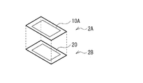
- the imaging element 2 is, for example, an infrared image sensor, and includes, for example, a pixel unit 10A and a circuit unit 20 that drives the pixel unit 10A.
- the circuit unit 20 includes, for example, a row scanning unit 131, a horizontal selection unit 133, a column scanning unit 134, and a system control unit 132.
- the pixel unit 10A has, for example, a plurality of pixels P that are two-dimensionally arranged in a matrix.
- pixel drive lines Lread for example, row selection lines and reset control lines
- vertical signal lines Lsig are wired to the pixel columns.
- the pixel drive line Lread transmits a drive signal for reading a signal from the pixel P.
- One end of the pixel drive line Lread is connected to an output end corresponding to each row of the row scanning unit 131.
- the row scanning unit 131 includes a shift register, an address decoder, and the like, and is a pixel driving unit that drives each pixel P of the pixel unit 10A in units of rows, for example.
- a signal output from each pixel P in the pixel row selected and scanned by the row scanning unit 131 is supplied to the horizontal selection unit 133 through each of the vertical signal lines Lsig.
- the horizontal selection unit 133 is configured by an amplifier, a horizontal selection switch, and the like provided for each vertical signal line Lsig.
- the column scanning unit 134 includes a shift register, an address decoder, and the like, and drives the horizontal selection switches in the horizontal selection unit 133 in order while scanning. By the selective scanning by the column scanning unit 134, the signal of each pixel transmitted through each of the vertical signal lines Lsig is sequentially output to the horizontal signal line 135 and is input to the signal processing unit (not shown) through the horizontal signal line 135.
- the signal processing unit not shown
- a substrate 2A having a pixel portion 10A and a substrate 2B having a circuit portion 20 are laminated.
- the configuration is not limited to this, and the circuit unit 20 may be formed on the same substrate as the pixel unit 10A, or may be provided in an external control IC.
- the circuit unit 20 may be formed on another substrate connected by a cable or the like.
- the system control unit 132 receives a clock given from the outside, data for instructing an operation mode, and the like, and outputs data such as internal information of the image sensor 2.
- the system control unit 132 further includes a timing generator that generates various timing signals.
- the row scanning unit 131, the horizontal selection unit 133, the column scanning unit 134, and the like are based on the various timing signals generated by the timing generator. Drive control is performed.
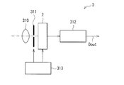
- FIG. 18 shows a schematic configuration of an electronic apparatus 3 (camera) as an example.
- the electronic device 3 is a camera capable of taking a still image or a moving image, for example. 313 and a signal processing unit 312.
- the optical system 310 guides image light (incident light) from the subject to the image sensor 2.
- the optical system 310 may be composed of a plurality of optical lenses.
- the shutter device 311 controls the light irradiation period and the light shielding period to the image sensor 2.
- the drive unit 313 controls the transfer operation of the image sensor 2 and the shutter operation of the shutter device 311.
- the signal processing unit 312 performs various signal processing on the signal output from the image sensor 2.
- the video signal Dout after the signal processing is stored in a storage medium such as a memory, or is output to a monitor or the like.
- the layer configuration of the light receiving element described in the above embodiment is an example, and other layers may be provided.
- the material and thickness of each layer are examples, and are not limited to those described above.
- the contact layer 13 contains a p-type compound semiconductor and the photoelectric converting layer 12 contains an n-type compound semiconductor was illustrated, the conductivity type of the contact layer 13 and the photoelectric converting layer 12 Is not limited to this.
- the contact layer 13 may include an n-type compound semiconductor, or the photoelectric conversion layer 12 may include a p-type compound semiconductor.
- the present disclosure may be configured as follows.
- a photoelectric conversion layer that includes the first compound semiconductor and absorbs wavelengths in the infrared region to generate charges;
- a light receiving element comprising: a covering layer including a group IV semiconductor formed so as to cover a portion of the surface of the photoelectric conversion layer corresponding to the gap and a side surface of each contact layer.
- the coating layer includes germanium; The light receiving element according to (8) or (9), wherein the first insulating film is formed on the coating layer via an insulating film containing germanium oxide (GeO 2 ).
- the photoelectric conversion layer is an n-type having a doping density of 1.0 ⁇ 10 18 cm ⁇ 3 or less, or a p-type having a doping density of 1.0 ⁇ 10 16 cm ⁇ 3 or less (1) to (13) The light receiving element as described in any one of.
- the photoelectric conversion layer and the contact layer are provided in this order, A first electrode electrically connected to the contact layer;
- the light receiving element according to any one of (1) to (14), further comprising: a second electrode electrically connected to the substrate.
- (16) Forming a photoelectric conversion layer that includes the first compound semiconductor and generates charges by absorbing wavelengths in the infrared region; Forming a plurality of contact layers including a second compound semiconductor and spaced apart from each other on the photoelectric conversion layer; A method for manufacturing a light receiving element, wherein a covering layer including a group IV semiconductor is formed so as to cover a portion of the surface of the photoelectric conversion layer corresponding to the gap and a side surface of each contact layer.
- the gap between the plurality of contact layers is formed by etching.
- the diffusion region in which an element contained in the coating layer is diffused is formed in a selective region adjacent to the coating layer in the photoelectric conversion layer and the contact layer.
- a photoelectric conversion layer that includes the first compound semiconductor and absorbs wavelengths in the infrared region to generate charges;
- a plurality of contact layers including a second compound semiconductor and spaced apart from each other on the photoelectric conversion layer and provided for each of the pixels;
- An imaging device comprising: a covering layer including a group IV semiconductor and a portion corresponding to the gap in a surface of the photoelectric conversion layer and a side surface of each contact layer.
- a photoelectric conversion layer that includes the first compound semiconductor and absorbs wavelengths in the infrared region to generate charges;
- An electronic apparatus having an imaging element comprising: a covering layer including a group IV semiconductor formed on the surface of the photoelectric conversion layer so as to cover a portion corresponding to the gap and a side surface of each contact layer.
Landscapes
- Engineering & Computer Science (AREA)
- Multimedia (AREA)
- Signal Processing (AREA)
- Light Receiving Elements (AREA)
- Solid State Image Pick-Up Elements (AREA)
- Chemical & Material Sciences (AREA)
- Inorganic Chemistry (AREA)
Abstract
Description
1.実施の形態(光電変換層の表面とコンタクト層の側面とを覆ってIV族半導体(Si)を含む被覆層を有する受光素子の例)
2.変形例1(他のIV族半導体(Ge)を含む被覆層を有する受光素子の例)
3.変形例3(他のIV族半導体(SiGe)を含む被覆層を有する受光素子の例)
4.変形例4(n型Siから構成された被覆層を有する受光素子の例)
5.変形例5(光電変換層においてn型として機能する不純物元素を含む被覆層を有する受光素子の例)
6.変形例6(光電変換層の拡散領域を電位制御するための電極を備えた受光素子の例)7.変形例7(被覆層の上に固定電荷を含む絶縁膜を有する受光素子の例)
8.適用例1(撮像素子の例)
9.適用例2(電子機器の例)
[構成]
図1は、本開示の一実施形態の受光素子(受光素子1)の断面構成を表したものである。図2は、受光素子1の平面構成を模式的に表したものである。受光素子1は、例えば化合物半導体を用いた赤外線センサ等に適用されるものであり、例えば2次元配置された複数の受光単位領域としての画素10(後述の撮像素子の画素Pに対応)を含んでいる。尚、図1では、2つの画素Pに相当する部分の断面構成について示している。
受光素子1は、例えば次のようにして製造することができる。図3A~図4Cは、受光素子1の要部の製造工程を工程順に示したものである。
本実施の形態の受光素子1では、第2電極18および基板11を介して、光電変換層12へ赤外線IRが入射すると、この赤外線IRが光電変換層12において吸収される。これにより、光電変換層12では、正孔(ホール)および電子の対が発生する(光電変換される)。このとき、例えば第1電極14と第2電極18とを通じて光電変換層12に所定の電圧が印加される(電位勾配が形成される)ことで、発生した電荷のうちの一方の電荷(ここでは、正孔)が、信号電荷として第1電極14の側へ収集される。この信号電荷は、第1電極14を通じて、図示しない画素回路によって読み出される。
図9は、変形例1に係る受光素子(受光素子1A)の断面構成を表したものである。受光素子1Aでは、上記実施の形態と同様、基板11上に、例えば光電変換層12と複数のコンタクト層13とをこの順に有し、光電変換層12上において複数のコンタクト層13が間隙Aを隔てて配置されている。複数のコンタクト層13のそれぞれには、第1電極14が、マスク層19の開口Hを介して電気的に接続されている。光電変換層12の表面の一部(面12a)と各コンタクト層13の側面13aとを覆うように、被覆層(被覆層15A)と絶縁膜(絶縁膜16A,16)とがこの順に形成されている。光電変換層12およびコンタクト層13のうちの被覆層15Aに隣接する領域には、不純物を含む拡散領域(拡散領域17A)が形成されている。基板11の光電変換層12と反対側の面には、例えば第2電極18が形成されている。この受光素子1では、例えば第2電極18の裏面が光入射面S1となっている。
図10は、変形例2に係る受光素子(受光素子1B)の断面構成を表したものである。受光素子1Bでは、上記実施の形態と同様、基板11上に、例えば光電変換層12と複数のコンタクト層13とをこの順に有し、光電変換層12上において複数のコンタクト層13が間隙Aを隔てて配置されている。複数のコンタクト層13のそれぞれには、第1電極14が、マスク層19の開口Hを介して電気的に接続されている。光電変換層12の表面の一部(面12a)と各コンタクト層13の側面13aとを覆うように、被覆層(被覆層15B)と絶縁膜16とがこの順に形成されている。光電変換層12およびコンタクト層13のうちの被覆層15Bに隣接する領域には、不純物を含む拡散領域(拡散領域17B)が形成されている。基板11の光電変換層12と反対側の面には、例えば第2電極18が形成されている。この受光素子1では、例えば第2電極18の裏面が光入射面S1となっている。
図11は、変形例3に係る受光素子(受光素子1C)の断面構成を表したものである。受光素子1Cでは、上記実施の形態と同様、基板11上に、例えば光電変換層12と複数のコンタクト層13とをこの順に有し、光電変換層12上において複数のコンタクト層13が間隙Aを隔てて配置されている。複数のコンタクト層13のそれぞれには、第1電極14が、マスク層19の開口Hを介して電気的に接続されている。光電変換層12の表面の一部(面12a)と各コンタクト層13の側面13aとを覆うように、被覆層(被覆層15C)と絶縁膜16とがこの順に形成されている。光電変換層12およびコンタクト層13のうちの被覆層15Cに隣接して、拡散領域17が形成され、この拡散領域17には、被覆層15Cに含まれるSiが拡散されている。基板11の光電変換層12と反対側の面には、例えば第2電極18が形成されている。この受光素子1では、例えば第2電極18の裏面が光入射面S1となっている。
図12は、変形例4に係る受光素子(受光素子1D)の断面構成を表したものである。受光素子1Dでは、上記実施の形態と同様、基板11上に、例えば光電変換層12と複数のコンタクト層13とをこの順に有し、光電変換層12上において複数のコンタクト層13が間隙Aを隔てて配置されている。複数のコンタクト層13のそれぞれには、第1電極14が、マスク層19の開口Hを介して電気的に接続されている。光電変換層12の表面の一部(面12a)と各コンタクト層13の側面13aとを覆うように、被覆層(被覆層15D)と絶縁膜16とがこの順に形成されている。光電変換層12およびコンタクト層13のうちの被覆層15Dに隣接する領域には、不純物を含む拡散領域(拡散領域17D)が形成されている。基板11の光電変換層12と反対側の面には、例えば第2電極18が形成されている。この受光素子1では、例えば第2電極18の裏面が光入射面S1となっている。
図13は、変形例5に係る受光素子(受光素子1E)の断面構成を表したものである。図14は、受光素子1Eの平面構成を模式的に表したものである。受光素子1Eでは、上記実施の形態と同様、基板11上に、例えば光電変換層12と複数のコンタクト層13とをこの順に有し、光電変換層12上において複数のコンタクト層13が間隙Aを隔てて配置されている。複数のコンタクト層13のそれぞれには、第1電極14が、マスク層19の開口Hを介して電気的に接続されている。光電変換層12の表面の一部(面12a)と各コンタクト層13の側面13aとを覆うように、被覆層15と絶縁膜16とがこの順に形成されている。光電変換層12およびコンタクト層13のうちの被覆層15に隣接する領域には、拡散領域17が形成されている。基板11の光電変換層12と反対側の面には、例えば第2電極18が形成されている。この受光素子1では、例えば第2電極18の裏面が光入射面S1となっている。
ことから、絶縁膜と接する場合に比べ、界面欠陥密度が低減される。また、拡散領域17により、光電変換層12内にはポテンシャル障壁が形成される。よって、上記実施の形態と同等の効果を得ることができる。
図15は、変形例6に係る受光素子(受光素子1F)の断面構成を表したものである。受光素子1Fでは、上記実施の形態と同様、基板11上に、例えば光電変換層12と複数のコンタクト層13とをこの順に有し、光電変換層12上において複数のコンタクト層13が間隙Aを隔てて配置されている。複数のコンタクト層13のそれぞれには、第1電極14が、マスク層19の開口Hを介して電気的に接続されている。光電変換層12の表面の一部(面12a)と各コンタクト層13の側面13aとを覆うように、被覆層15と絶縁膜(絶縁膜16,16B)とがこの順に形成されている。光電変換層12およびコンタクト層13のうちの被覆層15に隣接する領域には、拡散領域17が形成されている。基板11の光電変換層12と反対側の面には、例えば第2電極18が形成されている。この受光素子1では、例えば第2電極18の裏面が光入射面S1となっている。
図16は、上記実施の形態等において説明した受光素子1(受光素子1A~1Fも同様)の素子構造を用いた撮像素子2の機能構成を表したものである。撮像素子2は、例えば赤外線イメージセンサであり、例えば画素部10Aと、この画素部10Aを駆動する回路部20とを有している。回路部20は、例えば行走査部131、水平選択部133、列走査部134およびシステム制御部132を有している。
上述の撮像素子2は、例えば赤外領域を撮像可能なカメラなど、様々なタイプの電子機器に適用することができる。図18に、その一例として、電子機器3(カメラ)の概略構成を示す。この電子機器3は、例えば静止画または動画を撮影可能なカメラであり、撮像素子2と、光学系(光学レンズ)310と、シャッタ装置311と、撮像素子2およびシャッタ装置311を駆動する駆動部313と、信号処理部312とを有する。
(1)
第1の化合物半導体を含むと共に、赤外領域の波長を吸収して電荷を発生する光電変換層と、
第2の化合物半導体を含むと共に、前記光電変換層上に互いに間隙を隔てて設けられた複数のコンタクト層と、
前記光電変換層の表面のうちの前記間隙に対応する部分と各コンタクト層の側面とを覆って形成されると共に、IV族半導体を含む被覆層と
を備えた
受光素子。
(2)
前記被覆層は、シリコン(Si)またはゲルマニウム(Ge)を含む
上記(1)に記載の受光素子。
(3)
前記被覆層は、シリコンゲルマニウム(SiGe)を含む
上記(1)または(2)に記載の受光素子。
(4)
前記被覆層は、前記IV族半導体と、前記IV族半導体に対してn型のドーパントとして機能する元素とを含む
上記(1)~(3)のいずれか1つに記載の受光素子。
(5)
前記被覆層は、前記IV族半導体と、前記光電変換層に対してn型のドーパントとして機能する元素とを含む
上記(1)~(4)のいずれか1つに記載の受光素子。
(6)
前記光電変換層および前記コンタクト層のうちの前記被覆層に隣接する選択的な領域に、前記被覆層に含まれる元素が拡散された拡散領域を有する
上記(1)~(5)のいずれか1つに記載の受光素子。
(7)
前記光電変換層の前記拡散領域に電気的に接続されたコンタクト電極を更に備えた
上記(6)に記載の受光素子。
(8)
前記被覆層上に第1の絶縁膜を更に備えた
上記(1)~(7)のいずれか1つに記載の受光素子。
(9)
前記第1の絶縁膜は、シリコン(Si)、窒素(N)、アルミニウム(Al)およびハフニウム(Hf)のうちのいずれかを含む
上記(8)に記載の受光素子。
(10)
前記被覆層はゲルマニウムを含み、
前記被覆層上に、酸化ゲルマニウム(GeO2)を含む絶縁膜を介して、前記第1の絶縁膜が形成された
上記(8)または(9)に記載の受光素子。
(11)
前記第1の絶縁膜上に、正の固定電荷を含む第2の絶縁膜を更に備えた
上記(8)~(10)のいずれか1つに記載の受光素子。
(12)
前記第1および第2の化合物半導体はIII-V族半導体である
上記(1)~(11)のいずれか1つに記載の受光素子。
(13)
前記被覆層の厚みは、0.25nm以上100nm以下である
上記(1)~(12)のいずれか1つに記載の受光素子。
(14)
前記光電変換層は、ドーピング密度が1.0×1018cm-3以下のn型、またはドーピング密度が1.0×1016cm-3以下のp型である
上記(1)~(13)のいずれか1つに記載の受光素子。
(15)
基板上に、前記光電変換層と前記コンタクト層とがこの順に設けられ、
前記コンタクト層に電気的に接続された第1電極と、
前記基板に電気的に接続された第2電極と
を更に備えた
上記(1)~(14)のいずれか1つに記載の受光素子。
(16)
第1の化合物半導体を含むと共に、赤外領域の波長を吸収して電荷を発生する光電変換層を形成し、
第2の化合物半導体を含むと共に前記光電変換層上に互いに間隙を隔てて配置された複数のコンタクト層を形成し、
前記光電変換層の表面のうちの前記間隙に対応する部分と各コンタクト層の側面とを覆って、IV族半導体を含む被覆層を形成する
受光素子の製造方法。
(17)
前記複数のコンタクト層の前記間隙を、エッチングにより形成する
上記(16)に記載の受光素子の製造方法。
(18)
前記被覆層を形成した後にアニール処理を施すことにより、
前記光電変換層および前記コンタクト層のうちの前記被覆層に隣接する選択的な領域に、前記被覆層に含まれる元素が拡散された拡散領域を形成する
上記(16)または(17)に記載の受光素子の製造方法。
(19)
複数の画素を含み、
第1の化合物半導体を含むと共に、赤外領域の波長を吸収して電荷を発生する光電変換層と、
第2の化合物半導体を含むと共に、前記光電変換層上に互いに間隙を隔てて、かつ前記画素毎に設けられた複数のコンタクト層と、
前記光電変換層の表面のうちの前記間隙に対応する部分と各コンタクト層の側面とを覆って形成されると共に、IV族半導体を含む被覆層と
を備えた
撮像素子。
(20)
複数の画素を含み、
第1の化合物半導体を含むと共に、赤外領域の波長を吸収して電荷を発生する光電変換層と、
第2の化合物半導体を含むと共に、前記光電変換層上に互いに間隙を隔てて、かつ前記画素毎に設けられた複数のコンタクト層と、
前記光電変換層の表面のうちの前記間隙に対応する部分と各コンタクト層の側面とを覆って形成されると共に、IV族半導体を含む被覆層と
を備えた
撮像素子を有する電子機器。
Claims (20)
- 第1の化合物半導体を含むと共に、赤外領域の波長を吸収して電荷を発生する光電変換層と、
第2の化合物半導体を含むと共に、前記光電変換層上に互いに間隙を隔てて設けられた複数のコンタクト層と、
前記光電変換層の表面のうちの前記間隙に対応する部分と各コンタクト層の側面とを覆って形成されると共に、IV族半導体を含む被覆層と
を備えた
受光素子。 - 前記被覆層は、シリコン(Si)またはゲルマニウム(Ge)を含む
請求項1に記載の受光素子。 - 前記被覆層は、シリコンゲルマニウム(SiGe)を含む
請求項1に記載の受光素子。 - 前記被覆層は、前記IV族半導体と、前記IV族半導体に対してn型のドーパントとして機能する元素とを含む
請求項1に記載の受光素子。 - 前記被覆層は、前記IV族半導体と、前記光電変換層に対してn型のドーパントとして機能する元素とを含む
請求項1に記載の受光素子。 - 前記光電変換層および前記コンタクト層のうちの前記被覆層に隣接する選択的な領域に、前記被覆層に含まれる元素が拡散された拡散領域を有する
請求項1に記載の受光素子。 - 前記光電変換層の前記拡散領域に電気的に接続されたコンタクト電極を更に備えた
請求項6に記載の受光素子。 - 前記被覆層上に第1の絶縁膜を更に備えた
請求項1に記載の受光素子。 - 前記第1の絶縁膜は、シリコン(Si)、窒素(N)、アルミニウム(Al)およびハフニウム(Hf)のうちのいずれかを含む
請求項8に記載の受光素子。 - 前記被覆層はゲルマニウムを含み、
前記被覆層上に、酸化ゲルマニウム(GeO2)を含む絶縁膜を介して、前記第1の絶縁膜が形成された
請求項8に記載の受光素子。 - 前記第1の絶縁膜上に、正の固定電荷を含む第2の絶縁膜を更に備えた
請求項8に記載の受光素子。 - 前記第1および第2の化合物半導体はIII-V族半導体である
請求項1に記載の受光素子。 - 前記被覆層の厚みは、0.25nm以上100nm以下である
請求項1に記載の受光素子。 - 前記光電変換層は、ドーピング密度が1.0×1018cm-3以下のn型、またはドーピング密度が1.0×1016cm-3以下のp型である
請求項1に記載の受光素子。 - 基板上に、前記光電変換層と前記コンタクト層とがこの順に設けられ、
前記コンタクト層に電気的に接続された第1電極と、
前記基板に電気的に接続された第2電極と
を更に備えた
請求項1に記載の受光素子。 - 第1の化合物半導体を含むと共に、赤外領域の波長を吸収して電荷を発生する光電変換層を形成し、
第2の化合物半導体を含むと共に前記光電変換層上に互いに間隙を隔てて配置された複数のコンタクト層を形成し、
前記光電変換層の表面のうちの前記間隙に対応する部分と各コンタクト層の側面とを覆って、IV族半導体を含む被覆層を形成する
受光素子の製造方法。 - 前記複数のコンタクト層の前記間隙を、エッチングにより形成する
請求項16に記載の受光素子の製造方法。 - 前記被覆層を形成した後にアニール処理を施すことにより、
前記光電変換層および前記コンタクト層のうちの前記被覆層に隣接する選択的な領域に、前記被覆層に含まれる元素が拡散された拡散領域を形成する
請求項16に記載の受光素子の製造方法。 - 複数の画素を含み、
第1の化合物半導体を含むと共に、赤外領域の波長を吸収して電荷を発生する光電変換層と、
第2の化合物半導体を含むと共に、前記光電変換層上に互いに間隙を隔てて、かつ前記画素毎に設けられた複数のコンタクト層と、
前記光電変換層の表面のうちの前記間隙に対応する部分と各コンタクト層の側面とを覆って形成されると共に、IV族半導体を含む被覆層と
を備えた
撮像素子。 - 複数の画素を含み、
第1の化合物半導体を含むと共に、赤外領域の波長を吸収して電荷を発生する光電変換層と、
第2の化合物半導体を含むと共に、前記光電変換層上に互いに間隙を隔てて、かつ前記画素毎に設けられた複数のコンタクト層と、
前記光電変換層の表面のうちの前記間隙に対応する部分と各コンタクト層の側面とを覆って形成されると共に、IV族半導体を含む被覆層と
を備えた
撮像素子を有する電子機器。
Priority Applications (5)
| Application Number | Priority Date | Filing Date | Title |
|---|---|---|---|
| JP2017562447A JP6763406B2 (ja) | 2016-01-20 | 2016-11-15 | 受光素子、受光素子の製造方法、撮像素子および電子機器 |
| US16/069,272 US10622392B2 (en) | 2016-01-20 | 2016-11-15 | Light receiving device, method of manufacturing light receiving device, imaging device, and electronic apparatus |
| EP16886443.7A EP3407392B1 (en) | 2016-01-20 | 2016-11-15 | Light receiving element, method for manufacturing light receiving element, image pickup element, and electronic apparatus |
| CN201680074813.2A CN108369967B (zh) | 2016-01-20 | 2016-11-15 | 光接收元件、光接收元件的制造方法、成像元件和电子设备 |
| US16/805,275 US11205668B2 (en) | 2016-01-20 | 2020-02-28 | Light receiving device, method of manufacturing light receiving device, imaging device, and electronic apparatus |
Applications Claiming Priority (2)
| Application Number | Priority Date | Filing Date | Title |
|---|---|---|---|
| JP2016-008460 | 2016-01-20 | ||
| JP2016008460 | 2016-01-20 |
Related Child Applications (2)
| Application Number | Title | Priority Date | Filing Date |
|---|---|---|---|
| US16/069,272 A-371-Of-International US10622392B2 (en) | 2016-01-20 | 2016-11-15 | Light receiving device, method of manufacturing light receiving device, imaging device, and electronic apparatus |
| US16/805,275 Division US11205668B2 (en) | 2016-01-20 | 2020-02-28 | Light receiving device, method of manufacturing light receiving device, imaging device, and electronic apparatus |
Publications (1)
| Publication Number | Publication Date |
|---|---|
| WO2017126204A1 true WO2017126204A1 (ja) | 2017-07-27 |
Family
ID=59362715
Family Applications (1)
| Application Number | Title | Priority Date | Filing Date |
|---|---|---|---|
| PCT/JP2016/083857 Ceased WO2017126204A1 (ja) | 2016-01-20 | 2016-11-15 | 受光素子、受光素子の製造方法、撮像素子および電子機器 |
Country Status (5)
| Country | Link |
|---|---|
| US (2) | US10622392B2 (ja) |
| EP (1) | EP3407392B1 (ja) |
| JP (1) | JP6763406B2 (ja) |
| CN (1) | CN108369967B (ja) |
| WO (1) | WO2017126204A1 (ja) |
Cited By (4)
| Publication number | Priority date | Publication date | Assignee | Title |
|---|---|---|---|---|
| CN110767666A (zh) * | 2018-07-27 | 2020-02-07 | 台湾积体电路制造股份有限公司 | 覆盖结构、半导体器件及其形成方法 |
| WO2021084983A1 (ja) * | 2019-10-30 | 2021-05-06 | ソニーセミコンダクタソリューションズ株式会社 | 受光素子、受光素子の製造方法及び固体撮像装置 |
| WO2021149500A1 (ja) * | 2020-01-20 | 2021-07-29 | ソニーセミコンダクタソリューションズ株式会社 | 光電変換装置の製造方法、及び光電変換装置 |
| WO2022149362A1 (ja) * | 2021-01-08 | 2022-07-14 | ソニーセミコンダクタソリューションズ株式会社 | 固体撮像装置及び電子機器 |
Families Citing this family (2)
| Publication number | Priority date | Publication date | Assignee | Title |
|---|---|---|---|---|
| FR3092700B1 (fr) * | 2019-02-07 | 2021-01-22 | Commissariat Energie Atomique | Matrice de photo-détecteurs à barrière avec pixellisation par déplétions locales |
| US20240305906A1 (en) * | 2021-03-22 | 2024-09-12 | Sony Semiconductor Solutions Corporation | Solid-state imaging element and manufacturing method thereof |
Citations (6)
| Publication number | Priority date | Publication date | Assignee | Title |
|---|---|---|---|---|
| JP2003023173A (ja) * | 2001-07-06 | 2003-01-24 | Sumitomo Electric Ind Ltd | pin型受光素子 |
| US20080111152A1 (en) * | 2006-11-14 | 2008-05-15 | Lockheed Martin Corporation | Sub-pixel nbn detector |
| JP2010056173A (ja) * | 2008-08-26 | 2010-03-11 | Opnext Japan Inc | 裏面入射型受光素子およびその製造方法 |
| JP2013093385A (ja) * | 2011-10-24 | 2013-05-16 | Sumitomo Electric Ind Ltd | 受光素子、およびその製造方法 |
| JP2013140854A (ja) * | 2011-12-28 | 2013-07-18 | Seiko Epson Corp | 光伝導アンテナ、テラヘルツ波発生装置、カメラ、イメージング装置および計測装置 |
| JP2014127499A (ja) * | 2012-12-25 | 2014-07-07 | Sumitomo Electric Ind Ltd | 受光デバイス、その製造法、およびセンシング装置 |
Family Cites Families (9)
| Publication number | Priority date | Publication date | Assignee | Title |
|---|---|---|---|---|
| US7429496B2 (en) * | 2005-08-30 | 2008-09-30 | Taiwan Semiconductor Manufacturing Co., Ltd. | Buried photodiode for image sensor with shallow trench isolation technology |
| JP2007243100A (ja) * | 2006-03-13 | 2007-09-20 | Iwate Toshiba Electronics Co Ltd | 固体撮像装置およびその製造方法 |
| US7687871B2 (en) * | 2006-03-19 | 2010-03-30 | Shimon Maimon | Reduced dark current photodetector |
| US8502271B2 (en) * | 2009-10-23 | 2013-08-06 | Lockheed Martin Corporation | Barrier photodetector with planar top layer |
| CN101783345A (zh) * | 2010-03-04 | 2010-07-21 | 无锡新洁能功率半导体有限公司 | 一种沟槽型半导体整流器及其制造方法 |
| EP2822270A1 (en) * | 2012-02-27 | 2015-01-07 | Sony Corporation | Imaging element and electronic equipment |
| CN103378236B (zh) * | 2012-04-25 | 2017-04-05 | 清华大学 | 具有微构造的外延结构体 |
| CN104078478B (zh) * | 2014-07-04 | 2017-10-27 | 豪威科技(上海)有限公司 | 背照式cmos影像传感器及其制造方法 |
| JP2016219587A (ja) * | 2015-05-20 | 2016-12-22 | ソニー株式会社 | 半導体光デバイス |
-
2016
- 2016-11-15 EP EP16886443.7A patent/EP3407392B1/en active Active
- 2016-11-15 JP JP2017562447A patent/JP6763406B2/ja active Active
- 2016-11-15 WO PCT/JP2016/083857 patent/WO2017126204A1/ja not_active Ceased
- 2016-11-15 US US16/069,272 patent/US10622392B2/en active Active
- 2016-11-15 CN CN201680074813.2A patent/CN108369967B/zh active Active
-
2020
- 2020-02-28 US US16/805,275 patent/US11205668B2/en active Active
Patent Citations (6)
| Publication number | Priority date | Publication date | Assignee | Title |
|---|---|---|---|---|
| JP2003023173A (ja) * | 2001-07-06 | 2003-01-24 | Sumitomo Electric Ind Ltd | pin型受光素子 |
| US20080111152A1 (en) * | 2006-11-14 | 2008-05-15 | Lockheed Martin Corporation | Sub-pixel nbn detector |
| JP2010056173A (ja) * | 2008-08-26 | 2010-03-11 | Opnext Japan Inc | 裏面入射型受光素子およびその製造方法 |
| JP2013093385A (ja) * | 2011-10-24 | 2013-05-16 | Sumitomo Electric Ind Ltd | 受光素子、およびその製造方法 |
| JP2013140854A (ja) * | 2011-12-28 | 2013-07-18 | Seiko Epson Corp | 光伝導アンテナ、テラヘルツ波発生装置、カメラ、イメージング装置および計測装置 |
| JP2014127499A (ja) * | 2012-12-25 | 2014-07-07 | Sumitomo Electric Ind Ltd | 受光デバイス、その製造法、およびセンシング装置 |
Non-Patent Citations (1)
| Title |
|---|
| See also references of EP3407392A4 * |
Cited By (10)
| Publication number | Priority date | Publication date | Assignee | Title |
|---|---|---|---|---|
| CN110767666A (zh) * | 2018-07-27 | 2020-02-07 | 台湾积体电路制造股份有限公司 | 覆盖结构、半导体器件及其形成方法 |
| CN110767666B (zh) * | 2018-07-27 | 2022-04-26 | 台湾积体电路制造股份有限公司 | 覆盖结构、半导体器件及其形成方法 |
| WO2021084983A1 (ja) * | 2019-10-30 | 2021-05-06 | ソニーセミコンダクタソリューションズ株式会社 | 受光素子、受光素子の製造方法及び固体撮像装置 |
| JPWO2021084983A1 (ja) * | 2019-10-30 | 2021-05-06 | ||
| JP7561752B2 (ja) | 2019-10-30 | 2024-10-04 | ソニーセミコンダクタソリューションズ株式会社 | 受光素子、受光素子の製造方法及び固体撮像装置 |
| WO2021149500A1 (ja) * | 2020-01-20 | 2021-07-29 | ソニーセミコンダクタソリューションズ株式会社 | 光電変換装置の製造方法、及び光電変換装置 |
| JPWO2021149500A1 (ja) * | 2020-01-20 | 2021-07-29 | ||
| US20230036227A1 (en) * | 2020-01-20 | 2023-02-02 | Sony Semiconductor Solutions Corporation | Method of manufacturing photoelectric conversion device, and photoelectric conversion device |
| JP7642569B2 (ja) | 2020-01-20 | 2025-03-10 | ソニーセミコンダクタソリューションズ株式会社 | 光電変換装置の製造方法、及び光電変換装置 |
| WO2022149362A1 (ja) * | 2021-01-08 | 2022-07-14 | ソニーセミコンダクタソリューションズ株式会社 | 固体撮像装置及び電子機器 |
Also Published As
| Publication number | Publication date |
|---|---|
| US11205668B2 (en) | 2021-12-21 |
| US20190019830A1 (en) | 2019-01-17 |
| JP6763406B2 (ja) | 2020-09-30 |
| US10622392B2 (en) | 2020-04-14 |
| CN108369967A (zh) | 2018-08-03 |
| US20200203411A1 (en) | 2020-06-25 |
| JPWO2017126204A1 (ja) | 2018-11-15 |
| EP3407392B1 (en) | 2020-07-08 |
| EP3407392A4 (en) | 2019-01-23 |
| EP3407392A1 (en) | 2018-11-28 |
| CN108369967B (zh) | 2021-12-14 |
Similar Documents
| Publication | Publication Date | Title |
|---|---|---|
| US10903257B2 (en) | Solid-state imaging device, driving method for solid-state imaging device, and electronic appliance | |
| US11205668B2 (en) | Light receiving device, method of manufacturing light receiving device, imaging device, and electronic apparatus | |
| JP4992446B2 (ja) | 固体撮像装置及びその製造方法、並びにカメラ | |
| US8669135B2 (en) | System and method for fabricating a 3D image sensor structure | |
| TWI463647B (zh) | 固態成像裝置及其製造方法,及成像設備 | |
| JP6186205B2 (ja) | 撮像素子および撮像装置 | |
| US20120080726A1 (en) | Solid-state imaging device, method of manufacturing the same, and electronic device | |
| KR20180008327A (ko) | 이중 대역 광검출기 및 이의 제작 방법 | |
| US9893101B2 (en) | Solid-state image pickup unit, method of manufacturing solid-state image pickup unit, and electronic apparatus | |
| US9257464B2 (en) | Solid-state image device, method of fabricating the same, and electronic apparatus | |
| US10943932B2 (en) | Light-receiving element, method of manufacturing light-receiving element, imaging device, and electronic apparatus | |
| TWI416716B (zh) | 固態影像裝置,其製造方法,及攝像設備 | |
| JP2009283603A (ja) | 検出装置、受光素子アレイおよびその製造方法 | |
| US20190051682A1 (en) | Solid-state imaging device and method of manufacturing the same | |
| JP7516730B2 (ja) | 赤外線センサおよび光検出方法 | |
| KR20170040468A (ko) | 이미지 센서 및 그 제조방법 |
Legal Events
| Date | Code | Title | Description |
|---|---|---|---|
| 121 | Ep: the epo has been informed by wipo that ep was designated in this application |
Ref document number: 16886443 Country of ref document: EP Kind code of ref document: A1 |
|
| ENP | Entry into the national phase |
Ref document number: 2017562447 Country of ref document: JP Kind code of ref document: A |
|
| NENP | Non-entry into the national phase |
Ref country code: DE |
|
| WWE | Wipo information: entry into national phase |
Ref document number: 2016886443 Country of ref document: EP |
|
| ENP | Entry into the national phase |
Ref document number: 2016886443 Country of ref document: EP Effective date: 20180820 |