WO2017126606A1 - パッケージ用基板、およびその製造方法 - Google Patents
パッケージ用基板、およびその製造方法 Download PDFInfo
- Publication number
- WO2017126606A1 WO2017126606A1 PCT/JP2017/001744 JP2017001744W WO2017126606A1 WO 2017126606 A1 WO2017126606 A1 WO 2017126606A1 JP 2017001744 W JP2017001744 W JP 2017001744W WO 2017126606 A1 WO2017126606 A1 WO 2017126606A1
- Authority
- WO
- WIPO (PCT)
- Prior art keywords
- substrate
- insulating layer
- core substrate
- layer
- wiring
- Prior art date
- Legal status (The legal status is an assumption and is not a legal conclusion. Google has not performed a legal analysis and makes no representation as to the accuracy of the status listed.)
- Ceased
Links
Images


Classifications
-
- H—ELECTRICITY
- H05—ELECTRIC TECHNIQUES NOT OTHERWISE PROVIDED FOR
- H05K—PRINTED CIRCUITS; CASINGS OR CONSTRUCTIONAL DETAILS OF ELECTRIC APPARATUS; MANUFACTURE OF ASSEMBLAGES OF ELECTRICAL COMPONENTS
- H05K3/00—Apparatus or processes for manufacturing printed circuits
- H05K3/0011—Working of insulating substrates or insulating layers
- H05K3/0044—Mechanical working of the substrate, e.g. drilling or punching
- H05K3/0052—Depaneling, i.e. dividing a panel into circuit boards; Working of the edges of circuit boards
-
- H—ELECTRICITY
- H10—SEMICONDUCTOR DEVICES; ELECTRIC SOLID-STATE DEVICES NOT OTHERWISE PROVIDED FOR
- H10W—GENERIC PACKAGES, INTERCONNECTIONS, CONNECTORS OR OTHER CONSTRUCTIONAL DETAILS OF DEVICES COVERED BY CLASS H10
- H10W70/00—Package substrates; Interposers; Redistribution layers [RDL]
- H10W70/60—Insulating or insulated package substrates; Interposers; Redistribution layers
- H10W70/62—Insulating or insulated package substrates; Interposers; Redistribution layers characterised by their interconnections
- H10W70/65—Shapes or dispositions of interconnections
-
- H—ELECTRICITY
- H10—SEMICONDUCTOR DEVICES; ELECTRIC SOLID-STATE DEVICES NOT OTHERWISE PROVIDED FOR
- H10W—GENERIC PACKAGES, INTERCONNECTIONS, CONNECTORS OR OTHER CONSTRUCTIONAL DETAILS OF DEVICES COVERED BY CLASS H10
- H10W70/00—Package substrates; Interposers; Redistribution layers [RDL]
- H10W70/01—Manufacture or treatment
- H10W70/05—Manufacture or treatment of insulating or insulated package substrates, or of interposers, or of redistribution layers
-
- H—ELECTRICITY
- H10—SEMICONDUCTOR DEVICES; ELECTRIC SOLID-STATE DEVICES NOT OTHERWISE PROVIDED FOR
- H10W—GENERIC PACKAGES, INTERCONNECTIONS, CONNECTORS OR OTHER CONSTRUCTIONAL DETAILS OF DEVICES COVERED BY CLASS H10
- H10W70/00—Package substrates; Interposers; Redistribution layers [RDL]
- H10W70/60—Insulating or insulated package substrates; Interposers; Redistribution layers
- H10W70/67—Insulating or insulated package substrates; Interposers; Redistribution layers characterised by their insulating layers or insulating parts
- H10W70/68—Shapes or dispositions thereof
-
- H—ELECTRICITY
- H10—SEMICONDUCTOR DEVICES; ELECTRIC SOLID-STATE DEVICES NOT OTHERWISE PROVIDED FOR
- H10W—GENERIC PACKAGES, INTERCONNECTIONS, CONNECTORS OR OTHER CONSTRUCTIONAL DETAILS OF DEVICES COVERED BY CLASS H10
- H10W70/00—Package substrates; Interposers; Redistribution layers [RDL]
- H10W70/60—Insulating or insulated package substrates; Interposers; Redistribution layers
- H10W70/67—Insulating or insulated package substrates; Interposers; Redistribution layers characterised by their insulating layers or insulating parts
- H10W70/69—Insulating materials thereof
- H10W70/692—Ceramics or glasses
-
- H—ELECTRICITY
- H10—SEMICONDUCTOR DEVICES; ELECTRIC SOLID-STATE DEVICES NOT OTHERWISE PROVIDED FOR
- H10W—GENERIC PACKAGES, INTERCONNECTIONS, CONNECTORS OR OTHER CONSTRUCTIONAL DETAILS OF DEVICES COVERED BY CLASS H10
- H10W99/00—Subject matter not provided for in other groups of this subclass
-
- H—ELECTRICITY
- H05—ELECTRIC TECHNIQUES NOT OTHERWISE PROVIDED FOR
- H05K—PRINTED CIRCUITS; CASINGS OR CONSTRUCTIONAL DETAILS OF ELECTRIC APPARATUS; MANUFACTURE OF ASSEMBLAGES OF ELECTRICAL COMPONENTS
- H05K2201/00—Indexing scheme relating to printed circuits covered by H05K1/00
- H05K2201/09—Shape and layout
- H05K2201/09145—Edge details
-
- H—ELECTRICITY
- H05—ELECTRIC TECHNIQUES NOT OTHERWISE PROVIDED FOR
- H05K—PRINTED CIRCUITS; CASINGS OR CONSTRUCTIONAL DETAILS OF ELECTRIC APPARATUS; MANUFACTURE OF ASSEMBLAGES OF ELECTRICAL COMPONENTS
- H05K2203/00—Indexing scheme relating to apparatus or processes for manufacturing printed circuits covered by H05K3/00
- H05K2203/02—Details related to mechanical or acoustic processing, e.g. drilling, punching, cutting, using ultrasound
- H05K2203/0228—Cutting, sawing, milling or shearing
-
- H—ELECTRICITY
- H05—ELECTRIC TECHNIQUES NOT OTHERWISE PROVIDED FOR
- H05K—PRINTED CIRCUITS; CASINGS OR CONSTRUCTIONAL DETAILS OF ELECTRIC APPARATUS; MANUFACTURE OF ASSEMBLAGES OF ELECTRICAL COMPONENTS
- H05K2203/00—Indexing scheme relating to apparatus or processes for manufacturing printed circuits covered by H05K3/00
- H05K2203/14—Related to the order of processing steps
- H05K2203/1476—Same or similar kind of process performed in phases, e.g. coarse patterning followed by fine patterning
-
- H—ELECTRICITY
- H05—ELECTRIC TECHNIQUES NOT OTHERWISE PROVIDED FOR
- H05K—PRINTED CIRCUITS; CASINGS OR CONSTRUCTIONAL DETAILS OF ELECTRIC APPARATUS; MANUFACTURE OF ASSEMBLAGES OF ELECTRICAL COMPONENTS
- H05K3/00—Apparatus or processes for manufacturing printed circuits
- H05K3/46—Manufacturing multilayer circuits
- H05K3/4602—Manufacturing multilayer circuits characterized by a special circuit board as base or central core whereon additional circuit layers are built or additional circuit boards are laminated
- H05K3/4605—Manufacturing multilayer circuits characterized by a special circuit board as base or central core whereon additional circuit layers are built or additional circuit boards are laminated made from inorganic insulating material
-
- H—ELECTRICITY
- H10—SEMICONDUCTOR DEVICES; ELECTRIC SOLID-STATE DEVICES NOT OTHERWISE PROVIDED FOR
- H10W—GENERIC PACKAGES, INTERCONNECTIONS, CONNECTORS OR OTHER CONSTRUCTIONAL DETAILS OF DEVICES COVERED BY CLASS H10
- H10W70/00—Package substrates; Interposers; Redistribution layers [RDL]
- H10W70/60—Insulating or insulated package substrates; Interposers; Redistribution layers
- H10W70/67—Insulating or insulated package substrates; Interposers; Redistribution layers characterised by their insulating layers or insulating parts
- H10W70/68—Shapes or dispositions thereof
- H10W70/685—Shapes or dispositions thereof comprising multiple insulating layers
Definitions
- the present invention relates to a package substrate and a manufacturing method thereof.
- a wiring board and an insulating layer are stacked on a core board to form a large-sized wiring board having a large number of wiring patterns, and then the wiring board is diced to a required dimension to form a packaging board. It is manufactured by dividing into pieces.
- a plurality of resin layers (insulating layers) and wiring layers having different linear expansion coefficients from the core board are stacked on the core board.
- core substrates used in recent package substrates are formed of a fragile material although having excellent electrical characteristics.
- the core substrate is made of a brittle material that easily breaks, a micro crack may be generated on the cut surface of the core substrate due to an impact generated when the core substrate is cut by dicing. Due to the minute cracks in the cross section of the core substrate, the internal stress due to the temperature change accumulated in the core substrate from the crack portion is released due to the temperature change immediately after dicing or in the subsequent process. May spread.
- a glass substrate thicker than several tens of ⁇ m is likely to be broken from its end face.
- a metal layer is formed on the outer periphery of the package substrate of the core substrate, and the metal layer exposed after the individualization is removed by etching to insulate the core substrate.
- One embodiment of the present invention is a core substrate, an insulating layer formed on one or both surfaces of the core substrate, and one or a plurality of wirings formed on the insulating layer and / or embedded in the insulating layer
- the package substrate includes a thin layer portion in which the insulating layer is partially thinned at an outer peripheral portion of the insulating layer.
- the core substrate is made of glass.
- the thin layer portion has a width w 3 [m] between an end portion of the thin layer portion and a step surface of the insulating layer,
- the linear expansion coefficient of the wiring layer and the insulating layer is ⁇ [ppm / K]
- the Young's modulus of the wiring layer and the insulating layer is E [Pa]
- the predetermined temperature difference is ⁇ T [K]
- the synthetic thickness of the insulating layer is d [m]
- the length from the end of the thin layer portion to the end of the opposite thin layer portion is L [m]
- the w 3 can be represented by the following formula: It is a value obtained from
- w 3 is 120 ⁇ m or more.
- a method for manufacturing the package substrate is provided.
- the core substrate cross-section can be obtained even when a large temperature change is applied to the package substrate manufactured by separating the wiring substrate during manufacturing or mounting. It is possible to provide a highly reliable package substrate capable of suppressing the occurrence of cracks.
- the “package substrate” refers to a laminated body obtained by dividing a wiring board into pieces.
- the “wiring board” means a state in which package substrates before being separated into pieces by dicing are connected.
- the present inventor has provided a thin layer portion on the surface of the core substrate by partially removing the insulating layer formed on the core substrate in the vicinity of the cut surface of the core substrate, thereby pulling the core substrate.
- the inventors have found that it is possible to reduce the stress and suppress the occurrence of cracks in the core substrate, and the present invention has been achieved.
- FIG. 1 is a sectional view of a package substrate according to the present invention.
- the package substrate 200 includes a core substrate 10, an insulating layer 20, and one or a plurality of wiring layers 30 stacked on both surfaces of the core substrate 10 in the thickness direction.
- the package substrate 200 includes a thin layer portion 21 configured so that the thickness of the insulating layer 20 in the insulating layer 20 is partially reduced.
- FIG. 2 is a top view of the package substrate 200 according to the present invention. As shown in FIG. 2, the thin layer portion 21 is provided on the outer peripheral portion of the insulating layer 20. In FIG. 2, the wiring layer 30 is omitted for simplification.
- FIG. 3 is a cross-sectional view of a wiring board according to the present invention.
- the package substrate 200 can be manufactured by separating the wiring substrate 100 shown in FIG.
- the core substrate 10 can be made of a material that improves the electrical characteristics of the wiring substrate 100 and the package substrate 200.
- a brittle material such as a glass substrate, a silicon substrate, a ceramic substrate, a plastic plate, or a plastic tape can be used.
- the core substrate 10 is preferably a glass substrate made of, for example, soda lime glass or aluminosilicate glass.
- the glass substrate used for the core substrate 10 of the present invention may have a surface treated by a method generally performed in the art, for example, a surface subjected to roughening treatment, hydrofluoric acid Or a glass substrate surface subjected to silicon treatment.
- a glass substrate used for the core substrate 10 may have a base layer (not shown) formed on the surface.
- the thickness of the core substrate 10 is not particularly limited, but is preferably 50 ⁇ m to 700 ⁇ m.
- the wiring layer 30 is formed on the surface in the thickness direction of the core substrate 10 and / or on the surface and / or inside the insulating layer 20. In one embodiment of the present invention, at least a part of the wiring layer 30 is formed in contact with the core substrate 10. In another aspect of the present invention, the wiring layer 30 may not be in contact with the core substrate.
- the wiring layer 30 may be a single layer or a plurality of layers.
- the wiring layer 30 can be formed using a conductive material usually used in this field. Specifically, the wiring layer 30 can be formed using copper, silver, tin, gold, tungsten, conductive resin, or the like. As the wiring layer 30, copper is preferably used.
- the wiring layer 30 can be formed by a method generally performed in this field. For example, the formation method of the wiring layer 30 is not limited to these, but a subtractive method, a semi-additive method, an inkjet method, screen printing, and gravure offset printing can be used.
- the method for forming the wiring layer 30 is preferably a semi-additive method.
- the thickness of the wiring layer 30 is basically smaller than that of the core substrate 10 and the insulating layer 20. The total thickness of the wiring layer 30 is, for example, 1 ⁇ m to 100 ⁇ m, depending on the forming method.
- the insulating layer 20 is formed on the core substrate 10 and the wiring layer 30 so as to embed the wiring layer 30.
- the insulating layer 20 may be a single layer or a plurality of layers.
- the insulating layer 20 can be formed using an insulating material usually used in this field. Specifically, the insulating layer 20 can be formed using an epoxy resin material, an epoxy acrylate resin, a polyimide resin, or the like. These insulating materials may contain a filler. As an insulating material for forming the insulating layer 20, an epoxy compound resin having a linear expansion coefficient of 7 to 130 ppm / K is generally easily available and preferable.
- the insulating material forming the insulating layer 20 may be liquid or film-like.
- the insulating layer 20 is formed by a method generally used in this field, such as a spin coat method, a die coater method, a curtain coater method, a roll coater method, a doctor blade method, or screen printing. be able to.
- the insulating material is a film
- the insulating layer 20 can be formed by, for example, a vacuum laminating method.
- the insulating layer 20 formed as described above may be cured by heating or light irradiation.
- the thickness d 1 of the insulating layer 20 is 1 ⁇ m to 200 ⁇ m, for example, depending on the formation method.
- the package substrate 200 of one embodiment of the present invention is not limited to these, but can be formed according to the steps shown in FIGS. First, as illustrated in FIG. 3, the wiring layer 30 and the insulating layer 20 are formed on the surface in the thickness direction of the core substrate 10 by using the method described above to form the wiring substrate 100.
- the depth d m is formed.
- the first dicing blade 50 having a width w 1 of the tip it is possible to form a separation groove 40 width w 1 of the bottom surface.
- the width of the widest portion is regarded as the width of the tip of the dicing blade. The same applies to the second dicing blade 60 described later.
- the first dicing blade 50 may be a material used in a general dicing method, and is, for example, a diamond blade in which diamond abrasive grains are buried in a resin or the like.
- the thickness d s of the thin layer portion 21 of the insulating layer 20 remaining on the core substrate 10 is, for example, 0 ⁇ ds ⁇ 45 ⁇ m.
- the thickness d s content by leaving the insulating layer 20 on the core substrate 10, to protect the surface of the core substrate 10, it is possible to suppress the chipping of the core substrate material by dicing. As shown in FIG. 1, the sum of dm and d s is equal to the thickness d 1 of the insulating layer 20.
- separation grooves 40 are formed on the back surface in the same manner.
- the insulating layer 20 and the core substrate 10 are diced by the second dicing blade 60 at the position of the central portion within the groove width of the bottom surface of the separation groove 40, and the wiring substrate 100 is separated. Tidy up. Width w 2 of the tip of the second dicing blade 60, the width w 1 of the distal end of the first dicing blade 50, i.e. smaller than the width w 1 of the bottom surface of the separation groove 40.
- the package substrate 200 produced by cutting the wiring substrate 100 at the center portion of the separation groove 40 is on the surface of the outer peripheral portion of the insulation layer 20.
- the insulating layer 20 has a thin layer portion 21 that is partially thinned.
- the width w 3 from the end of the insulating layer 20 in the thin layer portion 21 to the step surface 20 a between the surface of the thick layer portion and the surface of the thin layer portion 21 in the insulating layer 20 is the insulating layer 20 and the wiring layer 30.
- the width w 3 of the thin layer portion 21 may be different between the front and back surfaces.
- a plurality of package substrates 200 as shown in FIG. 9 are formed by dicing the wiring substrate 100 into pieces by dicing at the central portion of the separation groove 40.
- the lower limit of w 3 [m] is proportional to the square root of ⁇ ⁇ E ⁇ ⁇ T / F, which is a dimensionless quantity, and proportional to the square root of L ⁇ d, respectively, in accordance with the experimental results. I saw it. That is, it is assumed that the following (formula 1) holds approximately.
- the thickness d 1 of the insulating layer 20 can be regarded as a combined thickness d that is the sum of the thicknesses of the insulating layer 20 and the wiring layer 30.
- the wiring layer 30 is formed in accordance with the wiring pattern, it is not actually formed on the entire surface. However, for the sake of generalization, it is assumed that the wiring layer 30 is formed on the entire surface (for the entire surface). Assuming that there is a more severe condition for the occurrence of cracks in the core substrate), the ratio of the thicknesses d 1 and d 2 is equal to the volume ratio of the insulating layer 20 and the wiring layer 30, so the composite Young's modulus E is The following (Equation 3) can be used.
- the tensile stress on the end surface of the core substrate 10 due to the thermal stress difference between the core substrate 10, the insulating layer 20, and the wiring layer 30 is reduced, and the core substrate 10 is cracked by the stress. Can be reduced. Further, by providing the thin layer portion 21 in which the outer peripheral portion of the insulating layer 20 is left on the core substrate 10 with the thickness d s , the front and back surfaces of the core substrate 10 can be protected and chipping of the core substrate 10 can be suppressed. .
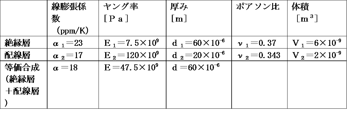
- Example 1 The core substrate 10 was made of aluminosilicate glass, and the thickness of the core substrate 10 was 300 ⁇ m. A wiring layer 30 having a thickness of 5 ⁇ m was formed by copper plating on both surfaces in the thickness direction of the core substrate 10 using a semi-additive method. After the wiring layer 30 was laminated on the core substrate 10, the insulating material 20, which is an epoxy compound resin, was laminated from both sides of the core substrate 10 by vacuum laminating at 190 ° C. to form the insulating layer 20. Furthermore, by repeating the formation of the wiring layer 30 and the formation of the insulating layer 20, the four wiring layers 30 and the three insulating layers 20 are laminated on both surfaces of the core substrate 10, thereby forming the wiring substrate 100 shown in FIG. 3. Got. The thickness d 1 of the insulating layer 20 was 60 ⁇ m on both surfaces of the core substrate 10.
- the package substrate 200 was obtained by dicing the core substrate 10 and separating the wiring substrate 100 into individual pieces.
- the width w 3 of the thin layer portion 21 was 120 ⁇ m, and the thickness d s of the thin layer portion 21 was 15 ⁇ m.
- Example 1 the values in Table 2 below were used for the linear expansion coefficient, Young's modulus, thickness, Poisson's ratio, and volume.
- TCT temperature cycle test
- Example 2 In the second embodiment, the width w 1 of the tip of the first dicing blade 50 is changed to 450 ⁇ m with respect to the wiring substrate 100 having the same conditions as the wiring substrate used in the first embodiment, and the tip of the second dicing blade 60 is changed.
- the other conditions including the width and other conditions were the same as in Example 1.
- the width w 1 of the both surfaces of the separation grooves 40 is 450 [mu] m
- a width w 3 of the thin layer portion 21 to obtain a packaging substrate 200 of 150 [mu] m.
- the temperature cycle test MIL-STD-883H giving a temperature change from 125 ° C. to ⁇ 55 ° C. was performed 1000 cycles on the ten package substrates 200 manufactured in Example 2. As a result, the reliability of the manufactured package substrate 200 such as cracking of the core substrate 10 did not decrease.
- Example 3 In the third embodiment, the width w 1 of the tip of the first dicing blade 50 is changed to 750 ⁇ m with respect to the wiring substrate 100 having the same conditions as the wiring substrate used in the first embodiment, and the tip of the second dicing blade 60 is changed.
- the other conditions including the width and other conditions were the same as in Example 1.
- the package substrate 200 in which the width w 1 of the separation groove 40 was 750 ⁇ m and the width w 3 of the thin layer portion 21 was 300 ⁇ m was obtained.
- the temperature cycle test MIL-STD-883H that gives a temperature change from 125 ° C. to ⁇ 55 ° C. was performed 1000 cycles on the ten package substrates 200 manufactured in Example 3. As a result, the reliability of the manufactured package substrate 200 such as cracking of the core substrate 10 did not decrease.
- Example 4 In Example 4, a package substrate 200 was obtained in the same manner as in Example 1 except that d s was set to 30 ⁇ m.
- the temperature cycle test MIL-STD-883H giving a temperature change from 125 ° C. to ⁇ 55 ° C. was performed 1000 cycles on the ten package substrates 200 manufactured in Example 4. As a result, the reliability of the manufactured package substrate 200 such as cracking of the core substrate 10 did not decrease.
- Example 5 a package substrate 200 was obtained in the same manner as in Example 1 except that ds was 45 ⁇ m.
- the temperature cycle test MIL-STD-883H which gives a temperature change from 125 ° C. to ⁇ 55 ° C., was performed 1000 cycles on the ten package substrates 200 manufactured in Example 5. As a result, the reliability of the manufactured package substrate 200 such as cracking of the core substrate 10 did not decrease.
- Comparative Example 1 A 10 mm ⁇ 10 mm package substrate was obtained in the same manner as in Example 1 except that the separation groove 40 was not formed, that is, the thin layer portion 21 was not formed. When the packaging substrate produced in Comparative Example 1 was left at room temperature for 3 days, 7 core substrates out of 10 were cracked.
- Comparative Example 2 In Comparative Example 2, 60 [mu] m width w 3 of the thin layer portion 21, 55 .mu.m and d m, except for using 5 ⁇ m to d s, in the same manner as in Example 1 to obtain a packaging substrate of 10 mm ⁇ 10 mm.
- the width w 3 of the thin layer portion 21 is set to 120 ⁇ m or more, whereby the core substrate It is considered that a package substrate capable of suppressing the occurrence of breakage on the cut surface can be provided.
- the width w 3 of the thin layer portion 21 is estimated by using the above (Equation 5) even if the condition of the laminated body of the insulating layer 20 and the wiring layer 30 changes. It is considered possible.
- the package substrate 200 of the present invention in which the thin layer portion 21 is formed by partially removing the outer peripheral portion of the insulating layer 20 is a minute one that leads to cracking of the core substrate 10. It is thought that the expansion of cracks due to thermal stress could be suppressed.
- the package substrate 200 is shown to be square when viewed from the upper surface side, but is not limited thereto, and is configured to be rectangular when viewed from the upper surface side. Also good.
Landscapes
- Engineering & Computer Science (AREA)
- Manufacturing & Machinery (AREA)
- Microelectronics & Electronic Packaging (AREA)
- Ceramic Engineering (AREA)
- Production Of Multi-Layered Print Wiring Board (AREA)
- Structure Of Printed Boards (AREA)
- Physics & Mathematics (AREA)
- Geometry (AREA)
- Chemical & Material Sciences (AREA)
- Dicing (AREA)
Abstract
Description
前記配線層及び前記絶縁層の線膨張係数をα[ppm/K]、前記配線層及び前記絶縁層のヤング率をE[Pa]、所定の温度差を△T[K]、前記配線層及び前記絶縁層の合成厚みをd[m]、および前記薄層部分の端部から反対側の薄層部分の端部までの長さをL[m]とすると、
前記w3は、以下の式:

図1は、本発明に係るパッケージ用基板の断面図である。図1に示されるように、パッケージ用基板200は、コア基板10と、絶縁層20と、コア基板10の厚さ方向の両面に積層された1又は複数の配線層30と、を含む。パッケージ用基板200は、絶縁層20において絶縁層20の厚さが部分的に薄くなるように構成された薄層部分21を有する。
コア基板10は、配線基板100およびパッケージ用基板200の電気特性を向上させる材料で構成することができる。例えば、コア基板10としては、ガラス基板、シリコン基板、セラミック基板、プラスチック板、プラスチックテープ等の脆性材料を用いることができる。コア基板10は、例えば、ソーダライムガラスやアルミノ珪酸塩ガラスなどで構成されたガラス基板とすることが好ましい。本発明のコア基板10に用いるガラス基板は、表面を当分野で一般的に行われている方法により処理されたものであってもよく、例えば、表面に粗化処理を行ったもの、フッ酸で処理したもの、または、ガラス基板表面にシリコン処理を施したものであってもよい。本発明の一態様において、コア基板10に用いるガラス基板は表面に下地層(図示せず)を形成してもよい。コア基板10の厚さは、特に限定されないが、好ましくは50μm~700μmである。
配線層30は、コア基板10の厚さ方向の表面上並びに/または絶縁層20の表面上及び/若しくは内部に形成される。本発明の一態様において、少なくとも一部の配線層30はコア基板10に接するように形成される。また、本発明の他の態様において、配線層30はコア基板と接しなくてもよい。配線層30は一層であってもよく、また複数の層であってもよい。
本発明の一態様において、絶縁層20は配線層30を埋め込むようにコア基板10及び配線層30上に形成される。絶縁層20は一層であってもよく、また複数の層であってもよい。
本発明の一態様のパッケージ用基板200は、これらに限定されるものではないが、図3~図9に示す工程にしたがって形成することができる。まず、図3に示すように、コア基板10の厚さ方向の表面に、上述した方法を用いて配線層30と絶縁層20を形成して、配線基板100を形成する。


d=d1 (式2)


以下、本発明の実施例について説明するが、以下の実施例は本発明の適用範囲を限定するものではない。
コア基板10をアルミノ珪酸塩ガラスで構成し、コア基板10の板厚寸法を300μmとした。セミアディティブ法を使用してコア基板10の厚さ方向の両面に銅めっきにより5μmの厚みの配線層30を形成した。コア基板10に配線層30を積層した後は、コア基板10の両面からエポキシ配合樹脂である絶縁性材料を190℃で真空ラミネートすることにより積層し、絶縁層20を形成した。さらに、配線層30の形成と絶縁層20の形成を繰り返すことで、コア基板10の両面に、4層の配線層30と3層の絶縁層20を積層することにより図3に示す配線基板100を得た。コア基板10の両面ともに、絶縁層20の厚みd1は60μmであった。
実施例2では、実施例1で用いた配線基板と同じ条件の配線基板100に対して、第1のダイシングブレード50の先端の幅w1を450μmに変更し、第2のダイシングブレード60の先端の幅等の条件を含めその他の条件は実施例1と同じにした。その結果、実施例2では、両面の分離溝40の幅w1が450μm、薄層部分21の幅w3が150μmのパッケージ用基板200を得た。
実施例3では、実施例1で用いた配線基板と同じ条件の配線基板100に対して、第1のダイシングブレード50の先端の幅w1を750μmに変更し、第2のダイシングブレード60の先端の幅等の条件を含めその他の条件は実施例1と同じにした。その結果、実施例3では、分離溝40の幅w1が750μm、薄層部分21の幅w3が300μmのパッケージ用基板200を得た。
実施例4では、dsを30μmとした以外は、実施例1と同様にすることにより、パッケージ用基板200を得た。
実施例5では、dsを45μmとした以外は、実施例1と同様にすることにより、パッケージ用基板200を得た。
(比較例1)
分離溝40を形成しない、すなわち薄層部分21を形成しない以外は、実施例1と同様にして、10mm×10mmのパッケージ用基板を得た。比較例1において作製したパッケージ用基板を3日常温で放置したところ、10個の内7個コア基板の割れが起きた。
比較例2では、薄層部分21の幅w3を60μm、dmを55μm、dsを5μmとした以外は、実施例1と同様にして、10mm×10mmのパッケージ用基板を得た。
以下の表3は各実施例及び比較例の評価結果をまとめたものである。


20 絶縁層
21 薄層部分
30 配線層
40 分離溝
50 第1のダイシングブレード
60 第2のダイシングブレード
100 配線基板
200 パッケージ用基板
Claims (6)
- コア基板と、
前記コア基板の片面又は両面上に形成された絶縁層と、
前記絶縁層上及び/又は前記絶縁層に埋め込まれるように形成された1又は複数の配線層と、
を含むパッケージ用基板であって、
前記パッケージ用基板は、前記絶縁層の外周部分に、前記絶縁層が部分的に薄くなった薄層部分を有する、パッケージ用基板。 - 前記コア基板はガラスで構成されている、請求項1に記載のパッケージ用基板。
- 前記薄層部分は、前記薄層部分の端部から前記絶縁層の段差面までの間の幅w3[m]を有し、
前記配線層及び前記絶縁層の線膨張係数をα[ppm/K]、前記配線層及び前記絶縁層のヤング率をE[Pa]、所定の温度差を△T[K]、前記配線層及び前記絶縁層の合成厚みをd[m]、および前記薄層部分の端部から反対側の薄層部分の端部までの長さをL[m]とすると、
前記w3は、以下の式:

- 前記w3は、120μm以上である、請求項2に記載のパッケージ用基板。
- パッケージ用基板の製造方法であって、
コア基板の片面又は両面に配線層及び絶縁層を形成して、配線基板を形成する工程と、
前記絶縁層の所定の位置に、第1のダイシングブレードを用いてダイシングすることにより、前記絶縁層が部分的に薄くなるように分離溝を形成する工程と、
前記分離溝の底面の溝幅の中央部分において、前記第1のダイシングブレードよりも先端の幅が狭い第2のダイシングブレードを用いてダイシングして前記絶縁層及び前記コア基板を切断することにより、前記絶縁層が部分的に薄くなった薄層部分を有する複数のパッケージ用基板を得る工程と、
を含む、パッケージ用基板の製造方法。 - 前記コア基板はガラスで構成されている、請求項5に記載のパッケージ用基板の製造方法。
Priority Applications (3)
| Application Number | Priority Date | Filing Date | Title |
|---|---|---|---|
| JP2017562887A JP6891815B2 (ja) | 2016-01-22 | 2017-01-19 | パッケージ用基板、およびその製造方法 |
| EP17741483.6A EP3407379B1 (en) | 2016-01-22 | 2017-01-19 | Package substrate and method for fabricating the same |
| US16/007,490 US10204854B2 (en) | 2016-01-22 | 2018-06-13 | Packaging substrate and method of fabricating the same |
Applications Claiming Priority (2)
| Application Number | Priority Date | Filing Date | Title |
|---|---|---|---|
| JP2016-010931 | 2016-01-22 | ||
| JP2016010931 | 2016-01-22 |
Related Child Applications (1)
| Application Number | Title | Priority Date | Filing Date |
|---|---|---|---|
| US16/007,490 Continuation US10204854B2 (en) | 2016-01-22 | 2018-06-13 | Packaging substrate and method of fabricating the same |
Publications (1)
| Publication Number | Publication Date |
|---|---|
| WO2017126606A1 true WO2017126606A1 (ja) | 2017-07-27 |
Family
ID=59362244
Family Applications (1)
| Application Number | Title | Priority Date | Filing Date |
|---|---|---|---|
| PCT/JP2017/001744 Ceased WO2017126606A1 (ja) | 2016-01-22 | 2017-01-19 | パッケージ用基板、およびその製造方法 |
Country Status (5)
| Country | Link |
|---|---|
| US (1) | US10204854B2 (ja) |
| EP (1) | EP3407379B1 (ja) |
| JP (1) | JP6891815B2 (ja) |
| TW (1) | TWI738706B (ja) |
| WO (1) | WO2017126606A1 (ja) |
Cited By (4)
| Publication number | Priority date | Publication date | Assignee | Title |
|---|---|---|---|---|
| JP2019102779A (ja) * | 2017-11-28 | 2019-06-24 | サムソン エレクトロ−メカニックス カンパニーリミテッド. | キャリア基板及び上記キャリア基板を用いた半導体パッケージの製造方法 |
| JP2021509542A (ja) * | 2018-02-28 | 2021-03-25 | ロジャーズ ジャーマニー ゲーエムベーハーRogers Germany GmbH | 金属セラミック基板および金属セラミック基板の製造方法 |
| DE102024125859A1 (de) * | 2024-09-09 | 2026-03-12 | Gebr. Schmid Gmbh | Verfahren zur Herstellung mehrschichtiger Substrate mit einer integrierten Leiterstruktur und gemäss dem Verfahren herstellbare mehrschichtige Substrate |
| WO2026070757A1 (ja) * | 2024-09-30 | 2026-04-02 | 株式会社ミクロ技術研究所 | ガラス配線基板の製造方法 |
Families Citing this family (4)
| Publication number | Priority date | Publication date | Assignee | Title |
|---|---|---|---|---|
| KR101605172B1 (ko) * | 2015-04-07 | 2016-03-22 | 삼성전자주식회사 | 패키지 기판 및 그 제조방법 |
| WO2020149374A1 (ja) * | 2019-01-16 | 2020-07-23 | 凸版印刷株式会社 | パッケージ用基板、およびその製造方法 |
| CN115172176B (zh) * | 2022-09-06 | 2023-09-22 | 合肥圣达电子科技实业有限公司 | 陶瓷基板及其制备方法、微波器件及其封装外壳结构 |
| CN116884964B (zh) * | 2023-08-04 | 2024-03-26 | 江苏诚盛科技有限公司 | 一种led芯片封装方法 |
Citations (5)
| Publication number | Priority date | Publication date | Assignee | Title |
|---|---|---|---|---|
| JP2007019394A (ja) * | 2005-07-11 | 2007-01-25 | Toshiba Corp | 半導体パッケージの製造方法及びこの製造方法により形成された半導体パッケージ |
| JP2010016291A (ja) * | 2008-07-07 | 2010-01-21 | Shinko Electric Ind Co Ltd | 配線基板及び半導体装置の製造方法 |
| JP2015079795A (ja) * | 2013-10-15 | 2015-04-23 | 新光電気工業株式会社 | 配線基板、半導体装置及び配線基板の製造方法 |
| US20150334823A1 (en) * | 2014-05-19 | 2015-11-19 | Dyi-chung Hu | Substrate components for packaging ic chips and electronic device packages of the same |
| JP2015231005A (ja) | 2014-06-06 | 2015-12-21 | 日本特殊陶業株式会社 | 配線基板およびその製造方法 |
Family Cites Families (5)
| Publication number | Priority date | Publication date | Assignee | Title |
|---|---|---|---|---|
| JPS62142396A (ja) * | 1985-12-17 | 1987-06-25 | アルプス電気株式会社 | 薄膜回路基板 |
| TWI489519B (zh) * | 2004-04-28 | 2015-06-21 | 半導體能源研究所股份有限公司 | 基板上配線,半導體裝置及其製造方法 |
| JP4614278B2 (ja) * | 2005-05-25 | 2011-01-19 | アルプス電気株式会社 | 電子回路ユニット、及びその製造方法 |
| JP2008288285A (ja) * | 2007-05-15 | 2008-11-27 | Sharp Corp | 積層基板の切断方法、半導体装置の製造方法、半導体装置、発光装置及びバックライト装置 |
| US20140035935A1 (en) * | 2012-08-03 | 2014-02-06 | Qualcomm Mems Technologies, Inc. | Passives via bar |
-
2017
- 2017-01-19 EP EP17741483.6A patent/EP3407379B1/en active Active
- 2017-01-19 JP JP2017562887A patent/JP6891815B2/ja active Active
- 2017-01-19 TW TW106101782A patent/TWI738706B/zh active
- 2017-01-19 WO PCT/JP2017/001744 patent/WO2017126606A1/ja not_active Ceased
-
2018
- 2018-06-13 US US16/007,490 patent/US10204854B2/en active Active
Patent Citations (5)
| Publication number | Priority date | Publication date | Assignee | Title |
|---|---|---|---|---|
| JP2007019394A (ja) * | 2005-07-11 | 2007-01-25 | Toshiba Corp | 半導体パッケージの製造方法及びこの製造方法により形成された半導体パッケージ |
| JP2010016291A (ja) * | 2008-07-07 | 2010-01-21 | Shinko Electric Ind Co Ltd | 配線基板及び半導体装置の製造方法 |
| JP2015079795A (ja) * | 2013-10-15 | 2015-04-23 | 新光電気工業株式会社 | 配線基板、半導体装置及び配線基板の製造方法 |
| US20150334823A1 (en) * | 2014-05-19 | 2015-11-19 | Dyi-chung Hu | Substrate components for packaging ic chips and electronic device packages of the same |
| JP2015231005A (ja) | 2014-06-06 | 2015-12-21 | 日本特殊陶業株式会社 | 配線基板およびその製造方法 |
Non-Patent Citations (1)
| Title |
|---|
| See also references of EP3407379A4 |
Cited By (5)
| Publication number | Priority date | Publication date | Assignee | Title |
|---|---|---|---|---|
| JP2019102779A (ja) * | 2017-11-28 | 2019-06-24 | サムソン エレクトロ−メカニックス カンパニーリミテッド. | キャリア基板及び上記キャリア基板を用いた半導体パッケージの製造方法 |
| JP2021509542A (ja) * | 2018-02-28 | 2021-03-25 | ロジャーズ ジャーマニー ゲーエムベーハーRogers Germany GmbH | 金属セラミック基板および金属セラミック基板の製造方法 |
| JP7033660B2 (ja) | 2018-02-28 | 2022-03-10 | ロジャーズ ジャーマニー ゲーエムベーハー | 金属セラミック基板および金属セラミック基板の製造方法 |
| DE102024125859A1 (de) * | 2024-09-09 | 2026-03-12 | Gebr. Schmid Gmbh | Verfahren zur Herstellung mehrschichtiger Substrate mit einer integrierten Leiterstruktur und gemäss dem Verfahren herstellbare mehrschichtige Substrate |
| WO2026070757A1 (ja) * | 2024-09-30 | 2026-04-02 | 株式会社ミクロ技術研究所 | ガラス配線基板の製造方法 |
Also Published As
| Publication number | Publication date |
|---|---|
| TWI738706B (zh) | 2021-09-11 |
| JP6891815B2 (ja) | 2021-06-18 |
| JPWO2017126606A1 (ja) | 2018-11-08 |
| US20180294217A1 (en) | 2018-10-11 |
| EP3407379A4 (en) | 2019-10-09 |
| EP3407379A1 (en) | 2018-11-28 |
| US10204854B2 (en) | 2019-02-12 |
| EP3407379B1 (en) | 2024-08-14 |
| TW201737426A (zh) | 2017-10-16 |
Similar Documents
| Publication | Publication Date | Title |
|---|---|---|
| JP6891815B2 (ja) | パッケージ用基板、およびその製造方法 | |
| JP6427817B2 (ja) | 印刷回路基板及びその製造方法 | |
| JP2022078155A (ja) | パッケージ用基板 | |
| JP6805511B2 (ja) | 配線基板、およびその製造方法 | |
| EP2958142B1 (en) | High density film for ic package | |
| JP6863458B2 (ja) | 積層型電子部品 | |
| CN105578710B (zh) | 印刷电路板及其制造方法 | |
| WO2020149374A1 (ja) | パッケージ用基板、およびその製造方法 | |
| JP2017147395A (ja) | パッケージ用基板、およびその製造方法 | |
| JP2017220647A (ja) | パッケージ用基板 | |
| JP5468445B2 (ja) | 半導体装置及びその製造方法 | |
| JP6724775B2 (ja) | 配線基板の個片化方法及びパッケージ用基板 | |
| JP2015231005A (ja) | 配線基板およびその製造方法 | |
| CN112586092B (zh) | 布线基板以及电子装置 | |
| CN109427729B (zh) | 半导体装置封装和其制造方法 | |
| JP2019009151A (ja) | パッケージ用基板、およびその製造方法 | |
| JP2016143725A (ja) | プリント配線板およびその製造方法 | |
| TWI576020B (zh) | Printed wiring board and manufacturing method thereof | |
| JP6904044B2 (ja) | 半導体パッケージ用基板およびその製造方法 | |
| JP2017118053A (ja) | パッケージ基板及びその製造方法 | |
| KR102281457B1 (ko) | 인쇄회로기판 및 이의 제조방법 | |
| JP7181839B2 (ja) | 配線基板、および配線基板の製造方法 | |
| JP3836572B2 (ja) | 薄膜電子部品の製造方法 | |
| US20150156891A1 (en) | Printed circuit board and manufacturing method thereof | |
| JP2019004077A (ja) | 配線基板 |
Legal Events
| Date | Code | Title | Description |
|---|---|---|---|
| 121 | Ep: the epo has been informed by wipo that ep was designated in this application |
Ref document number: 17741483 Country of ref document: EP Kind code of ref document: A1 |
|
| ENP | Entry into the national phase |
Ref document number: 2017562887 Country of ref document: JP Kind code of ref document: A |
|
| NENP | Non-entry into the national phase |
Ref country code: DE |
|
| WWE | Wipo information: entry into national phase |
Ref document number: 2017741483 Country of ref document: EP |
|
| ENP | Entry into the national phase |
Ref document number: 2017741483 Country of ref document: EP Effective date: 20180822 |