WO2017128794A1 - 减反射结构及其制造方法、显示器及其制造方法 - Google Patents
减反射结构及其制造方法、显示器及其制造方法 Download PDFInfo
- Publication number
- WO2017128794A1 WO2017128794A1 PCT/CN2016/104176 CN2016104176W WO2017128794A1 WO 2017128794 A1 WO2017128794 A1 WO 2017128794A1 CN 2016104176 W CN2016104176 W CN 2016104176W WO 2017128794 A1 WO2017128794 A1 WO 2017128794A1
- Authority
- WO
- WIPO (PCT)
- Prior art keywords
- reflection structure
- alignment layer
- retardation film
- layer
- substrate
- Prior art date
- Legal status (The legal status is an assumption and is not a legal conclusion. Google has not performed a legal analysis and makes no representation as to the accuracy of the status listed.)
- Ceased
Links
Images




Classifications
-
- G—PHYSICS
- G02—OPTICS
- G02B—OPTICAL ELEMENTS, SYSTEMS OR APPARATUS
- G02B1/00—Optical elements characterised by the material of which they are made; Optical coatings for optical elements
- G02B1/10—Optical coatings produced by application to, or surface treatment of, optical elements
- G02B1/11—Anti-reflection coatings
-
- G—PHYSICS
- G02—OPTICS
- G02B—OPTICAL ELEMENTS, SYSTEMS OR APPARATUS
- G02B1/00—Optical elements characterised by the material of which they are made; Optical coatings for optical elements
- G02B1/10—Optical coatings produced by application to, or surface treatment of, optical elements
- G02B1/11—Anti-reflection coatings
- G02B1/111—Anti-reflection coatings using layers comprising organic materials
-
- G—PHYSICS
- G02—OPTICS
- G02B—OPTICAL ELEMENTS, SYSTEMS OR APPARATUS
- G02B1/00—Optical elements characterised by the material of which they are made; Optical coatings for optical elements
- G02B1/10—Optical coatings produced by application to, or surface treatment of, optical elements
- G02B1/11—Anti-reflection coatings
- G02B1/113—Anti-reflection coatings using inorganic layer materials only
-
- G—PHYSICS
- G02—OPTICS
- G02B—OPTICAL ELEMENTS, SYSTEMS OR APPARATUS
- G02B5/00—Optical elements other than lenses
- G02B5/30—Polarising elements
- G02B5/3025—Polarisers, i.e. arrangements capable of producing a definite output polarisation state from an unpolarised input state
- G02B5/3033—Polarisers, i.e. arrangements capable of producing a definite output polarisation state from an unpolarised input state in the form of a thin sheet or foil, e.g. Polaroid
-
- G—PHYSICS
- G02—OPTICS
- G02B—OPTICAL ELEMENTS, SYSTEMS OR APPARATUS
- G02B5/00—Optical elements other than lenses
- G02B5/30—Polarising elements
- G02B5/3025—Polarisers, i.e. arrangements capable of producing a definite output polarisation state from an unpolarised input state
- G02B5/3033—Polarisers, i.e. arrangements capable of producing a definite output polarisation state from an unpolarised input state in the form of a thin sheet or foil, e.g. Polaroid
- G02B5/3041—Polarisers, i.e. arrangements capable of producing a definite output polarisation state from an unpolarised input state in the form of a thin sheet or foil, e.g. Polaroid comprising multiple thin layers, e.g. multilayer stacks
- G02B5/305—Polarisers, i.e. arrangements capable of producing a definite output polarisation state from an unpolarised input state in the form of a thin sheet or foil, e.g. Polaroid comprising multiple thin layers, e.g. multilayer stacks including organic materials, e.g. polymeric layers
-
- G—PHYSICS
- G02—OPTICS
- G02B—OPTICAL ELEMENTS, SYSTEMS OR APPARATUS
- G02B5/00—Optical elements other than lenses
- G02B5/30—Polarising elements
- G02B5/3083—Birefringent or phase retarding elements
-
- G—PHYSICS
- G02—OPTICS
- G02F—OPTICAL DEVICES OR ARRANGEMENTS FOR THE CONTROL OF LIGHT BY MODIFICATION OF THE OPTICAL PROPERTIES OF THE MEDIA OF THE ELEMENTS INVOLVED THEREIN; NON-LINEAR OPTICS; FREQUENCY-CHANGING OF LIGHT; OPTICAL LOGIC ELEMENTS; OPTICAL ANALOGUE/DIGITAL CONVERTERS
- G02F1/00—Devices or arrangements for the control of the intensity, colour, phase, polarisation or direction of light arriving from an independent light source, e.g. switching, gating or modulating; Non-linear optics
- G02F1/01—Devices or arrangements for the control of the intensity, colour, phase, polarisation or direction of light arriving from an independent light source, e.g. switching, gating or modulating; Non-linear optics for the control of the intensity, phase, polarisation or colour
- G02F1/13—Devices or arrangements for the control of the intensity, colour, phase, polarisation or direction of light arriving from an independent light source, e.g. switching, gating or modulating; Non-linear optics for the control of the intensity, phase, polarisation or colour based on liquid crystals, e.g. single liquid crystal display cells
- G02F1/133—Constructional arrangements; Operation of liquid crystal cells; Circuit arrangements
- G02F1/1333—Constructional arrangements; Manufacturing methods
- G02F1/133305—Flexible substrates, e.g. plastics, organic film
-
- G—PHYSICS
- G02—OPTICS
- G02F—OPTICAL DEVICES OR ARRANGEMENTS FOR THE CONTROL OF LIGHT BY MODIFICATION OF THE OPTICAL PROPERTIES OF THE MEDIA OF THE ELEMENTS INVOLVED THEREIN; NON-LINEAR OPTICS; FREQUENCY-CHANGING OF LIGHT; OPTICAL LOGIC ELEMENTS; OPTICAL ANALOGUE/DIGITAL CONVERTERS
- G02F1/00—Devices or arrangements for the control of the intensity, colour, phase, polarisation or direction of light arriving from an independent light source, e.g. switching, gating or modulating; Non-linear optics
- G02F1/01—Devices or arrangements for the control of the intensity, colour, phase, polarisation or direction of light arriving from an independent light source, e.g. switching, gating or modulating; Non-linear optics for the control of the intensity, phase, polarisation or colour
- G02F1/13—Devices or arrangements for the control of the intensity, colour, phase, polarisation or direction of light arriving from an independent light source, e.g. switching, gating or modulating; Non-linear optics for the control of the intensity, phase, polarisation or colour based on liquid crystals, e.g. single liquid crystal display cells
- G02F1/133—Constructional arrangements; Operation of liquid crystal cells; Circuit arrangements
- G02F1/1333—Constructional arrangements; Manufacturing methods
- G02F1/1335—Structural association of cells with optical devices, e.g. polarisers or reflectors
- G02F1/133502—Antiglare, refractive index matching layers
-
- G—PHYSICS
- G02—OPTICS
- G02F—OPTICAL DEVICES OR ARRANGEMENTS FOR THE CONTROL OF LIGHT BY MODIFICATION OF THE OPTICAL PROPERTIES OF THE MEDIA OF THE ELEMENTS INVOLVED THEREIN; NON-LINEAR OPTICS; FREQUENCY-CHANGING OF LIGHT; OPTICAL LOGIC ELEMENTS; OPTICAL ANALOGUE/DIGITAL CONVERTERS
- G02F1/00—Devices or arrangements for the control of the intensity, colour, phase, polarisation or direction of light arriving from an independent light source, e.g. switching, gating or modulating; Non-linear optics
- G02F1/01—Devices or arrangements for the control of the intensity, colour, phase, polarisation or direction of light arriving from an independent light source, e.g. switching, gating or modulating; Non-linear optics for the control of the intensity, phase, polarisation or colour
- G02F1/13—Devices or arrangements for the control of the intensity, colour, phase, polarisation or direction of light arriving from an independent light source, e.g. switching, gating or modulating; Non-linear optics for the control of the intensity, phase, polarisation or colour based on liquid crystals, e.g. single liquid crystal display cells
- G02F1/133—Constructional arrangements; Operation of liquid crystal cells; Circuit arrangements
- G02F1/1333—Constructional arrangements; Manufacturing methods
- G02F1/1335—Structural association of cells with optical devices, e.g. polarisers or reflectors
- G02F1/133528—Polarisers
-
- G—PHYSICS
- G02—OPTICS
- G02F—OPTICAL DEVICES OR ARRANGEMENTS FOR THE CONTROL OF LIGHT BY MODIFICATION OF THE OPTICAL PROPERTIES OF THE MEDIA OF THE ELEMENTS INVOLVED THEREIN; NON-LINEAR OPTICS; FREQUENCY-CHANGING OF LIGHT; OPTICAL LOGIC ELEMENTS; OPTICAL ANALOGUE/DIGITAL CONVERTERS
- G02F1/00—Devices or arrangements for the control of the intensity, colour, phase, polarisation or direction of light arriving from an independent light source, e.g. switching, gating or modulating; Non-linear optics
- G02F1/01—Devices or arrangements for the control of the intensity, colour, phase, polarisation or direction of light arriving from an independent light source, e.g. switching, gating or modulating; Non-linear optics for the control of the intensity, phase, polarisation or colour
- G02F1/13—Devices or arrangements for the control of the intensity, colour, phase, polarisation or direction of light arriving from an independent light source, e.g. switching, gating or modulating; Non-linear optics for the control of the intensity, phase, polarisation or colour based on liquid crystals, e.g. single liquid crystal display cells
- G02F1/133—Constructional arrangements; Operation of liquid crystal cells; Circuit arrangements
- G02F1/1333—Constructional arrangements; Manufacturing methods
- G02F1/1335—Structural association of cells with optical devices, e.g. polarisers or reflectors
- G02F1/13363—Birefringent elements, e.g. for optical compensation
-
- H—ELECTRICITY
- H10—SEMICONDUCTOR DEVICES; ELECTRIC SOLID-STATE DEVICES NOT OTHERWISE PROVIDED FOR
- H10K—ORGANIC ELECTRIC SOLID-STATE DEVICES
- H10K59/00—Integrated devices, or assemblies of multiple devices, comprising at least one organic light-emitting element covered by group H10K50/00
- H10K59/10—OLED displays
- H10K59/12—Active-matrix OLED [AMOLED] displays
-
- H—ELECTRICITY
- H10—SEMICONDUCTOR DEVICES; ELECTRIC SOLID-STATE DEVICES NOT OTHERWISE PROVIDED FOR
- H10K—ORGANIC ELECTRIC SOLID-STATE DEVICES
- H10K59/00—Integrated devices, or assemblies of multiple devices, comprising at least one organic light-emitting element covered by group H10K50/00
- H10K59/10—OLED displays
- H10K59/12—Active-matrix OLED [AMOLED] displays
- H10K59/1201—Manufacture or treatment
-
- G—PHYSICS
- G02—OPTICS
- G02F—OPTICAL DEVICES OR ARRANGEMENTS FOR THE CONTROL OF LIGHT BY MODIFICATION OF THE OPTICAL PROPERTIES OF THE MEDIA OF THE ELEMENTS INVOLVED THEREIN; NON-LINEAR OPTICS; FREQUENCY-CHANGING OF LIGHT; OPTICAL LOGIC ELEMENTS; OPTICAL ANALOGUE/DIGITAL CONVERTERS
- G02F1/00—Devices or arrangements for the control of the intensity, colour, phase, polarisation or direction of light arriving from an independent light source, e.g. switching, gating or modulating; Non-linear optics
- G02F1/01—Devices or arrangements for the control of the intensity, colour, phase, polarisation or direction of light arriving from an independent light source, e.g. switching, gating or modulating; Non-linear optics for the control of the intensity, phase, polarisation or colour
- G02F1/13—Devices or arrangements for the control of the intensity, colour, phase, polarisation or direction of light arriving from an independent light source, e.g. switching, gating or modulating; Non-linear optics for the control of the intensity, phase, polarisation or colour based on liquid crystals, e.g. single liquid crystal display cells
- G02F1/133—Constructional arrangements; Operation of liquid crystal cells; Circuit arrangements
- G02F1/1333—Constructional arrangements; Manufacturing methods
- G02F1/1335—Structural association of cells with optical devices, e.g. polarisers or reflectors
- G02F1/133528—Polarisers
- G02F1/133531—Polarisers characterised by the arrangement of polariser or analyser axes
-
- G—PHYSICS
- G02—OPTICS
- G02F—OPTICAL DEVICES OR ARRANGEMENTS FOR THE CONTROL OF LIGHT BY MODIFICATION OF THE OPTICAL PROPERTIES OF THE MEDIA OF THE ELEMENTS INVOLVED THEREIN; NON-LINEAR OPTICS; FREQUENCY-CHANGING OF LIGHT; OPTICAL LOGIC ELEMENTS; OPTICAL ANALOGUE/DIGITAL CONVERTERS
- G02F1/00—Devices or arrangements for the control of the intensity, colour, phase, polarisation or direction of light arriving from an independent light source, e.g. switching, gating or modulating; Non-linear optics
- G02F1/01—Devices or arrangements for the control of the intensity, colour, phase, polarisation or direction of light arriving from an independent light source, e.g. switching, gating or modulating; Non-linear optics for the control of the intensity, phase, polarisation or colour
- G02F1/13—Devices or arrangements for the control of the intensity, colour, phase, polarisation or direction of light arriving from an independent light source, e.g. switching, gating or modulating; Non-linear optics for the control of the intensity, phase, polarisation or colour based on liquid crystals, e.g. single liquid crystal display cells
- G02F1/133—Constructional arrangements; Operation of liquid crystal cells; Circuit arrangements
- G02F1/1333—Constructional arrangements; Manufacturing methods
- G02F1/1335—Structural association of cells with optical devices, e.g. polarisers or reflectors
- G02F1/13356—Structural association of cells with optical devices, e.g. polarisers or reflectors characterised by the placement of the optical elements
- G02F1/133562—Structural association of cells with optical devices, e.g. polarisers or reflectors characterised by the placement of the optical elements on the viewer side
-
- G—PHYSICS
- G02—OPTICS
- G02F—OPTICAL DEVICES OR ARRANGEMENTS FOR THE CONTROL OF LIGHT BY MODIFICATION OF THE OPTICAL PROPERTIES OF THE MEDIA OF THE ELEMENTS INVOLVED THEREIN; NON-LINEAR OPTICS; FREQUENCY-CHANGING OF LIGHT; OPTICAL LOGIC ELEMENTS; OPTICAL ANALOGUE/DIGITAL CONVERTERS
- G02F1/00—Devices or arrangements for the control of the intensity, colour, phase, polarisation or direction of light arriving from an independent light source, e.g. switching, gating or modulating; Non-linear optics
- G02F1/01—Devices or arrangements for the control of the intensity, colour, phase, polarisation or direction of light arriving from an independent light source, e.g. switching, gating or modulating; Non-linear optics for the control of the intensity, phase, polarisation or colour
- G02F1/13—Devices or arrangements for the control of the intensity, colour, phase, polarisation or direction of light arriving from an independent light source, e.g. switching, gating or modulating; Non-linear optics for the control of the intensity, phase, polarisation or colour based on liquid crystals, e.g. single liquid crystal display cells
- G02F1/133—Constructional arrangements; Operation of liquid crystal cells; Circuit arrangements
- G02F1/1333—Constructional arrangements; Manufacturing methods
- G02F1/1335—Structural association of cells with optical devices, e.g. polarisers or reflectors
- G02F1/13363—Birefringent elements, e.g. for optical compensation
- G02F1/133635—Multifunctional compensators
-
- G—PHYSICS
- G02—OPTICS
- G02F—OPTICAL DEVICES OR ARRANGEMENTS FOR THE CONTROL OF LIGHT BY MODIFICATION OF THE OPTICAL PROPERTIES OF THE MEDIA OF THE ELEMENTS INVOLVED THEREIN; NON-LINEAR OPTICS; FREQUENCY-CHANGING OF LIGHT; OPTICAL LOGIC ELEMENTS; OPTICAL ANALOGUE/DIGITAL CONVERTERS
- G02F1/00—Devices or arrangements for the control of the intensity, colour, phase, polarisation or direction of light arriving from an independent light source, e.g. switching, gating or modulating; Non-linear optics
- G02F1/01—Devices or arrangements for the control of the intensity, colour, phase, polarisation or direction of light arriving from an independent light source, e.g. switching, gating or modulating; Non-linear optics for the control of the intensity, phase, polarisation or colour
- G02F1/13—Devices or arrangements for the control of the intensity, colour, phase, polarisation or direction of light arriving from an independent light source, e.g. switching, gating or modulating; Non-linear optics for the control of the intensity, phase, polarisation or colour based on liquid crystals, e.g. single liquid crystal display cells
- G02F1/133—Constructional arrangements; Operation of liquid crystal cells; Circuit arrangements
- G02F1/1333—Constructional arrangements; Manufacturing methods
- G02F1/1335—Structural association of cells with optical devices, e.g. polarisers or reflectors
- G02F1/13363—Birefringent elements, e.g. for optical compensation
- G02F1/133638—Waveplates, i.e. plates with a retardation value of lambda/n
-
- G—PHYSICS
- G02—OPTICS
- G02F—OPTICAL DEVICES OR ARRANGEMENTS FOR THE CONTROL OF LIGHT BY MODIFICATION OF THE OPTICAL PROPERTIES OF THE MEDIA OF THE ELEMENTS INVOLVED THEREIN; NON-LINEAR OPTICS; FREQUENCY-CHANGING OF LIGHT; OPTICAL LOGIC ELEMENTS; OPTICAL ANALOGUE/DIGITAL CONVERTERS
- G02F1/00—Devices or arrangements for the control of the intensity, colour, phase, polarisation or direction of light arriving from an independent light source, e.g. switching, gating or modulating; Non-linear optics
- G02F1/01—Devices or arrangements for the control of the intensity, colour, phase, polarisation or direction of light arriving from an independent light source, e.g. switching, gating or modulating; Non-linear optics for the control of the intensity, phase, polarisation or colour
- G02F1/13—Devices or arrangements for the control of the intensity, colour, phase, polarisation or direction of light arriving from an independent light source, e.g. switching, gating or modulating; Non-linear optics for the control of the intensity, phase, polarisation or colour based on liquid crystals, e.g. single liquid crystal display cells
- G02F1/133—Constructional arrangements; Operation of liquid crystal cells; Circuit arrangements
- G02F1/1333—Constructional arrangements; Manufacturing methods
- G02F1/1337—Surface-induced orientation of the liquid crystal molecules, e.g. by alignment layers
Definitions
- Embodiments of the present invention relate to an anti-reflection structure, a method of fabricating the same, a display, and a method of fabricating the same.
- the flexible display has become one of the main trends of display technology due to its thin thickness, light weight, bendability and even curlability, and has a promising future market.
- a polarizer attached to the outside of the display panel is generally used as an anti-reflection structure, but such an anti-reflection structure has a large thickness, for example, a commonly used polarizer
- the thickness of the retardation film is between 100 and 150 ⁇ m, and the thickness of the antireflection structure formed by the two is between 120 and 250 ⁇ m.
- the use of this structure makes the thickness of the flexible display large, which makes the flexible display thick, loses its thinness and is not suitable for flexible display.
- At least one embodiment of the present invention provides an anti-reflection structure, a method of fabricating the same, a display, and a method of fabricating the same, wherein the anti-reflection structure has a small thickness, and the display including the anti-reflection structure can not only realize a light and thin flexible display, but further It also guarantees a high degree of polarization.
- At least one embodiment of the present invention provides an anti-reflection structure comprising: a retardation film, a linear polarizing plate, and at least one alignment layer configured to orient the retardation film and the linear polarization film, wherein the retardation film and The linear polarizing plate includes a liquid crystal.
- At least one embodiment of the present invention further provides a display comprising: a display panel and the anti-reflection structure as described above, wherein the display panel comprises an array substrate and an opposite substrate disposed opposite to the array substrate, wherein The anti-reflection structure is disposed between the array substrate and the opposite substrate; or the anti-reflection structure is located at an opposite side of the array substrate from the array substrate side.
- At least one embodiment of the present invention further provides a method of manufacturing a display, comprising: providing a display panel, the display panel including an array substrate and a counter substrate opposite to each other, the array substrate comprising: a substrate; and a plurality of a pixel unit formed on the base substrate and having an organic light emitting diode and a thin film transistor formed in each of the plurality of pixel units, wherein the plurality of pixel units are located on the opposite substrate and the substrate Between the substrates; manufacturing the anti-reflection structure, comprising: forming a retardation film, a first alignment layer, and a linear polarization plate on the base substrate on which the organic light emitting diode and the thin film transistor are formed or on the opposite substrate; The first alignment layer is located between the retardation film and the linear polarizer, and the retardation film and the linear polarizer comprise liquid crystal.
- At least one embodiment of the present invention also provides a method of fabricating an anti-reflection structure, comprising: preparing a substrate; forming a retardation film, a first alignment layer, and a linear polarization plate on the substrate, wherein the first alignment layer is located at Between the retardation film and the linear polarizing plate, the retardation film and the linear polarizing plate comprise liquid crystal.
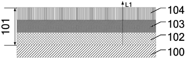
- FIG. 1a and 1b are respectively schematic diagrams showing two exemplary structures of an anti-reflection structure according to an embodiment of the present invention
- FIG. 2 is a schematic structural view of a display including an anti-reflection structure according to an embodiment of the present invention
- FIG. 3 is a schematic structural view of a display in which an anti-reflection structure is disposed in a display panel according to an embodiment of the present invention
- FIG. 4a is a schematic structural view of a display provided with an anti-reflection structure on a substrate according to an embodiment of the present invention
- 4b is a schematic structural view of a display provided with an anti-reflection structure on a counter substrate according to an embodiment of the invention
- 4c is another schematic structural view of a display in which an anti-reflection structure is disposed on a substrate according to an embodiment of the present invention
- 4d is a display of an anti-reflection structure disposed on a counter substrate according to an embodiment of the present invention Another structural diagram;
- 4e is a schematic structural view of a display of an anti-reflection structure disposed on a substrate according to an embodiment of the invention.
- Figure 5 is a cross-sectional structural view of a display according to an embodiment of the present invention.
- FIG. 6 is a schematic diagram showing the relationship between the degree of polarization of the anti-reflection structure and the wavelength of the incident light
- FIG. 7 is a graph showing transmittance of a light-cut layer according to an embodiment of the present invention.
- FIG. 8a to 8e are cross-sectional views showing a structure obtained after performing each step of manufacturing an anti-reflection structure in a manufacturing method according to an embodiment of the present invention.
- 9a to 9d are structural cross-sectional views obtained after performing the steps of manufacturing an anti-reflection structure on a counter substrate in a manufacturing method according to an embodiment of the present invention.
- FIG. 10 is a flow chart showing formation of an anti-reflection structure on a substrate in a manufacturing method according to an embodiment of the present invention
- FIG. 11 is a flow chart of forming an anti-reflection structure on a counter substrate in a manufacturing method according to an embodiment of the present invention, wherein an anti-reflection structure is disposed on a side of the opposite substrate opposite to the array substrate;
- FIG. 12 is a flow chart of forming an anti-reflection structure on a counter substrate in a manufacturing method according to an embodiment of the present invention, wherein an anti-reflection structure is disposed between the opposite substrate and the array substrate.
- At least one embodiment of the present invention provides an anti-reflection structure, a method of fabricating the same, a display, and a method of fabricating the same.
- the anti-reflection structure sequentially includes: a retardation film; a first alignment layer disposed on a light-emitting side of the retardation film; and a linear polarization plate disposed on a light-emitting side of the first alignment layer; wherein the retardation film and the The linear polarizing plate includes a liquid crystal.
- the anti-reflection structure according to an embodiment of the present invention has a significantly reduced thickness with respect to the existing anti-reflection structure attached to the outside of the flexible display panel, so that the display using the anti-reflection structure can realize ultra-thin display.
- the anti-reflection structure according to the embodiment of the present invention in order to obtain a higher degree of polarization while thinning the anti-reflection structure, the anti-reflection structure according to the embodiment of the present invention further provides a light-cut layer, which is configured to be cut off to be disadvantageous to polarized light. The increased light, thereby achieving a higher degree of polarization while reducing the thickness.
- the anti-reflection structure 101 sequentially includes a retardation film 102, a first alignment layer 103, and a linear polarization plate 104.
- the first alignment layer 103 is disposed on the light exit side of the retardation film 102;
- the linear polarizer 104 is disposed on the light exit side of the first alignment layer 103, wherein the retardation film and the linear polarizer include liquid crystal.
- the light-emitting side is relative to the display light, and the light-emitting side refers to the side located in the light-emitting direction of the display light, and the corresponding light-in side in the following description refers to the display light.
- L1 indicates the light outgoing direction of the display light.
- the retardation film and the liquid crystal included in the linear polarizing plate may be a polymerizable liquid crystal
- the linear polarizing plate 104 may include a dichroic dye, a polymerizable liquid crystal, and a photoinitiator
- the retardation film 102 may include a polymerizable liquid crystal and light.
- the dichroic dye may be X11 (BASF) or S-428
- the polymerizable liquid crystal may be a common nematic liquid crystal such as LC242 (merck)
- the photoinitiator may be 184.
- the linear polarizer 104 may include a dichroic dye having a mass percentage of 1% to 20%.
- the material, the mass percentage is 75%-95% of the polymerizable liquid crystal and the mass percentage is 0.1%-5% of the photoinitiator.
- the percentages of the dichroic dye, the polymerizable liquid crystal, and the photoinitiator are 10%, 87.5%, and 2.5%, respectively.
- the retardation film 102 may include from 75% to 99.5% by weight of the polymerizable liquid crystal and from 0.5% to 25% by weight of the photoinitiator.
- a retardation film including a liquid crystal material is required to be oriented during formation. 102 also needs to be oriented during the formation process.
- the linear polarizing plate 104 and the retardation film 102 may be aligned by sharing the first alignment layer 103 therebetween; or, the linear polarization plate 104 and the retardation film 102 may be aligned with different alignment layers, respectively.
- the first alignment layer 103 may be configured to orient the retardation film 102, and the anti-reflection structure may further include a second alignment layer 109 disposed on the light exit side of the in-line polarizer 104, and the The second alignment layer 109 is configured to orient the linear polarizing plate 104.
- the first alignment layer 103 may also be configured to orient the linearly polarizing plate 104, and the anti-reflection structure 101 may include a third alignment layer 130 disposed on the light incident side of the retardation film 102 and It is configured to orient the retardation film 102.
- both the linearly polarizing plate and the retardation film of the anti-reflection structure are formed using a liquid crystal material, for example, by a coating method, which is reduced according to an embodiment of the present invention as compared with a conventional anti-reflection structure for a display.
- the thickness of the reflective structure can be significantly reduced, for example, the thickness can be reduced to about 10 ⁇ m, even much less than 10 ⁇ m, for example, 5.27 ⁇ m given in the example below.
- the degree of polarization may be low, for example, 60%.
- the anti-reflection structure may further include a light cutoff layer disposed on the light exit side of the in-line polarizer and configured to cut off light of a specific wavelength range.
- the light cutoff layer 108 may also be disposed on the light exit side of the second alignment layer 109.
- the thickness of the first alignment layer 103, the second alignment layer 109, and the third alignment layer 130 may be in a range of 0.05 ⁇ m to 0.15 ⁇ m, for example, both may be 0.1 ⁇ m.
- the linear polarizing plate 104 may have a thickness of 2.5 ⁇ m to 3.5 ⁇ m, for example, 3 ⁇ m.
- the retardation film 102 may have a thickness of 1.5 ⁇ m to 2.5 ⁇ m, for example, 2 ⁇ m.
- the thickness of the light-cut layer 108 may be from 0.06 ⁇ m to 0.08 ⁇ m, for example, 0.07 ⁇ m.
- the anti-reflection structure sequentially includes a retardation film, a first alignment layer, a linear polarization plate, a second alignment layer, and a light-cut layer.
- a retardation film sequentially includes a retardation film, a first alignment layer, a linear polarization plate, a second alignment layer, and a light-cut layer.
- the thickness of the light-cut layer 108 is, for example, 0.07 ⁇ m
- the thickness of both alignment layers is, for example, 0.1 ⁇ m.
- the thickness of the linearly polarizing plate 104 is, for example, 3 ⁇ m, and when the thickness of the retardation film 103 is, for example, 2 ⁇ m, the total thickness of the anti-reflection structure is 5.27 ⁇ m, less than 10 ⁇ m, and compared with the conventional anti-reflection structure having a thickness of about 120-250 ⁇ m. The thickness is remarkably reduced, and the anti-reflection structure having the structure can increase the degree of polarization to 99.7%, which is advantageous for achieving ultra-thin display.
- the light cutoff layer 108 can be configured to turn off light of a specific wavelength range, for example, light having a cutoff wavelength ranging from 650 nm to 780 nm, preferably, light having a cutoff wavelength ranging from 700 nm to 780 nm, such that only a portion of the infrared can be cut off.
- Light rather than cutting off all of the infrared light, can greatly increase the degree of polarization without affecting the display.
- the filtering effect is greatly improved, so that the anti-reflection structure with high polarization can be realized while the thickness is thinned, so that it can be well applied to the display. Achieve ultra-thin flexible display.
- the light cutoff layer 108 may include a plurality of high refractive index layers and a plurality of low refractive index layers alternately disposed, the thickness of each of the plurality of high refractive index layers may be equal or unequal. The thickness of each of the plurality of low refractive index layers may also be equal or unequal, and the thickness of the high refractive index layer may also be equal to or not equal to the thickness of the low refractive index layer, which is not limited by the embodiment of the present invention.
- the high refractive index layer may be a silicon nitride layer
- the low refractive index layer may be a silicon oxide layer
- the light cutoff layer 108 may include a plurality of layers of silicon nitride layers and a plurality of silicon oxide layers alternately disposed.
- a silicon nitride layer and a silicon oxide layer may be alternately deposited by a plasma vapor deposition (PECVD) method, wherein the reaction gas for depositing the silicon nitride layer may be a mixed gas of SiH 4 , NH 3 , and N 2 , for example, In the mixed gas, the flow ratio of SiH 4 , NH 3 and N 2 may be 16: 4 :1; the reaction gas for depositing the silicon oxide layer may be a mixed gas of SiH 4 , NO 2 and N 2 , for example, in the mixed gas The flow ratio of SiH 4 , NH 3 and N 2 may be 40:4:1.
- the thickness of the film layer can be controlled by controlling the reaction time, and the multilayer film can be alternately deposited by opening and closing the gas path of the reaction gas.
- the retardation film according to the embodiment of the present invention may be a ⁇ /4 wave plate, and ⁇ may take an average value of visible light wavelengths, or may be set by a person skilled in the art according to actual needs, and an embodiment of the present invention This is not limited.
- both the linear polarizing plate and the retardation film are made of a liquid crystal material.
- the material formation can be formed, for example, by a coating method, so that the thickness of the anti-reflection structure can be significantly reduced as compared with the conventional anti-reflection structure for a display, and further includes light having a cutoff wavelength ranging from 650 nm to 780 nm.
- the light-cutting layer causes all or part of the light having an adverse effect on the polarization degree of the anti-reflection structure to be cut off, so that the polarization degree of the anti-reflection structure can be significantly improved.
- the polarization degree of the anti-reflection structure can be increased from 60% to 99.7%.
- an anti-reflection structure in which the thickness is remarkably thinned and the degree of polarization is remarkably improved is realized, which is suitable for realizing an ultra-thin flexible display.
- the anti-reflection structure 101 sequentially includes a first alignment layer 103, a retardation film 102, a linear polarization plate 104, and a second alignment layer 109.
- the first alignment layer 103 is disposed on the light incident side of the retardation film 102;
- the linear polarization plate 104 is disposed on the light exiting side of the retardation film 102, wherein the retardation film and the linear polarizer include liquid crystal.
- the light-emitting side is relative to the display light, and the light-emitting side refers to the side located in the light-emitting direction of the display light, and the corresponding light-in side in the following description refers to the display light.
- L1 indicates the light outgoing direction of the display light.
- the retardation film and the liquid crystal included in the linear polarizing plate may be a polymerizable liquid crystal
- the linear polarizing plate 104 may include a dichroic dye, a polymerizable liquid crystal, and a photoinitiator
- the retardation film 102 may include a polymerizable liquid crystal and light.
- the dichroic dye may be X11 (BASF) or S-428
- the polymerizable liquid crystal may be a common nematic liquid crystal such as LC242 (merck)
- the photoinitiator may be 184.
- the linear polarizing plate 104 may include a dichroic dye having a mass percentage of 1% to 20%, a polymerizable liquid crystal having a mass percentage of 75% to 95%, and a photoinitiator having a mass percentage of 0.1% to 5%.
- the percentages of the dichroic dye, the polymerizable liquid crystal, and the photoinitiator are 10%, 87.5%, and 2.5%, respectively.
- the retardation film 102 may include from 75% to 99.5% by weight of the polymerizable liquid crystal and from 0.5% to 25% by weight of the photoinitiator.
- the anti-reflection structure may further include a light cutoff layer disposed on the light exit side of the in-line polarizer and configured to cut off light of a specific wavelength range.
- the light cutoff layer 108 may also be disposed on the light exit side of the second alignment layer 109.
- the thicknesses of the first alignment layer 103 and the second alignment layer 109 may each be in the range of 0.05 ⁇ m to 0.15 ⁇ m, for example, both may be 0.1 ⁇ m.
- the linear polarizing plate 104 may have a thickness of 2.5 ⁇ m to 3.5 ⁇ m, for example, 3 ⁇ m.
- the retardation film 102 may have a thickness of 1.5 ⁇ m to 2.5 ⁇ m, for example, 2 ⁇ m.
- the thickness of the light-cut layer 108 may be from 0.06 ⁇ m to 0.08 ⁇ m, for example, 0.07 ⁇ m.
- the light cutoff layer 108 can be configured to turn off light of a specific wavelength range, for example, light having a cutoff wavelength ranging from 650 nm to 780 nm, preferably, light having a cutoff wavelength ranging from 700 nm to 780 nm, such that only a portion of the infrared can be cut off.
- Light rather than cutting off all of the infrared light, can greatly increase the degree of polarization without affecting the display.
- the filtering effect is greatly improved, so that the anti-reflection structure with high polarization can be realized while the thickness is thinned, so that it can be well applied to the display. Achieve ultra-thin flexible display.
- the light cutoff layer 108 may include a plurality of high refractive index layers and a plurality of low refractive index layers alternately disposed, the thickness of each of the plurality of high refractive index layers may be equal or unequal. The thickness of each of the plurality of low refractive index layers may also be equal or unequal, and the thickness of the high refractive index layer may also be equal to or not equal to the thickness of the low refractive index layer, which is not limited by the embodiment of the present invention.
- the high refractive index layer may be a silicon nitride layer
- the low refractive index layer may be a silicon oxide layer
- the light cutoff layer 108 may include a plurality of layers of silicon nitride layers and a plurality of silicon oxide layers alternately disposed.
- a silicon nitride layer and a silicon oxide layer may be alternately deposited by a plasma vapor deposition (PECVD) method, wherein the reaction gas for depositing the silicon nitride layer may be a mixed gas of SiH 4 , NH 3 , and N 2 , for example, In the mixed gas, the flow ratio of SiH 4 , NH 3 and N 2 may be 16: 4 :1; the reaction gas for depositing the silicon oxide layer may be a mixed gas of SiH 4 , NO 2 and N 2 , for example, in the mixed gas The flow ratio of SiH 4 , NH 3 and N 2 may be 40:4:1.
- the thickness of the film layer can be controlled by controlling the reaction time, and the multilayer film can be alternately deposited by opening and closing the gas path of the reaction gas.
- the retardation film according to the embodiment of the present invention may be a ⁇ /4 wave plate, and ⁇ may take an average value of visible light wavelengths, or may be set by a person skilled in the art according to actual needs, and an embodiment of the present invention This is not limited.
- both the linear polarizing plate and the retardation film are formed using a liquid crystal material, for example, by a coating method, which is compared with a conventional anti-reflection structure for a display, and an anti-reflection structure.
- the thickness can be significantly reduced, and further includes a light cutoff layer that cuts off light having a wavelength in the range of 650 nm to 780 nm, which is disadvantageous for the degree of polarization of the antireflection structure.
- the affected light is completely or partially cut off, so that the polarization degree of the anti-reflection structure can be significantly improved.
- the polarization degree of the anti-reflection structure can be increased from 60% to 99.7%, thereby achieving significant thickness reduction and significant increase in polarization.
- Anti-reflective structure suitable for ultra-thin flexible display.
- the embodiment provides a manufacturing method for manufacturing the anti-reflection structure according to the first embodiment and the second embodiment.
- the following is an example of manufacturing the anti-reflection structure according to the embodiment of the present invention by taking the anti-reflection structure of the first embodiment as an example. Describe.
- the method of manufacturing the anti-reflection structure according to the embodiment includes:
- the first alignment layer is between the retardation film and the linear polarizer, and the retardation film and the linear polarizer comprise liquid crystal.
- forming the retardation film, the first alignment layer, and the linear polarization sheet on the substrate may include: forming a retardation film on the substrate; forming a first on the retardation film An alignment layer; and a linear polarizing plate is formed on the first alignment layer.
- forming the retardation film, the first alignment layer, and the linear polarization plate on the substrate includes: forming a linearly polarizing plate on the substrate; forming a first orientation on the linear polarizing plate a layer; and forming a retardation film on the first alignment layer.
- This embodiment provides a display.
- 2 is a schematic structural diagram of a display having an anti-reflection structure, the display includes: a display panel 100 and an anti-reflection structure 101, wherein the anti-reflection structure 101 sequentially includes a retardation film 102, a first alignment layer 103, and Linear polarizing plate 104.
- the first alignment layer 103 is disposed on the light exit side of the retardation film 102; the linear polarization sheet 104 is disposed on the light exit side of the first alignment layer 103.
- the anti-reflection structure 101 in the example shown in FIG. 2 is disposed on the light-emitting side of the display panel 100, but the anti-reflection structure 101 may be disposed on the display panel in addition to the example illustrated in FIG. The interior of 100.
- the light-emitting side is relative to the display light, and the light-emitting side refers to the side located in the light-emitting direction of the display light, and the corresponding light-in side in the following description refers to the display light.
- L1 indicates the light outgoing direction of the display light.
- the display panel 100 in the display includes an array substrate 111 and an opposite substrate 107, wherein the array substrate 111 includes a base substrate 105 and a plurality of pixel units 106.
- the array substrate 111 includes a base substrate 105 and a plurality of pixel units 106.
- a plurality of pixel units 106 are formed on the base substrate 105 and an organic light emitting diode and a thin film transistor are formed in each of the plurality of pixel units 106.
- the opposite substrate 107 is disposed on the light emitting side and the array of the plurality of pixel units 106.
- the substrate 111 is opposite to the case, and the anti-reflection structure 101 is disposed between the array substrate 111 and the opposite substrate 107.
- the anti-reflection structure 101 is disposed between the opposite substrate 107 and the array substrate 111; alternatively, the anti-reflection structure 101 may also be disposed on a side of the opposite substrate opposite to the array substrate.
- the anti-reflection structure 101 is disposed between the opposite substrate 107 and the array substrate 111, and a plurality of pixel units 106 are formed on the base substrate 105, and each of the plurality of pixel units 106 is formed therein.
- the organic light emitting diode and the thin film transistor form an anti-reflection structure 101 on a base substrate on which a plurality of pixel units 106 are formed.
- a planarization layer 110 may be formed between the anti-reflection structure 101 and the base substrate 105 on which the organic light emitting diode and the thin film transistor are formed, and the planarization layer 110 may be reversed by using materials known to the inventors. Forming, glass reflow method, spin-on glass method, chemical mechanical planarization method, etc.
- the anti-reflection structure 101 may also be disposed on a side opposite to the array substrate 111 of the opposite substrate 107, wherein the plurality of pixel units 106 are formed on the substrate substrate 105, and the plurality of pixels An organic light emitting diode and a thin film transistor are formed in each of the cells 106.
- the anti-reflection structure 101 may further include a protective layer 120 on the light exiting side of the linear polarizing plate 104, and is configured to protect the anti-reflective structure 101.
- the protective layer 120 may be A light transmissive insulating material is formed.
- the linear polarizer 104 may include a dichroic dye, a polymerizable liquid crystal, and a photoinitiator
- the retardation film 102 may include a polymerizable liquid crystal and a photoinitiator.
- the dichroic dye may be X11 (BASF) or S-428;
- the polymerizable liquid crystal may be a common nematic liquid crystal such as LC242 (merck), and the photoinitiator may be 184.
- the linear polarizer 104 may include a dichroic dye having a mass percentage of 1% to 20%.
- the material, the mass percentage is 75%-95% of the polymerizable liquid crystal and the mass percentage is 0.1%-5% of the photoinitiator.
- the percentages of the dichroic dye, the polymerizable liquid crystal, and the photoinitiator are 10%, 87.5%, and 2.5%, respectively.
- the retardation film 102 may include from 75% to 99.5% by weight of the polymerizable liquid crystal and from 0.5% to 25% by weight of the photoinitiator.
- a retardation film including a liquid crystal material is required to be oriented during formation. 102 also needs to be oriented during the formation process.
- the linear polarizing plate 104 and the retardation film 102 may be aligned by sharing the first alignment layer 103 therebetween; or, the linear polarization plate 104 and the retardation film 102 may be aligned with different alignment layers, respectively.
- the first alignment layer 103 may be configured to orient the retardation film 102
- the anti-reflection structure may further include a second alignment layer 109 disposed on the light exit side of the in-line polarizer 104
- the The second alignment layer 109 is configured to orient the linear polarizing plate 104.
- the second alignment layer 109 may be disposed between the opposite substrate 107 and the linear polarizing plate 104; alternatively, as shown in FIG. 4d, and FIG. 4b
- a second alignment layer 109 may be disposed between the protective layer 120 and the linear polarizer 104.
- the first alignment layer 103 may also be configured to orient the linearly polarizing plate 104, and the anti-reflection structure 101 may include a third alignment layer 130 disposed on the light incident side of the retardation film 102 and It is configured to orient the retardation film 102.
- the third alignment layer 130 is disposed on the base layer 110 and the retardation film 102 on the substrate substrate on which the organic light emitting diode and the thin film transistor are formed.
- the third alignment layer is formed between the opposite substrate and the retardation film 102.
- both the linearly polarizing plate and the retardation film of the anti-reflection structure are formed using a liquid crystal material, for example, by a coating method, which is reduced according to an embodiment of the present invention as compared with a conventional anti-reflection structure for a display.
- the thickness of the reflective structure can be significantly reduced, for example, the thickness can be reduced to about 10 ⁇ m, even much less than 10 ⁇ m, for example, 5.27 ⁇ m given in the example below.
- the degree of polarization may be low, for example, 60%.
- the anti-reflection structure may further include a light cutoff layer disposed on the light exit side of the linear polarizer and configured to be cut off Light in a specific wavelength range.
- a light cutoff layer disposed on the light exit side of the linear polarizer and configured to be cut off Light in a specific wavelength range.
- the retardation film 102, the first alignment layer 103, and the linear polarization plate 104 are sequentially disposed on the planarization layer 110 corresponding to the display shown in FIG. 4a, and the light exiting side of the linear polarization film 104 forms light.
- Cutoff layer 108 may be disposed on the light exit side of the second alignment layer 109 corresponding to the display structure illustrated in FIGS. 4c and 4d.
- the thickness of the first alignment layer 103, the second alignment layer 109, and the third alignment layer 130 may be in a range of 0.05 ⁇ m to 0.15 ⁇ m, for example, both may be 0.1 ⁇ m.
- the linear polarizing plate 104 may have a thickness of 2.5 ⁇ m to 3.5 ⁇ m, for example, 3 ⁇ m.
- the retardation film 102 may have a thickness of 1.5 ⁇ m to 2.5 ⁇ m, for example, 2 ⁇ m.
- the thickness of the light-cut layer 108 may be from 0.06 ⁇ m to 0.08 ⁇ m, for example, 0.07 ⁇ m.
- the anti-reflection structure sequentially includes a retardation film, a first alignment layer, a linear polarization plate, a second alignment layer, and a light-cut layer, when light
- the thickness of the cut-off layer 108 is, for example, 0.07 ⁇ m
- the thickness of both of the alignment layers is, for example, 0.1 ⁇ m
- the thickness of the linearly polarizing plate 104 is, for example, 3 ⁇ m
- the thickness of the retardation film 103 is, for example, 2 ⁇ m
- the total thickness of the anti-reflection structure is 5.27.
- the thickness is significantly reduced, and the anti-reflection structure with the structure can increase the polarization degree to 99.7%, which is advantageous for achieving ultra-thin display.
- the light cutoff characteristics of the light cutoff layer 108 are exemplarily described below in conjunction with FIG.
- Figure 6 shows the relationship between the degree of polarization of the anti-reflection structure and the wavelength of the incident light, wherein the abscissa indicates the wavelength of the incident light, the ordinate indicates the degree of polarization (DOP), and the line Line 1 shows the test.
- the relationship between the degree of polarization of the anti-reflective structure and the wavelength of the incident light As can be seen from FIG.
- the average polarization degree is only 60%, wherein 380 nm to 650 nm.
- the average degree of polarization is close to 1, about 99.75%.
- the degree of polarization drops sharply. It can be seen that light having a wavelength of 650 nm to 780 nm seriously affects the degree of polarization of the anti-reflection structure.
- the light cutoff layer 108 may be configured to cut off light in the range of 650 nm to 780 nm, thereby increasing the degree of polarization.
- the light cutoff layer 108 can be configured to turn off light of a particular wavelength range, for example, light having a cutoff wavelength in the range of 650 nm to 780 nm, preferably a cutoff wavelength in the range of 700 nm to 780 nm.
- a particular wavelength range for example, light having a cutoff wavelength in the range of 650 nm to 780 nm, preferably a cutoff wavelength in the range of 700 nm to 780 nm.
- the filtering effect is greatly improved, so that the anti-reflection structure with high polarization can be realized while the thickness is thinned, so that it can be well applied to the display. Achieve ultra-thin flexible display.
- the light cutoff layer 108 may include a plurality of high refractive index layers and a plurality of low refractive index layers alternately disposed, the thickness of each of the plurality of high refractive index layers may be equal or unequal. The thickness of each of the plurality of low refractive index layers may also be equal or unequal, and the thickness of the high refractive index layer may also be equal to or not equal to the thickness of the low refractive index layer, which is not limited by the embodiment of the present invention.
- the high refractive index layer may be a silicon nitride layer
- the low refractive index layer may be a silicon oxide layer
- the light cutoff layer 108 may include a plurality of layers of silicon nitride layers and a plurality of silicon oxide layers alternately disposed.
- a silicon nitride layer and a silicon oxide layer may be alternately deposited by a plasma vapor deposition (PECVD) method, wherein the reaction gas for depositing the silicon nitride layer may be a mixed gas of SiH 4 , NH 3 , and N 2 , for example, In the mixed gas, the flow ratio of SiH 4 , NH 3 and N 2 may be 16:4:1; the reaction gas for depositing the silicon oxide layer may be a mixed gas of SiH 4 , NO 2 and N 2 , for example, in the mixed gas The flow ratio of SiH 4 , NH 3 and N 2 may be 40:4:1.
- the thickness of the film layer can be controlled by controlling the reaction time, and the multilayer film can be alternately deposited by opening and closing the gas path of the reaction gas.
- the silicon nitride layer and the silicon oxide layer are alternately deposited to form a light-cut layer, for example, the formed light-cut layer is formed to have a structure of 0.66H
- 1L, wherein H represents a silicon nitride layer, L represents a silicon oxide layer, and coefficients 0.66 and 1 represent the thickness of each layer, where for the silicon nitride layer, the coefficient 1 represents 36 nm, and 0.66H represents a silicon nitride layer having a thickness of 36 ⁇ 0.66 nm 23.76 nm, and For the silicon oxide layer, the coefficient 1 represents 52 nm, and 1 L represents a silicon oxide layer having a thickness of 52 nm.
- (1L1H) 4 indicates that silicon oxide is alternately deposited four times in a thickness of 52 nm and silicon nitride at a thickness of 36 nm.
- the number of alternating levels may be eight, 16 or 32 times.
- FIG. 7 is a graph showing the transmittance of an exemplary light-cutting layer obtained by simulation.
- the light-cutting layer has 16 layers, and the silicon nitride layer and the silicon oxide layer are alternately stacked 8 times.
- the specific structure is: 1.15H, 1.07L, 1.10H, 1.14L, 0.99H, 1.09L, 1.11H, 1.11L, 1.17H, 0.58L, 1.26H, 1.15L, 0.99H, 1.14L, 0.98H, 0.46 L, the total thickness is 717nm
- the transmittance of the light-cut layer having such a structure is greater than 95%.
- the retardation film according to the embodiment of the present invention may be a ⁇ /4 wave plate, and ⁇ may take an average value of visible light wavelengths, or may be set by a person skilled in the art according to actual needs, and an embodiment of the present invention This is not limited.
- both the linear polarizing plate and the retardation film are formed using a liquid crystal material, for example, by a coating method, which is compared with a conventional anti-reflection structure for a display, and an anti-reflection structure.
- the thickness can be significantly reduced, and further includes a light-cutting layer that cuts off light having a wavelength ranging from 650 nm to 780 nm, so that light having an adverse effect on the polarization of the anti-reflection structure is completely or partially cut off, thereby significantly enhancing the anti-reflection structure.
- the degree of polarization for example, the degree of polarization of the anti-reflection structure can be increased from 60% to 99.7%, thereby achieving an anti-reflection structure in which the thickness is significantly reduced and the polarization is remarkably improved, which is suitable for achieving an ultra-thin flexible display.
- This embodiment provides a method of manufacturing a display.
- the manufacturing method includes: providing a display panel and manufacturing an anti-reflection structure, wherein the display panel includes an array substrate and a counter substrate facing each other, the array substrate comprising: a substrate substrate and a plurality of pixel units formed on the substrate An organic light emitting diode and a thin film transistor are formed in each of the plurality of pixel units, and the opposite substrate is disposed on a light emitting side of the plurality of pixel units; wherein manufacturing the antireflection structure comprises: forming an organic light emitting diode thereon A retardation film, a first alignment layer, and a linear polarization plate are formed on the base substrate or the opposite substrate of the thin film transistor, and the first alignment layer is located between the retardation film and the linear polarization plate.
- fabricating the anti-reflection structure can include:
- a linear polarizing plate is formed on the first alignment layer.
- fabricating the anti-reflection structure may further include: forming a light-cut layer on the linear polarizing plate.
- the manufacturing of the anti-reflection structure may further include:
- the second alignment layer is subjected to rubbing orientation.
- forming the retardation film on the substrate or the opposite substrate on which the organic light emitting diode and the thin film transistor are formed includes:
- the second material layer is oriented and cured.
- the method further includes: performing a rubbing orientation on the first alignment layer.
- forming the linear polarizing plate on the first alignment layer may include: coating the first alignment layer with a first color comprising a dichroic dye, a polymerizable liquid crystal, and a photoinitiator a layer of material; oriented curing of the first layer of material.
- the method of manufacturing the display according to the embodiment of the present invention may further include: forming thereon A planarization layer is formed on the base substrate having the organic light emitting diode and the thin film transistor, and a subsequently formed anti-reflection structure is formed on the planarization layer.
- the anti-reflection structure formed on the opposite substrate means that the anti-reflection structure is formed on the opposite side of the opposite substrate from the array substrate. Further, since the anti-reflection structure thus formed is located outside the display panel, in order to protect the anti-reflection structure, after the anti-reflection structure is formed on the opposite side of the opposite substrate from the array substrate, the method for manufacturing the display further includes: A protective layer is formed on the linear polarizing plate. Alternatively, a protective layer may also be formed on the light cutoff layer.
- the protective layer may be formed of a transparent insulating material, for example, a transparent resin material.
- FIGS. 8a to 8e show cross-sectional views obtained after performing the respective steps of manufacturing the anti-reflection structure on the base substrate on which the organic light emitting diode and the thin film transistor are formed.
- a plurality of pixel units 106 including an organic light emitting diode and a thin film transistor are formed on the base substrate 105 on which the anti-reflection structure is formed.
- a method of manufacturing a display according to an embodiment of the present invention may include:
- planarization layer 110 for example, using a polyimide material, forming a second alignment layer 109, and rubbing the second alignment layer 109, as shown in FIG. 8c;
- a retardation film 102 is formed on the second alignment layer 109;
- forming the retardation film 102 may include applying a second material layer including a polymerizable liquid crystal and a photoinitiator on the second alignment layer 109, and subjecting the second material layer to orientation curing, for example, using ultraviolet light (UV) Light) orienting the second material layer.
- a second material layer including a polymerizable liquid crystal and a photoinitiator on the second alignment layer 109, and subjecting the second material layer to orientation curing, for example, using ultraviolet light (UV) Light) orienting the second material layer.
- UV ultraviolet light
- a polyimide material is used to form the first alignment layer 103, and the first alignment layer 103 is subjected to rubbing alignment;
- a linear polarizing plate 104 is formed on the first alignment layer 103 as shown in FIG. 8d;
- forming the linear polarizing plate 104 may include: coating a first material layer including a dichroic dye, a polymerizable liquid crystal, and a photoinitiator on the first alignment layer 103, and performing orientation curing on the second material layer, For example, the second material layer is oriented and cured using ultraviolet light (UV light).
- UV light ultraviolet light
- the first material layer may include a dichroic dye having a mass percentage of 1% to 20%, a polymerizable liquid crystal having a mass percentage of 75% to 95%, and a photoinitiator having a mass percentage of 0.1% to 5%.
- the percentages of dichroic dye, polymerizable liquid crystal, and photoinitiator are 10%, 87.5%, 2.5%, respectively.
- a light cutoff layer 108 is formed on the linear polarizing plate 104, as shown in FIG. 8e;
- forming the light-cut layer 108 on the linear polarizing plate 104 may include alternately depositing a plurality of high refractive index layers and a plurality of low refractive index layers by plasma vapor deposition (PECVD), for example, the high refractive index layer is The silicon nitride layer, the reaction gas for depositing the silicon nitride layer is a mixed gas of SiH 4 , NH 3 and N 2 ; the low refractive index layer is a silicon oxide layer, and the reaction gas for depositing the silicon oxide layer is SiH 4 , NO 2 and A mixed gas of N 2 .
- PECVD plasma vapor deposition
- FIG. 10 shows a flow chart in which an anti-reflection structure is formed on a base substrate.
- the following steps may be included:
- Step S71 forming a planarization layer on the base substrate on which the organic light emitting diode and the thin film transistor are formed.
- Step S72 forming a second alignment layer on the base substrate on which the planarization layer is formed, and performing rubbing alignment on the second alignment layer.
- Step S73 coating a second material including a polymerizable liquid crystal and a photoinitiator on the second alignment layer The layer is subjected to orientation curing of the second material layer to obtain a retardation film.
- Step S74 forming a first alignment layer on the retardation film and performing rubbing alignment on the first alignment layer.
- Step S75 coating a first material layer including a dichroic dye, a polymerizable liquid crystal, and a photoinitiator on the first alignment layer, and subjecting the first material layer to orientation curing to form a linear polarizing plate.
- Step S76 forming a light cutoff layer on the linear polarizing plate.
- the substrate substrate on which the organic light emitting diode, the thin film transistor, and the anti-reflection structure are formed is formed with other required components thereon.
- the opposite substrate is opposed to the case, thereby obtaining a display panel in which the anti-reflection structure is located between the array substrate and the opposite substrate.
- the anti-reflection structure is formed on the opposite substrate, that is, on the side opposite to the array substrate of the opposite substrate, and a specific example is given below.
- a flowchart of forming an anti-reflection structure on a side opposite to the array substrate of the opposite substrate may include the following steps:
- Step S81 forming a second alignment layer on the opposite substrate and performing rubbing alignment on the second alignment layer.
- Step S82 coating a second material layer including a polymerizable liquid crystal and a photoinitiator on the second alignment layer, and subjecting the second material layer to orientation curing to obtain a retardation film.
- Step S83 forming a first alignment layer on the retardation film and performing rubbing alignment on the first alignment layer.
- Step S84 coating a first material layer including a dichroic dye, a polymerizable liquid crystal, and a photoinitiator on the first alignment layer, and subjecting the first material layer to orientation curing to form a linear polarizing plate.
- Step S85 A light-cut layer is formed on the linear polarizing plate.
- the forming process of the light-cutting layer can be referred to the above example, and details are not described herein again.
- Step S86 forming a protective layer on the light cutoff layer.
- the thickness range of the first alignment layer 103, the retardation film 102, the second alignment layer 109, the light-cut layer 108, and the linear polarizer 104, and the specific formation method of the light-off layer 108 refer to the second embodiment, and no longer Narration.
- the embodiment also provides a manufacturing method of the display, which is different from the manufacturing method of the third embodiment in that the anti-reflection structure is formed on the opposite side of the opposite substrate from the array substrate, so that after the anti-reflection structure is completed
- the opposite substrate needs to be turned over and formed with an organic light emitting diode and
- the substrate of the thin film transistor is obtained by a pair of substrates, wherein the anti-reflection structure is located between the array substrate and the opposite substrate, and no additional protective layer is needed to protect the anti-reflection structure, and the anti-reflection structure is directly formed on the base substrate.
- the flat layer is not required to be formed.
- the steps in the manufacturing method of the present embodiment can be referred to the description in the third embodiment unless otherwise specified. For brevity, details are not described herein again.
- manufacturing the anti-reflection structure may include:
- a retardation film is formed on the first alignment layer.
- the method of manufacturing the display according to the present embodiment may further include: forming a second alignment layer on the opposite substrate; and performing rubbing alignment on the second alignment layer.
- forming the linear polarizing plate on the opposite substrate may include: applying a second material layer including a dichroic dye, a polymerizable liquid crystal, and a photoinitiator on the second alignment layer; and performing orientation curing on the second material layer .
- the manufacturing method of the display according to the embodiment may further include: performing rubbing alignment on the first alignment layer.
- forming the retardation film on the first alignment layer may include: coating a first material layer including a polymerizable liquid crystal and a photoinitiator on the first alignment layer; and performing orientation curing on the first material layer.
- the step of manufacturing the anti-reflection structure may further include: forming a light-cutting layer on the opposite substrate.
- the light cutoff layer is located between the second alignment layer and the opposite substrate or between the linear polarizer and the opposite substrate.
- FIGS. 9a to 9d An exemplary description will be given below of a method of manufacturing a display according to the present embodiment with reference to FIGS. 9a to 9d, where an opposite substrate is formed by an anti-reflection structure as an example, and FIGS. 9a to 9d are shown on an opposite substrate.
- FIGS. 9a to 9d A cross-sectional view obtained after each step of manufacturing the anti-reflection structure, wherein the anti-reflection structure is disposed between the opposite substrate and the array substrate.
- a light cutoff layer 108 is formed on the opposite substrate 107 as shown in Fig. 9b.
- the light cutoff layer 108 is formed by alternately depositing a plurality of high refractive index layers and a plurality of low refractive index layers by plasma vapor deposition.
- the high-refractive index layer is a silicon nitride layer
- the silicon nitride layer is deposited the reactive gas is SiH 4, NH 3 and N 2 mixed gas, e.g., the mixed gas, SiH 4, NH 3 and N 2
- the flow ratio may be 16:4:1
- the low refractive index layer is a silicon oxide layer
- the reaction gas for depositing the silicon oxide layer is a mixed gas of SiH 4 , NO 2 and N 2 , for example, SiH in the mixed gas 4.
- the flow ratio of NH 3 and N 2 can be 40:4:1.
- the linear polarizing plate 104, the first alignment layer 103, and the retardation film 102 are sequentially formed on the opposite substrate 107 on which the light-cutting layer 108 and the second alignment layer 109 are formed, as shown in Fig. 9d.
- the exemplary steps of forming the linear polarizing plate 104, the example steps of forming the first alignment layer 103, and the example steps of forming the retardation film 102 may refer to the corresponding description of the second embodiment, and for brevity, no further details are provided herein.
- Fig. 12 is a flow chart showing the formation of an anti-reflection structure on the opposite substrate. As shown in FIG. 12, fabricating the anti-reflection structure may include the following steps:
- Step S91 forming a light cutoff layer on the opposite substrate.
- Step S92 forming a second alignment layer on the opposite substrate on which the light-cut layer is formed, and performing rubbing alignment on the second alignment layer.
- Step S93 coating a second material layer including a dichroic dye, a polymerizable liquid crystal, and a photoinitiator on the second alignment layer, and subjecting the second material layer to orientation curing to form a linear polarizing plate.
- Step S94 forming a first alignment layer on the linear polarizing plate, and performing rubbing alignment on the first alignment layer.
- Step S95 applying a first material layer including a polymerizable liquid crystal and a photoinitiator on the first alignment layer, and subjecting the first material layer to orientation curing to obtain a retardation film.
- the OELD display panel may be formed on the opposite substrate before the anti-reflection structure is formed.
- the OLED display panel is a WOLED-COA (white OLED and color filter array) mode
- a color filter of three colors of red, green and blue is formed on the substrate.
- a color filter may be formed first, then an anti-reflection structure may be formed, or an anti-reflection structure may be formed first, and then a color filter or the like is formed, the present invention
- the embodiment is not limited thereto.
- the display panel is an organic electroluminescent panel as an example, but the display panel according to the embodiment of the invention may also be a liquid crystal display panel including a backlight, and an embodiment of the present invention This is not limited.
- the anti-reflection structure includes a retardation film made of a liquid crystal material And a linear polarizing plate, such that the retardation film, the linear polarizing plate, and the alignment layer can be formed by a method such as coating, and thus, according to the present invention, compared with the conventional anti-reflection structure provided by attaching to the outside of the display panel,
- the anti-reflection structure of the example has a significantly reduced thickness, so that the display using the anti-reflection structure can achieve ultra-thin display.
- the light-cut layer is further provided, and the light-cut layer is configured to cut off light which is disadvantageous to the improvement of the degree of polarization
- the display using the anti-reflection structure in this way effectively reduces the contrast of the internal light to the external light, thereby significantly improving the contrast of the image display, and at the same time increasing the degree of polarization while significantly reducing the thickness.
Landscapes
- Physics & Mathematics (AREA)
- Nonlinear Science (AREA)
- General Physics & Mathematics (AREA)
- Optics & Photonics (AREA)
- Chemical & Material Sciences (AREA)
- Mathematical Physics (AREA)
- Crystallography & Structural Chemistry (AREA)
- Engineering & Computer Science (AREA)
- Inorganic Chemistry (AREA)
- Microelectronics & Electronic Packaging (AREA)
- Manufacturing & Machinery (AREA)
- Polarising Elements (AREA)
- Liquid Crystal (AREA)
- Electroluminescent Light Sources (AREA)
- Optical Filters (AREA)
- Devices For Indicating Variable Information By Combining Individual Elements (AREA)
Abstract
Description
Claims (21)
- 一种减反射结构,包括:延迟膜,线偏振片,设置在所述延迟膜的一侧,以及至少一个取向层,构造为对所述延迟膜以及所述线偏振膜取向,其中,所述延迟膜和所述线偏振片包括液晶。
- 根据权利要求1所述的减反射结构,其中,所述至少一个取向层包括第一取向层,且所述第一取向层位于所述延迟膜与所述线偏振片之间且构造为对所述延迟膜以及所述线偏振膜取向。
- 根据权利要求1所述的减反射结构,其中所述线偏振片包括二向色性染料、可聚合液晶和光引发剂,所述延迟膜包括可聚合液晶和光引发剂。
- 根据权利要求3所述的减反射结构,其中,所述线偏振片中,所述二向色性染料的质量百分比为1%-20%,所述可聚合液晶的质量百分比为75%-95%,且所述光引发剂的质量百分比为0.1%-5%。
- 根据权利要求1、3和4中任一项所述的减反射结构,还包括:光截止层,设置在所述线偏振片的背离所述延迟膜的一侧且构造为截止特定波长范围的光。
- 根据权利要求5所述的减反射结构,其中所述光截止层构造为截止波长范围为650nm到780nm的光。
- 根据权利要求6所述的减反射结构,其中所述光截止层构造为截止波长范围为700nm到780nm的光。
- 根据权利要求1、3至7中任一项所述的减反射结构,其中,所述至少一个取向层包括第一取向层和第二取向层,所述第一取向层位于所述延迟膜和所述线偏振片之间且构造为对所述线偏振片进行取向,所述第二取向层位于所述延迟膜的背离所述线偏振片的一侧且构造为对所述延迟膜进行取向。
- 根据权利要求1、3至7中任一项所述的减反射结构,其中,所述至少一个取向层包括第一取向层和第二取向层,所述第一取向层位于所述延迟膜和所述线偏振片之间且构造为对所述延迟膜进行取向,所述第二取向层位于所述线偏振片背离所述延迟膜的一侧且构造为对所述线偏振片进行取向。
- 根据权利要求5至7中任一项所述的减反射结构,其中,所述至少一个取向层包括第一取向层和第二取向层,所述第一取向层位于所述延迟膜和所述线偏振片之间且构造为对所述延迟膜进行取向,所述第二取向层设置在所述线偏振片与所述截止层之间且构造为对所述线偏振片进行取向。
- 根据权利要求5至7中任一项所述的减反射结构,其中所述光截止层包括交替设置的多个高折射率层和多个低折射率层。
- 根据权利要求11所述的减反射结构,其中所述多个高折射率层的每个为氮化硅层,所述多个低折射率层的每个为氧化硅层。
- 根据权利要求12所述的减反射结构,其中所述多个高折射率层的每层的厚度相等或不相等,所述多个低折射率层的每层的厚度相等或不相等。
- 根据权利要求1所述的减反射结构,其中,所述至少一个取向层包括第一取向层和第二取向层,所述第一取向层设置在所述延迟膜的与所述线偏振片相反的一侧且构造为对所述延迟膜取向;以及所述第二取向层设置在所述线偏振片的与所述延迟膜相反的一侧且构造为对所述线偏振片取向。
- 根据权利要求14所述的减反射结构,还包括:光截止层,设置在所述第二取向层的与所述线偏振片相反的一侧且构造为截止特定波长范围的光。
- 根据权利要求15所述的减反射结构,其中所述光截止层构造为截止波长范围为650nm到780nm的光。
- 一种显示器,包括:显示面板;减反射结构,如权利要求1-16中任一项所述,其中,所述显示面板包括阵列基板和与所述阵列基板相对设置的对置基板,其中,所述减反射结构设置在所述阵列基板与所述对置基板之间;或者所述减反射结构位于所述对置基板的与所述阵列基板相反的一侧。
- 根据权利要求17所述的显示器,其中,所述阵列基板包括:衬底基板;多个像素单元,形成在所述衬底基板上且所述多个像素单元的每个中形成有有机发光二极管和薄膜晶体管。
- 根据权利要求18所述的显示器,其中,所述减反射结构设置在所述阵列基板与所述对置基板之间,且所述减反射结构与其上形成有所述有机发光二极管和所述薄膜晶体管的所述衬底基板之间还形成有平坦化层。
- 一种显示器的制造方法,包括:提供显示面板,所述显示面板包括彼此对置的阵列基板以及对置基板,所述阵列基板包括:衬底基板;以及多个像素单元,形成在所述衬底基板上且所述多个像素单元的每个中形成有有机发光二极管和薄膜晶体管,其中所述多个像素单元位于所述对置基板设置与所述衬底基板之间;制造减反射结构,包括:在其上形成有所述有机发光二极管和薄膜晶体管的衬底基板或者所述对置基板上形成延迟膜、第一取向层和线偏振片;其中所述第一取向层位于所述延迟膜与所述线偏振片之间,所述延迟膜和所述线偏振片包括液晶。
- 一种减反射结构的制造方法,包括:准备基板;在所述基板上形成延迟膜、第一取向层和线偏振片,其中所述第一取向层位于所述延迟膜与所述线偏振片之间,所述延迟膜和所述线偏振片包括液晶。
Priority Applications (3)
| Application Number | Priority Date | Filing Date | Title |
|---|---|---|---|
| JP2017527603A JP7067927B2 (ja) | 2016-01-28 | 2016-11-01 | 反射減少構造及びその製造方法、ディスプレイ装置及びその製造方法 |
| EP16867381.2A EP3415960B1 (en) | 2016-01-28 | 2016-11-01 | Anti-reflective structure and method for manufacture thereof, and display and method for manufacture thereof |
| US15/531,791 US10684394B2 (en) | 2016-01-28 | 2016-11-01 | Anti-reflection structure and fabrication method thereof, display device and fabrication method thereof |
Applications Claiming Priority (2)
| Application Number | Priority Date | Filing Date | Title |
|---|---|---|---|
| CN201610061301.4A CN105510999B (zh) | 2016-01-28 | 2016-01-28 | 减反射结构及其制造方法、显示器及其制造方法 |
| CN201610061301.4 | 2016-01-28 |
Publications (1)
| Publication Number | Publication Date |
|---|---|
| WO2017128794A1 true WO2017128794A1 (zh) | 2017-08-03 |
Family
ID=55719107
Family Applications (1)
| Application Number | Title | Priority Date | Filing Date |
|---|---|---|---|
| PCT/CN2016/104176 Ceased WO2017128794A1 (zh) | 2016-01-28 | 2016-11-01 | 减反射结构及其制造方法、显示器及其制造方法 |
Country Status (5)
| Country | Link |
|---|---|
| US (1) | US10684394B2 (zh) |
| EP (1) | EP3415960B1 (zh) |
| JP (1) | JP7067927B2 (zh) |
| CN (1) | CN105510999B (zh) |
| WO (1) | WO2017128794A1 (zh) |
Families Citing this family (19)
| Publication number | Priority date | Publication date | Assignee | Title |
|---|---|---|---|---|
| CN105510999B (zh) * | 2016-01-28 | 2019-05-28 | 京东方科技集团股份有限公司 | 减反射结构及其制造方法、显示器及其制造方法 |
| CN106019449A (zh) * | 2016-05-27 | 2016-10-12 | 京东方科技集团股份有限公司 | 偏光膜层、显示装置及其制作方法 |
| CN105807359B (zh) * | 2016-05-30 | 2017-04-05 | 京东方科技集团股份有限公司 | 线偏光层、圆偏光层、柔性显示装置及其制备方法 |
| CN109799563A (zh) * | 2017-11-16 | 2019-05-24 | 上海和辉光电有限公司 | 一种偏光板、圆偏光板及oled显示装置 |
| CN109799562A (zh) * | 2017-11-16 | 2019-05-24 | 上海和辉光电有限公司 | 一种圆偏光片及其制备方法、显示面板和显示装置 |
| TW201935727A (zh) * | 2018-02-12 | 2019-09-01 | 友達光電股份有限公司 | 偏光膜、其製造方法以及顯示元件 |
| US11171313B2 (en) * | 2018-09-24 | 2021-11-09 | Apple Inc. | Incoherent thin film encapsulation for display |
| JP7549452B2 (ja) * | 2019-02-12 | 2024-09-11 | 住友化学株式会社 | 円偏光板およびそれを用いる有機el表示装置 |
| CN111047971A (zh) | 2019-11-26 | 2020-04-21 | Tcl华星光电技术有限公司 | 一种显示面板及电子装置 |
| CN110927857A (zh) * | 2019-12-14 | 2020-03-27 | 浙江怡诚光电科技有限公司 | 用于oled显示器的具有增亮功能的圆偏光板及其应用 |
| CN111477762A (zh) * | 2020-04-24 | 2020-07-31 | 合肥鑫晟光电科技有限公司 | 显示面板及其制备方法、电致发光显示装置 |
| CN112180601B (zh) * | 2020-09-30 | 2022-05-31 | 厦门天马微电子有限公司 | 一种显示模组及汽车 |
| CN113219714B (zh) * | 2021-05-10 | 2023-08-25 | Oppo广东移动通信有限公司 | 偏光片、液晶显示模组及电子设备 |
| CN115376421A (zh) * | 2021-05-19 | 2022-11-22 | 上海和辉光电股份有限公司 | 显示面板及其制作方法、显示装置 |
| CN115524776A (zh) * | 2021-06-25 | 2022-12-27 | 富士胶片株式会社 | 光学层叠体、视角控制系统及图像显示装置 |
| CN115232553A (zh) * | 2022-07-28 | 2022-10-25 | 广州华星光电半导体显示技术有限公司 | 偏光片制备方法、偏光片及显示装置 |
| CN117950092A (zh) * | 2022-10-27 | 2024-04-30 | 群创光电股份有限公司 | 电子装置 |
| TW202534357A (zh) * | 2023-11-03 | 2025-09-01 | 瑞士商羅立克科技股份公司 | 光學結構、抗反射裝置及製造此光學結構的方法 |
| CN118311706B (zh) * | 2024-06-11 | 2024-10-15 | 浙江怡钛积科技有限公司 | 一种光学板件用的光配向层的制备方法、光学板件及应用 |
Citations (6)
| Publication number | Priority date | Publication date | Assignee | Title |
|---|---|---|---|---|
| US6646702B1 (en) * | 1999-03-31 | 2003-11-11 | Kyocera Corporation | Liquid crystal display device having a semi-transmissive dielectric film |
| CN101241260A (zh) * | 2007-02-07 | 2008-08-13 | 台湾薄膜电晶体液晶显示器产业协会 | 光学膜及其制造方法以及应用其的基板结构与显示面板 |
| CN101685582A (zh) * | 2007-12-07 | 2010-03-31 | 索尼株式会社 | 显示装置和电子设备 |
| CN101710192A (zh) * | 2009-12-23 | 2010-05-19 | 北京科技大学 | 一种超宽波反射液晶偏振片的制备方法 |
| CN103913887A (zh) * | 2013-01-04 | 2014-07-09 | 乐金显示有限公司 | 具有宽视角的液晶显示装置 |
| CN105510999A (zh) * | 2016-01-28 | 2016-04-20 | 京东方科技集团股份有限公司 | 减反射结构及其制造方法、显示器及其制造方法 |
Family Cites Families (34)
| Publication number | Priority date | Publication date | Assignee | Title |
|---|---|---|---|---|
| US6005651A (en) * | 1992-08-04 | 1999-12-21 | Matsushita Electric Industrial Co., Ltd. | Display panel and projection display system with use of display panel |
| US6141070A (en) * | 1997-06-13 | 2000-10-31 | Citizen Watch Co., Ltd. | Normally black liquid crystal display with twisted compensator and . .DELTAnd of 1500-1800 nm |
| US6211934B1 (en) * | 1997-12-24 | 2001-04-03 | Honeywell Inc. | Method of and apparatuses for reducing infrared loading on display devices |
| JP2000098385A (ja) * | 1998-09-25 | 2000-04-07 | Alps Electric Co Ltd | 反射型液晶表示装置 |
| KR100598642B1 (ko) * | 1998-10-14 | 2006-07-07 | 가부시키가이샤 도모에가와 세이시쇼 | 반사방지재료 및 그것을 사용한 편광 필름 |
| JP4032568B2 (ja) * | 1999-06-30 | 2008-01-16 | カシオ計算機株式会社 | 液晶表示装置 |
| US6358759B1 (en) * | 1999-07-16 | 2002-03-19 | Seiko Epson Corporation | Method for manufacturing electro-optical device, electro-optical device, and electronic equipment |
| EP2159611B1 (en) * | 2003-11-06 | 2018-01-03 | Sumitomo Chemical Company, Limited | Polymerizable liquid crystal and oriented polymer film |
| JP2006349998A (ja) | 2005-06-16 | 2006-12-28 | Nitto Denko Corp | 液晶パネル、及び液晶表示装置 |
| US8545717B2 (en) | 2007-07-05 | 2013-10-01 | Lg Chem, Ltd. | Composition comprising curable dichroic dye for forming optical component and an optical component prepared using the same |
| JP2010232041A (ja) * | 2009-03-27 | 2010-10-14 | Nitto Denko Corp | 有機el装置 |
| KR101651161B1 (ko) * | 2011-03-29 | 2016-08-25 | 후지필름 가부시키가이샤 | 3d 화상 표시용 광학 필름, 3d 화상 표시 장치 및 3d 화상 표시 시스템 |
| DE102011056836B4 (de) | 2011-06-22 | 2020-12-24 | Lg Display Co., Ltd. | Organische lichtemittierende Anzeigevorrichtung |
| KR101338250B1 (ko) * | 2012-06-07 | 2013-12-09 | 삼성디스플레이 주식회사 | 광투과율 제어가 가능한 표시장치 |
| JP6123563B2 (ja) * | 2012-08-31 | 2017-05-10 | 住友化学株式会社 | 円偏光板および表示装置 |
| KR102278454B1 (ko) * | 2012-11-30 | 2021-07-19 | 쓰리엠 이노베이티브 프로퍼티즈 컴파니 | 하이브리드 편광자를 갖는 발광 디스플레이 |
| TWI530717B (zh) * | 2012-12-17 | 2016-04-21 | 第一毛織股份有限公司 | 偏振板及其製備方法和包括它的液晶顯示器 |
| JP6376126B2 (ja) * | 2013-05-17 | 2018-08-22 | コニカミノルタ株式会社 | 偏光板およびそれを備えた表示装置 |
| JP6171707B2 (ja) * | 2013-08-07 | 2017-08-02 | 大日本印刷株式会社 | 光学フィルム用転写体、光学フィルム、光学フィルム用転写体の製造方法、光学フィルムの製造方法 |
| JP2015069156A (ja) * | 2013-09-30 | 2015-04-13 | 大日本印刷株式会社 | 光学フィルム、画像表示装置及び光学フィルムの製造方法 |
| CN105190379B (zh) * | 2013-10-01 | 2017-09-22 | Lg化学株式会社 | 光学膜 |
| KR102092082B1 (ko) * | 2013-11-11 | 2020-03-23 | 엘지디스플레이 주식회사 | 유기 발광 표시장치 및 그 제조방법 |
| TWI544228B (zh) * | 2014-04-21 | 2016-08-01 | 王仁宏 | 光學模組及用於光學裝置之光學功能膜 |
| JP2015225154A (ja) * | 2014-05-27 | 2015-12-14 | 株式会社タナカ技研 | 近赤外線カットフィルター |
| US20150378075A1 (en) * | 2014-06-27 | 2015-12-31 | Samsung Electronics Co., Ltd. | Optical film, manufacturing method thereof, and display device |
| CN106537632B (zh) * | 2014-07-31 | 2020-10-30 | 巴斯夫涂料有限公司 | 引入抗反射性能的oled显示器的封装结构体 |
| CN104319282B (zh) | 2014-09-23 | 2018-02-27 | 京东方科技集团股份有限公司 | 发光二极管显示面板 |
| KR102440078B1 (ko) * | 2015-03-10 | 2022-09-06 | 삼성디스플레이 주식회사 | 편광판 및 이를 포함하는 표시장치 |
| JP2016200645A (ja) * | 2015-04-07 | 2016-12-01 | 株式会社ジャパンディスプレイ | 表示装置 |
| CN104867872B (zh) * | 2015-04-24 | 2018-05-18 | 京东方科技集团股份有限公司 | 柔性显示基板的制作方法及柔性显示面板的制作方法 |
| CN104793281B (zh) * | 2015-05-13 | 2019-02-19 | 京东方科技集团股份有限公司 | 一种显示装置、曲面显示面板、内置偏光片及其制作方法 |
| US10107946B2 (en) * | 2015-07-22 | 2018-10-23 | Nitto Denko Corporation | Polarizing plate with a retardation layer and image display apparatus |
| JP2018066847A (ja) * | 2016-10-19 | 2018-04-26 | 株式会社ジャパンディスプレイ | 表示装置及び表示装置の製造方法 |
| KR102660202B1 (ko) * | 2016-11-30 | 2024-04-26 | 삼성디스플레이 주식회사 | 윈도우 기판 및 이를 구비하는 표시 장치 |
-
2016
- 2016-01-28 CN CN201610061301.4A patent/CN105510999B/zh not_active Expired - Fee Related
- 2016-11-01 WO PCT/CN2016/104176 patent/WO2017128794A1/zh not_active Ceased
- 2016-11-01 EP EP16867381.2A patent/EP3415960B1/en active Active
- 2016-11-01 US US15/531,791 patent/US10684394B2/en active Active
- 2016-11-01 JP JP2017527603A patent/JP7067927B2/ja active Active
Patent Citations (6)
| Publication number | Priority date | Publication date | Assignee | Title |
|---|---|---|---|---|
| US6646702B1 (en) * | 1999-03-31 | 2003-11-11 | Kyocera Corporation | Liquid crystal display device having a semi-transmissive dielectric film |
| CN101241260A (zh) * | 2007-02-07 | 2008-08-13 | 台湾薄膜电晶体液晶显示器产业协会 | 光学膜及其制造方法以及应用其的基板结构与显示面板 |
| CN101685582A (zh) * | 2007-12-07 | 2010-03-31 | 索尼株式会社 | 显示装置和电子设备 |
| CN101710192A (zh) * | 2009-12-23 | 2010-05-19 | 北京科技大学 | 一种超宽波反射液晶偏振片的制备方法 |
| CN103913887A (zh) * | 2013-01-04 | 2014-07-09 | 乐金显示有限公司 | 具有宽视角的液晶显示装置 |
| CN105510999A (zh) * | 2016-01-28 | 2016-04-20 | 京东方科技集团股份有限公司 | 减反射结构及其制造方法、显示器及其制造方法 |
Non-Patent Citations (1)
| Title |
|---|
| See also references of EP3415960A4 * |
Also Published As
| Publication number | Publication date |
|---|---|
| CN105510999A (zh) | 2016-04-20 |
| JP7067927B2 (ja) | 2022-05-16 |
| US10684394B2 (en) | 2020-06-16 |
| JP2019510989A (ja) | 2019-04-18 |
| EP3415960A4 (en) | 2019-10-09 |
| CN105510999B (zh) | 2019-05-28 |
| US20180067232A1 (en) | 2018-03-08 |
| EP3415960B1 (en) | 2020-10-07 |
| EP3415960A1 (en) | 2018-12-19 |
Similar Documents
| Publication | Publication Date | Title |
|---|---|---|
| US10684394B2 (en) | Anti-reflection structure and fabrication method thereof, display device and fabrication method thereof | |
| US9722205B2 (en) | Active-matrix organic light-emitting diode (AMOLED) display panel, manufacturing method thereof and display device | |
| WO2020035047A1 (zh) | 显示面板及其制作方法、显示装置 | |
| WO2017071404A1 (zh) | 一种光学结构及其制作方法以及显示基板和显示器件 | |
| CN112992998B (zh) | 显示面板、显示装置及显示面板的制作方法 | |
| US20130140587A1 (en) | Polarization structure, method of manufacturing a polarization structure and organic light emitting display device having a polarization structure | |
| TW202014769A (zh) | 顯示面板及其製造方法 | |
| CN107275505B (zh) | 有机发光二极管装置、圆偏振片和补偿膜 | |
| CN112578583A (zh) | 显示面板以及其制作方法、显示装置 | |
| CN106023822A (zh) | Oled显示装置以及其制造方法 | |
| JP6738829B2 (ja) | 反射型偏光子及び補償フィルムを含む光学積層体 | |
| JP2018194620A (ja) | 光学フィルター | |
| CN110333624B (zh) | 显示模块 | |
| US10930871B2 (en) | Light emitting device and method for manufacturing the same, and display device | |
| TW201802502A (zh) | 超薄型廣波域相位延遲膜 | |
| CN107884982B (zh) | 液晶显示屏 | |
| WO2021022477A1 (zh) | 反射式电极及其阵列基板、显示装置 | |
| CN210720943U (zh) | 显示面板以及显示装置 | |
| CN109212813B (zh) | 彩膜基板、显示装置 | |
| CN113196157B (zh) | 显示装置及其制作方法 | |
| CN113597578B (zh) | 偏光片、电子装置及制备偏光片的方法 | |
| CN105093664B (zh) | 背光模组及显示装置 | |
| US10598982B2 (en) | Liquid crystal display screen | |
| JP6027199B2 (ja) | 位相差素子及びその製造方法 | |
| TW202346924A (zh) | 有機el顯示裝置 |
Legal Events
| Date | Code | Title | Description |
|---|---|---|---|
| ENP | Entry into the national phase |
Ref document number: 2017527603 Country of ref document: JP Kind code of ref document: A |
|
| REEP | Request for entry into the european phase |
Ref document number: 2016867381 Country of ref document: EP |
|
| WWE | Wipo information: entry into national phase |
Ref document number: 15531791 Country of ref document: US |
|
| WWE | Wipo information: entry into national phase |
Ref document number: 201747019365 Country of ref document: IN |
|
| 121 | Ep: the epo has been informed by wipo that ep was designated in this application |
Ref document number: 16867381 Country of ref document: EP Kind code of ref document: A1 |
|
| NENP | Non-entry into the national phase |
Ref country code: DE |