WO2017134824A1 - Dispositif d'alimentation électrique - Google Patents
Dispositif d'alimentation électrique Download PDFInfo
- Publication number
- WO2017134824A1 WO2017134824A1 PCT/JP2016/053542 JP2016053542W WO2017134824A1 WO 2017134824 A1 WO2017134824 A1 WO 2017134824A1 JP 2016053542 W JP2016053542 W JP 2016053542W WO 2017134824 A1 WO2017134824 A1 WO 2017134824A1
- Authority
- WO
- WIPO (PCT)
- Prior art keywords
- capacitor
- period
- switching element
- power supply
- inductor
- Prior art date
- Legal status (The legal status is an assumption and is not a legal conclusion. Google has not performed a legal analysis and makes no representation as to the accuracy of the status listed.)
- Ceased
Links
Images


Classifications
-
- H—ELECTRICITY
- H02—GENERATION; CONVERSION OR DISTRIBUTION OF ELECTRIC POWER
- H02M—APPARATUS FOR CONVERSION BETWEEN AC AND AC, BETWEEN AC AND DC, OR BETWEEN DC AND DC, AND FOR USE WITH MAINS OR SIMILAR POWER SUPPLY SYSTEMS; CONVERSION OF DC OR AC INPUT POWER INTO SURGE OUTPUT POWER; CONTROL OR REGULATION THEREOF
- H02M1/00—Details of apparatus for conversion
- H02M1/42—Circuits or arrangements for compensating for or adjusting power factor in converters or inverters
- H02M1/4208—Arrangements for improving power factor of AC input
-
- H—ELECTRICITY
- H02—GENERATION; CONVERSION OR DISTRIBUTION OF ELECTRIC POWER
- H02M—APPARATUS FOR CONVERSION BETWEEN AC AND AC, BETWEEN AC AND DC, OR BETWEEN DC AND DC, AND FOR USE WITH MAINS OR SIMILAR POWER SUPPLY SYSTEMS; CONVERSION OF DC OR AC INPUT POWER INTO SURGE OUTPUT POWER; CONTROL OR REGULATION THEREOF
- H02M1/00—Details of apparatus for conversion
- H02M1/08—Circuits specially adapted for the generation of control voltages for semiconductor devices incorporated in static converters
-
- H—ELECTRICITY
- H02—GENERATION; CONVERSION OR DISTRIBUTION OF ELECTRIC POWER
- H02M—APPARATUS FOR CONVERSION BETWEEN AC AND AC, BETWEEN AC AND DC, OR BETWEEN DC AND DC, AND FOR USE WITH MAINS OR SIMILAR POWER SUPPLY SYSTEMS; CONVERSION OF DC OR AC INPUT POWER INTO SURGE OUTPUT POWER; CONTROL OR REGULATION THEREOF
- H02M3/00—Conversion of DC power input into DC power output
- H02M3/02—Conversion of DC power input into DC power output without intermediate conversion into AC
- H02M3/04—Conversion of DC power input into DC power output without intermediate conversion into AC by static converters
- H02M3/10—Conversion of DC power input into DC power output without intermediate conversion into AC by static converters using discharge tubes with control electrode or semiconductor devices with control electrode
- H02M3/145—Conversion of DC power input into DC power output without intermediate conversion into AC by static converters using discharge tubes with control electrode or semiconductor devices with control electrode using devices of a triode or transistor type requiring continuous application of a control signal
- H02M3/155—Conversion of DC power input into DC power output without intermediate conversion into AC by static converters using discharge tubes with control electrode or semiconductor devices with control electrode using devices of a triode or transistor type requiring continuous application of a control signal using semiconductor devices only
-
- H—ELECTRICITY
- H02—GENERATION; CONVERSION OR DISTRIBUTION OF ELECTRIC POWER
- H02M—APPARATUS FOR CONVERSION BETWEEN AC AND AC, BETWEEN AC AND DC, OR BETWEEN DC AND DC, AND FOR USE WITH MAINS OR SIMILAR POWER SUPPLY SYSTEMS; CONVERSION OF DC OR AC INPUT POWER INTO SURGE OUTPUT POWER; CONTROL OR REGULATION THEREOF
- H02M3/00—Conversion of DC power input into DC power output
- H02M3/02—Conversion of DC power input into DC power output without intermediate conversion into AC
- H02M3/04—Conversion of DC power input into DC power output without intermediate conversion into AC by static converters
- H02M3/10—Conversion of DC power input into DC power output without intermediate conversion into AC by static converters using discharge tubes with control electrode or semiconductor devices with control electrode
- H02M3/145—Conversion of DC power input into DC power output without intermediate conversion into AC by static converters using discharge tubes with control electrode or semiconductor devices with control electrode using devices of a triode or transistor type requiring continuous application of a control signal
- H02M3/155—Conversion of DC power input into DC power output without intermediate conversion into AC by static converters using discharge tubes with control electrode or semiconductor devices with control electrode using devices of a triode or transistor type requiring continuous application of a control signal using semiconductor devices only
- H02M3/156—Conversion of DC power input into DC power output without intermediate conversion into AC by static converters using discharge tubes with control electrode or semiconductor devices with control electrode using devices of a triode or transistor type requiring continuous application of a control signal using semiconductor devices only with automatic control of output voltage or current, e.g. switching regulators
-
- H—ELECTRICITY
- H02—GENERATION; CONVERSION OR DISTRIBUTION OF ELECTRIC POWER
- H02M—APPARATUS FOR CONVERSION BETWEEN AC AND AC, BETWEEN AC AND DC, OR BETWEEN DC AND DC, AND FOR USE WITH MAINS OR SIMILAR POWER SUPPLY SYSTEMS; CONVERSION OF DC OR AC INPUT POWER INTO SURGE OUTPUT POWER; CONTROL OR REGULATION THEREOF
- H02M7/00—Conversion of AC power input into DC power output; Conversion of DC power input into AC power output
- H02M7/02—Conversion of AC power input into DC power output without possibility of reversal
- H02M7/04—Conversion of AC power input into DC power output without possibility of reversal by static converters
- H02M7/12—Conversion of AC power input into DC power output without possibility of reversal by static converters using discharge tubes with control electrode or semiconductor devices with control electrode
-
- H—ELECTRICITY
- H02—GENERATION; CONVERSION OR DISTRIBUTION OF ELECTRIC POWER
- H02J—ELECTRIC POWER NETWORKS; CIRCUIT ARRANGEMENTS OR SYSTEMS FOR SUPPLYING OR DISTRIBUTING ELECTRIC POWER; SYSTEMS FOR STORING ELECTRIC ENERGY
- H02J2207/00—Details of circuit arrangements for charging or discharging batteries or supplying loads from batteries
- H02J2207/20—Charging or discharging characterised by the power electronics converter
-
- Y—GENERAL TAGGING OF NEW TECHNOLOGICAL DEVELOPMENTS; GENERAL TAGGING OF CROSS-SECTIONAL TECHNOLOGIES SPANNING OVER SEVERAL SECTIONS OF THE IPC; TECHNICAL SUBJECTS COVERED BY FORMER USPC CROSS-REFERENCE ART COLLECTIONS [XRACs] AND DIGESTS
- Y02—TECHNOLOGIES OR APPLICATIONS FOR MITIGATION OR ADAPTATION AGAINST CLIMATE CHANGE
- Y02B—CLIMATE CHANGE MITIGATION TECHNOLOGIES RELATED TO BUILDINGS, e.g. HOUSING, HOUSE APPLIANCES OR RELATED END-USER APPLICATIONS
- Y02B70/00—Technologies for an efficient end-user side electric power management and consumption
- Y02B70/10—Technologies improving the efficiency by using switched-mode power supplies [SMPS], i.e. efficient power electronics conversion e.g. power factor correction or reduction of losses in power supplies or efficient standby modes
Definitions
- the present invention relates to a power supply device that supplies DC power to a load, and more particularly to a power supply device that can improve efficiency.
- FIG. 6 shows a circuit diagram of a conventional general power supply device. 6 includes a full-wave rectifier circuit 410, a low-pass filter 480, a power supply circuit 430 that supplies DC power to a load 420, and a control circuit 440 that controls the power supply circuit 4300. -It is configured as a DC converter. Full-wave rectification circuit 4100 performs full-wave rectification on AC voltage Vac of AC power supply 10 and converts it to DC voltage (pulsating DC voltage) Vdc.
- An N-type MOSFET is used as the switching element T431 of the power supply circuit 430.
- the power supply circuit 430 has a power factor correction (PFC) function for suppressing the amplitude of the harmonic current below a limit value (referred to as “PFC standard”).
- PFC power factor correction
- the control circuit 440 turns on the switching element T431 at a fixed control cycle, and turns off the switching element T431 when the drain current of the switching element T431 (voltage drop of the current detection resistor R431) becomes larger than the threshold value.
- the switching element T431 when the switching element T431 is turned on, the full-wave rectifier circuit 410, the low-pass filter 480, the inductor L431, the parallel circuit of the load 420 and the capacitor C431, the switching element T431, and the current detection resistor R431.
- the current I1 flows through the path of the ground (ground).
- electromagnetic energy is accumulated in the inductor L431 (inductance L).
- the switching element T431 is turned off, the path of the inductor L431, the parallel circuit of the load 420 and the capacitor C431, and the diode D431 (referred to as “freewheel diode” or “freewheel diode”) is generated by the electromagnetic energy accumulated in the inductor L431.
- the reflux current I3 flows.
- the magnitude (amplitude) of the current I1 is linked to the magnitude (amplitude) of the DC voltage Vdc.
- the power factor cos ⁇ ( ⁇ : phase difference between the AC voltage Vac and the AC input current Iac) of the AC input power approaches “1”.
- the current I1 is cut off while the switching element T431 is off. That is, the current I1 flows intermittently. For this reason, the harmonic current is included in the current I1.
- a low pass filter 480 is provided in order to prevent this harmonic current from propagating to the AC power supply side.
- the low-pass filter 480 provided in the conventional power supply apparatus 400 includes a capacitor having a small capacity and an inductor having a large inductance in order to prevent the power factor from deteriorating.
- An inductor having a large inductance has a large number of turns of the conductive wire.
- the inductor becomes large, and thus it is necessary to form the inductor using a thin conducting wire.
- the resistance value of the inductor increases and the loss of the inductor increases.
- the conventional power supply apparatus has a limit in improving the efficiency because the loss of the inductor constituting the low-pass filter for preventing the harmonic current from flowing is large.
- the conventional power supply device 400 includes a current detection resistor R431 that detects the drain current of the switching element T431, and switches when the voltage drop generated in the current detection resistor R431 (drain current of the switching element T431) exceeds a threshold value. The element T431 is turned off. This complicates the control circuit and increases the cost.
- the present invention has been made in view of such a point, and an object thereof is to provide a power supply device that can improve efficiency at a low cost with a simple configuration.
- a first invention is a first DC power source that generates a DC voltage obtained by rectifying an AC voltage between a positive electrode end and a negative electrode end, a power supply circuit provided between the first DC power source and a load, and a power supply A control circuit for controlling the circuit is provided.
- a DC power supply having a rectifier circuit that rectifies an AC voltage and converts it into a DC voltage (pulsating DC voltage) is preferably used.
- the rectifier circuit a full-wave rectifier circuit is typically used.
- the terms “positive electrode end” and “negative electrode end” are used as terms representing locations where a DC voltage is generated.
- the power supply circuit includes first and second capacitors, first and second inductors, a diode, and a first switching element.
- the return current flows through the parallel circuit of the first capacitor and the load and the diode due to the electromagnetic energy accumulated in the first inductor when the first switching element is turned on.
- the charging current flows from the first DC power source to the second capacitor via the second inductor.
- the charging current continues to flow through the second capacitor while the first switching element is off.
- the inductance of the second inductor, the capacitance of the second capacitor, the off period Moff of the first switching element, and the like are appropriately set.
- the harmonic component contained in the current can be significantly suppressed.
- the second invention includes a first DC power supply, a power supply circuit, and a control circuit. In the second invention, a power supply circuit having a configuration different from that of the power supply circuit of the first invention is used.
- the power supply circuit of the first invention constitutes a buck converter
- the power supply circuit of the second invention constitutes a boost buck converter
- the power supply circuit of the second invention has first and second capacitors, first and second inductors, a diode, and a first switching element.
- the discharge current flows through the first inductor and the first switching element by the electric charge accumulated in the second capacitor.
- the first switching element is turned off, the return current flows through the parallel circuit of the diode, the first capacitor, and the load due to the electromagnetic energy accumulated in the first inductor when the first switching element is turned on.
- the charging current flows from the first DC power source to the second capacitor via the second inductor. Further, as in the first invention, the charging current continues to flow through the second capacitor while the first switching element is off.
- the second invention can obtain the same effect as the first invention.
- the inductance of the second inductor is L2 and the capacitance of the second capacitor is Cp
- [control cycle M ⁇ ⁇ (L2 ⁇ Cp) 1/2 ] is set. It is configured to satisfy. In this embodiment, it can be configured such that current flows continuously from the DC power source throughout the control cycle.
- the return current is extinguished within a period in which the switching element is off.
- the OFF period Moff of the switching element is appropriately set.
- the control circuit includes a second DC power source that generates a set DC voltage between the first terminal and the second terminal, and an ON period of the switching element.
- the on-period setting circuit includes first and second P-type MOSFETs, first and second N-type MOSFETs, first to third resistors, a third capacitor, and a second switching element.
- a first P-type MOSFET, a first resistor, a first N-type MOSFET, and a second resistor are arranged in series between the first terminal and the second terminal of the second DC power supply.
- the gate and drain of each of the first P-type MOSFET and the first N-type MOSFET are short-circuited.
- this series circuit constitutes a constant current circuit.
- a second P-type MOSFET, a second N-type MOSFET, and a third resistor are arranged in series between the first terminal and the second terminal of the second DC power supply.
- the gate of the second P-type MOSFET is connected to the gate of the first P-type MOSFET
- the gate of the second N-type MOSFET is connected to the gate of the first N-type MOSFET.
- the third capacitor and the second switching element are arranged in parallel with the third resistor.
- the voltage between the terminals of the second P-type MOSFET becomes larger than the voltage between the terminals of the second N-type MOSFET
- the second switching element is off and the third capacitor is fully charged
- the voltage between the terminals of the second P-type MOSFET is smaller than the voltage between the terminals of the second N-type MOSFET.
- the channel width ratio (channel width ratio) of the first and second P-type MOSFETs, the channel width ratio (channel width ratio) of the first and second N-type MOSFETs, the second and third resistors The resistance value ratio (resistance value ratio) is set.
- the second switching element is configured to be turned off at the start of the control cycle M.
- the on-period setting circuit sets a period from when the control period M starts until the voltage between the terminals of the second P-type MOSFET becomes smaller than the voltage between the terminals of the second N-type MOSFET as the on-period Mon.
- the length of the ON period Mon of the switching element can be easily adjusted.
- the DC voltage set by rectifying the AC voltage is changed to the first DC power source generated between the positive electrode end and the negative electrode end, and the set DC voltage is changed to the positive electrode end.
- a third DC power source generated between the negative electrode ends is used.
- a battery is preferably used as the third DC power supply. In this embodiment, generation of harmonic components can be suppressed, and a step-down DC-DC converter that does not require detection of the current flowing through the first switching element can be obtained.
- the power supply device of the present invention can improve efficiency with a simple configuration at low cost.
- Other features, functions, and advantages of the present invention can be readily understood with reference to the specification, claims, and accompanying drawings.
- FIG. 4 is an enlarged view of a portion IV in FIG. 3. It is a circuit diagram of 3rd Embodiment of the power supply device of this invention. It is a circuit diagram of the conventional power supply device.
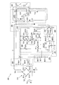
- FIG. 1 shows a circuit diagram of a first embodiment 100 of the power supply device of the present invention.
- the power supply apparatus 100 of this embodiment includes a full-wave rectifier circuit 110 that converts an AC voltage Vac from the AC power supply 10 into a DC voltage Vdc, a power supply circuit 130, a control circuit 140, a power supply circuit 160, and a drive signal output circuit 170.
- the full-wave rectifier circuit 110 has a plurality of diodes D111 to D114 connected in a bridge, full-wave rectifies the AC voltage Vac applied between the AC input terminals a and b, and between the positive terminal c and the negative terminal d.
- a DC voltage Vdc is generated.
- the DC voltage Vdc is a pulsating DC voltage having a magnitude (amplitude) that changes in accordance with the magnitude (amplitude) of the AC voltage Vac.
- the negative terminal d of the full wave rectifier circuit 110 is grounded. For this reason, grounding any of the terminals means connecting the terminal to the negative electrode end d.
- the full-wave rectifier circuit 110 constitutes the “first DC power supply” of the present invention.
- the power supply circuit 130 is disposed between the positive end c and the negative end d of the full-wave rectifier circuit 110 and one end 131 and the other end 132 of the load 120, and supplies DC power to the load 120.
- a capacitor C131 having a capacitance C1 is disposed between one end 131 and the other end 132 of the load 120.
- an inductor L131 having an inductance L1 and an inductor L132 having an inductance L2 are arranged in series. At this time, the inductor L131 is connected to one end 131, and the inductor L132 is connected to the positive end c.
- a switching element T131 is disposed between the other end 132 of the load 120 and the ground.
- an N-type MOSFET is used as the switching element T131.
- a capacitor C132 having a capacitance Cp is arranged between a connection point r between the inductor L131 and the inductor L132 and the ground.
- a diode D131 (freewheeling diode) is disposed between the other end 132 of the load 120 and the connection point r. At this time, the anode of the diode D131 is connected to the other end 132, and the cathode is connected to the connection point r.
- the switching element T131 corresponds to the “first switching element” of the present invention
- the capacitor C131 corresponds to the “first capacitor” of the present invention
- the capacitor C132 corresponds to the “second capacitor” of the present invention
- the inductor L131 corresponds to the “first inductor” of the present invention
- the inductor L132 corresponds to the “second inductor” of the present invention.
- the power supply circuit 160 is disposed between the positive terminal c and the ground, and includes a resistor R161, a Zener diode ZD161, and a capacitor C161.
- the power supply circuit 160 applies a voltage Vzd determined by the Zener voltage of the Zener diode ZD161 to the control circuit 140 and the drive signal output circuit 170.
- the drive signal output circuit 170 is disposed between a connection point (voltage Vzd) between the resistor R161 and the Zener diode ZD161 and the ground, and includes a switch SW171 and resistors R171 and R172. When the switch SW 171 is turned on, the drive signal output circuit 170 outputs an H level drive signal instructing the start of supply of DC power to the load 120 to the clock signal generation circuit 141 of the control circuit 140.
- the control circuit 140 includes a clock signal generation circuit 141 and a drive circuit 142.
- the clock signal generation circuit 141 outputs a clock signal to the input terminal of the drive circuit 142.
- the drive circuit 142 includes switching elements T142a and T142b connected in series between the DC voltage Vzd generated by the power supply circuit 160 and the ground.
- a P-type MOSFET is used as the switching element T142a
- an N-type MOSFET is used as the switching element T142b.
- a connection point (output terminal) between the switching elements 142 a and 142 b is connected to the gate of the switching element T 131 of the power supply circuit 130.
- the drive circuit 142 generates a drive voltage for turning on and off a switching element T131 at an output terminal based on a clock signal input to the input terminal.
- the on period Mon and the off period Moff of T131 are equal to the first period Ka and the second period Kb of the clock signal (including “substantially equal”).
- no component for detecting the current flowing through the switching element T131 is provided, and current detection processing, processing for comparing the detected current with a threshold value, and the like are not performed.
- each element may be represented only by a symbol.
- the switching element T131 that is an N-type MOSFET is represented by “T131”.
- the drive circuit 142 generates an H level drive voltage at the output terminal that turns on the T131 during the first period Ka in which the clock signal is at the H level.
- the current I2 discharge current of the capacitor C132
- the inductor L131 the parallel circuit of the load 120 and the capacitor C131, the path of T131 and the ground due to the charge accumulated in the capacitor C132.
- electromagnetic energy [L1 ⁇ (I2) 2/ 2] is stored in the inductor L131.
- T131 is on, the voltage at the point r becomes lower than Vdc due to the discharge of the capacitor C132. For this reason, the current I1 flows through the full-wave rectifier circuit 110, the inductor L132, the capacitor C132, and the ground path while T131 is on.
- the drive circuit 142 generates an L level drive voltage at the output terminal that turns off T131 during the second period Kb in which the clock signal is at the L level.
- current I3 return current
- the inductor L131 flows through the inductor L131, the parallel circuit of the load 120 and the capacitor C131, and the path of the diode D131 due to the electromagnetic energy accumulated in the inductor L131.
- the current I1 flows through the full-wave rectifier circuit 110, the inductor L132, the capacitor C132, and the ground path. Thereby, the electric charge of the capacitor C132 discharged during the ON period of T131 is replenished.
- the clock signal period M, the inductance L2 of the inductor L132, and the capacitance Cp of the capacitor C132 are set so that the current I1 continues to flow while T131 is off. Details will be described later.
- the current I1 is a current obtained by adding a current component having a magnitude synchronized with the DC voltage (pulsating DC voltage) Vdc and a current component that fluctuates in the control period M.
- the current obtained by adding the current I1 and the current flowing through the power supply circuit 160 is equal to the absolute value of the AC input current Iac.
- Generation of harmonic current is suppressed.
- the low-pass filter 480 used in the conventional power supply apparatus 400 shown in FIG. 6 can be removed. Therefore, the efficiency of the power supply device can be improved and the product shape can be greatly reduced.
- each operation movement of the power supply device 100 of this embodiment is demonstrated.
- Each waveform is shown in FIG. 3 and FIG.
- Each waveform shown in FIGS. 3 and 4 will be described later.
- the charging / discharging operation of the capacitor C132 will be described.
- T131 When T131 is turned on, the capacitor C132 is discharged and the current I2 flows as described above. Since the resistance value of the path through which the current I2 flows is very small, the reached current value (saturation current value) becomes very large, and the current I2 immediately after the rise increases linearly.
- the inter-terminal voltage VL1 of the inductor L131 when the T131 is turned on is expressed by equation (1).
- the VCp decreases due to the discharge of the capacitor C132 during the ON period of T131.
- Capacitor C132 is charged with ( ⁇ Vdc ⁇ Cp) in the process of increasing Vdc, and ( ⁇ Vdc ⁇ Cp) is discharged in the process of decreasing Vdc. Therefore, the charge amount of the capacitor C132 in one control cycle M of T131 (hereinafter referred to as “Cp charge amount”) is expressed by the equation (5).
- Cp charge amount Q1 + ⁇ Vdc ⁇ Cp (5)
- the Cp charge amount can be regarded as being equal to the discharge charge amount Q1.
- the Cp charge amount is supplied by the AC input current Iac.
- the AC input current Iac in the control period M is determined by the discharge charge amount Q1. If the discharge charge amount Q1 is proportional to (Vdc ⁇ VLED), the AC input current Iac is proportional to (Vac ⁇ VLED). That is, if it can be considered that VLED is constant, the AC input current Iac changes in synchronization with the change of the AC voltage Vac.
- I3 at time t1 is I3 (t1)
- I3 can be expressed by equation (7).
- Equation (8) is established. Therefore, equation (7) is rewritten to equation (9).
- T131 is turned on while the return current I3 flows through the diode D131.
- the turn-off current of the diode D131 increases, a large current instantaneously flows through the capacitor C132, the diodes D131, T131, and the ground path, and the capacitor C132 is discharged. Since this current does not flow through the load 120, it causes a reduction in efficiency.
- T131 is turned on while the return current I3 flows, I2 varies due to the return current I3, and the discharge charge amount Q1 of the capacitor C132 varies.
- I1 when T131 is turned off will be described. Assume that T131 shifts from on to off at time t1. Assuming that I1 and VCp at time t1 are I1 (t1) and VCp (t1), respectively, I1 is expressed by equation (11).
- equation (12) is obtained.
- I1 is a waveform in which upward convex waveforms are connected.
- I1 The waveform of I1 will be described (see FIGS. 3 and 4).
- T131 is turned off at time t1
- I1 increases.
- the positive terminal voltage (r-point voltage) VCp of the capacitor C132 increases.
- [Vdc ⁇ VCp] changes due to an increase in VCp
- I1 also changes.
- the inductor L132 acts so that the change of I1 is minimized.
- the gradient of I1 becomes zero, and the gradient becomes the smallest in the region before and after that.
- I1 has a waveform (a part of an upwardly convex sine wave) that becomes maximum at the middle point t3 of the control cycle M starting from the time point t1 and is minimized at both ends of the control cycle M of I1. Even if the waveform of I1 deviates from this waveform due to some disturbance, the waveform of I1 returns to this waveform by the action of the inductor L132.
- the fluctuation width (difference between the maximum value and the minimum value) of the convex waveform of I1 is a ratio of the control period M and the half cycle [ ⁇ (L2 ⁇ Cp) 1/2 ] of the sine wave representing the convex waveform of I1.
- I1 continues to flow as the charging current of the capacitor C132 through the control cycle M of T131.
- the fluctuation width of the convex waveform of I1 becomes smaller and the harmonic component of the AC input current Iac becomes smaller.
- the average value of I1 in the control cycle M is proportional to (Vdc ⁇ VLED).
- an AC input current Iac proportional to (Vdc ⁇ VLED) flows every control cycle M. That is, by fixing the on-period Mon of T131, it is possible to improve the accuracy of charge measurement by the capacitor C132. 3)
- the current I1 that charges the capacitor C132 via the inductor L132 during the off period Moff of T131 is expressed as a half wavelength of a sine wave or a part thereof.
- the average value of I1 for each control cycle M is ideally proportional to Vdc.
- I1 does not flow.
- I1 increases stepwise from zero, so that it is close to the fundamental frequency of the AC input current Iac.
- I1 is proportional to (Vds ⁇ VLED)
- I1 increases smoothly from zero, so that the generation of harmonic components can be suppressed. it can.
- FIG. 2 shows a circuit diagram of the power supply device 200 of the second embodiment.
- the power supply apparatus 200 of the present embodiment is configured by a full-wave rectifier circuit 210, a power supply circuit 230, a control circuit 240, a power supply circuit 260, and a drive signal output circuit 270.
- the control circuit 240 is different from the control circuit 140 of the first embodiment. Therefore, only the configuration of the control circuit 240 will be described below.
- the components given the same reference numerals except the third digit as the reference symbols given to the respective components shown in FIG. 1 are the same components.
- the control circuit 240 includes a clock signal generation circuit 241, a drive circuit 242, and an on period setting circuit 250.
- the clock signal generation circuit 241 and the drive circuit 242 have the same configuration as the clock signal generation circuit 141 and the drive circuit 142 of the control circuit 140 of the first embodiment.
- the clock signal period M of the clock signal generated from the clock signal generation circuit 241 is equal to the control period M of the switching element T231, but the first periods Ka and L in which the clock signal is at the H level.
- the second period Kb which is the level is different from the on period Ma and the off period Mb of the switching element T231.
- the on period setting circuit 250 sets the on period Mon of the switching element T231 based on the clock signal generated from the clock signal generation circuit 241 at a fixed clock signal period M.
- the on-period setting circuit 250 includes switching elements T251 to T257, resistors R251 to R253, variable resistor (volume) R254, capacitor C251, Schmitt trigger ST251, D flip-flop DFF251, AND gate AND251, and inverter INV251.
- P-type MOSFETs are used as the switching elements T251 and T253
- N-type MOSFETs are used as the switching elements T252 and T254 to T257.
- a series circuit of T251, R251, T252, and R252 is arranged between the voltage Vzd generated by the power supply circuit 260 and the ground. In T251 and T252, the gate and the drain are short-circuited.
- a series circuit of T253, T254, and R253 is disposed between Vzd and ground.
- the gate of T253 is connected to the gate of T251, and T251 and T253 form a current mirror circuit.
- the gate of T254 is connected to the gate of T252, and a current mirror circuit is configured by T252 and T254. Further, C251 and T255 are arranged in parallel with R253.
- the output terminal of the AND 251 is connected to the gate of T255 via the INV 251 and to the input terminal of the drive circuit 242.
- the input terminal of the AND 251 is connected to the output terminal of the drive signal output circuit 270, the inverted output terminal ( ⁇ Q) of the DFF 251, and the output terminal of the clock signal generation circuit 241.
- the voltage at the connection point s between the drain of T253 and the drain of T254 is input to the clock terminal (CLK) of the DFF 251 via ST251.
- CLK clock terminal
- the inverted output terminal ( ⁇ Q) becomes the L level.
- the DFF 251 is reset (the inverted output terminal ( ⁇ Q) is at the H level) when the L level clock signal is input to the reset terminal (R bar).
- a series circuit of R254 and T257 is arranged between Vzd and ground. In T257, the gate and the drain are short-circuited. In T256, the gate is connected to the gate of T257, the drain is connected to the coupling point of R251 and T252, and the source is grounded.
- a current mirror circuit is configured by T256 and T257.
- the power supply circuit 260 that generates the set voltage Vzd corresponds to the “second DC power supply” of the present invention.
- connection point between the resistor R261 and the Zener diode ZD261 and the ground corresponds to the “first terminal of the second DC power supply” of the present invention, and the other corresponds to the “second DC power supply of the present invention.
- T251 and T253 correspond to the “first and second P-type MOSFETs” of the present invention
- T252 and T254 correspond to the “first and second N-type MOSFETs” of the present invention
- T255 corresponds to the present
- R251 to R253 correspond to “first to third resistors” of the invention
- C251 corresponds to the “third capacitor” of the invention.
- the current flowing through R251 is I4
- the current flowing through R252 is I5
- the current flowing through T253 and T254 is I6
- the drain current of T256 is I7.
- the channel width of T253 constituting the current mirror circuit with T251 is set larger than the channel width of T251.
- the channel width of T254 constituting the current mirror circuit with T252 is set smaller than the channel width of T252.
- the resistance value of R253 is set to a value inversely proportional to the channel width ratio of T252 and T254 with respect to the resistance value of R252.
- T255 When T255 is turned on in this state, the capacitor C251 is discharged and the source of T254 is grounded. As a result, the gate-source voltage of T254 becomes larger than the gate-source voltage of T252 by (resistance value of R252 ⁇ I5), so that the current that can be passed by T254 increases.
- the channel width of T253 is set larger than the channel width of T251, but I6 that flows when the source of T254 is grounded is set so as not to exceed the maximum current that can be passed by T254 in that state. . Therefore, I6 at this time becomes a saturation current of T253, but becomes an unsaturated current with respect to T254. Therefore, the potential at the point s decreases, and the output signal of ST251 becomes L level.
- the capacitor C251 is charged from the time when the clock signal rises to H level, the potential at the point s becomes the set potential, and the output signal of ST251 changes from L level to H level. This is the period until inversion.
- the potential at the point s in the first period Ka in which the clock signal is at the H level, the potential at the point s is the set potential from the time when the clock signal rises to the H level (the start time of the first period Ka). Thus, it is set so as to exceed the period until the output signal of ST251 is inverted from the L level to the H level.
- the DFF 251 is reset and the inverting output terminal ( ⁇ Q) becomes H level.
- the OFF period Moff of T231 is a period from the time when ST251 is inverted from the L level to the H level until the next clock signal rises to the H level (the start time of the next first period Ka). That is, the on period setting circuit 250 sets the period from the start of the first period Ka of the clock signal until the set time elapses as the on period Mon of T231. Note that the off period Moff of T231 is a period from the elapse of the set time to the start of the next first period Ka.
- the on-period Mon of T231 varies depending on the increasing slope of the source voltage of T254. For this reason, for example, when the capacitance of the capacitor C251 is increased, the increasing slope of the source voltage of T254 becomes gentle, and the on-period Mon of T231 becomes longer.
- the on-period Mon of T231 is proportional to (resistance value of resistance R252 ⁇ I5). For this reason, for example, if I5 is reduced, the ON period Mon of T231 is shortened.
- the drain current I7 of T256 is inversely proportional to the resistance value of the variable resistor R254 disposed between T256 and the drain of T257 constituting the current mirror circuit and Vzd.
- an on period Mon that is shortened by a period corresponding to I7 set by R254 is set with respect to the on period Mon of T231 when I7 is not flowing (the adjustment amount is not set).
- the off period Moff of T231 is extended (lengthened) by the shortened period of the on period Mon compared to the off period Moff when I7 is zero.
- the decreasing rate of the on-period Mon of T231 is slightly larger than the decreasing rate of I5, but the object of shortening the on-period Mon of T231 is achieved.
- shortening (shortening) the ON period Mon of T231 within the fixed control cycle M it is possible to prevent an increase in output due to an increase in the AC voltage Vac.
- the light quantity of LED which is load can be reduced.
- the ON period setting circuit 250 starts from the start of the first period Ka of the clock signal until the set time adjusted by the adjustment amount set by the adjustment amount setting circuit (variable resistor R254) elapses. Is set as the ON period Mon of T231.
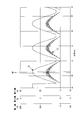
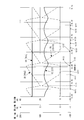
- FIG. 3 The result of having performed the simulation about the power supply device 100 of 1st Embodiment is shown in FIG. 3 and FIG. FIG. 4 is an enlarged view of a portion IV (31 ms to 31.12 ms) in FIG.
- the circuit constants used for the simulation are as follows. Vac: AC100V (effective voltage), 60 Hz, L1: 30 ⁇ H, L2: 600 ⁇ H, Cp: 0.5 ⁇ F, C1: 200 ⁇ F, control cycle (clock signal cycle): 30 ⁇ s (ON period (H level period): 4.509 ⁇ s) VLED average value: 26.3 V, load current average value: 2.92 A.
- the adjustment of the control period M and the ON period Mon within the control period M is performed using an analog circuit, but can also be performed by software using a microcomputer or the like.
- the horizontal axis represents time (unit: ms)
- the first vertical axis (unit: V) represents the voltage of the graph (A)
- the second vertical axis (unit: A) represents the graph.
- (C) represents the current.
- Graph (A) represents DC voltage Vdc
- graph (C) represents current (charging current) I1 supplied from Vdc to capacitor C132.
- FIG. 4 is an enlarged view of a portion IV in FIG. However, a graph (B) (plus terminal voltage VCp of the capacitor C132) and a graph (D) (current (I2 + I3) flowing through the inductor L131) not shown in FIG. 3 are added.
- the voltage value in the graph (B) is represented by the first axis (unit: V) in FIG. 4
- the current value in the graph (D) is represented by the third axis (unit: A) in FIG.
- Vdc can be regarded as a constant value in the enlarged range shown in FIG.
- VCp becomes larger than Vdc in the latter half of the off period Moff (time t1 to time t0) of T131 [VCp> Vdc], and becomes maximum at the end of the off period Moff.
- T131 shifts from OFF to ON (time t0) VCp rapidly decreases along an upwardly convex parabola.
- I1 is a part of the sine wave represented by the equation (12), and has a peak (maximum) at the midpoint (time t3) of the off period Moff (time t1 to time t0) of T131, and T131 changes from on to off. It becomes an upwardly convex waveform that becomes a minimum at the time t1 when the transition is made.
- the reason why the waveform of I1 becomes such a waveform is that, as described above, the inductor L132 acts so that the gradient change is minimized.
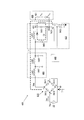
- FIG. 5 shows a circuit diagram of a third embodiment 300 of the power supply device of the present invention.
- the configuration of the power supply circuit 330 is different from the power supply circuit 130 of the first embodiment. Therefore, only the configuration of the power supply circuit 330 will be described below.
- the constituent elements that are the same as those in FIG. 1 except the third digit are the same as the constituent elements used in FIG.
- the power supply circuit 330 includes first and second capacitors C331 and C332, first and second inductors L331 and L332, a diode (freewheel diode) D331, and The first switching element T331 is included.
- an inductor L332 having an inductance L2 and a capacitor C332 having a capacitance Cp are arranged in series between the positive electrode end c and the ground.
- an inductor L331 having an inductance L1 and a switching element T331 are arranged in series.
- a parallel circuit of a capacitor C331 having a capacitance C1 and a load 320 and a series circuit of a diode D331 are arranged in parallel.
- the anode of the diode D331 is connected to the coupling point between the inductor L331 and the switching element T331. For this reason, the polarity of the LED 321 of the load 320 is reversed.
- the discharge charge amount Q1 of the capacitor C332 during the on-period of T331 is expressed by equation (13) by replacing (Vdc ⁇ VLED) in equation (4) with Vdc. Similar to the equation (4), in the equation (13), t1 represents the ON period Mon of T331, Vdc represents the pulsating DC voltage, and L1 represents the inductance of the inductance L331.
- the calculation method of I1 is the same as the calculation method of I1 in FIG. Therefore, also in this embodiment, by setting I3 to disappear within the OFF period Moff of T331, for example, the half cycle [ ⁇ (L2 ⁇ Cp) 1/2 ] of the sine wave of I1 is controlled by the control cycle M.
- Stable PFC control can be realized by setting the inductance L2 of the inductor L332 and the capacitance Cp of the capacitor C332 so as to be longer.
- the power supply circuit 130 of the first embodiment operates as a buck converter
- the power supply circuit 330 of the third embodiment operates as a buck-boost converter.
- the power supply circuit 330 of the third embodiment has the following characteristics with respect to the power supply circuit 130 of the first embodiment.
- the discharge charge amount Q1 in the first embodiment depends on (Vdc ⁇ VLED) as expressed by the equation (4). For this reason, when the VLED changes, the discharge charge amount Q1 also changes accordingly.
- the discharge charge amount Q1 in the third embodiment does not include the VLED as represented by the equation (13). For this reason, stable PFC control can be realized without being affected by fluctuations in VLED.
- I1 does not flow in the range of [Vdc ⁇ VLED].
- there is no restriction for this reason, even when Vdc falls, I1 flows (the range in which I1 flows increases). This contributes to suppression of the harmonic component of I1.
- the parallel circuit of the inductor L131 (L231), the load 120 (220), and the capacitor C131 (C231) is connected in series. For this reason, even if the position of the parallel circuit of the inductor L131 (L231), the load 120 (220), and the capacitor C131 (C231) is changed, the obtained effect does not change.
- a DC power source having a full-wave rectifier circuit that converts an AC voltage into a pulsating DC voltage obtained by full-wave rectification is used, but a battery or the like is used as a DC power source.
- a DC power source such as a battery can be regarded as a DC power source that generates a pulsating DC voltage having an infinite period.
- a battery or the like is used as a DC power supply, it is not necessary to consider the phase shift (power factor) of the AC input current with respect to the AC voltage as in the case of using a DC power supply having a full-wave rectifier. It has the effect of suppressing harmonic components contained in the supplied current. Therefore, there is an effect that it is possible to remove or downsize the low-pass filter for suppressing the harmonic component, and an effect that the component for detecting the current flowing through the switching element and the current detection processing can be made unnecessary.
- a DC power source such as a battery corresponds to the “third DC power source” of the present invention.
- the present invention is not limited to the configuration described in the detailed description, and various modifications, additions, and deletions can be made without departing from the gist of the present invention.
- the power supply apparatus of the present invention can supply DC power to various loads other than the light emitting diode.
- the values (for example, inductance, capacitance, resistance value) of elements constituting each circuit can be appropriately set according to the type of load.
- the switching element for supplying power to the load an FET is preferably used, but an element other than the FET can also be used.
- the switching element is turned on when the clock signal is at the H level, and is turned off when the clock signal is at the L level. It can also be configured to turn off.
- DESCRIPTION OF SYMBOLS 10 ... AC power supply, 100, 200, 300, 400 ... Power supply device, 110, 210, 310, 410 ... Full wave rectifier circuit, 120, 220, 320, 420 ... Load, 121, 221, 321, 421 ... Light emitting diode ( LED), 130, 230, 330, 430 ... power supply circuit, 140, 240, 340, 440 ... control circuit, 141, 241, 341 ... clock signal generation circuit, 142, 242, 342 ... drive circuit, 160, 260, 360 ... Power supply circuit, 170, 270, 370 ... Drive signal output circuit, 250 ... On period setting circuit, 480 ...
- Low pass filter L131, L132, L231, L232, L331, L332, L431, L481, L482 ...
- Inductor C131, C132, C231, C232, C251, C331, C332 C431, C481, C482 ... capacitor, D131, D231, D331, D431 ... freewheeling diode, T131, T231, T255, T331, T431 ... switching device, R254 ... variable resistor (adjustment amount setting circuit).
Landscapes
- Engineering & Computer Science (AREA)
- Power Engineering (AREA)
- Dc-Dc Converters (AREA)
- Rectifiers (AREA)
Abstract
L'invention aborde le problème de réaliser, de manière peu coûteuse et par l'intermédiaire d'une configuration simple, un dispositif d'alimentation électrique qui est capable d'améliorer le rendement. L'invention réalise à cet effet un circuit redresseur pleine onde (110) qui génère une tension continue (tension CC pulsée) Vdc pour laquelle une tension alternative Vac a été redressée. Un élément de commutation (T131) qui constitue une partie d'un circuit d'alimentation électrique (130) est rendu passant pendant une période d'activation fixée Mon, et bloqué pendant une période de désactivation fixée Moff (= M - Mon) pour des cycles de commande fixe individuels M. Lorsque l'élément de commutation (T131) est passant, la charge stockée dans un condensateur (C132) amène un courant (I2) à circuler sur un trajet comprenant une inductance (L131) et l'élément de commutation. Lorsque l'élément de commutation (T131) est bloqué, l'énergie électromagnétique stockée dans l'inductance (L131) produit un courant de retour (I3) qui circule à travers une diode (D131) et les circuits parallèles constitués d'un condensateur (C131) et d'une charge (120). Simultanément, un courant (I1) est délivré au condensateur (C132) par le circuit redresseur pleine onde (110) par le biais d'une inductance (L132). Une configuration est adoptée de telle sorte que le courant (I1) continue de circuler vers le condensateur (C132) pendant la période où l'élément de commutation (T131) est bloqué.
Priority Applications (3)
| Application Number | Priority Date | Filing Date | Title |
|---|---|---|---|
| PCT/JP2016/053542 WO2017134824A1 (fr) | 2016-02-05 | 2016-02-05 | Dispositif d'alimentation électrique |
| JP2017565374A JP6635439B2 (ja) | 2016-02-05 | 2016-02-05 | 電源装置 |
| US16/073,515 US10312804B2 (en) | 2016-02-05 | 2016-02-05 | Power supply apparatus with power factor correction using fixed on and off periods |
Applications Claiming Priority (1)
| Application Number | Priority Date | Filing Date | Title |
|---|---|---|---|
| PCT/JP2016/053542 WO2017134824A1 (fr) | 2016-02-05 | 2016-02-05 | Dispositif d'alimentation électrique |
Publications (1)
| Publication Number | Publication Date |
|---|---|
| WO2017134824A1 true WO2017134824A1 (fr) | 2017-08-10 |
Family
ID=59500623
Family Applications (1)
| Application Number | Title | Priority Date | Filing Date |
|---|---|---|---|
| PCT/JP2016/053542 Ceased WO2017134824A1 (fr) | 2016-02-05 | 2016-02-05 | Dispositif d'alimentation électrique |
Country Status (3)
| Country | Link |
|---|---|
| US (1) | US10312804B2 (fr) |
| JP (1) | JP6635439B2 (fr) |
| WO (1) | WO2017134824A1 (fr) |
Cited By (1)
| Publication number | Priority date | Publication date | Assignee | Title |
|---|---|---|---|---|
| JPWO2021070279A1 (fr) * | 2019-10-09 | 2021-04-15 |
Families Citing this family (4)
| Publication number | Priority date | Publication date | Assignee | Title |
|---|---|---|---|---|
| WO2018172565A1 (fr) | 2017-03-24 | 2018-09-27 | Ambu A/S | Partie de pointe articulée destinée à un endoscope |
| EP3706299A4 (fr) * | 2018-02-21 | 2021-06-23 | Tae Jun Yoon | Dispositif de redressement ayant une fonction de réduction d'énergie fantôme |
| US11418125B2 (en) | 2019-10-25 | 2022-08-16 | The Research Foundation For The State University Of New York | Three phase bidirectional AC-DC converter with bipolar voltage fed resonant stages |
| CN116865215B (zh) * | 2023-08-30 | 2024-09-03 | 珠海汇众能源科技有限公司 | 一种并联断路器电路 |
Citations (5)
| Publication number | Priority date | Publication date | Assignee | Title |
|---|---|---|---|---|
| JPH09201043A (ja) * | 1996-01-12 | 1997-07-31 | Canon Inc | 電源装置 |
| JP2011078261A (ja) * | 2009-10-01 | 2011-04-14 | Panasonic Corp | 電流駆動回路 |
| JP2011091974A (ja) * | 2009-10-26 | 2011-05-06 | Cosel Co Ltd | スイッチング電源装置 |
| JP2012226924A (ja) * | 2011-04-18 | 2012-11-15 | Panasonic Corp | 半導体発光素子の点灯装置およびそれを用いた照明器具 |
| US20130314961A1 (en) * | 2012-05-25 | 2013-11-28 | Fairchild Korea Semiconductor Ltd. | Switch control device, power supply device comprising the same, and driving method of power supply device |
Family Cites Families (48)
| Publication number | Priority date | Publication date | Assignee | Title |
|---|---|---|---|---|
| US4430608A (en) | 1981-12-22 | 1984-02-07 | Hughes Aircraft Company | Base drive circuit |
| US4890009A (en) | 1987-04-30 | 1989-12-26 | Hitachi, Ltd. | Monolithic integrated circuit device |
| GB2207315B (en) | 1987-06-08 | 1991-08-07 | Philips Electronic Associated | High voltage semiconductor with integrated low voltage circuitry |
| US4937697A (en) | 1989-05-22 | 1990-06-26 | Motorola, Inc. | Semiconductor device protection circuit |
| US5783915A (en) | 1995-01-20 | 1998-07-21 | Matsushita Electric Industrial Co., Ltd. | Linear actuating apparatus |
| CN1080941C (zh) | 1996-08-29 | 2002-03-13 | 罗姆股份有限公司 | 供电装置 |
| IT1286047B1 (it) | 1996-10-25 | 1998-07-07 | Abb Research Ltd | Sistema di distribuzione dell'energia elettrica con interruttori automatici di protezione e relativo procedimento |
| US5998981A (en) | 1997-06-03 | 1999-12-07 | International Business Machines Corporation | Weak inversion NMOS regulator with boosted gate |
| JP3706515B2 (ja) | 1998-12-28 | 2005-10-12 | 矢崎総業株式会社 | 電源供給制御装置および電源供給制御方法 |
| JP2001216033A (ja) | 2000-02-02 | 2001-08-10 | Yazaki Corp | 電源供給制御装置および電源供給制御方法 |
| JP3741949B2 (ja) | 2000-07-24 | 2006-02-01 | 矢崎総業株式会社 | 半導体スイッチング装置 |
| JP3914004B2 (ja) | 2001-05-25 | 2007-05-16 | 矢崎総業株式会社 | 半導体素子の過電流検出・保護装置 |
| JP3767445B2 (ja) | 2001-09-28 | 2006-04-19 | アンデン株式会社 | 過電流保護機能を有する電源供給装置、負荷駆動装置および車両用電源供給装置 |
| US6901212B2 (en) | 2002-06-13 | 2005-05-31 | Halliburton Energy Services, Inc. | Digital adaptive sensorless commutational drive controller for a brushless DC motor |
| JP3990218B2 (ja) | 2002-07-12 | 2007-10-10 | 矢崎総業株式会社 | 半導体素子の保護装置 |
| JP3842205B2 (ja) | 2002-11-19 | 2006-11-08 | 矢崎総業株式会社 | パワーウインドの駆動装置 |
| JP4344569B2 (ja) | 2003-09-08 | 2009-10-14 | 矢崎総業株式会社 | パワーウインドの駆動装置 |
| JP3964375B2 (ja) | 2003-09-30 | 2007-08-22 | 矢崎総業株式会社 | パワーウインドの駆動装置 |
| JP4003833B2 (ja) | 2003-10-06 | 2007-11-07 | オリジン電気株式会社 | 電界制御型半導体素子の駆動回路 |
| JP4056961B2 (ja) | 2003-10-16 | 2008-03-05 | 矢崎総業株式会社 | パワーウインドの駆動装置 |
| US7542258B2 (en) | 2004-01-16 | 2009-06-02 | Lutron Electronics Co., Inc. | DV/dt-detecting overcurrent protection circuit for power supply |
| JP4278572B2 (ja) | 2004-06-16 | 2009-06-17 | 矢崎総業株式会社 | 半導体スイッチの制御装置 |
| JP4398312B2 (ja) | 2004-07-06 | 2010-01-13 | 矢崎総業株式会社 | 半導体スイッチの制御装置 |
| JP2006060971A (ja) | 2004-08-23 | 2006-03-02 | Yazaki Corp | 半導体スイッチの制御装置 |
| JP4504222B2 (ja) | 2005-02-21 | 2010-07-14 | 矢崎総業株式会社 | 過電流検出装置 |
| JP4713963B2 (ja) | 2005-07-07 | 2011-06-29 | 矢崎総業株式会社 | 過電流検出装置 |
| JP4701052B2 (ja) | 2005-09-21 | 2011-06-15 | 矢崎総業株式会社 | 過電流検出装置 |
| JP4643419B2 (ja) | 2005-11-08 | 2011-03-02 | 矢崎総業株式会社 | 自己診断機能を備えた負荷駆動装置 |
| JP4776368B2 (ja) | 2005-12-20 | 2011-09-21 | 矢崎総業株式会社 | 電力供給回路のオン故障検出装置 |
| JP4929020B2 (ja) | 2007-04-10 | 2012-05-09 | 矢崎総業株式会社 | 負荷回路の過電流保護装置 |
| JP4943939B2 (ja) | 2007-05-14 | 2012-05-30 | 矢崎総業株式会社 | 過電流保護装置 |
| JP5030717B2 (ja) | 2007-09-10 | 2012-09-19 | 矢崎総業株式会社 | 過電流保護装置 |
| JP5087441B2 (ja) | 2008-03-19 | 2012-12-05 | 矢崎総業株式会社 | 電力供給装置 |
| JP5171402B2 (ja) | 2008-06-04 | 2013-03-27 | 矢崎総業株式会社 | 負荷回路の過電流保護装置 |
| JP5171406B2 (ja) | 2008-06-05 | 2013-03-27 | 矢崎総業株式会社 | 負荷回路の過電流保護装置 |
| JP5185021B2 (ja) | 2008-08-26 | 2013-04-17 | 矢崎総業株式会社 | 負荷回路の保護装置 |
| JP5370090B2 (ja) | 2009-11-12 | 2013-12-18 | アンデン株式会社 | 過電流検出機能を有したスイッチ回路 |
| JP5406802B2 (ja) | 2010-08-05 | 2014-02-05 | 矢崎総業株式会社 | 負荷制御装置 |
| US8928297B2 (en) * | 2011-01-31 | 2015-01-06 | Infineon Technologies Austria Ag | Ćuk based current source |
| US8659271B2 (en) * | 2011-03-23 | 2014-02-25 | Grenergy Opto Inc. | Fixed-on-time controller utilizing an adaptive saw signal for discontinuous mode PFC power conversion |
| JP2012227845A (ja) | 2011-04-21 | 2012-11-15 | Shunzo Oshima | 過電流保護電源装置 |
| JP2012235398A (ja) | 2011-05-08 | 2012-11-29 | Shunzo Oshima | 過電流保護電源装置 |
| US8569963B2 (en) * | 2011-06-17 | 2013-10-29 | Intersil Americas Inc. | Cascade boost and inverting buck converter with independent control |
| US9257901B2 (en) * | 2012-02-09 | 2016-02-09 | Panasonic Intellectual Property Management Co., Ltd. | DC power supply circuit |
| EP2846464B1 (fr) | 2012-05-01 | 2019-01-09 | Shunzou Ohshima | Appareil d'alimentation électrique avec protection contre les surintensités |
| JP2014054157A (ja) | 2012-09-10 | 2014-03-20 | Shunzo Oshima | 過電流保護電源装置 |
| US20150012362A1 (en) | 2013-07-03 | 2015-01-08 | 1-800 Contacts, Inc. | Systems and methods for recommending products via crowdsourcing and detecting user characteristics |
| JP6429148B2 (ja) * | 2014-11-20 | 2018-11-28 | パナソニックIpマネジメント株式会社 | 点灯装置およびそれを用いた照明器具 |
-
2016
- 2016-02-05 JP JP2017565374A patent/JP6635439B2/ja not_active Expired - Fee Related
- 2016-02-05 WO PCT/JP2016/053542 patent/WO2017134824A1/fr not_active Ceased
- 2016-02-05 US US16/073,515 patent/US10312804B2/en not_active Expired - Fee Related
Patent Citations (5)
| Publication number | Priority date | Publication date | Assignee | Title |
|---|---|---|---|---|
| JPH09201043A (ja) * | 1996-01-12 | 1997-07-31 | Canon Inc | 電源装置 |
| JP2011078261A (ja) * | 2009-10-01 | 2011-04-14 | Panasonic Corp | 電流駆動回路 |
| JP2011091974A (ja) * | 2009-10-26 | 2011-05-06 | Cosel Co Ltd | スイッチング電源装置 |
| JP2012226924A (ja) * | 2011-04-18 | 2012-11-15 | Panasonic Corp | 半導体発光素子の点灯装置およびそれを用いた照明器具 |
| US20130314961A1 (en) * | 2012-05-25 | 2013-11-28 | Fairchild Korea Semiconductor Ltd. | Switch control device, power supply device comprising the same, and driving method of power supply device |
Cited By (3)
| Publication number | Priority date | Publication date | Assignee | Title |
|---|---|---|---|---|
| JPWO2021070279A1 (fr) * | 2019-10-09 | 2021-04-15 | ||
| WO2021070279A1 (fr) * | 2019-10-09 | 2021-04-15 | 三菱電機株式会社 | Dispositif de conversion de courant |
| JP7183445B2 (ja) | 2019-10-09 | 2022-12-05 | 三菱電機株式会社 | 電力変換装置 |
Also Published As
| Publication number | Publication date |
|---|---|
| JP6635439B2 (ja) | 2020-01-29 |
| US20190044439A1 (en) | 2019-02-07 |
| US10312804B2 (en) | 2019-06-04 |
| JPWO2017134824A1 (ja) | 2018-12-06 |
Similar Documents
| Publication | Publication Date | Title |
|---|---|---|
| US9455623B2 (en) | Power factor correction circuit and method | |
| US10236774B2 (en) | Control module for a constant-frequency switching converter and method for controlling a switching converter | |
| CN102656787B (zh) | 开关电源电路和功率因数控制器 | |
| US9837898B2 (en) | Peak-value current mode control for power converters | |
| US8493757B2 (en) | AC/DC converter with a PFC and a DC/DC converter | |
| KR100796890B1 (ko) | 스위칭 전원장치 | |
| JP6635439B2 (ja) | 電源装置 | |
| US8488346B2 (en) | Power conversion apparatus and method | |
| JP2009142085A (ja) | エネルギー伝達装置およびエネルギー伝達制御用半導体装置 | |
| JP6895502B2 (ja) | 調光回路及び調光制御方法 | |
| CN109643957A (zh) | 开关电源装置以及半导体装置 | |
| JP2017070192A (ja) | スイッチング電源装置及びled点灯回路 | |
| KR101183493B1 (ko) | 직류전원장치 | |
| TW202420715A (zh) | 多模式功率因數校正電路及其控制方法 | |
| US9973078B2 (en) | Power conversion apparatus and method of using the apparatus | |
| JP2012070556A (ja) | 直流電源装置 | |
| US20170110981A1 (en) | Power Conversion Method and Power Converter | |
| JP5937597B2 (ja) | スイッチング電源装置 | |
| JP4111326B2 (ja) | スイッチング電源装置 | |
| Shin et al. | Modeling and implementation of digital control for critical conduction mode power factor correction rectifier | |
| CN107196528A (zh) | 开关电源装置的控制方法和控制电路 | |
| CN111049387B (zh) | 一种tlcⅱ型谐振电路及其应用的电源变换器 | |
| CN111245225B (zh) | 一种电源变换系统及其控制电路和电流调节方法 | |
| KR20140001084A (ko) | 공용코어 역률보정 공진 컨버터 | |
| TWI487263B (zh) | 降壓式交直流轉換器 |
Legal Events
| Date | Code | Title | Description |
|---|---|---|---|
| 121 | Ep: the epo has been informed by wipo that ep was designated in this application |
Ref document number: 16889310 Country of ref document: EP Kind code of ref document: A1 |
|
| DPE1 | Request for preliminary examination filed after expiration of 19th month from priority date (pct application filed from 20040101) | ||
| WWE | Wipo information: entry into national phase |
Ref document number: 2017565374 Country of ref document: JP |
|
| NENP | Non-entry into the national phase |
Ref country code: DE |
|
| 122 | Ep: pct application non-entry in european phase |
Ref document number: 16889310 Country of ref document: EP Kind code of ref document: A1 |