WO2017138632A1 - Dispositif électroluminescent - Google Patents
Dispositif électroluminescent Download PDFInfo
- Publication number
- WO2017138632A1 WO2017138632A1 PCT/JP2017/004915 JP2017004915W WO2017138632A1 WO 2017138632 A1 WO2017138632 A1 WO 2017138632A1 JP 2017004915 W JP2017004915 W JP 2017004915W WO 2017138632 A1 WO2017138632 A1 WO 2017138632A1
- Authority
- WO
- WIPO (PCT)
- Prior art keywords
- light
- emitting device
- optical filter
- light emitting
- region
- Prior art date
- Legal status (The legal status is an assumption and is not a legal conclusion. Google has not performed a legal analysis and makes no representation as to the accuracy of the status listed.)
- Ceased
Links
Images


Classifications
-
- H—ELECTRICITY
- H10—SEMICONDUCTOR DEVICES; ELECTRIC SOLID-STATE DEVICES NOT OTHERWISE PROVIDED FOR
- H10K—ORGANIC ELECTRIC SOLID-STATE DEVICES
- H10K59/00—Integrated devices, or assemblies of multiple devices, comprising at least one organic light-emitting element covered by group H10K50/00
- H10K59/10—OLED displays
- H10K59/12—Active-matrix OLED [AMOLED] displays
- H10K59/122—Pixel-defining structures or layers, e.g. banks
-
- G—PHYSICS
- G02—OPTICS
- G02B—OPTICAL ELEMENTS, SYSTEMS OR APPARATUS
- G02B5/00—Optical elements other than lenses
- G02B5/20—Filters
- G02B5/22—Absorbing filters
-
- H—ELECTRICITY
- H05—ELECTRIC TECHNIQUES NOT OTHERWISE PROVIDED FOR
- H05B—ELECTRIC HEATING; ELECTRIC LIGHT SOURCES NOT OTHERWISE PROVIDED FOR; CIRCUIT ARRANGEMENTS FOR ELECTRIC LIGHT SOURCES, IN GENERAL
- H05B33/00—Electroluminescent light sources
- H05B33/02—Details
- H05B33/04—Sealing arrangements, e.g. against humidity
-
- H—ELECTRICITY
- H05—ELECTRIC TECHNIQUES NOT OTHERWISE PROVIDED FOR
- H05B—ELECTRIC HEATING; ELECTRIC LIGHT SOURCES NOT OTHERWISE PROVIDED FOR; CIRCUIT ARRANGEMENTS FOR ELECTRIC LIGHT SOURCES, IN GENERAL
- H05B33/00—Electroluminescent light sources
- H05B33/12—Light sources with substantially two-dimensional [2D] radiating surfaces
- H05B33/22—Light sources with substantially two-dimensional [2D] radiating surfaces characterised by the chemical or physical composition or the arrangement of auxiliary dielectric or reflective layers
-
- H—ELECTRICITY
- H10—SEMICONDUCTOR DEVICES; ELECTRIC SOLID-STATE DEVICES NOT OTHERWISE PROVIDED FOR
- H10K—ORGANIC ELECTRIC SOLID-STATE DEVICES
- H10K50/00—Organic light-emitting devices
-
- H—ELECTRICITY
- H10—SEMICONDUCTOR DEVICES; ELECTRIC SOLID-STATE DEVICES NOT OTHERWISE PROVIDED FOR
- H10K—ORGANIC ELECTRIC SOLID-STATE DEVICES
- H10K50/00—Organic light-emitting devices
- H10K50/10—OLEDs or polymer light-emitting diodes [PLED]
- H10K50/11—OLEDs or polymer light-emitting diodes [PLED] characterised by the electroluminescent [EL] layers
-
- H—ELECTRICITY
- H10—SEMICONDUCTOR DEVICES; ELECTRIC SOLID-STATE DEVICES NOT OTHERWISE PROVIDED FOR
- H10K—ORGANIC ELECTRIC SOLID-STATE DEVICES
- H10K59/00—Integrated devices, or assemblies of multiple devices, comprising at least one organic light-emitting element covered by group H10K50/00
- H10K59/10—OLED displays
- H10K59/17—Passive-matrix OLED displays
- H10K59/173—Passive-matrix OLED displays comprising banks or shadow masks
-
- H—ELECTRICITY
- H10—SEMICONDUCTOR DEVICES; ELECTRIC SOLID-STATE DEVICES NOT OTHERWISE PROVIDED FOR
- H10K—ORGANIC ELECTRIC SOLID-STATE DEVICES
- H10K59/00—Integrated devices, or assemblies of multiple devices, comprising at least one organic light-emitting element covered by group H10K50/00
- H10K59/30—Devices specially adapted for multicolour light emission
- H10K59/38—Devices specially adapted for multicolour light emission comprising colour filters or colour changing media [CCM]
-
- G—PHYSICS
- G02—OPTICS
- G02B—OPTICAL ELEMENTS, SYSTEMS OR APPARATUS
- G02B5/00—Optical elements other than lenses
- G02B5/20—Filters
- G02B5/201—Filters in the form of arrays
Definitions
- the present invention relates to a light emitting device.
- This light-emitting device is used as a lighting device or a display device, and has a configuration in which an organic layer is sandwiched between a first electrode and a second electrode.
- a transparent material is used for the first electrode
- a metal material is used for the second electrode.
- Patent Document 1 One of light-emitting devices using organic EL is a technique described in Patent Document 1.
- the second electrode is provided only in a part of the pixel so that the display device using the organic EL has light transmittance (see-through).
- the display device since the region positioned between the plurality of second electrodes transmits light, the display device can have light transmittance.
- a light-transmitting insulating film is formed between the plurality of second electrodes in order to define pixels.
- Patent Document 1 exemplifies inorganic materials such as silicon oxide and resin materials such as acrylic resin as the material of the insulating film.
- an optical filter may be stacked on the light emitting device.
- an optical filter is provided in a light-emitting device having translucency, the translucency is lowered.
- an example is to make the peak of the emission spectrum steep and prevent the translucency of the light-emitting device from being lowered.
- the invention according to claim 1 is a translucent substrate;
- the first surface of the substrate is provided apart from each other, and has a translucent first electrode, a light reflective second electrode, and an organic layer positioned between the first electrode and the second electrode.
- a plurality of light emitting units A light-transmitting region that is located between the light-emitting portions and transmits light in the thickness direction;
- An optical filter provided on the light emission surface of the substrate, overlapping the light emitting portion and not overlapping at least part of the light transmitting region; It is a light-emitting device provided with.
- FIG. 6 is a cross-sectional view illustrating a configuration of a light emitting device according to Modification Example 1.
- FIG. 12 is a cross-sectional view illustrating a configuration of a light emitting device according to Modification 2.
- FIG. 11 is a cross-sectional view illustrating a configuration of a light emitting device according to Modification 3. It is sectional drawing which shows the structure of the light-emitting device which concerns on the modification 4. It is sectional drawing which shows the structure of the light-emitting device which concerns on the modification of FIG. It is sectional drawing for demonstrating the usage method of the light-emitting device which concerns on an Example.
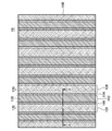
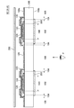
- FIG. 1 is a cross-sectional view illustrating a configuration of a light emitting device 10 according to the embodiment.
- FIG. 2 is a plan view of the light emitting device 10.
- FIG. 1 corresponds to the AA cross section of FIG.
- the light emitting device 10 according to the embodiment includes a light transmissive substrate 100, a plurality of light emitting units 140, light transmissive regions (second region 104 and third region 106), and a first optical filter 200.
- the plurality of light emitting units 140 are provided on the first surface 100a of the substrate 100 and are separated from each other.
- the light emitting unit 140 includes a translucent first electrode 110, an organic layer 120, and a light reflective second electrode 130.
- the organic layer 120 is located between the first electrode 110 and the second electrode 130.
- the light transmitting region is located between the light emitting units 140 and transmits light in the thickness direction of the light emitting device 10.
- the first optical filter 200 overlaps the light emitting unit 140 and does not overlap at least a part of the light transmitting region. In the example shown in the drawing, the first optical filter 200 is provided on the second surface 100 b of the substrate 100. Details will be described below.
- the substrate 100 is a light-transmitting substrate such as a glass substrate or a resin substrate.
- the substrate 100 may have flexibility. In the case of flexibility, the thickness of the substrate 100 is, for example, not less than 10 ⁇ m and not more than 1000 ⁇ m.
- the substrate 100 is, for example, a polygon such as a rectangle or a circle.
- the substrate 100 is formed using, for example, PEN (polyethylene naphthalate), PES (polyethersulfone), PET (polyethylene terephthalate), or polyimide.
- an inorganic barrier film such as SiN x or SiON is formed on at least one surface (preferably both surfaces) of the substrate 100 in order to prevent moisture from permeating the substrate 100. It is preferable.
- the substrate 100 is formed of a resin substrate
- the first electrode 110 and the organic layer 120 described later are directly formed on the resin substrate, and after the first electrode 110 and subsequent layers are formed on the glass substrate. There is a method in which the first electrode 110 and the glass substrate are peeled, and the peeled laminate is disposed on a resin substrate.
- a light emitting unit 140 is formed on one surface of the substrate 100.
- the light emitting unit 140 has a configuration in which a first electrode 110, an organic layer 120 including a light emitting layer, and a second electrode 130 are stacked in this order.
- the plurality of light emitting units 140 extend in a line shape (for example, a straight line shape).
- the plurality of light emitting units 140 preferably extend in parallel to each other.
- the plurality of light emitting units 140 are arranged so as to form a matrix, or form a segment or display a predetermined shape (for example, display an icon). It may be.
- the plurality of light emitting units 140 are formed for each pixel.
- the first electrode 110 is a transparent electrode having optical transparency.
- the material of the transparent electrode is a metal-containing material, for example, a metal oxide such as ITO (Indium Tin Oxide), IZO (Indium Zinc Oxide), IWZO (Indium Tungsten Zinc Oxide), or ZnO (Zinc Oxide).
- the thickness of the first electrode 110 is, for example, not less than 10 nm and not more than 500 nm.
- the first electrode 110 is formed using, for example, a sputtering method or a vapor deposition method.
- the first electrode 110 may be a carbon nanotube or a conductive organic material such as PEDOT / PSS.
- the first electrode 110 may have a stacked structure in which a plurality of films are stacked. In the drawing, a plurality of linear first electrodes 110 are formed on a substrate 100 in parallel with each other. For this reason, the first electrode 110 is not located in the second region 104 and the third region 106.
- the organic layer 120 has a light emitting layer.
- the organic layer 120 has a configuration in which, for example, a hole injection layer, a light emitting layer, and an electron injection layer are stacked in this order.
- a hole transport layer may be formed between the hole injection layer and the light emitting layer.
- an electron transport layer may be formed between the light emitting layer and the electron injection layer.
- the organic layer 120 may be formed by a vapor deposition method.
- at least one layer of the organic layer 120 for example, a layer in contact with the first electrode 110, may be formed by a coating method such as an inkjet method, a printing method, or a spray method. In this case, the remaining layers of the organic layer 120 are formed by vapor deposition.
- all the layers of the organic layer 120 may be formed using the apply
- the emission color of the light emitting layer (or the color of light emitted from the organic layer 120) is different from the emission color of the light emitting layer of the adjacent light emitting unit 140 (or the color of light emitted from the organic layer 120). May be the same or the same.
- the second electrode 130 is made of, for example, a metal selected from the first group consisting of Al, Au, Ag, Pt, Mg, Sn, Zn, and In, or an alloy of a metal selected from the first group. Contains a metal layer. For this reason, the second electrode 130 has a light shielding property or a light reflecting property.
- the thickness of the second electrode 130 is, for example, not less than 10 nm and not more than 500 nm.
- the second electrode 130 is formed using, for example, a sputtering method or a vapor deposition method. In the example shown in this drawing, the light emitting device 10 has a plurality of linear second electrodes 130. The second electrode 130 is provided for each of the first electrodes 110 and is wider than the first electrode 110.
- the entire first electrode 110 is overlapped and covered by the second electrode 130 in the width direction.
- the extraction direction of light emitted from the light emitting layer of the organic layer 120 can be adjusted. Specifically, light emission to the first surface 100a side of the light emitting device 10 can be suppressed.
- the first electrode 110 is wider than the second electrode 130, and when viewed from a direction perpendicular to the substrate 100, the entire second electrode 130 is covered with the first electrode 110 in the width direction. Also good. In this case, the amount of light emitted in the direction where the second electrode 130 of the light emitting device 10 is formed is relatively large.
- the edge of the first electrode 110 is covered with an insulating film 150.
- the insulating film 150 is made of, for example, a photosensitive resin material such as polyimide, and surrounds a portion of the first electrode 110 that becomes the light emitting portion 140. In other words, the insulating film 150 defines the light emitting portion 140. Although the insulating film 150 has a light-transmitting property, the light-transmitting property does not have to be high.
- An edge in the width direction of the second electrode 130 is located on the insulating film 150. In other words, when viewed from a direction perpendicular to the direction in which the light emitting portion 140 extends, a part of the insulating film 150 protrudes from the second electrode 130.
- the organic layer 120 is also formed on the top and side surfaces of the insulating film 150.
- the light emitting device 10 When viewed from a direction perpendicular to the direction in which the light emitting unit 140 extends (that is, the cross-sectional view of FIG. 1), the light emitting device 10 includes a first region 102, a second region 104, and a third region 106. Yes.
- the first region 102 is a region overlapping with the second electrode 130. That is, the first region 102 is a region covered with the second electrode 130 when viewed from the direction perpendicular to the substrate 100, and is the same width as the light emitting unit 140 or wider than the light emitting unit 140. In the example shown in the drawing, the width of the first region 102 is wider than the width of the light emitting unit 140.
- the first region 102 is a region that does not transmit light from the front surface to the back surface of the light emitting device 10 or the substrate 100 and from the back surface to the front surface.
- region located between the 2nd electrodes 130 is a translucent area
- This translucent area is constituted by a second area 104 (first translucent area) and a third area 106 (second translucent area).
- the second region 104 is a region including the insulating film 150 in the light transmitting region.
- the third region 106 is a region that does not include the insulating film 150 in the light transmitting region. The light transmittance of the third region 106 is higher than the light transmittance of the second region 104.
- the width of the second region 104 is narrower than the width of the third region 106. For this reason, the light-emitting device 10 has sufficient light transmittance.
- the width of the third region 106 may be wider or narrower than that of the first region 102.
- the width of the first region 102 is 1, the width of the second region 104 is, for example, 0 or more (or more than 0 or 0.1 or more) 0.2 or less, and the width of the third region 106 is, for example, 0.3. It is 2 or less.
- the width of the first region 102 is, for example, 50 ⁇ m or more and 500 ⁇ m or less
- the width of the second region 104 is, for example, 0 ⁇ m or more (or more than 0 ⁇ m)
- the width of the third region 106 is, for example, 15 ⁇ m or more and 1000 ⁇ m or less. is there.
- the organic layer 120 is continuously formed in the first region 102, the second region 104, and the third region 106.
- the organic layers 120 of the plurality of light emitting units 140 are formed continuously. In this way, it is not necessary to use a mask when forming a continuous layer of the organic layer 120, so that the manufacturing cost of the organic layer 120 can be reduced.
- the organic layer 120 may not be formed in the third region 106. In addition, the organic layer 120 may not be formed in the second region 104.
- the light emitting unit 140 may have a lattice shape.
- the third region 106 is a region surrounded by the second electrode 130 in the substrate 100.
- the light emitting device 10 further includes a first optical filter 200.
- the first optical filter 200 filters a part of the light emitted from the light emitting unit 140.
- the first optical filter 200 is, for example, a color filter for steepening the peak of the emission spectrum of the light emitting unit 140 (in other words, for clearing the emission color of the light emitting unit 140).
- the peak wavelength of the transmission spectrum of the first optical filter 200 is included in the emission spectrum of the light emitting unit 140.
- the first optical filter 200 is a red filter that transmits red light and does not drop light of other colors.
- the first optical filter 200 is a green filter that transmits green light and does not drop light of other colors.
- the first optical filter 200 is a blue filter that transmits blue light and does not drop light of other colors.
- the first optical filter 200 is a translucent layer or sheet colored in a desired color, for example. Further, in the case where visible light passes through the third region 106, the visible light transmittance at a portion where the third region and the first optical filter 200 do not overlap is, for example, 70% or more and 95% or less.
- the transmittance of the portion where the first optical filter 200 and the third region 106 overlap is 70% or more and 95% or less with respect to the light having the wavelength transmitted by the first optical filter 200. Further, the transmittance of the light emitting device 10 is 10% or more and 90% or less.
- the edge of the first optical filter 200 overlaps the second region 104.
- the width of the first optical filter 200 is larger than the width of the light emitting unit 140. If it does in this way, even if the position of the 1st optical filter 200 with respect to the light emission part 140 and the width
- the width of the first optical filter 200 is larger than the width of the second electrode 130.
- the first electrode 110 is formed on the substrate 100 by using, for example, a sputtering method.
- the first electrode 110 is formed into a predetermined pattern using, for example, a photolithography method.
- the insulating film 150 is formed on the edge of the first electrode 110.
- the organic layer 120 and the second electrode 130 are formed in this order.
- the organic layer 120 includes a layer formed by an evaporation method, this layer is formed in a predetermined pattern using, for example, a mask.
- the second electrode 130 is also formed in a predetermined pattern using, for example, a mask.
- the light emitting unit 140 is sealed using a sealing member (not shown).
- the first optical filter 200 is provided on the second surface 100 b of the substrate 100.
- the first optical filter 200 is formed by application (for example, screen printing), for example.
- the formation position of the first optical filter 200 is determined based on the positions of the insulating film 150 and the second electrode 130, for example.
- the first optical filter 200 may be formed in advance in a sheet shape.
- the 1st optical filter 200 is affixed on the 2nd surface 100b of the board
- the first optical filter 200 covers the light emitting unit 140, but at least a part of the light transmitting region (a part of the second region 104 and the third region 106 in the example illustrated in FIG. 1). ) Is not covered. Therefore, the peak of the emission spectrum of the light emitting unit 140 can be sharpened, and the translucency of the light emitting device 10 can be maintained.
- the refractive index of the first optical filter 200 is between the refractive index of air and the refractive index of the substrate 100, the light extraction efficiency of the light emitting device 10 can be improved.
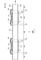
- FIG. 3 is a cross-sectional view illustrating a configuration of the light emitting device 10 according to the first modification, and corresponds to FIG. 1 of the embodiment.
- the light emitting device 10 according to this modification is the same as the light emitting device 10 according to the embodiment, except that the edge of the first optical filter 200 overlaps the region other than the light emitting unit 140 in the first region 102. It is a configuration. In other words, in the present modification, the edge of the first optical filter 200 overlaps the second electrode 130 and the insulating film 150. In other words, the edge of the first optical filter 200 is located between the second region 104 and the light emitting unit 140.
- the peak of the emission spectrum of the light emitting unit 140 can be sharpened and the translucency of the light emitting device 10 can be maintained.
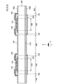
- FIG. 4 is a cross-sectional view illustrating a configuration of a light emitting device 10 according to Modification Example 2, and corresponds to FIG. 1 of the embodiment.
- the light emitting device 10 according to this modification is the same as the light emitting device 10 according to the embodiment, except that the edge of the first optical filter 200 overlaps the region close to the insulating film 150 in the third region 106. It is a configuration.
- the first optical filter 200 covers the light emitting unit 140 and the insulating film 150. Further, the end portion of the first optical filter 200 protrudes into the third region 106.
- the width w1 is preferably 10% or less of the width of the third region 106. In this way, even if a part of the first optical filter 200 protrudes into the third region 106, the transmissivity of the third region 106 (in other words, the translucency of the light emitting device 10) decreases. Can be suppressed.
- the width of the portion located in the third region 106 in one end of the first optical filter 200 is the same as the width of the portion located in the third region 106 in the other end of the first optical filter 200. It may be. May be different.
- the peak of the emission spectrum of the light emitting unit 140 can be sharpened and the translucency of the light emitting device 10 can be maintained.
- the end portion of the first optical filter 200 protrudes into the third region 106, even if the position of the first optical filter 200 with respect to the light emitting unit 140 and the width of the first optical filter 200 vary. It can suppress that the part which is not covered with the 1st optical filter 200 among the light emission parts 140 arises. Of the light from the light emitting unit 140, the light emitted from the second surface 100b without passing through the first optical filter 200 can be reduced.
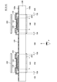
- FIG. 5 is a cross-sectional view illustrating a configuration of a light-emitting device 10 according to Modification 3, and corresponds to FIG. 1 of the embodiment.
- the light emitting device 10 according to this modification has the same configuration as that of the light emitting device 10 according to the embodiment except that the light emitting device 10 includes a sheet member 210.
- the sheet member 210 is formed using, for example, a transparent resin, and is attached to the second surface 100b of the substrate 100 using an adhesive layer or an adhesive layer.
- a first optical filter 200 is formed in a region of the sheet member 210 that faces the light emitting unit 140. However, the first optical filter 200 is not formed in a region of the sheet member 210 that overlaps the third region 106.
- the relative positions of the first optical filter 200 and the first region 102, the second region 104, and the third region 106 are as shown in the embodiment. However, this relative position may be the same as in FIG. 2, the same as in FIG. 3, or the same as in FIG. 4.
- the first optical filter 200 is provided on the surface of the sheet member 210 opposite to the substrate 100.
- the first optical filter 200 may be provided on the surface of the sheet member 210 facing the substrate 100 or may be provided inside the sheet member 210.
- the first optical filter 200 may be formed by coloring a part of the sheet member 210.
- the peak of the emission spectrum of the light emitting unit 140 can be sharpened and the translucency of the light emitting device 10 can be maintained.
- the first optical filter 200 can be attached to the substrate 100 by attaching the sheet member 210 to the substrate 100, the first optical filter 200 can be easily attached to the substrate 100.
- FIG. 6 is a cross-sectional view illustrating a configuration of a light emitting device 10 according to Modification 4.
- the light emitting device 10 according to this modification has the same configuration as that of the light emitting device 10 according to the embodiment except that the second light filter 202 is provided.
- the second optical filter 202 is located on the opposite side of the first optical filter 200 when the light emitting unit 140 is used as a reference.
- the light emitting unit 140 is located between the first optical filter 200 and the second optical filter 202.
- the 2nd optical filter 202 is attached to this sealing member. More specifically, the 2nd optical filter 202 is attached to the surface on the opposite side to the light emission part of this sealing member.
- the sealing member should just be a sealing member which has translucency.
- it may have a so-called hollow sealing structure using a transparent member such as glass, a film such as a laminate film, or a film such as an inorganic film.
- the color of the second optical filter 202 is a complementary color of the color of the first optical filter 200, for example.
- the transmittance of white light in the region where the first optical filter 200 and the second optical filter 202 overlap with each other is 5% or less, preferably approximately 0%.
- the 2nd optical filter 202 may have the characteristic (for example, the characteristic similar to the smoke film for window glass) of not transmitting light more than fixed over the whole region of visible light.
- the transmittance of white light with respect to the second optical filter 202 is, for example, 20% to 70%, but is not limited to this range.
- White light for example, means light corresponding to the light source color of a fluorescent lamp or LED in a range defined as daylight color, daylight white, white, warm white, and light bulb color in JIS, for example.
- Daylight color, daylight white, white, warm white, and light bulb color are as defined in JISZ9112.
- the daylight color is (0.3274, 0.3673), (0.3282, 0.3297), (0.2998, 0.3396), and (0.3064) in the xy chromaticity diagram.
- 0.3091) is a region surrounded by a quadrangle
- the interphase color temperature Tcp is 5700 to 7100 (K).
- lunch white is (0.3616, 0.3875), (0.3552, 0.3476), (0.3326, 0.3635), and (0.3324, 0.3296) in the xy chromaticity diagram.
- White is (0.3985, 0.4102), (0.3849, 0.3668), (0.3652, 0.3880), and (0.3584, 0.3499) in the xy chromaticity diagram.
- the interphase color temperature Tcp is 3800-4500 (K).
- warm white is (0.4305, 0.4218), (0.4141, 0.3834), (0.3966, 0.4044), and (0.3856, 0.3693) in the xy chromaticity diagram.
- the light bulb colors are (0.4834, 0.4832), (0.4594, 0.3971), (0.4305, 0.4218), and (0.4153, 0.3862) in the xy chromaticity diagram.
- the white light may be sunlight.
- the white light is not limited to these examples, and may be, for example, light including light having wavelengths of red (wavelength 640 nm), green (wavelength 520 nm), and blue (wavelength 450 nm).
- white light may be radiation that appears white to the naked eye, usually consisting of a continuous spectrum.
- 90% or more of the second optical filter 202 preferably overlaps the first optical filter 200.
- 90% or more of the first optical filter 200 preferably overlaps with the second optical filter 202.
- the second optical filter 202 is provided to face each of the plurality of first optical filters 200.
- one second optical filter 202 is provided for one first optical filter 200.
- the width of the second optical filter 202 in the direction in which the light emitting units 140 are arranged is, for example, 95% to 105% of the width of the first optical filter 200.
- the width of the second optical filter 202 in the direction in which the light emitting unit 140 extends is, for example, not less than 95% and not more than 105% of the width of the first optical filter 200.
- the width of the second optical filter 202 is not limited to these ranges.
- the 2nd optical filter 202 has the characteristic similar to the smoke film for window glasses as mentioned above (for example, in the case of light brown or black), as shown in FIG.
- One second optical filter 202 may be provided so as to overlap the optical filter 200.
- the second optical filter 202 is also provided in the third region 106 located between the light emitting units 140. Further, the second optical filter 202 may be provided over almost the entire area of the substrate 100.
- the peak of the emission spectrum of the light emitting unit 140 can be sharpened and the translucency of the light emitting device 10 can be maintained.
- the second optical filter 202 is provided at a position overlapping the first optical filter 200, when light other than the light emitting unit 140 passes through the first optical filter 200 at a timing when the light emitting unit 140 does not emit light. It can suppress that at least one part of the light-emitting device 10 seems to have the same color as the 1st optical filter 200.
- the light emitting device 10 may include the second optical filter 202 illustrated in the present modification.
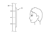
- FIG. 8 is a cross-sectional view for explaining a method of using the light emitting device 10 according to the example.
- the light emitting device 10 is attached to one surface of the translucent member 20.
- the translucent member 20 is, for example, a window glass.
- the light emitting device 10 is a part of the light emitting system.
- the light emitting system includes at least a light emitting device 10 and a light transmitting member 20, and includes a control unit (not shown) that controls the light emitting device 10, a power supply unit (not shown), a fixing member that fixes the light transmitting member 20, and light emission.
- An attachment member for attaching the device 10 to the translucent member 20 is included.
- the translucent member 20 is a window glass of a building or a moving body (for example, an automobile, a train, or an airplane), the light emitting surface (second surface 100b) of the light emitting device 10 faces the translucent member 20, for example. That is, the light emitted from the light emitting device 10 is radiated to the outside of the building or the moving body via the light transmitting member 20.
- the light emission part 140 is provided in the outer surface of a building or a mobile body, the light emission surface of the board
- the light emitting device 10 may be positioned at the same height as the human eye, may be positioned higher than the human eye, or may be positioned lower than the human eye.
- the translucent member 20 may have an inclination.
- the light emitting device 10 has the configuration shown in any of the embodiments and the respective modifications. Therefore, the peak of light emitted from the light emitting device 10 through the light transmitting member 20 can be sharpened. Moreover, the translucency of the area
- the light emission luminance of the light emitting device 10 varies depending on the conditions when it is measured (recognized), for example, the position and angle of the human eye.
- the light emission luminance is maximized in front of the light emitting device 10 (in a direction perpendicular to the light emitting device 10). Therefore, for the light-transmitting member 20 and the light-emitting device 10 having an inclination, it is desired to maximize the light emission luminance at a desired angle, for example, when the light emission of the light-emitting device 10 is maximized when viewed in the horizontal direction.
- the light emitting device 10 may be designed to strengthen a specific wavelength using a resonance structure. In this case, the light emission luminance at a desired angle is improved, but the light emission color of the light emitting device 10 may appear to change when observed from the desired angle and other angles.
- a desired angle for example, the inclination is horizontal with respect to the translucent member 20.
- the light emission at 630 nm is observed at an angle (when viewed from the direction), but the emission color is different at other angles (for example, when viewed from the vertical with respect to the light-transmitting member 20 having an inclination). Due to the resonance structure, light emission at a certain wavelength peak (wavelength near 630 nm) at other angles becomes relatively weak. Therefore, a change in color depending on the observation point of the light emitting device 10 has occurred.
- the color of the light emitting device 10 it can suppress that a taste changes.
Landscapes
- Physics & Mathematics (AREA)
- Optics & Photonics (AREA)
- Engineering & Computer Science (AREA)
- Microelectronics & Electronic Packaging (AREA)
- General Physics & Mathematics (AREA)
- Electroluminescent Light Sources (AREA)
- Optical Filters (AREA)
Abstract
Plusieurs unités électroluminescentes (140) sont agencées sur une première surface (100a) d'un substrat (100), et sont séparées les unes des autres. Les unités électroluminescentes (140) sont pourvues de premières électrodes (110) translucides, d'une couche organique (120) et de secondes électrodes (130) réfléchissant la lumière. La couche organique (120) est positionnée entre les premières électrodes (110) et les secondes électrodes (130). Des zones translucides sont positionnées entre les unités électroluminescentes (140), et transmettent la lumière dans le sens de l'épaisseur de ce dispositif électroluminescent (10). Des filtres optiques (200) chevauchent les unités électroluminescentes (140) et ne chevauchent pas au moins des parties des zones translucides.
Priority Applications (3)
| Application Number | Priority Date | Filing Date | Title |
|---|---|---|---|
| JP2017567008A JPWO2017138632A1 (ja) | 2016-02-12 | 2017-02-10 | 発光装置 |
| US16/077,031 US10454053B2 (en) | 2016-02-12 | 2017-02-10 | Light-emitting device with a first and a second optical filter |
| US16/569,314 US10686151B2 (en) | 2016-02-12 | 2019-09-12 | Light-emitting device with see-through property using optical filters |
Applications Claiming Priority (2)
| Application Number | Priority Date | Filing Date | Title |
|---|---|---|---|
| JP2016-025292 | 2016-02-12 | ||
| JP2016025292 | 2016-02-12 |
Related Child Applications (2)
| Application Number | Title | Priority Date | Filing Date |
|---|---|---|---|
| US16/077,031 A-371-Of-International US10454053B2 (en) | 2016-02-12 | 2017-02-10 | Light-emitting device with a first and a second optical filter |
| US16/569,314 Continuation US10686151B2 (en) | 2016-02-12 | 2019-09-12 | Light-emitting device with see-through property using optical filters |
Publications (1)
| Publication Number | Publication Date |
|---|---|
| WO2017138632A1 true WO2017138632A1 (fr) | 2017-08-17 |
Family
ID=59563480
Family Applications (1)
| Application Number | Title | Priority Date | Filing Date |
|---|---|---|---|
| PCT/JP2017/004915 Ceased WO2017138632A1 (fr) | 2016-02-12 | 2017-02-10 | Dispositif électroluminescent |
Country Status (3)
| Country | Link |
|---|---|
| US (2) | US10454053B2 (fr) |
| JP (4) | JPWO2017138632A1 (fr) |
| WO (1) | WO2017138632A1 (fr) |
Families Citing this family (3)
| Publication number | Priority date | Publication date | Assignee | Title |
|---|---|---|---|---|
| CN111584754B (zh) * | 2020-05-27 | 2022-07-12 | 京东方科技集团股份有限公司 | 显示面板及其制备方法、显示装置 |
| US20220045133A1 (en) * | 2020-08-05 | 2022-02-10 | Joled Inc. | Display panel and display device |
| KR102902751B1 (ko) * | 2021-12-28 | 2025-12-19 | 엘지디스플레이 주식회사 | 투명 표시 장치 |
Citations (7)
| Publication number | Priority date | Publication date | Assignee | Title |
|---|---|---|---|---|
| JP2006054200A (ja) * | 2005-10-28 | 2006-02-23 | Casio Comput Co Ltd | El素子 |
| JP2007115626A (ja) * | 2005-10-24 | 2007-05-10 | Seiko Epson Corp | 有機el装置 |
| JP2011129392A (ja) * | 2009-12-18 | 2011-06-30 | Seiko Epson Corp | 表示装置 |
| US20110220901A1 (en) * | 2010-03-09 | 2011-09-15 | Jae-Heung Ha | Organic light-emitting display device |
| JP2011228249A (ja) * | 2010-03-29 | 2011-11-10 | Tdk Corp | 透過型カラー有機el表示装置 |
| JP2012234798A (ja) * | 2011-05-03 | 2012-11-29 | Samsung Mobile Display Co Ltd | 有機発光表示装置 |
| JP2013117719A (ja) * | 2011-11-04 | 2013-06-13 | Semiconductor Energy Lab Co Ltd | 表示装置、及びその駆動方法 |
Family Cites Families (7)
| Publication number | Priority date | Publication date | Assignee | Title |
|---|---|---|---|---|
| JP2004206076A (ja) * | 2002-12-10 | 2004-07-22 | Pioneer Electronic Corp | フラットディスプレイ装置 |
| WO2007148411A1 (fr) * | 2006-06-22 | 2007-12-27 | Pioneer Corporation | Dispositif d'affichage |
| JP4816985B2 (ja) | 2009-06-16 | 2011-11-16 | Tdk株式会社 | 有機el表示装置 |
| JP6157866B2 (ja) | 2013-02-04 | 2017-07-05 | 株式会社東芝 | 有機電界発光素子、照明装置及び照明システム |
| JP5584329B1 (ja) * | 2013-02-04 | 2014-09-03 | 株式会社東芝 | 有機電界発光素子、照明装置及び照明システム |
| WO2015079519A1 (fr) * | 2013-11-27 | 2015-06-04 | 株式会社 東芝 | Élément électroluminescent organique, appareil d'éclairage et système d'éclairage |
| JPWO2017138633A1 (ja) * | 2016-02-12 | 2018-11-29 | パイオニア株式会社 | 発光装置 |
-
2017
- 2017-02-10 WO PCT/JP2017/004915 patent/WO2017138632A1/fr not_active Ceased
- 2017-02-10 US US16/077,031 patent/US10454053B2/en active Active
- 2017-02-10 JP JP2017567008A patent/JPWO2017138632A1/ja active Pending
-
2019
- 2019-09-12 US US16/569,314 patent/US10686151B2/en active Active
-
2020
- 2020-09-15 JP JP2020154734A patent/JP2021007101A/ja active Pending
-
2022
- 2022-03-31 JP JP2022058313A patent/JP2022079636A/ja active Pending
-
2023
- 2023-12-01 JP JP2023203644A patent/JP2024020601A/ja not_active Withdrawn
Patent Citations (7)
| Publication number | Priority date | Publication date | Assignee | Title |
|---|---|---|---|---|
| JP2007115626A (ja) * | 2005-10-24 | 2007-05-10 | Seiko Epson Corp | 有機el装置 |
| JP2006054200A (ja) * | 2005-10-28 | 2006-02-23 | Casio Comput Co Ltd | El素子 |
| JP2011129392A (ja) * | 2009-12-18 | 2011-06-30 | Seiko Epson Corp | 表示装置 |
| US20110220901A1 (en) * | 2010-03-09 | 2011-09-15 | Jae-Heung Ha | Organic light-emitting display device |
| JP2011228249A (ja) * | 2010-03-29 | 2011-11-10 | Tdk Corp | 透過型カラー有機el表示装置 |
| JP2012234798A (ja) * | 2011-05-03 | 2012-11-29 | Samsung Mobile Display Co Ltd | 有機発光表示装置 |
| JP2013117719A (ja) * | 2011-11-04 | 2013-06-13 | Semiconductor Energy Lab Co Ltd | 表示装置、及びその駆動方法 |
Also Published As
| Publication number | Publication date |
|---|---|
| US20200006691A1 (en) | 2020-01-02 |
| JP2022079636A (ja) | 2022-05-26 |
| JP2024020601A (ja) | 2024-02-14 |
| JP2021007101A (ja) | 2021-01-21 |
| US10454053B2 (en) | 2019-10-22 |
| JPWO2017138632A1 (ja) | 2018-11-29 |
| US20190036057A1 (en) | 2019-01-31 |
| US10686151B2 (en) | 2020-06-16 |
Similar Documents
| Publication | Publication Date | Title |
|---|---|---|
| JP2024020601A (ja) | 発光装置 | |
| CN110518151A (zh) | 显示面板及显示装置 | |
| WO2016042638A1 (fr) | Dispositif électroluminescent | |
| JP2024015135A (ja) | 発光装置 | |
| US9231229B2 (en) | Light emitting panel and manufacturing method of light emitting panel | |
| JP5846345B1 (ja) | 面状発光ユニット | |
| JP2016062767A (ja) | 発光装置 | |
| JPWO2015079912A1 (ja) | 面状発光ユニット | |
| JP6754826B2 (ja) | 発光装置 | |
| JP2017103048A (ja) | 発光装置及び発光システム | |
| WO2017073459A1 (fr) | Système électroluminescent | |
| US20200028118A1 (en) | Light-emitting system | |
| JP5540727B2 (ja) | 発光装置 | |
| JP6947514B2 (ja) | 発光システム | |
| JP2018137093A (ja) | 発光装置 | |
| JP2017103049A (ja) | 発光装置及び発光システム | |
| JP2014157759A (ja) | 有機エレクトロルミネッセンスパネル及び、有機elパネル複合体 | |
| JP2016195081A (ja) | 面発光モジュール | |
| JP2016096029A (ja) | 発光素子、およびこれを有する窓 | |
| WO2017094499A1 (fr) | Dispositif électroluminescent | |
| JP2017084517A (ja) | 面発光モジュール |
Legal Events
| Date | Code | Title | Description |
|---|---|---|---|
| 121 | Ep: the epo has been informed by wipo that ep was designated in this application |
Ref document number: 17750353 Country of ref document: EP Kind code of ref document: A1 |
|
| WWE | Wipo information: entry into national phase |
Ref document number: 2017567008 Country of ref document: JP |
|
| NENP | Non-entry into the national phase |
Ref country code: DE |
|
| 122 | Ep: pct application non-entry in european phase |
Ref document number: 17750353 Country of ref document: EP Kind code of ref document: A1 |