WO2017141539A1 - Dispositif de commande d'onduleur - Google Patents
Dispositif de commande d'onduleur Download PDFInfo
- Publication number
- WO2017141539A1 WO2017141539A1 PCT/JP2016/087867 JP2016087867W WO2017141539A1 WO 2017141539 A1 WO2017141539 A1 WO 2017141539A1 JP 2016087867 W JP2016087867 W JP 2016087867W WO 2017141539 A1 WO2017141539 A1 WO 2017141539A1
- Authority
- WO
- WIPO (PCT)
- Prior art keywords
- voltage vector
- current
- unit
- phase
- current value
- Prior art date
- Legal status (The legal status is an assumption and is not a legal conclusion. Google has not performed a legal analysis and makes no representation as to the accuracy of the status listed.)
- Ceased
Links
Images





Classifications
-
- H—ELECTRICITY
- H02—GENERATION; CONVERSION OR DISTRIBUTION OF ELECTRIC POWER
- H02M—APPARATUS FOR CONVERSION BETWEEN AC AND AC, BETWEEN AC AND DC, OR BETWEEN DC AND DC, AND FOR USE WITH MAINS OR SIMILAR POWER SUPPLY SYSTEMS; CONVERSION OF DC OR AC INPUT POWER INTO SURGE OUTPUT POWER; CONTROL OR REGULATION THEREOF
- H02M7/00—Conversion of AC power input into DC power output; Conversion of DC power input into AC power output
- H02M7/42—Conversion of DC power input into AC power output without possibility of reversal
- H02M7/44—Conversion of DC power input into AC power output without possibility of reversal by static converters
- H02M7/48—Conversion of DC power input into AC power output without possibility of reversal by static converters using discharge tubes with control electrode or semiconductor devices with control electrode
-
- H—ELECTRICITY
- H02—GENERATION; CONVERSION OR DISTRIBUTION OF ELECTRIC POWER
- H02P—CONTROL OR REGULATION OF ELECTRIC MOTORS, ELECTRIC GENERATORS OR DYNAMO-ELECTRIC CONVERTERS; CONTROLLING TRANSFORMERS, REACTORS OR CHOKE COILS
- H02P27/00—Arrangements or methods for the control of AC motors characterised by the kind of supply voltage
- H02P27/04—Arrangements or methods for the control of AC motors characterised by the kind of supply voltage using variable-frequency supply voltage, e.g. inverter or converter supply voltage
- H02P27/06—Arrangements or methods for the control of AC motors characterised by the kind of supply voltage using variable-frequency supply voltage, e.g. inverter or converter supply voltage using DC to AC converters or inverters
Definitions
- the present invention relates to an inverter control device for controlling an inverter that converts DC power used in a rotating machine, in particular, an electric motor into AC power.
- a voltage command vector that creates a voltage command vector that is a vector of voltages that should be followed by the three-phase voltage of the inverter and that is a composite voltage vector of the three-phase voltages of each phase.
- a voltage command vector correction unit that corrects the generated voltage command vector, and controls the inverter according to the corrected voltage command vector, and the voltage command vector correction unit includes the voltage command vector correction unit.
- the voltage command vector after being corrected by the correcting means is corrected so as to be a vector outside the region where the three-phase current cannot be detected in the current detection interval, and in the current non-detection interval within the carrier period, It is disclosed that reverse correction is performed to cancel the correction in the current detection section.
- two basic voltage vector components V4 and V5 having different phases of 60 degrees capable of generating a command voltage vector are output within a first period of 1 PWM cycle.
- two basic voltage vector components V1 and V2 that are 180 degrees out of phase with respect to the basic voltage vector component are output within a second period that forms one PWM cycle continuous with the first period. Therefore, even when the degree of modulation is small or when the phase of the output voltage vector is close to a single basic voltage vector, the pulse width is sufficiently long, and current detection can be performed with high accuracy. This makes it possible to detect current with high accuracy even when the degree of modulation is small or when the phase of a single basic voltage vector is close.
- JP 2012-178927 A Japanese Patent Laid-Open No. 2005-12934
- the three-phase alternating current can be restored only once every two switching cycles, and the current detection accuracy is lowered when the carrier frequency is small and the switching cycle is long. there were.
- the present invention has been made to solve the above-described problem, and restores a three-phase AC current value based on a current value for two phases detected from a DC bus without depending on a three-phase voltage command.
- An object of the present invention is to provide an inverter control device capable of reducing the beat sound.
- an inverter control device includes an inverter control unit that controls a switching element of an inverter that converts DC power into AC power according to a predetermined switching time, and a DC that supplies DC power to the inverter.
- a current detection unit that detects a current value of a power supply; a detection current storage unit that sets a current value detection time based on the switching time; and acquires, stores, and holds the current value from the current detection unit; and the detection Based on the phase current calculation unit that calculates and restores the AC current value generated by the inverter from the current values for the number of phases required for restoration from the current storage unit, and based on the restored AC current value and the rotational speed command value
- a command voltage vector generator for generating a command voltage vector, and a command voltage vector corrected based on the command voltage vector.
- a correction command voltage vector generation unit to be configured, and a switching time setting unit that sets the switching time based on the corrected command voltage vector and outputs the switching time to the inverter control unit and the detected current storage unit
- the correction command voltage vector generator generates a vector when n is 3 or more in n periods (n is a natural number of 2 or more) of the unit period, where 1 ⁇ 2 of the switching period of the inverter is a unit period. Apply a plurality of voltage vectors whose total is a zero vector, and when n is 2, apply a plurality of voltage vectors whose total is a zero vector in the four periods of the unit period to correct the correction
- the command voltage vector thus generated is generated.
- the inverter control apparatus of the present invention in the n period where 1 ⁇ 2 of the switching period is a unit period and n is a natural number of 3 or more, the total of the voltage vectors for detection becomes a zero vector in at least two periods.
- the current value detection section for applying the voltage vector based on the command voltage vector is set, so detection is performed in each control cycle without depending on the command voltage vector. It is possible to set the phase, whereby the magnitude of the current pulsation changes periodically by setting k to a natural number of n or less and the voltage vector to be applied to the kth in the n period always being the same. In particular, there is an effect that it is possible to reduce the roaring sound that is derived from the noise.
- FIG. 1 is a schematic configuration diagram of a motor control system including an inverter control device according to Embodiment 1.
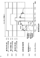
- FIG. FIG. 10 is a diagram for describing a procedure for setting a current detection time for acquiring a current value from a DC bus by the current detection unit in the first embodiment.
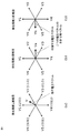
- 6 is a diagram illustrating an example of a voltage vector applied in a correction command voltage vector generation unit in the first embodiment.
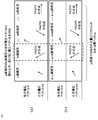
- FIG. 6 is a diagram illustrating an example of a voltage vector applied in each cycle in the first embodiment.
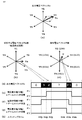
- FIG. 6 is a diagram illustrating an example of switching of a voltage vector to be applied in Embodiment 1.
- FIG. It is a figure explaining the relationship between the command voltage vector in Embodiment 1, the applied voltage vector, and switching time.
- FIG. 10 is a diagram for describing a procedure for setting a current detection time for acquiring a current value from a DC bus by the current detection unit in the first embodiment.
- 6 is a diagram illustrating an example of a voltage vector
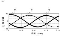
- FIG. 4 is a diagram showing an output current waveform of an inverter in the first embodiment. It is a figure which shows the output current waveform of the inverter of a prior art.
- FIG. 3 is a diagram illustrating a hardware configuration of the inverter control device according to the first embodiment. It is a schematic block diagram of the motor control system containing the inverter control apparatus which concerns on Embodiment 2. It is a figure explaining the relationship between the command voltage vector in Embodiment 2, the voltage vector to apply, and switching time.
- FIG. 1 is a schematic configuration diagram of a motor control system including an inverter control device according to the first embodiment.
- FIG. 2 is a diagram for explaining a procedure for setting a current value detection time for acquiring a current value from a DC bus by the current detection unit.
- FIG. 3 is a diagram illustrating an example of a voltage vector applied in the correction command voltage vector generation unit.
- FIG. 4 is a diagram for explaining an example of a voltage vector applied in each cycle.
- FIG. 5 is a diagram illustrating an example of switching of a voltage vector to be applied.
- FIG. 6 is a diagram for explaining the relationship between the command voltage vector, the applied voltage vector, and the switching time.
- FIG. 7 is a diagram illustrating an output current waveform of the inverter.
- the motor control system 1 includes a motor 2 that is a rotating machine, an inverter 3 that supplies a three-phase AC current value to the motor 2, and DC power that is supplied to the inverter 3.
- a DC power supply 4, a DC bus 5 that energizes and connects the DC power supply 4 and the inverter 3, and an inverter control device 10 that controls the inverter 3 are configured.
- the inverter 3 includes three pairs (for three phases) of a pair of switching elements 31s on the upper arm 31 (positive side) and switching elements 32s on the lower arm 32 (negative side), and switching elements 31s for these phases. , 32s and diodes 31d, 32d connected in antiparallel to each other, and the inverter control device 10 controls conduction / shutoff (on / off) of the switching elements 31s, 32s of each phase.
- the DC power supplied from the DC power supply 4 is converted into three-phase AC power.
- the electric motor 2 as a load is driven by the three-phase AC power.
- a semiconductor switching element such as a MOSFET (Metal-Oxide-Semiconductor Field-Effect Transistor) is generally used.
- the inverter control device 10 acquires a current value Idc from the current detection unit 11 at a set current value detection time, and a current detection unit 11 that detects a current value flowing through the DC bus 5.
- the detection current storage unit 12 for storing and holding, and the three-phase AC current values Iu, Iv, Iw flowing in the motor 2 from the two-phase current values IdcA, IdcB stored in the detection current storage unit 12 are restored.
- the command voltage vector generation unit 14 that generates the command voltage, and the three-phase command voltage vectors Vu, Vv, and Vw generated by the command voltage vector generation unit 14 are compared with the current three-phase command voltage vectors Vu, Vv, and Vw.
- the corrected command voltage vector generation unit 15 for generating the corrected three-phase command voltage vectors Vu ′, Vv ′, Vw ′, and the three-phase command voltage vector Vu ′ corrected by the correction command voltage vector generation unit 15 , Vv ′, Vw ′, a switching time setting unit 16 for setting a switching time for driving the switching elements 31 s, 32 s, and a switching time Sup, Svp, Swp, Swn, Svn, set by the switching time setting unit 16 Sun outputs on / off control signals Guu, Gvu, Gwu to the gates of the three-phase switching elements 31s, 32s, and outputs on / off control signals Gul, Gvl, Gwl to the gates of the three-phase switching elements 32s, respectively.
- an inverter control unit 17 for generating the corrected three-phase command voltage vectors Vu ′, Vv ′, Vw ′, and the three-phase command voltage vector Vu ′ corrected by the correction command voltage vector generation unit 15 ,
- the current detection unit 11 includes a current detection element for detecting a current value installed in the path of the DC bus 5.
- a current detection element for example, a Hall sensor, a resistor, a current transformer, or the like is used to detect the voltage across the current detection element or the output voltage via an amplifier and a buffer as necessary.
- the current detection element is provided on the low voltage (negative electrode) side of the DC power supply 4
- the case where the current detection element is provided on the high voltage (positive electrode) side may be used. It does not affect the operation of the present embodiment.
- the detection current storage unit 12 acquires and stores the current value Idc from the current detection unit 11 at current value detection times Ta and Tb set by the switching time setting unit 16 described later.
- the detected current values IdcA and IdcB for two phases are held.
- the phase current calculation unit 13 uses the current values IdcA and IdcB for two phases detected from the DC bus 5 stored in the detection current storage unit 12, and the three-phase AC current value flowing in the motor 2. Iu, Iv, Iw are calculated and restored. Here, the three-phase AC current values Iu, Iv are corrected using the corrected three-phase command voltage vectors Vu ′, Vv ′, Vw ′ output from the correction command voltage vector generation unit 15 described later. , Iw is calculated.
- the command voltage vector generation unit 14 is set for each set switching cycle based on the rotation speed command value Wref according to an instruction from the outside and the three-phase AC current values Iu, Iv, Iw restored by the phase current calculation unit 13. Then, new three-phase command voltage vectors Vu, Vv, and Vw, which are driving targets of the inverter 3, are generated and updated.
- the corrected command voltage vector generation unit 15 has a current for two phases having a magnitude that enables current value detection with respect to the three-phase command voltage vectors Vu, Vv, and Vw generated by the command voltage vector generation unit 14.
- a voltage vector Va for value detection and a voltage vector Vb for canceling the voltage vector Va are applied to generate corrected three-phase command voltage vectors Vu ′, Vv ′, Vw ′, and a switching time setting unit 16 Output to.
- the newly corrected three-phase command voltage vectors Vu ′, Vv ′, and Vw ′ are also output to the phase current calculation unit 13 and used.
- the switching time setting unit 16 switches the switching elements 31 s, 32 s constituting the inverter 3.
- the switching times Sup, Svp, Swp, Swn, Svn, Sun to be driven are set, and the switching elements 31s, 32s are turned on / off at the set switching times Sup, Svp, Swp, Swn, Svn, Sun.
- the inverter 3 is driven by outputting a control signal.
- the detection current storage unit 12 sets the current value detection times Ta and Tb using the switching times Sup, Svp, Swp, Swn, Svn, Sun set by the switching time setting unit 16, and the set current value detection At times Ta and Tb, the current values IdcA and IdcB of the DC bus 5 detected by the current detector 11 are acquired, stored and held.
- the inverter control unit 17 uses the switching times Sup, Svp, Swp, Swn, Svn, Sun set by the switching time setting unit 16 and supplies an on / off control signal to the gate of the switching element 31s of the upper arm. Guu, Gvu, Gwu are output. At the same time, on / off control signals Gul, Gvl, Gwl opposite to those of the upper arm switching element 31s are output to the gate of the lower arm switching element 32s.
- FIG. 2 is a diagram for explaining a procedure for setting the current value detection times Ta and Tb from the switching times Sup, Svp, and Swp of the switching element 31 s constituting the upper arm.
- FIG. 2 (a), FIG. 2 (b), and FIG. 2 (c) show the switch states of the switching element 31s constituting the upper arm of each phase, and each of the voltage maximum phase (U phase). The switch state, the voltage intermediate phase (V phase) switch state, and the voltage minimum phase (W phase) switch state are shown.
- 2 (d) shows the current value of the DC bus 5
- FIG. 2 (e) shows the current value detection times Ta and Tb
- FIG. 2 (f) shows the switching times Sup, Svp, Swp, Swn, Svn, Sun are shown.
- the switching time setting unit 16 sets the current value detection times Ta and Tb using the switching times Sup, Svp, and Swp of the switching element 31s.
- the switch states of the three-phase upper arm switching elements 31 s are all on or not all off, that is, non-zero vector switches It is necessary to select two types from the current value detection section, which is a state section, and perform detection in that section. Therefore, the current value detection times Ta and Tb for detecting the current values IdcA and IdcB are set depending on the switching time of the voltage intermediate phase (V phase) switching element 31s.
- the largest voltage phase, the middle voltage phase, and the smallest voltage phase are defined in order from the largest.
- FIG. 2 shows a case where Vu ′ is the maximum voltage phase (U phase), Vv ′ is the voltage intermediate phase (V phase), and Vw ′ is the minimum voltage phase (W phase).
- FIGS 2A, 2B, and 2C show the switch state of the switching element 31s that constitutes the upper arm of each phase, the switching element that constitutes the lower arm.
- the 32s switch state is the opposite of the upper switch state. That is, when the switching element 31s of the upper arm of the maximum voltage phase (U phase) is on (conducting), the switching element 32s of the lower arm of the maximum voltage phase (U phase) is turned off (cut off).
- the current value of the DC bus 5 detected during the first non-zero voltage vector period is detected as IdcA, and the second non-zero voltage vector period is detected.
- the current value of the DC bus 5 is IdcB. 2 which is the current value detection time of the current value IdcA is set a predetermined time T1 before the switching time Svp of the voltage intermediate phase (V phase) switching element 31s.
- T1 is set to a time longer than the time required for current value detection.
- Tb in FIG. 2 which is the current value detection time of the current value IdcB is set after a predetermined time T2 from Ta.
- T2 considers a dead time interval provided in order to prevent the switching elements 31s and 32s pair connected in series in the inverter 3 from being conducted simultaneously, and the current value Idc of the DC bus 5 is In some cases, the current vibrates due to a sudden change in voltage associated with the on / off operation of the switching elements 31s and 32s, and it is necessary to set the current in consideration of the vibration of the current.
- FIG. 2 shows an example of this, and the current oscillates due to a sudden change in voltage accompanying the on / off operation of the switching element 31s in the non-zero voltage vector section of the switching times Sup, Svp, Swp of the switching element 31s.
- a section in which value detection is impossible hereinafter referred to as a current value non-detectable section Ti
- a current value detectable section Tp are described. Therefore, T2 is set so that Tb does not enter the current value non-detectable section Ti.
- IdcA indicates the current value of the maximum voltage phase (U phase)
- IdcB indicates the current value of the minimum voltage phase (W phase).
- the phase current calculation unit 13 calculates the current value of the voltage intermediate phase (V phase) from the current values of the two phases, and the difference between the current value detection times of IdcA and IdcB is set as short as possible. This is because current flows through the electric motor 2 due to the non-zero voltage vector and the current value of the DC bus 5 also changes. Therefore, if Ta and Tb are separated, the current value detection accuracy of the voltage intermediate phase (V phase) decreases. It is to do.
- FIG. 2 shows an example in which current value detection is performed in the first two non-zero voltage vector periods of four non-zero voltage vector periods in the switching period T.
- the current value may be detected in the vector period, and the same processing is performed.
- IdcA indicates the current value of the DC bus 5 detected during the third non-zero voltage vector period
- IdcB indicates the current value of the DC bus 5 detected during the fourth non-zero voltage vector period. Will be shown.
- IdcA indicates the current value of the minimum voltage phase (W phase)
- IdcB indicates the current value of the maximum voltage phase (U phase).
- the phase current calculation unit 13 has a role of restoring the three-phase AC current values Iu, Iv, and Iw from the detected current values IdcA and IdcB for two phases stored in the detected current storage unit 12. Based on the three-phase command voltage vectors Vu, Vv, and Vw generated by the command voltage vector generation unit 14, the signs of the two-phase current values are determined. The remaining one-phase current value can be easily obtained from the two-phase current values IdcA and IdcB whose signs have already been determined by utilizing the fact that the sum of the three-phase current values is zero. By the above calculation, it is possible to restore the three-phase AC current values Iu, Iv, and Iw that flow through the electric motor 2 that is required.
- the calculated three-phase AC current values Iu, Iv, and Iw are used for, for example, update (generation) processing of the three-phase command voltage vector in the command voltage vector generation unit 14 or used for output monitoring of the electric motor 2. It is used for control processing of each part.
- the command voltage vector generation unit 14 has a role of generating target three-phase command voltage vectors Vu, Vv, and Vw output from the inverter 3.
- Various command voltage vector generation methods are known depending on the control method of the electric motor 2, but are not the essence of the present invention.
- the correction command voltage vector generation unit 15 has a role of applying a voltage vector to the command voltage vector V (Vu, Vv, Vw) generated by the command voltage vector generation unit 14.
- the applied voltage vector is a voltage vector that makes it possible to secure a current value detection section for two phases.
- the voltage vectors are different voltage vectors Va and Vb, respectively. It is necessary to satisfy the condition that the sum of the voltage vectors Va and Vb applied at a unit cycle of n is a zero vector, with 1/2 being a unit cycle.
- the voltage vectors Va and Vb applied in each cycle of the switching cycle are preferably combined vectors of continuous basic voltage vectors V1 (100) to V6 (101) in order to reduce switching loss.
- the three numbers in parentheses of the basic voltage vector represent the switch states of the U-phase, V-phase, and W-phase switching elements 31s from the left in the case of the upper-arm switching element 31s, and “1 "" Represents on and "0" represents off.
- V1 (100) indicates that the U-phase switching element 31s is on and the other-phase switching elements 31s are off. The same applies to the lower arm switching element 32s.
- the unit period n is assumed to be 3 for the sake of simplicity.
- V1 (100) and V2 (110) are output based on the command voltage vector V
- V2 (110) and V3 (010) are output as the voltage vector Va for securing the current value detection section.
- V5 (001) so that the voltage vector Va in the second period of the unit period is canceled as the voltage vector Vb for securing the current value detection section.
- V6 (101) is output.
- the command voltage vector V is equal to the command voltage vector V before application of the voltage vectors Va and Vb when viewed as a total of three unit cycles.
- FIG. 4 shows an example of the relationship between the command voltage vector V and the output voltage vector Vo in each unit cycle.
- 4A shows the relationship between the command voltage vector V and the output voltage vector Vo from the first cycle to the nth cycle when the unit cycle is n
- FIG. 4B shows the n + n cycle from the (n + 1) th cycle.
- the relationship between the command voltage vector V up to the eye and the output voltage vector Vo is shown.
- a voltage vector obtained by combining V6 and V1 is applied to the k cycle
- a voltage vector obtained by combining V4 and V5 is applied to the m cycle
- V2 is applied to the n cycle.
- the sum of the voltage vectors applied during the unit period from the first period to the n-th period is a zero vector, so the output voltage vector Vo in the first period is the same as the command voltage vector V. It becomes.
- a voltage vector obtained by combining V6 and V1 is applied to the kth cycle, and a voltage vector obtained by combining V4 and V5 is applied to the mth cycle, A voltage vector obtained by combining V2 and V3 is applied in the nth period.
- the (n + 1) -th cycle output voltage vector Vo is the same as the command voltage vector V.
- the values of the output voltage vector Vo in the first period and the output voltage vector Vo in the n + 1 period are different. That is, the sum of the voltage vectors applied during the unit period is a zero vector, and the same voltage vector is always applied in the kth period and the n + kth period every n periods. That is, a voltage vector that does not depend on the command voltage vector V is applied.
- FIG. 5 shows an example of switching the applied voltage vector.
- the voltage vector applied to the k period of the n period (the voltage vector obtained by combining V6 and V1) always applies the same voltage vector, but a period larger than the drive period, for example, an inverter A voltage vector (a voltage vector obtained by synthesizing V4 and V5) different from that before the operation stop is applied at such a timing that 3 stops the operation and then restarts.
- the switched voltage vector always applies the same voltage vector every n cycles.
- the correction command voltage vector generation unit 15 has a current for two phases having a magnitude that allows current value detection with respect to the three-phase command voltage vector V generated by the command voltage vector generation unit 14.
- a voltage vector Va for value detection and a voltage vector Vb for canceling the voltage vector Va are applied to generate corrected three-phase command voltage vectors Vu ′, Vv ′, Vw ′.
- the switching time setting unit 16 switches the switching times Sup, Svp, Swp, Sun, Svn based on the corrected three-phase command voltage vectors Vu ′, Vv ′, Vw ′ generated by the correction command voltage vector generation unit 15. , Swn is set.
- FIG. 6 is a diagram for explaining the relationship between the command voltage vector, the applied voltage vector, and the switching time.
- FIG. 6 shows an example when the switching times Sup to Swn are set based on the command voltage vector V in the first cycle generated in FIG. 6A shows the output voltage vector Vo
- FIG. 6B shows the voltage vector Va to be applied
- FIG. 6C shows the command voltage vector V
- FIG. , The output voltage vector Vo is shown.
- FIG. 6 (e) FIG.
- FIG. 6 (f), and FIG. 6 (g) show the switch state of the gate of the switching element 31s of the upper arm of each phase, The switch state of the phase (U phase), the switch state of the voltage intermediate phase (V phase), and the switch state of the minimum voltage phase (W phase) are shown.
- the switch state of the gate of the switching element 32s of the lower arm is opposite to the switch state of the gate of the switching element 31s of the upper arm.
- FIG. 6H shows the switching times Sup, Svp, Swp, Swn, Svn, Sun of the switching elements 31s, 32s.
- the command voltage vector V (FIG. 6 (c)) and the applied voltage vector Va (FIG. 6 (b)) are output separately within n periods of the unit period. Is done.
- the numbers in parentheses in the output voltage vector Vo column indicate basic voltage vectors. “0” represents V0 (000), all three-phase switching elements 31s are in an off state, “7” represents V7 (111), and all three-phase switching elements 31s are in an on state. It shows that each. In the example of FIG.
- the V-phase switching element 31 s is turned on based on the applied voltage vector Va, and the U-phase switching element 31 s is turned on. Subsequently to the state, all of the three-phase switching elements 31s are turned on. Further, based on the command voltage vector V, the W-phase switching elements 31s are turned off, and the V-phase and W-phase switching elements 31s. Is finally turned off, and finally all the three-phase switching elements 31s are turned off.
- the section of the output pulsed voltage for switching becomes the current value detection section of the DC bus 5.
- the command voltage vector V and the applied voltage vector Va are output separately within the switching period, the current value can be detected in the output section of the applied voltage vector Va in each switching period.
- the three-phase AC current values Iu, Iv, and Iw can be restored.
- the inverter control unit 17 performs on / off control on the gate of the three-phase switching element 31s of the upper arm based on the switching times Sup, Svp, Swp, Sun, Svn, Swn set by the switching time setting unit 16.
- the signals Guu, Gvu, and Gwu are supplied to the gate of the three-phase switching element 32s of the lower arm, and the on / off control signal Gul, inverted from the three-phase switching element 31s of the upper arm.
- Gvl and Gwl are output, and the phase current output by the inverter 3 is controlled.
- FIG. 7 shows an example of the output waveform of the phase current by the inverter control device of the present embodiment.
- the output waveform of the phase current by the conventional inverter control method shown by patent document 1 is shown in FIG.
- the waveform of the phase current in the case of driving at a switching frequency of 2 kHz and a frequency command of 0.5 Hz is shown.
- the periodic current ripple change portion surrounded by a circle in FIG. 8 generated in the prior art is reduced in the present embodiment.
- the current value detection interval is set by applying a voltage vector based on the command voltage vector.
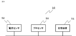
- FIG. 9 shows the hardware configuration of the inverter control device according to the first embodiment.
- the inverter control device 10 is composed of a processor 50, a storage device 51, and a current sensor 52. These are realized.
- the storage device 51 stores various data such as data obtained by calculation, a detected current value, and a three-phase command voltage vector.
- the processor 50 performs an operation using each program and data necessary for executing the operation of the present embodiment stored in the storage device 51.
- the current sensor 52 that is a current detection element acquires a current value from the DC bus 5.
- the storage device 51 includes a volatile storage device such as a random access memory and a nonvolatile auxiliary storage device such as a flash memory. Further, as the nonvolatile auxiliary storage device, an auxiliary storage device such as a hard disk may be provided instead of the flash memory.
- FIG. FIG. 10 is a schematic configuration diagram of a motor control system including the inverter control device according to the second embodiment.
- FIG. 11 is a diagram for explaining the relationship between the command voltage vector, the applied voltage vector, and the switching time.
- the difference between the inverter control device according to the second embodiment and the inverter control device according to the first embodiment is that the inverter control device 20 in the motor control system 9 according to the second embodiment stores the detected current as shown in FIG.
- the part 12 is changed to a detected current storage part 22, and the phase current calculation part 13 is changed to a phase current calculation part 23.
- the other components are the same as those in FIG.
- the command voltage vector V and the voltage vector Va to be applied for securing a current value detection section are separately set for each cycle of a unit cycle that is 1 ⁇ 2 of the switching cycle.
- the output voltage vector Vo needs to be the same as the command voltage vector V in unit period n. Therefore, at least two unit cycles are required to apply the applied voltage vectors Va and Vb, and when combined with at least one unit cycle for outputting the command voltage vector V, three unit cycles are required.
- the second embodiment as shown in FIG.
- the switching time setting unit 16 sets the command voltage vector V to one of the two periods of the unit cycle and the voltage vector Va applied to secure the current value detection section to the other. Output. Further, the order in which the separate output of the command voltage vector V and the applied voltage vectors Va and Vb is output every switching cycle is changed. Along with this, the position of the current value detection is also switched every cycle. In this way, it is possible to cancel the voltage vector Va applied for current value detection applied in the first cycle with the voltage vector Vb applied for current value detection applied in the second cycle. The voltage vector Vb to be applied for cancellation as shown in FIG. It becomes possible.
- the detected current storage unit 22 has a function of acquiring and storing the detected current values IdcA, IdcB, IdcC, and IdcD for the two most recent switching cycles.
- the phase current calculation unit 23 detects the four detected values.
- a function of calculating three-phase AC current values Iu1, Iv1, Iw1, Iu2, Iv2, Iw2 for two switching cycles from the current value and outputting the averaged three-phase AC current values Iu, Iv, Iw have.
- one of the two unit cycles is output as a command voltage vector, and the other is output as a voltage vector applied to secure a current value detection section. Since the value detection section is set, it is possible to set the phase to be detected in each control cycle without depending on the command voltage vector, and thereby the voltage vector to be applied first in the two cycles. Is always the same, there is an effect that it is possible to further reduce the roaring sound that is a noise derived from the periodic change in the magnitude of the current pulsation.
- the inverter control device is useful for motor control systems that are widely compatible with systems that drive rotating machines such as various electric motors, and is particularly driven in a region where a low triangular carrier frequency and a command voltage modulation rate are low. Suitable for motor control system that performs
- the present invention can be freely combined with each other, or can be appropriately modified or omitted.
- 1,9 motor control system 2 electric motor, 3 inverter, 4 DC power supply, 5 DC bus, 10 inverter control device, 11 current detection unit, 31s, 32s switching element, 31d, 32d diode, 12, 22 detection current storage unit, 13, 23 phase current calculation unit, 14 command voltage vector generation unit, 15 correction command voltage vector generation unit, 16 switching time setting unit, 17 inverter control unit, 50 processor, 51 storage device, 52 current sensor
Landscapes
- Engineering & Computer Science (AREA)
- Power Engineering (AREA)
- Inverter Devices (AREA)
- Control Of Ac Motors In General (AREA)
Abstract
L'invention concerne un dispositif de commande (10) d'onduleur comprenant : une unité de détection (11) de courant pour détecter une valeur de courant circulant à travers une ligne omnibus c.c. (5) d'un onduleur (3) ; une unité de stockage (12) de courant détecté pour obtenir la valeur de courant à un moment de détection de valeur de courant ; une unité de calcul (13) de courant de phase pour restaurer une valeur de courant alternatif ; une unité de génération (14) de vecteur de tension de commande pour générer un vecteur de tension de commande en fonction de la valeur de courant alternatif et d'une valeur de commande de vitesse de rotation ; une unité de génération (15) de vecteur de tension de commande corrigée destinée à générer un vecteur de tension de commande corrigée ; et une unité de réglage (16) de temps de commutation pour régler un temps de commutation et transmettre le temps de commutation à l'unité de stockage (12) de courant détecté et à une unité de commande (17) d'onduleur. Une moitié de cycle de commutation est définie comme un cycle unitaire, et une pluralité de vecteurs de tension, dont la somme est un vecteur nul dans n cycles (n étant un entier naturel supérieur ou égal à 2), sont appliqués, générant ainsi le vecteur de tension de commande corrigé. Ceci supprime l'apparition d'ondulations de courant, ce qui permet de réduire l'occurrence d'un battement sonore.
Priority Applications (2)
| Application Number | Priority Date | Filing Date | Title |
|---|---|---|---|
| CN201680081736.3A CN108702123B (zh) | 2016-02-18 | 2016-12-20 | 逆变器控制装置 |
| JP2017567965A JP6494809B2 (ja) | 2016-02-18 | 2016-12-20 | インバータ制御装置 |
Applications Claiming Priority (2)
| Application Number | Priority Date | Filing Date | Title |
|---|---|---|---|
| JP2016028514 | 2016-02-18 | ||
| JP2016-028514 | 2016-02-18 |
Publications (1)
| Publication Number | Publication Date |
|---|---|
| WO2017141539A1 true WO2017141539A1 (fr) | 2017-08-24 |
Family
ID=59624983
Family Applications (1)
| Application Number | Title | Priority Date | Filing Date |
|---|---|---|---|
| PCT/JP2016/087867 Ceased WO2017141539A1 (fr) | 2016-02-18 | 2016-12-20 | Dispositif de commande d'onduleur |
Country Status (3)
| Country | Link |
|---|---|
| JP (1) | JP6494809B2 (fr) |
| CN (1) | CN108702123B (fr) |
| WO (1) | WO2017141539A1 (fr) |
Cited By (1)
| Publication number | Priority date | Publication date | Assignee | Title |
|---|---|---|---|---|
| CN110557078A (zh) * | 2018-05-31 | 2019-12-10 | 丰田自动车株式会社 | 电动机控制装置及其控制方法、计算机可读介质 |
Citations (3)
| Publication number | Priority date | Publication date | Assignee | Title |
|---|---|---|---|---|
| JP2007082355A (ja) * | 2005-09-15 | 2007-03-29 | Mitsubishi Electric Corp | インバータ制御装置 |
| JP2012178927A (ja) * | 2011-02-25 | 2012-09-13 | Sanyo Electric Co Ltd | インバータ制御装置 |
| JP2015061381A (ja) * | 2013-09-18 | 2015-03-30 | 株式会社デンソー | 電力変換装置、および、これを用いた電動パワーステアリング装置 |
Family Cites Families (4)
| Publication number | Priority date | Publication date | Assignee | Title |
|---|---|---|---|---|
| JP5783066B2 (ja) * | 2012-01-26 | 2015-09-24 | ダイキン工業株式会社 | 電力変換器制御装置 |
| US20150069941A1 (en) * | 2012-04-12 | 2015-03-12 | Hitachi, Ltd. | Three-Phase Synchronous Motor Drive Device |
| JP5737445B2 (ja) * | 2013-03-05 | 2015-06-17 | ダイキン工業株式会社 | 電力変換器制御装置 |
| CN104614582B (zh) * | 2014-12-26 | 2017-09-22 | 广东美的制冷设备有限公司 | 通过单电阻检测直流母线电流时adc的触发方法、装置 |
-
2016
- 2016-12-20 WO PCT/JP2016/087867 patent/WO2017141539A1/fr not_active Ceased
- 2016-12-20 CN CN201680081736.3A patent/CN108702123B/zh active Active
- 2016-12-20 JP JP2017567965A patent/JP6494809B2/ja not_active Expired - Fee Related
Patent Citations (3)
| Publication number | Priority date | Publication date | Assignee | Title |
|---|---|---|---|---|
| JP2007082355A (ja) * | 2005-09-15 | 2007-03-29 | Mitsubishi Electric Corp | インバータ制御装置 |
| JP2012178927A (ja) * | 2011-02-25 | 2012-09-13 | Sanyo Electric Co Ltd | インバータ制御装置 |
| JP2015061381A (ja) * | 2013-09-18 | 2015-03-30 | 株式会社デンソー | 電力変換装置、および、これを用いた電動パワーステアリング装置 |
Cited By (2)
| Publication number | Priority date | Publication date | Assignee | Title |
|---|---|---|---|---|
| CN110557078A (zh) * | 2018-05-31 | 2019-12-10 | 丰田自动车株式会社 | 电动机控制装置及其控制方法、计算机可读介质 |
| CN110557078B (zh) * | 2018-05-31 | 2022-11-18 | 丰田自动车株式会社 | 电动机控制装置及其控制方法、计算机可读介质 |
Also Published As
| Publication number | Publication date |
|---|---|
| CN108702123B (zh) | 2022-03-25 |
| CN108702123A (zh) | 2018-10-23 |
| JP6494809B2 (ja) | 2019-04-03 |
| JPWO2017141539A1 (ja) | 2018-04-26 |
Similar Documents
| Publication | Publication Date | Title |
|---|---|---|
| JP5178799B2 (ja) | モータ制御装置 | |
| US8963462B2 (en) | Driving apparatus for multiplex-winding rotary machine | |
| KR101546605B1 (ko) | 모터 제어 장치 | |
| US20070296371A1 (en) | Position sensorless control apparatus for synchronous motor | |
| JP5433658B2 (ja) | モータ制御装置 | |
| JP6475182B2 (ja) | モータ駆動制御装置 | |
| JP6805035B2 (ja) | 集積回路 | |
| JP5428660B2 (ja) | Pwmインバータ装置 | |
| JPWO2014024460A1 (ja) | モータ制御装置 | |
| JP5951208B2 (ja) | モータ制御装置 | |
| CN108633323B (zh) | 电力变换装置及旋转电机驱动装置 | |
| JP2017046406A (ja) | 回転位置検出装置及び回転位置検出方法 | |
| JP2012135097A (ja) | モータ制御装置及び方法 | |
| JP6494809B2 (ja) | インバータ制御装置 | |
| JP6407175B2 (ja) | 電力変換器制御装置 | |
| JP2015076992A (ja) | モータ制御装置及びモータ制御方法 | |
| JP6116449B2 (ja) | 電動機駆動制御装置 | |
| JP5428796B2 (ja) | モータ駆動制御装置 | |
| KR102260101B1 (ko) | 모터 제어용 집적 회로 | |
| JP2010239834A (ja) | 同期モータ用インバータ制御回路及びこれを備える同期モータ制御装置 | |
| CN111264027B (zh) | 旋转电机的控制装置 | |
| JP6132752B2 (ja) | 電力変換装置および電動車両 | |
| JP5871981B2 (ja) | パワーアンプ | |
| JP2014225958A (ja) | モータ制御装置 | |
| JP2015167445A (ja) | インバータ装置 |
Legal Events
| Date | Code | Title | Description |
|---|---|---|---|
| 121 | Ep: the epo has been informed by wipo that ep was designated in this application |
Ref document number: 16890676 Country of ref document: EP Kind code of ref document: A1 |
|
| ENP | Entry into the national phase |
Ref document number: 2017567965 Country of ref document: JP Kind code of ref document: A |
|
| NENP | Non-entry into the national phase |
Ref country code: DE |
|
| 122 | Ep: pct application non-entry in european phase |
Ref document number: 16890676 Country of ref document: EP Kind code of ref document: A1 |