WO2017142074A1 - 固体接合型光電変換素子、及びその製造方法 - Google Patents
固体接合型光電変換素子、及びその製造方法 Download PDFInfo
- Publication number
- WO2017142074A1 WO2017142074A1 PCT/JP2017/005959 JP2017005959W WO2017142074A1 WO 2017142074 A1 WO2017142074 A1 WO 2017142074A1 JP 2017005959 W JP2017005959 W JP 2017005959W WO 2017142074 A1 WO2017142074 A1 WO 2017142074A1
- Authority
- WO
- WIPO (PCT)
- Prior art keywords
- layer
- photoelectric conversion
- conversion element
- conductive
- solid junction
- Prior art date
- Legal status (The legal status is an assumption and is not a legal conclusion. Google has not performed a legal analysis and makes no representation as to the accuracy of the status listed.)
- Ceased
Links
Images

Classifications
-
- H—ELECTRICITY
- H10—SEMICONDUCTOR DEVICES; ELECTRIC SOLID-STATE DEVICES NOT OTHERWISE PROVIDED FOR
- H10K—ORGANIC ELECTRIC SOLID-STATE DEVICES
- H10K30/00—Organic devices sensitive to infrared radiation, light, electromagnetic radiation of shorter wavelength or corpuscular radiation
- H10K30/80—Constructional details
- H10K30/81—Electrodes
-
- H—ELECTRICITY
- H01—ELECTRIC ELEMENTS
- H01G—CAPACITORS; CAPACITORS, RECTIFIERS, DETECTORS, SWITCHING DEVICES, LIGHT-SENSITIVE OR TEMPERATURE-SENSITIVE DEVICES OF THE ELECTROLYTIC TYPE
- H01G9/00—Electrolytic capacitors, rectifiers, detectors, switching devices, light-sensitive or temperature-sensitive devices; Processes of their manufacture
- H01G9/20—Light-sensitive devices
- H01G9/2004—Light-sensitive devices characterised by the electrolyte, e.g. comprising an organic electrolyte
- H01G9/2009—Solid electrolytes
-
- H—ELECTRICITY
- H10—SEMICONDUCTOR DEVICES; ELECTRIC SOLID-STATE DEVICES NOT OTHERWISE PROVIDED FOR
- H10K—ORGANIC ELECTRIC SOLID-STATE DEVICES
- H10K71/00—Manufacture or treatment specially adapted for the organic devices covered by this subclass
- H10K71/60—Forming conductive regions or layers, e.g. electrodes
-
- H—ELECTRICITY
- H10—SEMICONDUCTOR DEVICES; ELECTRIC SOLID-STATE DEVICES NOT OTHERWISE PROVIDED FOR
- H10K—ORGANIC ELECTRIC SOLID-STATE DEVICES
- H10K85/00—Organic materials used in the body or electrodes of devices covered by this subclass
- H10K85/50—Organic perovskites; Hybrid organic-inorganic perovskites [HOIP], e.g. CH3NH3PbI3
-
- Y—GENERAL TAGGING OF NEW TECHNOLOGICAL DEVELOPMENTS; GENERAL TAGGING OF CROSS-SECTIONAL TECHNOLOGIES SPANNING OVER SEVERAL SECTIONS OF THE IPC; TECHNICAL SUBJECTS COVERED BY FORMER USPC CROSS-REFERENCE ART COLLECTIONS [XRACs] AND DIGESTS
- Y02—TECHNOLOGIES OR APPLICATIONS FOR MITIGATION OR ADAPTATION AGAINST CLIMATE CHANGE
- Y02E—REDUCTION OF GREENHOUSE GAS [GHG] EMISSIONS, RELATED TO ENERGY GENERATION, TRANSMISSION OR DISTRIBUTION
- Y02E10/00—Energy generation through renewable energy sources
- Y02E10/50—Photovoltaic [PV] energy
- Y02E10/542—Dye sensitized solar cells
-
- Y—GENERAL TAGGING OF NEW TECHNOLOGICAL DEVELOPMENTS; GENERAL TAGGING OF CROSS-SECTIONAL TECHNOLOGIES SPANNING OVER SEVERAL SECTIONS OF THE IPC; TECHNICAL SUBJECTS COVERED BY FORMER USPC CROSS-REFERENCE ART COLLECTIONS [XRACs] AND DIGESTS
- Y02—TECHNOLOGIES OR APPLICATIONS FOR MITIGATION OR ADAPTATION AGAINST CLIMATE CHANGE
- Y02E—REDUCTION OF GREENHOUSE GAS [GHG] EMISSIONS, RELATED TO ENERGY GENERATION, TRANSMISSION OR DISTRIBUTION
- Y02E10/00—Energy generation through renewable energy sources
- Y02E10/50—Photovoltaic [PV] energy
- Y02E10/549—Organic PV cells
-
- Y—GENERAL TAGGING OF NEW TECHNOLOGICAL DEVELOPMENTS; GENERAL TAGGING OF CROSS-SECTIONAL TECHNOLOGIES SPANNING OVER SEVERAL SECTIONS OF THE IPC; TECHNICAL SUBJECTS COVERED BY FORMER USPC CROSS-REFERENCE ART COLLECTIONS [XRACs] AND DIGESTS
- Y02—TECHNOLOGIES OR APPLICATIONS FOR MITIGATION OR ADAPTATION AGAINST CLIMATE CHANGE
- Y02P—CLIMATE CHANGE MITIGATION TECHNOLOGIES IN THE PRODUCTION OR PROCESSING OF GOODS
- Y02P70/00—Climate change mitigation technologies in the production process for final industrial or consumer products
- Y02P70/50—Manufacturing or production processes characterised by the final manufactured product
Definitions
- the present invention relates to a solid junction photoelectric conversion element and a method for manufacturing the same.
- Non-Patent Document 1 a solid junction photoelectric conversion element having a power generation layer containing a perovskite compound exhibits high photoelectric conversion efficiency (Non-Patent Document 1), and has attracted attention as a new photoelectric conversion element. Starting with this report, further improvements in photoelectric conversion efficiency have been reported one after another (for example, Non-Patent Document 2).
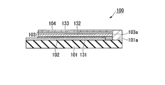
- FIG. 3 is a cross-sectional view showing a laminated structure of a conventional solid junction photoelectric conversion element.
- a general process for forming this laminated structure is to form the first conductive layer 102 on the substrate 101 by a physical vapor deposition method such as a sputtering method, and to form a power generation layer 103 including a perovskite layer by a coating method such as a spin coating method.
- the second conductive layer 104 is formed by a physical vapor deposition method, a printing method, or the like.
- the present invention has been made in view of the above circumstances, and provides a solid junction photoelectric conversion element in which a leak current hardly occurs, and a method for manufacturing the same.
- a solid junction photoelectric conversion element including a base material, a first conductive layer, a power generation layer including a perovskite layer, and a conductive material including a second conductive layer in this order.
- the second conductive layer is a metal foil.
- the solid junction photoelectric conversion element according to [1] or [2], wherein the conductive material is a laminate including the second conductive layer and a support material.
- the power generation layer has one or more cracks extending from the surface on the conductive material side to the first conductive layer side, and the conductive material is in close contact with the power generation layer and straddles the crack.
- the solid junction photoelectric conversion device according to any one of [1] to [5].
- the solid junction photoelectric conversion element of the present invention a leak current hardly occurs even when a stress is applied from the outside to cause bending or distortion. According to the method for producing a solid junction photoelectric conversion element of the present invention, it is possible to easily produce a solid junction photoelectric conversion element in which leakage current hardly occurs.
- film and “layer” are not distinguished unless otherwise specified.
- a solid junction type photoelectric conversion element may be simply referred to as “photoelectric conversion element”
- an organic / inorganic perovskite compound may be simply referred to as “perovskite compound”.
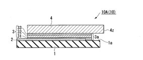
- the solid junction photoelectric conversion element includes a base material 1, a first conductive layer 2, a power generation layer 3 including a perovskite layer 32, and a conductive material including a second conductive layer. 4 in order, and the conductive material 4 has a self-supporting property.
- having self-supporting means that the single conductive material 4 can be handled as a film (planar member).
- Whether or not the conductive material 4 is self-supporting is determined by the following method. For example, a rectangular film (conductive material 4) of 1 mm ⁇ 2 mm in a plan view is prepared, and a half (1 mm ⁇ 1 mm) plane in the longitudinal direction of the film is in contact with the end of a horizontal base. Secure and allow the other half of the membrane to protrude horizontally from the end of the table to the outside of the table. At this time, the end of the base is a straight side, and the short side (tip side) of the protruding film is substantially parallel to this side.
- a method of visually observing whether or not 90% or more of the total area of the protruding portion of the film thus projected is maintained for 10 seconds or more without missing is mentioned.
- 90% or more of the total area of the protrusions is maintained for 10 seconds or more in the above determination method.
- the conductive material does not have self-supporting property, in the above determination method, more than 10% of the total area of the protruding portion is lost within 10 seconds due to its own weight.
- the thickness of the conductive material 4 is 1 ⁇ m or more because the conductive material 4 tends to be self-supporting and easily prevents leakage current. More preferably, it is 2 ⁇ m or more. Specifically, the thickness of the conductive material 4 is preferably 1 ⁇ m to 200 ⁇ m, and more preferably 2 ⁇ m to 100 ⁇ m. When the thickness is 200 ⁇ m or less, the photoelectric conversion element can be easily thinned.
- the thickness T (unit: ⁇ m) of the conductive material 4 and the conductive material 4 The ratio (unit: cm 2 / ⁇ m) expressed by S / T with the area S (unit: cm 2 ) in plan view is preferably, for example, 1 to 1000, more preferably 1 to 500, and 1 to 100. Further preferred.
- thickness is the cross section of the thickness direction of a solid junction type photoelectric conversion element observed with an electron microscope, measured the thickness of arbitrary 10 places of a measuring object, and the arithmetic mean value of each thickness As required.
- the end portion 4 z of the conductive material 4 protruding from the end portion of the power generation layer 3 hardly hangs down due to gravity. Is not in contact with the side surface 3a.
- the second conductive layer 104 is also formed on the side surface 103a of the power generation layer and the surface 101a of the base material. This difference stems from the manufacturing method.
- the solid junction photoelectric conversion element 10 ⁇ / b> A (10) of the first embodiment of the present invention includes a metal foil that forms a conductive material 4 on a power generation layer 3.
- This metal foil is the second conductive layer, and the conductive material 4 is composed of the second conductive layer.
- the thickness of the metal foil is, for example, preferably 1 ⁇ m to 500 ⁇ m, more preferably 2 ⁇ m to 200 ⁇ m, and even more preferably 5 ⁇ m to 100 ⁇ m.
- the thickness is equal to or greater than the lower limit of the thickness range, even if a stress is applied to the photoelectric conversion element and the power generation layer 3 has a crack, a part of the metal foil is difficult to enter the crack, and thus leakage current is generated. Can be prevented.
- the thickness is not more than the upper limit of the thickness range, the metal foil can be prevented from cracking or peeling when stress is applied to the photoelectric conversion element.
- the type of the metal foil is not particularly limited, and for example, any one or more metals selected from the group consisting of gold, silver, copper, aluminum, tungsten, nickel, and chromium are preferable.
- the whole electrically conductive material 4 may be comprised with the conductive polymer.
- the conductive polymer include polyacetylene, poly (p-phenylene), poly (p-phenylene vinylene), polypyrrole, polythiophene, polyethylenedioxythiophene (PEDOT), polythienylene vinylene, polyfluorene, polyaniline, polyacene, A known conductive polymer such as graphene can be used.
- the solid junction photoelectric conversion element 10 ⁇ / b> B (10) of the second embodiment of the present invention includes a conductive material 4 on the power generation layer 3.
- the conductive material 4 is a laminate including a second conductive layer 4a and a support material 4b.
- the thickness of the laminate is, for example, preferably 1 ⁇ m to 500 ⁇ m, more preferably 2 ⁇ m to 200 ⁇ m, and even more preferably 5 ⁇ m to 100 ⁇ m.
- the thickness is equal to or more than the lower limit of the thickness range, even when stress is applied to the photoelectric conversion element and the power generation layer 3 has cracks, the second conductive layer 4a can be sufficiently supported, Since a part of the layer 4a hardly penetrates into the crack, the occurrence of leakage current can be prevented. It can prevent that the 2nd conductive layer 4a is cracked or peeled off when stress is added to a photoelectric conversion element as it is below the upper limit of the range of the said thickness.
- the thickness of the second conductive layer 4a is not particularly limited, and is preferably, for example, 10 nm or more and less than 5 ⁇ m, more preferably 10 nm to 1 ⁇ m, and further preferably 50 nm to 500 nm. If the thickness is equal to or greater than the lower limit of the thickness range, even if stress is applied to the photoelectric conversion element and the power generation layer 3 has a crack, a part of the second conductive layer 4a is difficult to enter the crack. Generation of current can be prevented. Moreover, it can prevent that the resistance of the 2nd conductive layer 4a increases too much, and can reduce the internal resistance of a photoelectric conversion element. It can prevent that the 2nd conductive layer 4a is cracked or peeled off when stress is added to a photoelectric conversion element as it is below the upper limit of the range of the said thickness.
- the material of the 2nd conductive layer 4a is not specifically limited, For example, any 1 or more types of metal selected from the group which consists of gold
- the material of the second conductive layer 4a may be one type or two or more types.
- the shape of the support material 4b is preferably a flat plate shape or a film shape.
- the thickness of the support material 4b is preferably such that the thickness combined with the second conductive layer 4a is 5 ⁇ m or more, for example, preferably 1 ⁇ m to 500 ⁇ m, more preferably 2 ⁇ m to 200 ⁇ m, and even more preferably 5 ⁇ m to 100 ⁇ m.
- the 2nd conductive layer 4a can be supported more stably as it is more than the lower limit of the range of the said thickness. When the thickness is not more than the upper limit value of the thickness range, it is advantageous when flexibility is imparted to the entire photoelectric conversion element.
- the support material 4b is preferably transparent.
- the material of the support material 4b may be an insulating material or a conductive material, but is preferably an insulating material.
- the conductivity of the conductive material 4 can be ensured by the second conductive layer 4a.
- a suitable material for the support member 4b is the same as a suitable material for the substrate 1 described later.
- Substrate 1 The kind in particular of base material 1 is not restrict
- the transparent base material used for the photoelectrode of the conventional solar cell is mentioned.
- the transparent substrate include a substrate made of glass or synthetic resin, a flexible film made of synthetic resin, and the like.
- the material of the transparent substrate is a synthetic resin
- the synthetic resin include polyacrylic resin, polycarbonate resin, polyester resin, polyimide resin, polystyrene resin, polyvinyl chloride resin, and polyamide resin.
- polyester resins particularly polyethylene naphthalate (PEN) and polyethylene terephthalate (PET) are preferable from the viewpoint of manufacturing a thin, light and flexible solar cell.
- the combination of the thickness of the base material 1 and the material is not particularly limited, and examples thereof include a glass substrate having a thickness of 1 mm to 10 mm and a resin film having a thickness of 0.01 mm to 3 mm.
- the material of the 1st conductive layer 2 is not specifically limited, For example, any 1 or more types of metal selected from the group which consists of gold
- the thickness of the first conductive layer 2 is not particularly limited, and is preferably 10 nm to 100 nm, for example.
- the power generation layer 3 is formed in the order of an N-type semiconductor layer (block layer) 31, a perovskite layer (light absorption layer) 32, and a P-type semiconductor layer 33 that are optionally installed on the first conductive layer 2. It is laminated.
- the N-type semiconductor layer 31 is not an essential configuration, the N-type semiconductor layer 31 is preferably disposed between the first conductive layer 2 and the perovskite layer 32.
- the P-type semiconductor layer 33 is not an essential configuration, it is preferable that the P-type semiconductor layer 33 is disposed between the conductive material 4 and the perovskite layer 32.
- the N-type semiconductor layer 31 and the P-type semiconductor layer 33 are preferably non-porous dense layers from the viewpoint of obtaining the above effects.
- the P-type semiconductor layer 33 is formed on the surface of the perovskite layer 32, and the conductive material 4 is formed on the surface of the P-type semiconductor layer 33. preferable.
- the N-type semiconductor constituting the N-type semiconductor layer 31 is not particularly limited, and examples thereof include oxide semiconductors having excellent electron conductivity such as ZnO, TiO 2 , SnO, IGZO, and SrTiO 3 . Of these, TiO 2 is particularly preferable because of its excellent electron conductivity.
- the type of the N-type semiconductor constituting the N-type semiconductor layer 31 may be one type or two or more types.
- the number of layers of the N-type semiconductor layer 31 may be one or may be two or more.
- the total thickness of the N-type semiconductor layer 31 is not particularly limited, but may be about 1 nm to 1 ⁇ m, for example. When the thickness is 1 nm or more, the effect of preventing the loss is sufficiently obtained, and when the thickness is 1 ⁇ m or less, the internal resistance can be kept low.
- the perovskite layer 32 is a layer containing a perovskite compound, and may be formed of only a perovskite compound, or may include an underlayer (not shown) in part or all of the layer.
- the underlayer is a layer that structurally supports the perovskite layer 32.
- the thickness of the perovskite layer 32 is not particularly limited.
- the thickness is preferably 10 nm to 10 ⁇ m, more preferably 50 nm to 1 ⁇ m, and still more preferably 100 nm to 0.5 ⁇ m.
- the light absorption efficiency in the perovskite layer 32 is increased, and more excellent photoelectric conversion efficiency is obtained.
- the efficiency with which the photoelectrons generated in the perovskite layer 32 reach the first conductive layer 2 is increased, and a more excellent photoelectric conversion efficiency is obtained.
- the thickness of the underlayer that may be included in the perovskite layer 32 is not particularly limited, and is preferably 20 to 100%, more preferably 30 to 80%, based on the total thickness of the perovskite layer 32, for example.
- the thickness of the base layer is the thickness from the surface of the N-type semiconductor layer 31.
- the type of the perovskite compound is not particularly limited, and a perovskite compound used in a known solar cell is applicable, has a crystal structure, and exhibits light absorption by bandgap excitation in the same manner as a typical compound semiconductor. Is preferred.
- CH 3 NH 3 PbI 3 which is a known perovskite compound, is known to have an extinction coefficient (cm ⁇ 1 ) per unit thickness that is an order of magnitude higher than that of a sensitizing dye of a dye-sensitized solar cell. Yes.
- the material of the underlayer is preferably an N-type semiconductor and / or an insulator.
- the underlayer may be a porous film or a non-porous dense film, and is preferably a porous film. It is preferable that the perovskite compound is supported by the porous structure of the underlayer. Even when the underlayer is a dense film, it is preferable that the dense film contains a perovskite compound.
- the dense film is preferably formed of an N-type semiconductor.
- the type of the N-type semiconductor that can form the base layer is not particularly limited, and a known N-type semiconductor can be applied.
- a known N-type semiconductor can be applied.
- an oxide that forms a photoelectrode of a conventional dye-sensitized solar cell A semiconductor is mentioned.
- Specific examples include oxide semiconductors excellent in electronic conductivity such as titanium oxide (TiO 2 ), zinc oxide (ZnO), tin oxide (SnO, SnO 2 ), IGZO, strontium titanate (SrTiO 3 ), and the like.
- a compound semiconductor such as Si, Cd, or ZnS doped with a pentavalent element may be used.
- titanium oxide is particularly preferable because of its excellent electron conductivity.
- the N-type semiconductor forming the base layer may be one type or two or more types.
- the kind of the insulator that can form the base layer is not particularly limited, and a known insulator can be applied, and examples thereof include an oxide that forms an insulating layer of a conventional semiconductor device. Specific examples include zirconium dioxide, silicon dioxide, aluminum oxide (AlO, Al 2 O 3 ), magnesium oxide (MgO), nickel oxide (NiO), and the like. Of these, aluminum (III) oxide (Al 2 O 3 ) is particularly preferable.
- the insulator forming the base layer may be one type or two or more types.
- the P-type semiconductor layer 33 formed on the surface of the perovskite layer 32 is composed of a P-type semiconductor.
- the P-type semiconductor layer 33 having holes (holes) is disposed between the perovskite layer 32 and the conductive material 4, the generation of reverse current can be suppressed, and electrons are transferred from the conductive material 4 to the perovskite layer 32.
- the moving efficiency is increased. As a result, the photoelectric conversion efficiency and voltage are increased.
- the kind of the P-type semiconductor is not particularly limited, and may be an organic material or an inorganic material.
- a P-type semiconductor for a hole transport layer of a known solar cell can be applied.
- the organic material include 2,2 ′, 7,7′-tetrakis (N, N-di-p-methoxyphenilamine) -9,9′-spirobifluorene (abbreviation: spiro-OMeTAD), Poly (3-hexylthiophene) (Abbreviation: P3HT), polytriarylamine (abbreviation: PTAA), and the like.
- the inorganic material include copper compounds such as CuI, CuSCN, CuO, and Cu 2 O, and nickel compounds such as NiO.
- the thickness of the P-type semiconductor layer 33 is not particularly limited.
- the thickness is preferably 1 nm to 1000 nm, more preferably 5 nm to 500 nm, and further preferably 30 nm to 500 nm. High electromotive force can be obtained as it is more than the lower limit of the said range. If it is not more than the upper limit of the above range, the internal resistance can be further reduced.
- the method for producing a solid junction photoelectric conversion element of the present invention includes a step of forming a first conductive layer 2 and a power generation layer 3 in this order on a base material 1, and a second conductive layer on the power generation layer 3. And a step of attaching the conductive material 4 including the layer.
- a method of sticking the conductive material 4 on the power generation layer 3 for example, a method of pressing the conductive material 4 placed on the power generation layer 3 is preferable. You may heat simultaneously with a press.
- the area of the conductive material 4 to be attached in plan view is preferably larger than the area of the power generation layer 3 in plan view. With this size, the power generation layer 3 can be easily attached without leaving any excess.
- the base material 1 can be produced by a conventional method, and a commercially available product may be used.
- the method for forming the first conductive layer 2 on the surface of the substrate 1 is not particularly limited, and for example, a known film forming method such as a sputtering method or a vapor deposition method can be applied.
- N-type semiconductor layer 31 is formed on the first conductive layer 2.
- the method for forming the N-type semiconductor layer 31 is not particularly limited, and examples of known methods capable of forming a dense layer made of an N-type semiconductor with a desired thickness include, for example, sputtering, vapor deposition, and dispersion including an N-type semiconductor precursor. Examples thereof include a sol-gel method in which a liquid is applied.
- N-type semiconductor precursors include titanium tetrachloride (TiCl 4 ), peroxotitanic acid (PTA), titanium alkoxide such as titanium ethoxide and titanium isopropoxide (TTIP), zinc alkoxide, alkoxysilane, and zirconium. Examples thereof include metal alkoxides such as alkoxides.
- the method is not particularly limited.
- a conventional method for forming a semiconductor layer carrying a sensitizing dye of a dye-sensitized solar cell can be applied.
- a paste containing fine particles made of an N-type semiconductor or an insulator and a binder is applied to the surface of the N-type semiconductor layer 31 by a doctor blade method, dried, and fired, whereby a porous fine particle made of fine particles is obtained.
- An underlayer can be formed. Further, by spraying fine particles onto the surface of the N-type semiconductor layer 31, a porous or non-porous underlayer made of the fine particles can be formed.
- the method for spraying the fine particles is not particularly limited, and a known method can be applied, for example, an aerosol deposition method (AD method), an electrostatic fine particle coating method (electrostatic spray method) in which fine particles are accelerated by electrostatic force, The cold spray method etc. are mentioned.
- AD method aerosol deposition method
- electrostatic fine particle coating method electrostatic spray method
- the cold spray method etc. are mentioned.
- the AD method is preferable because the speed of the sprayed fine particles can be easily adjusted, the film quality and thickness of the underlying layer to be formed can be easily adjusted, and the film can be formed at a low temperature.
- the method for incorporating the perovskite compound in the underlayer is not particularly limited, for example, a method in which the formed underlayer is impregnated with a solution containing the perovskite compound or a precursor thereof, or a material to which the perovskite compound is previously attached is used. And a method of forming the base layer. The above two methods may be used in combination.
- a raw material to which the perovskite compound crystallized is adhered by immersing the fine particles in a raw material solution in which a perovskite compound or a precursor of the perovskite compound is dissolved and further drying the solvent.
- grains is mentioned.
- a layer (upper layer) containing a perovskite compound may be further formed on the surface of the underlayer.
- the method for forming the upper layer is not particularly limited, and examples thereof include the following method. That is, a raw material solution in which a perovskite compound or a perovskite compound precursor is dissolved is applied to the surface of the base layer, the raw material solution is impregnated inside the base layer, and the surface of the base layer has a desired thickness. In this method, the solvent is dried in a state where there is a solution layer made of the raw material solution.
- At least a part of the raw material solution applied to the base layer penetrates into the porous film of the base layer, and crystallization proceeds with drying of the solvent, and a perovskite compound adheres and deposits in the porous film. Further, by applying a sufficient amount of the raw material solution, the raw material solution that has not penetrated into the porous film forms the upper layer made of a perovskite compound on the surface of the underlayer together with the drying of the solvent.
- the perovskite compound constituting the upper layer and the perovskite compound inside the underlayer are integrally formed, and the perovskite layer 32 is integrally formed.
- the perovskite compound used in the present embodiment is not particularly limited as long as it can generate an electromotive force by light absorption, and a known perovskite compound is applicable.
- perovskite-type crystals can be formed, and the following composition formula (1) having an organic component and an inorganic component in a single compound: ABX 3 (1)
- the perovskite compound represented by these is preferable.
- A represents an organic cation
- B represents a metal cation
- X represents a halogen ion.
- the B site can take octahedral coordination with the X site. It is considered that the metal cation at the B site and the atomic orbital of the halogen ion at the X site are mixed to form a valence band and a conduction band related to photoelectric conversion.
- the metal constituting the metal cation represented by B in the composition formula (1) is not particularly limited, and examples thereof include Cu, Ni, Mn, Fe, Co, Pd, Ge, Sn, Pb, and Eu. Among these, Pb and Sn are preferable because they can easily form a highly conductive band by hybridization with the atomic orbitals of halogen ions at the X site.
- the metal cation constituting the B site may be one type or two or more types.
- the halogen constituting the halogen ion represented by X in the composition formula (1) is not particularly limited, and examples thereof include F, Cl, Br, and I. Among these, Cl, Br, and I are preferable because they can easily form a highly conductive band by a hybrid orbital with a metal cation at the B site. There may be one kind of halogen ion constituting the X site, or two or more kinds.
- the organic group constituting the organic cation represented by A in the composition formula (1) is not particularly limited, and examples thereof include alkylammonium derivatives and formamidinium derivatives.
- the organic cation constituting the A site may be one type or two or more types.
- Examples of the organic cation formed by the alkyl ammonium derivative include carbon such as methyl ammonium, dimethyl ammonium, trimethyl ammonium, ethyl ammonium, propyl ammonium, isopropyl ammonium, tert-butyl ammonium, pentyl ammonium, hexyl ammonium, octyl ammonium, and phenyl ammonium.
- Examples thereof include primary or secondary ammonium having a number 1 to 6 alkyl group. Of these, methylammonium, which can easily obtain perovskite crystals, is preferred.
- formamidinium derivative examples include formamidinium, methylformamidinium, dimethylformamidinium, trimethylformamidinium, and tetramethylformamidinium. Of these, formamidinium is preferred because it can easily obtain a perovskite crystal.
- a suitable perovskite compound represented by the composition formula (1) for example, CH 3 NH 3 PbI 3 , CH 3 NH 3 PbI 3-h Cl h (h represents 0 to 3), CH 3 NH 3 PbI.
- the following composition formula (2) such as 3-j Br j (j represents 0 to 3): RNH 3 PbX 3 (2)
- R represents an alkyl group
- X represents a halogen ion. Since the perovskite compound having this composition formula has a wide absorption wavelength range and can absorb a wide wavelength range of sunlight, excellent photoelectric conversion efficiency can be obtained.
- the alkyl group represented by R in the composition formula (2) is preferably a linear, branched or cyclic saturated or unsaturated alkyl group having 1 to 6 carbon atoms, and a straight chain having 1 to 6 carbon atoms.
- a chain saturated alkyl group is more preferable, and a methyl group, an ethyl group, or an n-propyl group is further preferable. With these preferable alkyl groups, perovskite crystals can be easily obtained.
- examples of the precursor contained in the raw material solution include a halide (BX) containing a metal ion at the B site and a halogen ion at the X site, and an organic at the A site. And halide (AX) containing a cation and a halogen ion at the X site.
- a single raw material solution containing halide (AX) and halide (BX) may be applied to the underlayer, or two raw material solutions containing each halide individually may be applied in turn to the underlayer. You may apply to.
- the solvent of the raw material solution is not particularly limited as long as it is a solvent that dissolves the raw material and does not damage the underlying layer.
- a solvent that dissolves the raw material and does not damage the underlying layer for example, ester, ketone, ether, alcohol, glycol ether, amide, nitrile, carbonate, halogenated hydrocarbon , Hydrocarbons, sulfones, sulfoxides, formamides and the like.
- an alkylamine halide and a lead halide are dissolved in a mixed solvent of ⁇ -butyrolactone (GBL) and dimethyl sulfoxide (DMSO), and the solution is applied to the underlayer and dried, whereby the composition formula (2
- GBL ⁇ -butyrolactone
- DMSO dimethyl sulfoxide
- a solvent that does not dissolve the perovskite crystal and is miscible with GBL or DMSO, such as toluene or chloroform is applied at about 100 ° C.
- An annealing process may be added. This additional treatment may improve the stability of the perovskite crystal and increase the photoelectric conversion efficiency.
- the concentration of the raw material in the raw material solution is not particularly limited, and is preferably a concentration that is sufficiently dissolved and exhibits a viscosity that allows the raw material solution to penetrate into the porous membrane.
- the amount of the raw material solution applied to the undercoat layer is not particularly limited.
- the upper solution having a thickness of about 1 nm to 1 ⁇ m permeates the whole or at least a part of the porous film.
- a coating amount sufficient to form a layer is preferable.
- the method for applying the raw material solution to the underlayer is not particularly limited, and a known method such as a gravure coating method, a bar coating method, a printing method, a spray method, a spin coating method, a dip method, or a die coating method can be applied.
- a method for drying the raw material solution applied to the base layer is not particularly limited, and a known method such as natural drying, reduced pressure drying, hot air drying, or the like can be applied.
- the drying temperature of the raw material solution applied to the underlayer may be a temperature at which the crystallization of the perovskite compound proceeds sufficiently, and may be in the range of 40 to 150 ° C., for example.
- the method for forming the P-type semiconductor layer 33 is not particularly limited.
- a solution in which a P-type semiconductor is dissolved or dispersed in a solvent that hardly dissolves the perovskite compound constituting the perovskite layer 32 is prepared.
- the method of obtaining the P-type semiconductor layer 33 by applying to the surface and drying is used.
- the power generation layer 3 including the N-type semiconductor layer 31, the perovskite layer 32, and the P-type semiconductor layer 33 in this order can be formed.
- Example 1 A transparent resin substrate (PEN substrate) having a transparent conductive layer made of ITO formed on the surface thereof was prepared. A part of this ITO layer was etched using hydrochloric acid. The purpose of this etching is to leave only the region for forming the power generation layer and the region necessary for the lead wiring out of the ITO layer formed on the entire surface of the PEN substrate, and to remove other unnecessary regions. Subsequently, a DMF solution in which 1M CH 3 NH 3 PbI 3 was dissolved was spin-coated on the PEN substrate, and heated and dried at 100 ° C. for 90 minutes to form a perovskite layer (power generation layer).
- a DMF solution in which 1M CH 3 NH 3 PbI 3 was dissolved was spin-coated on the PEN substrate, and heated and dried at 100 ° C. for 90 minutes to form a perovskite layer (power generation layer).
- a gold foil (Au foil) having a thickness of 10 ⁇ m having a self-supporting property was placed on the perovskite layer, and the gold foil and the PEN substrate were sandwiched between clips, thereby pressing the gold foil to the power generation layer.
- the frequency (leakage frequency) at which leakage current occurs was evaluated by the following method. As a result, 16 pieces passed and 4 pieces failed. In other words, leak current was generated in 4 of the 20 manufactured solid junction photoelectric conversion elements, and the leak frequency was 20%.
- Example 2 to 5 A photoelectric conversion element was produced and evaluated in the same manner as in Example 1 except that a Ti foil, Al foil, or Ag foil having a thickness of 50 ⁇ m having a self-supporting property was used instead of the Au foil. The results are shown in Table 1.
- Example 6 In place of Au foil, except that a self-supporting conductive material in which a 0.1 ⁇ m thick Au layer, Ti layer, Al layer, and Ag layer were formed on the surface of a 125 ⁇ m thick PEN film was used. A photoelectric conversion element was prepared and evaluated in the same manner as in Example 1. The results are shown in Table 1.
- the solid junction photoelectric conversion element according to the present invention is less prone to leak current and is manufactured with a high yield.
- the cause is the roughness of ITO deposited on the PEN substrate and the press (crimping) conditions. .
- the solid junction photoelectric conversion element of the present invention a leak current hardly occurs even when a stress is applied from the outside to cause bending or distortion. According to the method for producing a solid junction photoelectric conversion element of the present invention, it is possible to easily produce a solid junction photoelectric conversion element in which leakage current hardly occurs.
- DESCRIPTION OF SYMBOLS 1 ... Base material, 2 ... 1st conductive layer, 3 ... Power generation layer, 3a ... Side surface of power generation layer, 4 ... Conductive material, 4a ... 2nd conductive layer, 4b ... Support material, 10 ... Solid junction type photoelectric conversion element, DESCRIPTION OF SYMBOLS 31 ... N-type semiconductor layer, 32 ... Perovskite layer, 33 ... P-type semiconductor layer, 100 ... Solid junction photoelectric conversion element of comparative example, 101 ... Base material, 101a ... Surface of base material, 102 ... First conductive layer, DESCRIPTION OF SYMBOLS 103 ... Power generation layer, 103a ... Side surface of power generation layer, 104 ... Second conductive layer, 131 ... N type semiconductor layer, 132 ... Perovskite layer, 133 ... P type semiconductor layer
Landscapes
- Engineering & Computer Science (AREA)
- Chemical & Material Sciences (AREA)
- Chemical Kinetics & Catalysis (AREA)
- Electrochemistry (AREA)
- Power Engineering (AREA)
- Physics & Mathematics (AREA)
- Electromagnetism (AREA)
- Materials Engineering (AREA)
- Microelectronics & Electronic Packaging (AREA)
- Manufacturing & Machinery (AREA)
- Photovoltaic Devices (AREA)
Priority Applications (4)
| Application Number | Priority Date | Filing Date | Title |
|---|---|---|---|
| US16/065,931 US20190013155A1 (en) | 2016-02-19 | 2017-02-17 | Solid junction-type photovoltaic device and method for producing same |
| CN201780005226.2A CN108475729A (zh) | 2016-02-19 | 2017-02-17 | 固体接合型光电转换元件及其制造方法 |
| EP17753328.8A EP3419068A4 (de) | 2016-02-19 | 2017-02-17 | Fester photoelektrischer übergangswandler und verfahren zur herstellung davon |
| JP2018500228A JPWO2017142074A1 (ja) | 2016-02-19 | 2017-02-17 | 固体接合型光電変換素子、及びその製造方法 |
Applications Claiming Priority (2)
| Application Number | Priority Date | Filing Date | Title |
|---|---|---|---|
| JP2016029952 | 2016-02-19 | ||
| JP2016-029952 | 2016-02-19 |
Publications (1)
| Publication Number | Publication Date |
|---|---|
| WO2017142074A1 true WO2017142074A1 (ja) | 2017-08-24 |
Family
ID=59626018
Family Applications (1)
| Application Number | Title | Priority Date | Filing Date |
|---|---|---|---|
| PCT/JP2017/005959 Ceased WO2017142074A1 (ja) | 2016-02-19 | 2017-02-17 | 固体接合型光電変換素子、及びその製造方法 |
Country Status (6)
| Country | Link |
|---|---|
| US (1) | US20190013155A1 (de) |
| EP (1) | EP3419068A4 (de) |
| JP (1) | JPWO2017142074A1 (de) |
| CN (1) | CN108475729A (de) |
| TW (1) | TW201801366A (de) |
| WO (1) | WO2017142074A1 (de) |
Cited By (1)
| Publication number | Priority date | Publication date | Assignee | Title |
|---|---|---|---|---|
| WO2023038103A1 (ja) * | 2021-09-10 | 2023-03-16 | 株式会社Gceインスティチュート | 発電素子、発電素子の製造方法、発電装置、及び電子機器 |
Families Citing this family (2)
| Publication number | Priority date | Publication date | Assignee | Title |
|---|---|---|---|---|
| US12195348B2 (en) * | 2018-09-06 | 2025-01-14 | King Abdullah University Of Science And Technology | Method for making inorganic perovskite nanocrystals film and applications |
| WO2021153218A1 (ja) * | 2020-01-31 | 2021-08-05 | 日本ゼオン株式会社 | 光電変換素子及びその製造方法 |
Citations (7)
| Publication number | Priority date | Publication date | Assignee | Title |
|---|---|---|---|---|
| JP2006237165A (ja) * | 2005-02-23 | 2006-09-07 | Sharp Corp | 有機太陽電池モジュール及びその製造方法 |
| JP2011142217A (ja) * | 2010-01-07 | 2011-07-21 | Dainippon Printing Co Ltd | 有機薄膜太陽電池 |
| WO2012053373A1 (ja) * | 2010-10-22 | 2012-04-26 | リンテック株式会社 | 導電性粘着剤組成物、電子デバイス及び電子デバイスの製造方法 |
| JP2012124336A (ja) * | 2010-12-08 | 2012-06-28 | Dainippon Printing Co Ltd | 有機薄膜太陽電池の製造方法 |
| JP2013225447A (ja) * | 2012-04-23 | 2013-10-31 | Mitsui Mining & Smelting Co Ltd | 電極箔及び電子デバイス |
| JP2014229747A (ja) * | 2013-05-22 | 2014-12-08 | ペクセル・テクノロジーズ株式会社 | ペロブスカイト化合物を用いた光電変換素子およびその製造方法 |
| JP2014236065A (ja) * | 2013-05-31 | 2014-12-15 | 三井化学株式会社 | 有機薄膜太陽電池の製造方法および有機薄膜太陽電池 |
Family Cites Families (7)
| Publication number | Priority date | Publication date | Assignee | Title |
|---|---|---|---|---|
| JP2013136502A (ja) * | 2011-11-28 | 2013-07-11 | Mitsubishi Materials Corp | 強誘電体薄膜形成用組成物及びその薄膜の形成方法並びにその方法で形成された薄膜 |
| WO2014165830A2 (en) * | 2013-04-04 | 2014-10-09 | The Regents Of The University Of California | Electrochemical solar cells |
| EP2808913A1 (de) * | 2013-05-31 | 2014-12-03 | Swansea University | Laminierte optoelektronische Vorrichtung und Verfahren zu deren Herstellung |
| CN104134752B (zh) * | 2014-07-08 | 2017-02-08 | 中国科学院物理研究所 | 钙钛矿太阳能电池及其热塑性碳对电极的制备方法 |
| GB201412201D0 (en) * | 2014-07-09 | 2014-08-20 | Isis Innovation | Two-step deposition process |
| WO2016014845A1 (en) * | 2014-07-23 | 2016-01-28 | The University Of Akron | Ultrasensitive solution-processed perovskite hybrid photodetectors |
| CN104993054B (zh) * | 2015-05-14 | 2018-01-16 | 大连理工大学 | 一种新型叠合式钙钛矿太阳能电池的制备方法 |
-
2017
- 2017-02-17 US US16/065,931 patent/US20190013155A1/en not_active Abandoned
- 2017-02-17 WO PCT/JP2017/005959 patent/WO2017142074A1/ja not_active Ceased
- 2017-02-17 JP JP2018500228A patent/JPWO2017142074A1/ja active Pending
- 2017-02-17 EP EP17753328.8A patent/EP3419068A4/de not_active Withdrawn
- 2017-02-17 TW TW106105258A patent/TW201801366A/zh unknown
- 2017-02-17 CN CN201780005226.2A patent/CN108475729A/zh active Pending
Patent Citations (7)
| Publication number | Priority date | Publication date | Assignee | Title |
|---|---|---|---|---|
| JP2006237165A (ja) * | 2005-02-23 | 2006-09-07 | Sharp Corp | 有機太陽電池モジュール及びその製造方法 |
| JP2011142217A (ja) * | 2010-01-07 | 2011-07-21 | Dainippon Printing Co Ltd | 有機薄膜太陽電池 |
| WO2012053373A1 (ja) * | 2010-10-22 | 2012-04-26 | リンテック株式会社 | 導電性粘着剤組成物、電子デバイス及び電子デバイスの製造方法 |
| JP2012124336A (ja) * | 2010-12-08 | 2012-06-28 | Dainippon Printing Co Ltd | 有機薄膜太陽電池の製造方法 |
| JP2013225447A (ja) * | 2012-04-23 | 2013-10-31 | Mitsui Mining & Smelting Co Ltd | 電極箔及び電子デバイス |
| JP2014229747A (ja) * | 2013-05-22 | 2014-12-08 | ペクセル・テクノロジーズ株式会社 | ペロブスカイト化合物を用いた光電変換素子およびその製造方法 |
| JP2014236065A (ja) * | 2013-05-31 | 2014-12-15 | 三井化学株式会社 | 有機薄膜太陽電池の製造方法および有機薄膜太陽電池 |
Non-Patent Citations (2)
| Title |
|---|
| "Efficient Hybrid Solar Cells Based on Meso-Superstructured Organometal Halide Perovskites", SCIENCE, vol. 338, 2012, pages 643 - 647 |
| "Solvent engineering for high-performance inorganic-organic hybrid perovskite solar cells", NATURE MATERIALS, vol. 13, 2014, pages 897 - 903 |
Cited By (1)
| Publication number | Priority date | Publication date | Assignee | Title |
|---|---|---|---|---|
| WO2023038103A1 (ja) * | 2021-09-10 | 2023-03-16 | 株式会社Gceインスティチュート | 発電素子、発電素子の製造方法、発電装置、及び電子機器 |
Also Published As
| Publication number | Publication date |
|---|---|
| CN108475729A (zh) | 2018-08-31 |
| JPWO2017142074A1 (ja) | 2018-12-20 |
| EP3419068A1 (de) | 2018-12-26 |
| US20190013155A1 (en) | 2019-01-10 |
| EP3419068A4 (de) | 2019-10-02 |
| TW201801366A (zh) | 2018-01-01 |
Similar Documents
| Publication | Publication Date | Title |
|---|---|---|
| JP6849673B2 (ja) | 固体接合型光電変換素子、及びその製造方法 | |
| JP7389018B2 (ja) | Sn系ペロブスカイト層及び太陽電池の製造方法 | |
| US20180369861A1 (en) | Film forming method | |
| JP6206855B2 (ja) | 半導体素子及び太陽電池 | |
| US20140202527A1 (en) | Solar cell and method of manufacturing the solar cell | |
| WO2016002211A1 (en) | Surface-passivated mesoporous structure solar cell | |
| JP2016502282A (ja) | ペロブスカイトショットキー型太陽電池 | |
| TW201607092A (zh) | 有機-無機串疊型太陽能電池 | |
| Yang et al. | An annealing-free aqueous-processed anatase TiO 2 compact layer for efficient planar heterojunction perovskite solar cells | |
| CN108431982B (zh) | 固体接合型光电转换元件模块及其制造方法 | |
| Hsieh et al. | Ultra-compact titanium oxide prepared by ultrasonic spray pyrolysis method for planar heterojunction perovskite hybrid solar cells | |
| KR101458565B1 (ko) | 유기 태양전지 및 이의 제조방법 | |
| WO2017142074A1 (ja) | 固体接合型光電変換素子、及びその製造方法 | |
| JP2016178167A (ja) | 光電極の製造方法、光電極、太陽電池の製造方法および太陽電池 | |
| TW201826554A (zh) | 固體接合型光電轉換元件、鈣鈦礦膜及光電轉換模組 | |
| JP2017028027A (ja) | 固体接合型光電変換素子および固体接合型光電変換素子用p型半導体層 | |
| Pintilie et al. | Properties of perovskite ferroelectrics deposited on F doped SnO2 electrodes and the prospect of their integration into perovskite solar cells | |
| JP2019175918A (ja) | 光電変換素子及び太陽電池モジュール | |
| JP2018157147A (ja) | 固体接合型光電変換素子 | |
| Yi et al. | Enhanced interface of polyurethane acrylate via perfluoropolyether for efficient transfer printing and stable operation of PEDOT: PSS in perovskite photovoltaic cells | |
| JP7007114B2 (ja) | 固体接合型光電変換素子 | |
| JP2018117008A (ja) | 固体接合型光電変換素子および固体接合型光電変換素子用のp型半導体層 | |
| JP6739729B2 (ja) | 光電変換素子の製造方法 | |
| JP2016178166A (ja) | 光電極の製造方法、光電極、太陽電池の製造方法および太陽電池 | |
| JP2017028028A (ja) | 固体接合型光電変換素子および固体接合型光電変換素子用p型半導体層 |
Legal Events
| Date | Code | Title | Description |
|---|---|---|---|
| 121 | Ep: the epo has been informed by wipo that ep was designated in this application |
Ref document number: 17753328 Country of ref document: EP Kind code of ref document: A1 |
|
| WWE | Wipo information: entry into national phase |
Ref document number: 2018500228 Country of ref document: JP |
|
| NENP | Non-entry into the national phase |
Ref country code: DE |
|
| WWE | Wipo information: entry into national phase |
Ref document number: 2017753328 Country of ref document: EP |
|
| ENP | Entry into the national phase |
Ref document number: 2017753328 Country of ref document: EP Effective date: 20180919 |