WO2017145505A1 - 無線icデバイスおよび無線icデバイスの製造方法 - Google Patents
無線icデバイスおよび無線icデバイスの製造方法 Download PDFInfo
- Publication number
- WO2017145505A1 WO2017145505A1 PCT/JP2016/087703 JP2016087703W WO2017145505A1 WO 2017145505 A1 WO2017145505 A1 WO 2017145505A1 JP 2016087703 W JP2016087703 W JP 2016087703W WO 2017145505 A1 WO2017145505 A1 WO 2017145505A1
- Authority
- WO
- WIPO (PCT)
- Prior art keywords
- diameter
- small
- conductor
- conductor pattern
- loop
- Prior art date
- Legal status (The legal status is an assumption and is not a legal conclusion. Google has not performed a legal analysis and makes no representation as to the accuracy of the status listed.)
- Ceased
Links
Images


Classifications
-
- G—PHYSICS
- G06—COMPUTING OR CALCULATING; COUNTING
- G06K—GRAPHICAL DATA READING; PRESENTATION OF DATA; RECORD CARRIERS; HANDLING RECORD CARRIERS
- G06K19/00—Record carriers for use with machines and with at least a part designed to carry digital markings
- G06K19/06—Record carriers for use with machines and with at least a part designed to carry digital markings characterised by the kind of the digital marking, e.g. shape, nature, code
- G06K19/067—Record carriers with conductive marks, printed circuits or semiconductor circuit elements, e.g. credit or identity cards also with resonating or responding marks without active components
- G06K19/07—Record carriers with conductive marks, printed circuits or semiconductor circuit elements, e.g. credit or identity cards also with resonating or responding marks without active components with integrated circuit chips
- G06K19/077—Constructional details, e.g. mounting of circuits in the carrier
-
- H—ELECTRICITY
- H01—ELECTRIC ELEMENTS
- H01P—WAVEGUIDES; RESONATORS, LINES, OR OTHER DEVICES OF THE WAVEGUIDE TYPE
- H01P11/00—Apparatus or processes specially adapted for manufacturing waveguides or resonators, lines, or other devices of the waveguide type
-
- H—ELECTRICITY
- H01—ELECTRIC ELEMENTS
- H01Q—ANTENNAS, i.e. RADIO AERIALS
- H01Q1/00—Details of, or arrangements associated with, antennas
- H01Q1/12—Supports; Mounting means
- H01Q1/22—Supports; Mounting means by structural association with other equipment or articles
- H01Q1/24—Supports; Mounting means by structural association with other equipment or articles with receiving set
-
- H—ELECTRICITY
- H01—ELECTRIC ELEMENTS
- H01Q—ANTENNAS, i.e. RADIO AERIALS
- H01Q1/00—Details of, or arrangements associated with, antennas
- H01Q1/40—Radiating elements coated with or embedded in protective material
-
- H—ELECTRICITY
- H01—ELECTRIC ELEMENTS
- H01Q—ANTENNAS, i.e. RADIO AERIALS
- H01Q7/00—Loop antennas with a substantially uniform current distribution around the loop and having a directional radiation pattern in a plane perpendicular to the plane of the loop
Definitions
- the present invention relates to a wireless IC device including a helical coil used in a short-range wireless communication apparatus such as an RFID (Radio Frequency Identification) tag.
- a wireless IC device including a helical coil used in a short-range wireless communication apparatus such as an RFID (Radio Frequency Identification) tag.
- RFID Radio Frequency Identification
- HF band RFID tags are generally card-sized, but small RFID tags with a small occupied area may be required for use in merchandise management.
- a small HF band RFID tag an RFID tag having a shape as shown in Patent Documents 1 and 2 is known.
- These small-sized RFID tags are RFID tags using a so-called sheet lamination method, in which a laminated helical coil (coil antenna) is built in a multilayer substrate, and an RFIC chip is mounted on the multilayer substrate.
- JP 2007-102348 A International Publication No. 2011/108340
- the RFID tags shown in Patent Documents 1 and 2 are arranged at a position where the main surface of the RFIC chip intersects the central axis of the helical coil. Therefore, an electrode (land pattern) for mounting the RFIC chip intersects with the winding axis of the helical coil. As a result, the RFIC chip mounting electrode and the RFIC chip tend to prevent the magnetic field from being formed by the helical coil. If the RFIC chip is arranged outside the coil opening, it is difficult to prevent the formation of the magnetic field, but the volume is increased.
- the wireless IC device (101) of the present invention is A resin body (10) having a first surface (VS1) and a second surface (VS2) facing the first surface (VS1); A winding shaft having a first part embedded in the resin body (10) and a second part patterned on the surface of the resin body (10) and along the first surface (VS1) A helical coil (HC1) having (AX); A first insulating layer (1); RFIC (4) connected to the helical coil (HC1); With The helical coil (HC1) Large diameter loops (BL1, BL2, BL3, BL4); The outer diameter of the large-diameter loop (BL1, BL2, BL3, BL4) is conducted to the large-diameter loop (BL1, BL2, BL3, BL4) and viewed from the winding axis (AX) direction (Y-axis direction).
- the second portion is formed on the first surface (VS1), and includes a first large-diameter conductor pattern (Bp11, Bp12, Bp13, Bp14) that constitutes a part of the large-diameter loop (BL1, BL2, BL3, BL4).
- the first insulating layer (1) is sandwiched at least at a portion where the first large-diameter conductor pattern (Bp11, Bp12, Bp13, Bp14) and the first small-diameter conductor pattern (Sp11, Sp12, Sp13, Sp14) overlap. It is characterized by that.
- the small-diameter conductor pattern and the large-diameter conductor pattern are not formed on the same plane, and an insulating layer is interposed between the small-diameter conductor pattern and the large-diameter conductor pattern.
- the possibility of contact with the conductor pattern (short circuit between lines) is low. Therefore, insulation between the large-diameter conductor pattern and the small-diameter conductor pattern is ensured without separately providing a connection member such as a jumper chip. Therefore, the large-diameter loop and the small-diameter loop can be arranged at a narrow pitch in the winding axis direction, and a helical coil having a desired number of turns and a desired inductance value can be easily obtained.
- the small-diameter conductor pattern and the large-diameter conductor pattern partially overlap each other when viewed from the direction orthogonal to the first surface. Therefore, the line width of the small-diameter conductor pattern and the large-diameter conductor pattern can be easily increased, and the helical The DCR of the coil can be further reduced.
- At least a part of the large-diameter loop and the small-diameter loop constituting the helical coil is made of a metal member (columnar conductor). Therefore, the DCR of the large-diameter loop and the small-diameter loop can be reduced as compared with the case where the sintered metal body is formed by firing the conductive paste, or the thin-film metal body is formed by etching the conductive thin film. A lossy helical coil is obtained. Further, since the resistance of the entire helical coil can be reduced, a highly sensitive wireless IC device or a small wireless IC device for high sensitivity can be obtained.
- the second portion is formed on the second surface, and is formed on the second surface with a second small-diameter conductor pattern constituting a part of the small-diameter loop, and the large-diameter A second large-diameter conductor pattern that constitutes a part of the loop may be included.
- the second insulating layer is sandwiched at least in a portion where the second large-diameter conductor pattern and the second small-diameter conductor pattern overlap.
- the small-diameter conductor pattern and the large-diameter conductor pattern partially overlap each other when viewed from the direction orthogonal to the first surface, the line width of the small-diameter conductor pattern and the large-diameter conductor pattern can be easily increased, and the helical coil DCR can be further reduced.
- the wireless IC device of the present invention A resin body (10) having a first surface (VS1) and a second surface (VS2) facing the first surface (VS1); A winding shaft having a first part embedded in the resin body (10) and a second part patterned on the surface of the resin body (10) and along the first surface (VS1) A helical coil (HC1) having (AX); RFIC (4) connected to the helical coil (HC1); With The helical coil (HC1) Large diameter loops (BL1, BL2, BL3, BL4); Conducted to the large-diameter loops (BL1, BL2, BL3, BL4), and viewed from the winding axis direction (Y-axis direction), inside the outer diameter of the large-diameter loops (BL1, BL2, BL3, BL4) A small-diameter loop (SL1, SL2, SL3, SL4) disposed; With The first portion includes a large-diameter U-shaped conductor (Bb1 or the like) that is
- the second portion is formed on the first surface (VS1), and a first large-diameter conductor pattern (Bp11, Bp12, etc.) constituting a part of the large-diameter loop (BL1, BL2, BL3, BL4), A first small-diameter conductor pattern (Sp13, Sp14, etc.) formed on the first surface and constituting a part of the small-diameter loop (SL1, SL2, SL3, SL4);
- the first insulating layer (1) is sandwiched between at least a portion where the first large-diameter conductor pattern (Bp11, Bp12, etc.) and the first small-diameter conductor pattern (Sp13, Sp14, etc.) overlap.
- the large-diameter loop and the small-diameter loop constituting the helical coil is made of a metal member (U-shaped conductor). Therefore, the DCR of the large-diameter loop and the small-diameter loop can be reduced as compared with the case where the sintered metal body is formed by firing the conductive paste, or the thin-film metal body is formed by etching the conductive thin film. A lossy helical coil is obtained. Further, since the resistance of the entire helical coil can be reduced, a highly sensitive wireless IC device or a small wireless IC device for high sensitivity can be obtained.
- the circuit board further includes a wiring board having a first main surface and a second main surface, and the wiring board has the second main surface inside the resin main body.
- the RFIC is mounted on the second main surface, and at least a part of the RFIC is embedded in the resin main body.
- the large-diameter loop and the small-diameter loop are arranged without gaps along the winding axis direction when the second surface is viewed in plan. Is preferred. With this configuration, the magnetic flux generated in the helical coil is hardly leaked from the gap between the large-diameter loop and the small-diameter loop adjacent to each other. Therefore, a helical coil having a high inductance value can be configured.
- the large-diameter loop and the small-diameter loop are viewed from a direction parallel to the first surface and a direction orthogonal to the winding axis direction, It is preferable that they are arranged without gaps along the winding axis direction. With this configuration, the magnetic flux generated in the helical coil is difficult to leak from the gap between the large-diameter loop and the small-diameter loop that are adjacent to each other. Therefore, a helical coil having a high inductance value can be configured.
- the helical coil includes the large-diameter loop and the small-diameter loop arranged alternately in the winding axis direction and alternately connected It is preferable to be configured. With this configuration, a helical coil having a small occupation area (especially a dimension in the direction of the winding axis) can be realized for the number of turns. Also, with this configuration, the conductor that does not contribute to inductance can be shortened, so that the DCR of the helical coil can be further reduced.
- the number of the large diameter loops and the number of the small diameter loops are plural, and the plurality of large diameter loops are connected to each other to form a helical large diameter
- the plurality of small diameter loops are connected to each other to form a helical small diameter coil, and the helical coil is configured by connecting the small diameter coil to the large diameter coil.
- the extending direction from the first end of the large-diameter coil to the second end in the winding axis direction is from the first end to the second end of the small-diameter coil in the winding axis direction.
- the second end of the large-diameter coil is connected to the first end of the small-diameter coil, and at least a part of the formation area of the large-diameter coil in the winding axis direction. Preferably overlaps with the formation region of the small-diameter coil in the winding axis direction.
- a resin main body having a first surface and a second surface facing the first surface;
- a small-diameter loop composed of a first small-diameter columnar conductor, a second small-diameter columnar conductor, a first small-diameter conductor pattern, and a second small-diameter conductor pattern, a first large-diameter columnar conductor, a second large-diameter columnar conductor, and a first large-diameter conductor
- a helical coil having a pattern and a large diameter loop composed of a second large diameter conductor pattern;
- RFIC connected to the helical coil; With At least a portion where the first large-diameter conductor pattern and the first small-diameter conductor pattern overlap each other, a first insulating layer is sandwiched between them, The method of manufacturing the wireless IC device of the present invention, in which the second insulating layer is sandwiched at least in a portion where the second large diameter conduct
- a sixth step of forming the second large-diameter conductor pattern After the third step, a seventh step of removing the support base from the resin body; After the seventh step, the first small-diameter conductor pattern connected to at least one of the first end of the first small-diameter columnar conductor or the first end of the second small-diameter columnar conductor is formed on the first surface.
- a wireless IC device including a small helical coil having a desired inductance value and excellent electrical characteristics, and particularly capable of reducing DC resistance.
- a resin body having a first surface and a second surface facing the first surface;
- a helical coil having a small-diameter loop composed of a small-diameter U-shaped conductor and a first small-diameter conductor pattern, and a large-diameter loop composed of a large-diameter U-shaped conductor and a first large-diameter conductor pattern;
- RFIC connected to the helical coil;
- a twelfth step After the twelfth step, a thirteenth step of removing the support base from the resin body; After the thirteenth step, a fourteenth step of forming the first small-diameter conductor pattern connected to one end of the small-diameter U-shaped conductor on the first surface; A fifteenth step of forming the first insulating layer on at least part of the surface of the first small-diameter conductor pattern after the fourteenth step; A sixteenth step of forming the first large-diameter conductor pattern connected to one end of the large-diameter U-shaped conductor on the first surface and the surface of the first insulating layer after the fifteenth step; It is characterized by providing.
- a wireless IC device including a small helical coil having a desired inductance value and further excellent electrical characteristics, and particularly capable of reducing DC resistance.
- the wireless IC device is a resin block in which the first small-diameter columnar conductor, the second small-diameter columnar conductor, the first large-diameter columnar conductor, and the second large-diameter columnar conductor are embedded. It is preferable that the second step further includes a step of mounting the resin block on the support base. According to the above manufacturing method, since the resin block in which the columnar conductors are embedded beforehand is used, it is not necessary to consider contact between adjacent columnar conductors when the columnar conductors are built on the support base. Therefore, a wireless IC device in which the gap between adjacent columnar conductors is small can be easily realized.
- the first step is performed on the second main surface of the wiring board having a first main surface and a second main surface opposite to the first main surface.
- the step of mounting the RFIC and the step of mounting the first main surface side on the support base may be further included.
- the support base has an adhesive layer on a main surface
- the first step further includes a step of fixing the first main surface side of the wiring board with the adhesive layer side. You may do it.
- the support base has an adhesive layer on a main surface
- the second step includes the first small-diameter columnar conductor, the second small-diameter columnar conductor, the first large-diameter columnar conductor
- the method further includes a step of fixing the first end of each of the second large-diameter columnar conductors to the adhesive layer side.
- a columnar conductor can be firmly fixed by using the support stand which has an adhesion layer. Therefore, a columnar conductor having a small diameter can also be used for manufacturing a helical coil, and a helical coil having a large number of turns and high inductance can be manufactured.
- the support base has an adhesive layer on a main surface, and the eleventh step is configured so that both ends of the large-diameter U-shaped conductor and the small-diameter U-shaped conductor are bonded to the adhesive. It is preferable to further include a step of fixing on the layer side.
- a large diameter U-shaped conductor and a small diameter U-shaped conductor can be firmly fixed by using the support stand which has an adhesion layer. Therefore, a small-diameter U-shaped conductor can also be used for manufacturing a helical coil, and a helical coil having a large number of turns and high inductance can be manufactured.
- a wireless IC device including a small helical coil having a desired inductance value and excellent electrical characteristics, and particularly capable of reducing direct current resistance.
- a wireless IC device having a small helical coil having a desired inductance value and excellent electrical characteristics, particularly capable of reducing a direct current resistance, can be easily obtained. Can be manufactured.
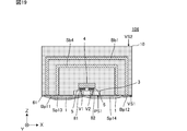
- FIG. 1 is a perspective view of a wireless IC device 101 according to the first embodiment.
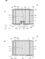
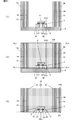
- 2A is a plan view of the wireless IC device 101
- FIG. 2B is a right side view of the wireless IC device 101
- FIG. 2C is a bottom view of the wireless IC device 101.
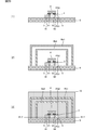
- 3A is a cross-sectional view of the wireless IC device 101
- FIG. 3B is a cross-sectional view of a different part of the wireless IC device 101.
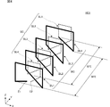
- FIG. 4 is a perspective view schematically showing each conductor portion of the helical coil HC1 included in the wireless IC device 101. As shown in FIG. FIG. FIG.
- FIG. 5A is a perspective view schematically showing a conductor portion of a large-diameter loop provided in the helical coil HC1
- FIG. 5B is a schematic diagram showing a conductor portion of a small-diameter loop provided in the helical coil HC1.
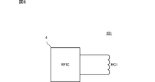
- FIG. 6 is a circuit diagram of the wireless IC device 101.
- FIG. 7A is an enlarged view of the DP1 portion in FIG. 2A
- FIG. 7B is a detailed cross-sectional view along the line AA in FIG. 7A.
- FIG. 8 is a cross-sectional view illustrating the manufacturing process of the wireless IC device 101 in order.
- FIG. 8 is a cross-sectional view illustrating the manufacturing process of the wireless IC device 101 in order.
- FIG. 9 is a cross-sectional view sequentially illustrating the manufacturing process of the wireless IC device 101.
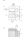
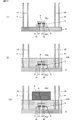
- FIG. 10A is a cross-sectional view of the wireless IC device 102 according to the second embodiment
- FIG. 10B is a cross-sectional view of the wireless IC device 102 taken along line BB in FIG. 10A. is there.
- FIG. 11 is a cross-sectional view illustrating a part of the manufacturing process of the wireless IC device 102 in order.
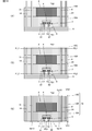
- FIG. 12 is a cross-sectional view of the wireless IC device 103 according to the third embodiment.
- FIG. 13 is a cross-sectional view illustrating the manufacturing process of the wireless IC device 103 in order.
- FIG. 14 is a cross-sectional view sequentially illustrating the manufacturing process of the wireless IC device 103.
- FIG. 15 is a cross-sectional view sequentially illustrating the manufacturing process of the wireless IC device 103.
- FIG. 16 is a cross-sectional view of the wireless IC device 104 according to the fourth embodiment.
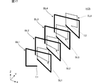
- FIG. 17 is a perspective view schematically showing each conductor portion of the helical coil HC5 according to the fifth embodiment.
- FIG. 18A is a perspective view schematically showing a conductor portion of a large-diameter loop provided in the helical coil HC5, and
- FIG. 18B schematically shows a conductor portion of a small-diameter loop provided in the helical coil HC5.
- FIG. 19 is a cross-sectional view of the wireless IC device 106 according to the sixth embodiment.
- FIG. 20 is a cross-sectional view sequentially illustrating the manufacturing process of the wireless IC device 106.
- FIG. 21 is a cross-sectional view sequentially illustrating the manufacturing process of the wireless IC device 106.
- FIG. 22 is a cross-sectional view of the wireless IC device 107 according to the seventh embodiment.
- the helical coils according to some embodiments described below are coil antennas that can be used in, for example, the HF band, the LF band, the UHF band, the SHF band, and the like as magnetic flux radiating elements.
- the helical coil can also be used as an inductor element. Therefore, unless otherwise specified, helical coils according to some embodiments described below are examples of both a coil antenna and an inductor element.
- wireless IC devices according to some embodiments described below include an RFIC, a resin main body, and a helical coil, and are, for example, RFID communication devices such as chip-like RFID tags provided on articles to be managed. .
- the article to which the RFID tag is attached is, for example, portable information terminals such as toys and mobile phones, building materials such as scaffolding materials, and industrial materials such as gas cylinders.
- FIG. 1 is a perspective view of a wireless IC device 101 according to the first embodiment.
- 2A is a plan view of the wireless IC device 101
- FIG. 2B is a right side view of the wireless IC device 101
- FIG. 2C is a bottom view of the wireless IC device 101.
- 3A is a cross-sectional view of the wireless IC device 101
- FIG. 3B is a cross-sectional view of a different part of the wireless IC device 101.
- the first insulating layer 1 and the second insulating layer 2 are hatched for easy understanding of the structure.
- 3A and 3B some thicknesses are exaggerated. The same applies to the sectional views in the following embodiments.
- the protective layer 62 is not shown for easy understanding of the structure.
- the wireless IC device 101 has a rectangular parallelepiped shape whose longitudinal direction coincides with the X-axis direction, and includes a resin main body 10, a helical coil (described in detail later), a first insulating layer 1, a second insulating layer 2, a wiring board 3, An RFIC 4 and protective layers 61 and 62 are provided.
- the resin body 10 has a rectangular parallelepiped shape whose longitudinal direction coincides with the X-axis direction, and has a first surface VS1 and a second surface VS2 facing the first surface VS1.
- the resin body 10 is a thermosetting resin such as an epoxy resin.
- FIG. 4 is a perspective view schematically showing each conductor portion of the helical coil HC1 included in the wireless IC device 101.
- FIG. FIG. 5A is a perspective view schematically showing a conductor portion of a large-diameter loop provided in the helical coil HC1
- FIG. 5B is a schematic diagram showing a conductor portion of a small-diameter loop provided in the helical coil HC1. It is the perspective view shown in. In FIG. 4, the small-diameter loop is shown by a broken line in order to make the structure of the helical coil HC1 easy to understand.
- the helical coil HC1 has a winding axis AX along the first surface VS1 of the resin body 10, and includes a plurality of large diameter loops BL1, BL2, BL3, BL4 and a plurality of small diameter loops SL1, SL2, SL3, SL4.
- the helical coil HC1 has a first portion (described in detail later) embedded in the resin body 10 and a second portion (described in detail later) patterned on the surface of the resin body 10.
- the winding axis AX of the helical coil HC1 according to the present embodiment is parallel to the Y-axis direction.
- the plurality of small-diameter loops SL1, SL2, SL3, SL4 are large-diameter loops BL1, BL2, BL3, as viewed from the Y-axis direction (corresponding to the “winding axis direction” in the present invention) as will be described in detail later. It is arranged inside the outer diameter of BL4.
- each of the small-diameter loops SL1, SL2, SL3, SL4 has substantially the same shape, and is perpendicular to the first surface VS1 of the resin body 10.
- the plurality of small-diameter loops SL1, SL2, SL3, SL4 include first small-diameter columnar conductors 11, 12, 13, 14, second small-diameter columnar conductors 21, 22, 23, 24, first small-diameter conductor patterns Sp11, Sp12, Sp13, Sp14 and second small-diameter conductor patterns Sp21, Sp22, Sp23, Sp24 are included.
- the small-diameter loop SL1 includes a first small-diameter columnar conductor 11, a second small-diameter columnar conductor, a first small-diameter conductor pattern Sp11, and a second small-diameter conductor pattern Sp21.
- the small-diameter loop SL2 includes a first small-diameter columnar conductor 12, a second small-diameter columnar conductor 22, a first small-diameter conductor pattern Sp12, and a second small-diameter conductor pattern Sp22.
- the small-diameter loop SL3 includes a first small-diameter columnar conductor 13, a second small-diameter columnar conductor 23, a first small-diameter conductor pattern Sp13, and a second small-diameter conductor pattern Sp23.
- the small-diameter loop SL4 includes a first small-diameter columnar conductor 14, a second small-diameter columnar conductor, a first small-diameter conductor pattern Sp14, and a second small-diameter conductor pattern Sp24.
- the first small-diameter columnar conductors 11, 12, 13, and 14 and the second small-diameter columnar conductors 21, 22, 23, and 24 are in the Z-axis direction (corresponding to the “direction perpendicular to the first surface” of the resin body in the present invention). And a columnar metal body arranged in the Y-axis direction.
- the first small-diameter columnar conductors 11, 12, 13, 14 and the second small-diameter columnar conductors 21, 22, 23, 24 are embedded in the resin body 10 except for the first and second ends.
- Each of the first small-diameter columnar conductors 11, 12, 13, 14 and the second small-diameter columnar conductors 21, 22, 23, and 24 is, for example, a cylindrical Cu pin.
- a Cu wire having a circular cross section is a predetermined length unit. It is obtained by cutting with.
- the cross-sectional shape may be a rectangle or a polygon.
- the first small-diameter columnar conductors 11, 12, 13, 14 and the second small-diameter columnar conductors 21, 22, 23, 24 are “first portions” of the helical coil HC 1 embedded in the resin body 10. It corresponds to.
- the first small-diameter conductor patterns Sp11, Sp12, Sp13, Sp14 are conductor patterns formed on the first surface VS1 of the resin main body 10 as shown in FIGS. 2A and 2B, and are columnar conductors ( The first small diameter columnar conductor or the second small diameter columnar conductor) is connected to the first end.
- the first small-diameter conductor pattern Sp11 connects the first end of the first small-diameter columnar conductor 12 and the first end of the second small-diameter columnar conductor 21.
- the first small-diameter conductor pattern Sp12 connects the first end of the first small-diameter columnar conductor 13 and the first end of the second small-diameter columnar conductor 22.
- the first small-diameter conductor pattern Sp13 connects the first end of the first small-diameter columnar conductor 14 and the first end of the second small-diameter columnar conductor 23.
- the first small-diameter conductor pattern Sp14 connects the first end of the second small-diameter columnar conductor 24 and the RFIC.
- the first small-diameter conductor patterns Sp11, Sp12, Sp13, and Sp14 are obtained by coating a conductor film formed by printing Ag paste, for example, with a plating film such as Cu.
- 2nd small diameter conductor pattern Sp21, Sp22, Sp23, Sp24 is a conductor pattern formed in the 2nd surface VS2 of the resin main body 10, as shown to FIG. 2 (A) and FIG. 2 (B), and columnar conductor ( The first small-diameter columnar conductor and the second small-diameter columnar conductor are connected to the second end.
- the second small-diameter conductor pattern Sp ⁇ b> 21 connects the second end of the first small-diameter columnar conductor 11 and the second end of the second small-diameter columnar conductor 21.
- the second small-diameter conductor pattern Sp ⁇ b> 22 connects between the second end of the first small-diameter columnar conductor 12 and the second end of the second small-diameter columnar conductor 22.
- the second small-diameter conductor pattern Sp ⁇ b> 23 connects between the second end of the first small-diameter columnar conductor 13 and the second end of the second small-diameter columnar conductor 23.
- the second small-diameter conductor pattern Sp ⁇ b> 24 connects the second end of the first small-diameter columnar conductor 14 and the second end of the second small-diameter columnar conductor 24.
- the second small-diameter conductor patterns Sp21, Sp22, Sp23, Sp24 are, for example, obtained by coating a conductor pattern formed by printing Ag paste with a plating film such as Cu.
- the first small-diameter conductor patterns Sp11, Sp12, Sp13, Sp14 and the second small-diameter conductor patterns Sp21, Sp22, Sp23, Sp24 are “second” of the helical coil HC1 patterned on the surface of the resin body 10. Corresponds to “part”.
- the first insulating layer 1 is formed on the surface of the first surface VS1 of the resin body 10 and the first small-diameter conductor patterns Sp11, Sp12, Sp13, Sp14.
- the first insulating layer 1 is an insulator film that covers at least a part of the surface of the first small-diameter conductor pattern Sp11, Sp12, Sp13, Sp14. In the present embodiment, as shown in FIGS. 2A, 2B, 3C, etc., the first insulating layer 1 covers the entire first small-diameter conductor patterns Sp11, Sp12, Sp13, Sp14. .
- the first insulating layer 1 is a thermosetting resin such as an epoxy resin.
- the first insulating layer 1 is sandwiched between the portions overlapping with (described later in detail).
- the second insulating layer 2 is formed on the surface of the second surface VS2 of the resin main body 10 and the second small-diameter conductor patterns Sp21, Sp22, Sp23, Sp24.
- the second insulating layer 2 is an insulating film that covers at least part of the surface of the second small-diameter conductor pattern Sp21, Sp22, Sp23, Sp24. In the present embodiment, as shown in FIGS. 2A, 2B, 3A, etc., the second insulating layer 2 covers the entire second small-diameter conductor patterns Sp21, Sp22, Sp23, Sp24. .
- the second insulating layer 2 is a thermosetting resin such as an epoxy resin.
- the second small-diameter conductor patterns Sp21, Sp22, Sp23, Sp24 and the second large-diameter conductor patterns Bp21, Bp22, Bp23, Bp24 are sandwiched between the portions overlapping with (described later in detail).
- each of the large-diameter loops BL1, BL2, BL3, BL4 has substantially the same shape and is perpendicular to the first surface VS1 of the resin body 10.
- the plurality of large-diameter loops BL1, BL2, BL3, BL4 include first large-diameter columnar conductors 31, 32, 33, 34, second large-diameter columnar conductors 41, 42, 43, 44, first large-diameter conductor patterns Bp11, Bp12, Bp13, Bp14, Bp15 and second large-diameter conductor patterns Bp21, Bp22, Bp23, Bp24.
- the large diameter loop BL1 includes a first large diameter columnar conductor 31, a second large diameter columnar conductor 41, a first large diameter conductor pattern Bp11, and a second large diameter conductor pattern Bp21.
- the large diameter loop BL2 includes a first large diameter columnar conductor 32, a second large diameter columnar conductor 42, a first large diameter conductor pattern Bp12, and a second large diameter conductor pattern Bp22.
- the large-diameter loop BL3 includes a first large-diameter columnar conductor 33, a second large-diameter columnar conductor 43, a first large-diameter conductor pattern Bp13, and a second large-diameter conductor pattern Bp23.
- the large-diameter loop BL4 includes a first large-diameter columnar conductor 34, a second large-diameter columnar conductor 44, first large-diameter conductor patterns Bp14 and Bp15, and a second large-diameter conductor pattern Bp24.
- the first large-diameter columnar conductors 31, 32, 33, 34 and the second large-diameter columnar conductors 41, 42, 43, 44 are columnar metal bodies that extend in the Z-axis direction and are arranged in the Y-axis direction. is there.
- the first large-diameter columnar conductors 31, 32, 33, and 34 and the second large-diameter columnar conductors 41, 42, 43, and 44 are embedded in the resin body 10 except for the first and second ends.
- Each of the first large-diameter columnar conductors 31, 32, 33, and 34 and the second large-diameter columnar conductors 41, 42, 43, and 44 is, for example, a cylindrical Cu pin. Obtained by cutting in long units.
- the cross-sectional shape may be a rectangle or a polygon.
- the first large-diameter columnar conductors 31, 32, 33, 34 and the second large-diameter columnar conductors 41, 42, 43, 44 are “first” of the helical coil HC 1 embedded in the resin body 10. Corresponds to “part”.
- the first large-diameter conductor patterns Bp11, Bp12, Bp13, Bp14, and Bp15 are formed on the first surface VS1 of the resin body 10 and the surface of the first insulating layer 1 as shown in FIGS. 2 (A) and 2 (B). It is a conductor pattern formed over and connected to the columnar conductor (first large diameter columnar conductor or second large diameter columnar conductor) first end.
- the first large-diameter conductor pattern Bp11 connects the RFIC and the first end of the first large-diameter columnar conductor 31.
- the first large-diameter conductor pattern Bp12 connects the first end of the first large-diameter columnar conductor 32 and the first end of the second large-diameter columnar conductor 41.
- the first large-diameter conductor pattern Bp13 connects the first end of the first large-diameter columnar conductor 33 and the first end of the second large-diameter columnar conductor 42.
- the first large-diameter conductor pattern Bp14 connects the first end of the first large-diameter columnar conductor 34 and the first end of the second large-diameter columnar conductor 43.
- the first large-diameter conductor pattern Bp15 connects the first end of the second large-diameter columnar conductor and the first end of the first small-diameter columnar conductor 11 described above.
- the first large-diameter conductor patterns Bp11, Bp12, Bp13, Bp14, and Bp15 are obtained by coating a conductor pattern formed by printing Ag paste, for example, with a plating film such as Cu.
- the second large-diameter conductor patterns Bp21, Bp22, Bp23, Bp24 are formed across the second surface VS2 and the second insulating layer 2 of the resin body 10, as shown in FIGS. 2 (A) and 2 (B).
- the conductor pattern is connected to the second end of the columnar conductor (the first large-diameter columnar conductor and the second large-diameter columnar conductor).
- the second large-diameter conductor pattern Bp21 connects between the second end of the first large-diameter columnar conductor 31 and the second end of the second large-diameter columnar conductor 41.
- the second large-diameter conductor pattern Bp22 connects the second end of the first large-diameter columnar conductor 32 and the second end of the second large-diameter columnar conductor 42.
- the second large-diameter conductor pattern Bp23 connects the second end of the first large-diameter columnar conductor 33 and the second end of the second large-diameter columnar conductor 43.
- the second large diameter conductor pattern Bp24 connects between the second end of the first large diameter columnar conductor 34 and the second end of the second large diameter columnar conductor 44.
- the second large-diameter conductor patterns Bp21, Bp22, Bp23, and Bp24 are obtained by coating a conductor film formed by printing Ag paste, for example, with a plating film such as Cu.
- the helical coil HC1 in which the first large conductor patterns Bp11, Bp12, Bp13, Bp14, Bp15 and the second large conductor patterns Bp21, Bp22, Bp23, Bp24 are patterned on the surface of the resin body 10. This corresponds to the “second part”.
- the outer diameter dimensions of these small diameter loops SL1, SL2, SL3, SL4 are smaller than the outer diameter dimensions of the large diameter loops BL1, BL2, BL3, BL4 when viewed from the Y-axis direction. Further, the inner diameter dimensions of the small diameter loops SL1, SL2, SL3, SL4 are smaller than the inner diameter dimensions of the large diameter loops BL1, BL2, BL3, BL4 when viewed from the Y-axis direction. And small diameter loop SL1, SL2, SL3, SL4 is arrange
- the small-diameter loops SL1, SL2, SL3, and SL4 are arranged inside the inner diameters of the large-diameter loops BL1, BL2, BL3, and BL4 when viewed from the Y-axis direction.
- the plurality of large-diameter loops BL1, BL2, BL3, BL4 are connected to each other to form a helical large-diameter coil BC of about 4 turns, and the plurality of small-diameter loops SL1, SL2, SL3, SL4 are connected to each other.
- a helical small-diameter SC having about 4 turns is formed.
- the second end Be2 of the large diameter coil BC is connected to the first end Se1 of the small diameter coil SC to constitute the helical coil HC1.
- the extending direction (+ Y direction) from the first end Be1 to the second end Be2 of the large-diameter coil BC in the Y-axis direction is the second from the first end Se1 of the small-diameter coil SC in the Y-axis direction.
- the direction opposite to the extending direction ( ⁇ Y direction) toward the end Se2 is opposite.
- at least a part of the large-diameter loop formation region BFE in the Y-axis direction overlaps the small-diameter loop formation region SFE in the Y-axis direction.
- a plurality of second large-diameter conductor patterns Bp21, Bp22, Bp23, Bp24 and a plurality of second small-diameter conductor patterns Sp21, Sp22, Sp23, Sp24 are represented by Y They are arranged alternately one after another in the axial direction.
- the large-diameter loop and the small-diameter loop are arranged without gaps along the Y-axis direction when viewed from the Z-axis direction (corresponding to “viewing the second surface of the resin main body of the present invention in plan view”).
- the plurality of second small diameter columnar conductors 21, 22, 23, 24 and the plurality of second large diameter columnar conductors 41, 42, 43, 44 are Y They are alternately arranged with respect to the axial direction.
- the plurality of first small-diameter columnar conductors 11, 12, 13, 14 and the plurality of first large-diameter columnar conductors 31, 32, 33, 34 are alternately arranged in the Y-axis direction. Is done.
- the large-diameter loop and the small-diameter loop are along the Y-axis direction when viewed from the X-axis direction (corresponding to the “direction parallel to the first surface and the direction perpendicular to the winding axis direction” in the present invention). Are arranged without gaps.
- the wiring board 3 is a flat plate having a first main surface PS1 and a second main surface PS2 facing the first main surface PS1 and having a rectangular planar shape.
- the wiring board 3 includes mounting electrodes 81 and 82, interlayer connection conductors V1 and V2, and the like.
- the mounting electrodes 81 and 82 are electrodes for mounting the RFIC 4, and are formed on the second main surface PS2 of the wiring board 3.
- the wiring board 3 is a thermosetting printed wiring board such as an epoxy resin, and is typically a double-sided through-hole board.
- the wiring board 3 is not limited to this, and may be a printed wiring board or a ceramic substrate whose base material is a thermoplastic resin such as polyimide resin.
- the wiring board 3 may be a single layer substrate or a multilayer substrate.
- the wiring board 3 is arranged such that the second main surface PS2 is embedded inside the resin body 10 and the first main surface PS1 is exposed from the resin body 10.
- the wiring board 3 is embedded in the resin main body 10 such that the first main surface PS1 of the wiring board 3 and the first surface VS1 of the resin main body 10 are on the same plane.
- the first main surface PS1 and the second main surface PS2 of the wiring board 3 are disposed so as to be parallel to the X-axis direction and the Y-axis direction. That is, the first main surface PS1 and the second main surface PS2 are arranged so as to be parallel to the winding axis of the helical coil HC1.
- the wiring board 3 is disposed inside the large-diameter loops BL1, BL2, BL3, BL4 and the small-diameter loops SL1, SL2, SL3, SL4 as viewed from the Y-axis direction.
- the RFIC 4 is mounted on the second main surface PS2 of the wiring board 3 and embedded in the resin main body 10 as shown in FIGS. 1 and 2A.
- the antenna port of the RFIC 4 is connected to mounting electrodes 81 and 82 formed on the second main surface PS2 of the wiring board 3, respectively.
- the mounting electrodes 81 and 82 are connected to the first end E1 and the second end E2 of the helical coil HC1 shown in FIG. 4 via the interlayer connection conductors V1 and V2, respectively. That is, the RFIC 4 is connected to the first end and the second end of the helical coil HC1, respectively.
- the RFIC 4 is, for example, a packaged RFIC.
- the RFIC 4 may be a bare chip RFIC chip.
- the RFIC chip and the mounting electrodes 81 and 82 (land pattern) may be connected by a wire.
- the protective layers 61 and 62 are formed on the first surface VS ⁇ b> 1 and the second surface VS ⁇ b> 2 of the resin main body 10, and are provided with a conductor pattern (first large diameter conductor pattern, second large diameter conductor pattern, first small diameter conductor pattern, second small diameter). The formation surface of the conductor pattern is covered.
- the protective layers 61 and 62 are resin films provided for the purpose of preventing oxidation of the conductor pattern, improving heat resistance, and preventing short-circuiting between conductors due to metal foreign matter, and are, for example, solder resist films.
- the protective layers 61 and 62 are not essential.
- FIG. 6 is a circuit diagram of the wireless IC device 101.
- the wireless IC device 101 includes, for example, an HF band RFIC for an HF band RFID system.
- the helical coil HC1 is connected to the RFIC 4, and an LC resonance circuit is configured by the helical coil HC1 and the capacitive component of the RFIC 4. Its resonant frequency is substantially equal to the communication frequency of the RFID system.
- the communication frequency band is, for example, the 13.56 MHz band.
- the “wireless IC device” may be composed of a helical coil HC1 and an RFIC chip, or an integrated module in which an RFIC chip is mounted on a substrate provided with a helical coil HC1 and a matching circuit. And may be configured.
- An “RFID tag” includes an RFIC and a helical coil connected to the RFIC, and is an information medium that reads and writes data in a built-in memory in a non-contact manner using radio waves (electromagnetic waves) or magnetic fields. It is defined as That is, the wireless IC device of this embodiment is configured as an RFID tag.
- FIG. 7A is an enlarged view of the DP1 portion in FIG. 2A
- FIG. 7B is a detailed cross-sectional view along the line AA in FIG. 7A. 7A and 7B, the protective layer 62 is not shown for easy understanding of the structure.
- the large-diameter conductor pattern and the small-diameter conductor pattern include a base electrode layer formed on the surface of the resin body 10 and a plating electrode layer laminated on the base electrode layer.
- the second large-diameter conductor pattern Bp21 shown in FIG. 7A will be described as an example.
- the second large-diameter conductor pattern Bp21 includes a base electrode layer BA1 and a plating electrode layer BC1, and the base electrode layer BA1 is an end.
- the line width of the portion is smaller than the diameter of the upper end surface of the second large-diameter columnar conductor 41.
- the end portion of the base electrode layer BA1 is formed so as to cover a part of the upper end surface of the second large-diameter columnar conductor 41.
- the plating electrode layer BC1 is formed so as to cover the upper end surface of the second large-diameter columnar conductor 41 that is not covered with the base electrode layer BA1 and the base electrode layer BA1.
- the base electrode layer is formed by screen printing a conductive paste such as Ag.
- a plating electrode layer is a plating film which coat
- the large-diameter conductor pattern and the small-diameter conductor pattern can all be made thicker by forming a Cu plating film. Therefore, the DCR of the helical coil can be further reduced.
- the columnar conductor is a Cu pin
- the plated electrode layer which is a Cu plating film, covers not only the base electrode layer but also the upper end surface of the columnar conductor not covered by the base electrode layer. It is formed. Therefore, with this configuration, the bonding strength of the large-diameter conductor pattern and the small-diameter conductor pattern and the columnar conductor is greater than when the base electrode layer, which is an Ag conductor pattern, is coated on the entire upper end surface of the columnar conductor that is a Cu pin. Can be high.
- the wireless IC device 101 according to the present embodiment has the following effects.
- (A) In the present embodiment, at least a portion where the small diameter conductor pattern (first small diameter conductor pattern, second small diameter conductor pattern) and the large diameter conductor pattern (first large diameter conductor pattern, second large diameter conductor pattern) overlap. Insulating layers (first insulating layer, second insulating layer) are sandwiched. In this configuration, the small-diameter conductor pattern and the large-diameter conductor pattern are not formed on the same plane, and an insulating layer is interposed between the small-diameter conductor pattern and the large-diameter conductor pattern. The possibility of contact with the conductor pattern (short circuit between lines) is low.
- the large-diameter conductor pattern and the small-diameter conductor pattern are ensured without separately providing a connection member such as a jumper chip. Therefore, the large-diameter loop and the small-diameter loop can be arranged at a narrow pitch in the Y-axis direction, and it becomes easy to obtain a helical coil having a desired number of turns and a desired inductance value.
- the small-diameter conductor pattern and the large-diameter conductor pattern partially overlap each other when viewed from the Z-axis direction, so that the line width of the small-diameter conductor pattern and the large-diameter conductor pattern can be easily increased, and the helical coil HC1 DCR can be further reduced.
- the large-diameter loops BL1, BL2, BL3, and BL4 and the small-diameter loops SL1, SL2, SL3, and SL4 constituting the helical coil HC1 are formed of columnar conductors. . Therefore, the DCR of the large-diameter loop and the small-diameter loop can be reduced as compared with the case where the sintered metal body is formed by firing the conductive paste, or the thin-film metal body is formed by etching the conductive thin film. A lossy helical coil is obtained. Further, since the resistance of the entire helical coil can be reduced, a highly sensitive wireless IC device or a small wireless IC device for high sensitivity can be obtained.
- the radial columnar conductors are arranged in the Y-axis direction and arranged in a staggered manner as viewed from the Z-axis direction.
- insulation between adjacent large-diameter conductor patterns and small-diameter conductor patterns is ensured without separately providing a connection member such as a jumper chip. Therefore, the large diameter loop and the small diameter loop can be arranged at a narrow pitch in the Y-axis direction.
- a large-diameter conductor pattern (first large-diameter conductor pattern and second large-diameter conductor pattern) and a small-diameter conductor pattern (first) used for a part of the large-diameter loop and a part of the small-diameter loop.
- the small-diameter conductor pattern and the second small-diameter conductor pattern are conductor patterns formed on the surface of the resin body 10 and the like, not wires or the like.
- the possibility of contact (short between lines) between adjacent large-diameter conductor patterns or between adjacent small-diameter conductor patterns is low, so the gap between large-diameter conductor patterns arranged in the Y-axis direction can be easily reduced.
- the gap between the small-diameter conductor patterns arranged in the Y-axis direction can be easily reduced.
- the desired number of turns and the desired inductance value can be obtained even if the occupation area (dimension in the Y-axis direction) is the same. It becomes easy to obtain the helical coil which has.
- the mounting electrode 81 of the RFIC 4 , 82 (land pattern) or the like hardly interferes with the formation of the magnetic field of the helical coil HC1. Further, the adverse effect (malfunction, unstable operation, etc.) on the RFIC 4 due to the magnetic field of the helical coil HC1 is small. Furthermore, the adverse effect on the helical coil due to noise generated from the digital circuit section of the RFIC 4 (decrease in reception sensitivity, wraparound of the transmission signal to the reception circuit, etc.) is small.
- the RFIC 4 is arranged inside the helical coil. Therefore, the protection function of the RFIC 4 is high. Further, since the RFIC 4 is not exposed to the outside of the wireless IC device 101, an increase in size due to mounting the RFIC 4 outside the helical coil can be avoided.
- the wireless IC device 101 includes a surface-mounted component such as the RFIC 4, a part of the large-diameter loop (first large-diameter columnar conductor, second large-diameter columnar conductor), and a part of the small-diameter loop (first small-diameter columnar conductor, Since the second small-diameter columnar conductor) is protected by the resin body 10, the entire wireless IC device is robust.
- the wireless IC device is embedded in a resin molded article, the solder connection portion of the surface mount chip component is protected against a high temperature resin (for example, a high temperature resin of 300 ° C. or higher) that flows during injection molding.
- a high temperature resin for example, a high temperature resin of 300 ° C. or higher
- the RFIC 4 includes the large-diameter loops BL1, BL2, BL3, BL4, the small-diameter loops SL1, SL2, SL3, SL4, the first large-diameter conductor patterns Bp11, Bp12, Bp13, Bp14, Bp15, Two large-diameter conductor patterns Bp21, Bp22, Bp23, Bp24, the first small-diameter conductor patterns Sp11, Sp12, Sp13, Sp14 and the second small-diameter conductor patterns Sp21, Sp22, Sp23, Sp24, and the like, and Surrounded by the resin body 10 and the wiring board 3.
- the resin body 10 and the wiring board 3 are bonded together by joining the resins, and the surface-mounted components and small-diameter loops do not come off or deform, so after cooling The soldered joint will return to normal. Therefore, the inductance value of the helical coil can be maintained.
- the wireless IC device 101 has a large-diameter conductor pattern constituting a large-diameter loop (first large-diameter conductor patterns Bp11, Bp12, Bp13, Bp14, Bp15 and second large-diameter conductor patterns Bp21, Bp22, Bp23, Bp24). Is formed over the surface of the resin body 10 and the surfaces of the insulating layers (the first insulating layer 1 and the second insulating layer 2). Therefore, the substantial opening diameter of the helical coil HC1 is large.
- a helical coil (coil antenna) having a size substantially equal to the size of the chip-shaped wireless IC device 101 can be configured, and a large communication distance is ensured despite being a small chip-shaped component.
- communication can be performed with a relatively wide positional relationship with respect to the antenna of the communication partner.
- the first small-diameter conductor patterns Sp11, Sp12, Sp13, Sp14 and the second small-diameter conductor patterns Sp21, Sp22, Sp23, Sp24 are formed on the surface of the resin body 10 by patterning. Therefore, the connection between the first ends of the first small-diameter columnar conductors 11, 12, 13, 14 and the first ends of the second small-diameter columnar conductors 21, 22, 23, 24, and the first small-diameter columnar conductors 11, 12, 13 , 14 and the second ends of the second small-diameter columnar conductors 21, 22, 23, 24 are facilitated.
- the first large-diameter conductor patterns Bp11, Bp12, Bp13, Bp14, Bp15, and the second large-diameter conductor pattern Bp21, over the surface of the resin main body 10 and the surface of the insulating layer, are patterned.
- Bp22, Bp23, and Bp24 are formed.
- connection between the second ends of 32, 33, and 34 and the second ends of the second large-diameter columnar conductors 41, 42, 43, and 44 is facilitated.
- the first large-diameter conductor pattern Bp11, Bp12, Bp13, Bp14, Bp15, the second large-diameter conductor pattern Bp21, Bp22, Bp23, extending in the X-axis direction, Bp24, the first small-diameter conductor patterns Sp11, Sp12, Sp13, Sp14 and the second small-diameter conductor patterns Sp21, Sp22, Sp23, Sp24 can all be made thick by forming a plating film of Cu or the like. Therefore, the DCR of the helical coil can be further reduced.
- the extending direction (+ Y direction) from the first end Be1 to the second end Be2 of the large-diameter coil BC in the Y-axis direction is the same as that of the small-diameter coil SC in the Y-axis direction.
- the extending direction ( ⁇ Y direction) from the first end Se1 to the second end Se2 is opposite to the extending direction.
- at least a part of the large-diameter loop formation region BFE in the Y-axis direction overlaps the small-diameter loop formation region SFE in the Y-axis direction.
- a helical coil having a small occupied area (particularly the dimension in the Y-axis direction) relative to the number of turns can be realized. Also, with this configuration, the conductor that does not contribute to inductance can be shortened, so that the DCR of the helical coil can be further reduced.
- the wireless IC device 101 has a structure in which the wiring board 3 is embedded in the resin main body 10 so that the first main surface PS1 of the wiring board 3 and the first surface VS1 of the resin main body 10 are on the same plane.
- the first small-diameter conductor pattern, the first large-diameter conductor pattern, and the like formed over the first surface VS1 and the first main surface PS1 can be easily formed by patterning, the first end of the helical coil HC1 And the connection between the second end and the RFIC 4 is facilitated.
- the large-diameter loops BL1, BL2, BL3, and BL4 and the small-diameter loops SL1, SL2, SL3, and SL4 are arranged without gaps along the Y-axis direction when viewed from the Z-axis direction.
- the magnetic flux generated in the helical coil is difficult to leak from the gap between the large-diameter loop and the small-diameter loop that are adjacent to each other. Therefore, a helical coil having a high inductance value can be configured.
- magnetic field coupling can be performed with a relatively wide positional relationship with respect to the coil antenna on the communication partner side.
- the edge in the Y-axis direction of the large-diameter loop and the edge in the Y-axis direction of the small-diameter loop are viewed from the Z-axis direction.
- the end portion preferably overlaps partly (see FIG. 2A).
- the large-diameter loops BL1, BL2, BL3, and BL4 and the small-diameter loops SL1, SL2, SL3, and SL4 are arranged without gaps along the Y-axis direction when viewed from the X-axis direction. Yes.
- this configuration makes it possible to configure a helical coil having a high inductance value. Further, when a helical coil is used as a coil antenna, magnetic field coupling can be performed with a relatively wide positional relationship with respect to the coil antenna on the communication partner side.
- the edge in the Y-axis direction of the large-diameter loop and the edge in the Y-axis direction of the small-diameter loop are viewed from the X-axis direction.
- the end portion preferably overlaps partly (see FIG. 2B).
- the helical coil HC1 including the large-diameter coil BC of about 4 turns and the small-diameter coil SC of about 4 turns is shown, but the present invention is not limited to this.
- the number of turns of the large-diameter coil BC and the number of turns of the small-diameter coil can be appropriately changed as long as they are larger than one.
- the configuration in which one large-diameter coil BC and one small-diameter coil SC are connected is shown, but the present invention is not limited to this.
- a plurality of large-diameter coils and a plurality of small-diameter coils may be alternately and sequentially connected.
- the number of large diameter coils and the number of small diameter coils do not need to be the same number.
- the plurality of large-diameter coils may have different numbers of turns, and the plurality of small-diameter coils may have different numbers of turns.
- the wiring board 3 on which the RFIC 4 is mounted is prepared. Specifically, mounting electrodes 81 and 82 (for mounting the RFIC 4 on the second main surface PS2 of the wiring board 3 having the first main surface PS1 and the second main surface PS2 opposed to the first main surface PS1. Land pattern) or the like. Further, in the thickness direction of the wiring board 3, interlayer connection conductors V 1 and V 2 formed inside the wiring board 3 and connected to the mounting electrodes 81 and 82 are formed.
- the conductive bonding material 5 such as a solder paste is formed on the mounting electrodes 81 and 82 for mounting the RFIC 4. At this time, the conductor pattern is not formed on the first main surface PS1 side of the wiring board 3.
- the wiring board 3 is a printed wiring board based on a thermosetting resin such as a glass epoxy board or an epoxy resin, for example, but a thick film pattern is formed on a board or ceramic board based on a thermoplastic resin such as a polyimide resin. May be formed.
- the wiring board 3 may be a single layer substrate or a multilayer substrate.
- the mounting electrodes 81 and 82 are formed by patterning a metal foil having a small specific resistance, such as Cu or Ag.
- the mounting electrodes 81 and 82 are formed by patterning a plating film on the second main surface PS2 of the wiring board 3, or patterning a conductor paste. It may be what you did.
- the mounting electrodes 81 and 82 have a cross-sectional dimension of 18 ⁇ m ⁇ 100 ⁇ m. After performing these patterning, it is preferable that the total film thickness is increased to 40 to 50 ⁇ m by plating with Cu or the like.
- the interlayer connection conductors V1 and V2 are through holes in which a plating film is provided on the inner wall of a through hole that penetrates the wiring board 3, for example.
- the RFIC 4 is mounted on the second main surface PS2 of the wiring board 3 via the conductive bonding material 5 such as solder. Specifically, after mounting components such as RFIC4 on the second main surface PS2 of the wiring board 3 with a mounter, these components are soldered by a reflow process. By this step, the RFIC 4 is electrically connected to the wiring board 3 and is structurally bonded.
- RFIC4 is a packaged RFIC for RFID tags. Further, the RFIC 4 may be a bare chip RFIC chip.
- a support base 6 having an adhesive layer on the main surface is prepared, and the wiring board 3 on which the RFIC 4 is mounted is mounted on the support base 6.
- the first main surface PS1 side of the wiring board 3 is fixed to the support layer 6 with the adhesive layer side.
- the adhesive layer included in the support base 6 is, for example, an adhesive resin.
- This process of mounting the RFIC 4 on the support base 6 is an example of the “first process” in the present invention.
- the first end sides of the columnar conductors (the first small-diameter columnar conductor 14 and the like, the second small-diameter columnar conductor 24 and the like, the first large-diameter columnar conductor 31 and the second large-diameter columnar conductor 41 and the like)
- the support base 6 is fixed to stand on the adhesive layer side.
- each columnar conductor is mounted in a state in which the first end side of each columnar conductor is firmly fixed to the support base 6 via the adhesive layer.
- Each columnar conductor is a columnar post made of Cu.
- the columnar conductors are not limited to those containing Cu as the main component, but those containing Cu as the main component are preferable in terms of conductivity and workability.
- This step of standing the first end of each of the first small-diameter columnar conductor, the second small-diameter columnar conductor, the first large-diameter columnar conductor, and the second large-diameter columnar conductor on the support base 6 is the “second step in the present invention. Is an example.
- a resin body 10 is formed (coated with resin). Specifically, the resin body 10 coated with epoxy resin or the like at a predetermined height (at least the height of the columnar conductor) on the support base 6 is ground together with the columnar conductor as shown in (4) of FIG. The second end of the columnar conductor is exposed from the second surface VS2 of the resin main body 10 by planarly grinding (or cutting or polishing) the line PL1.
- an epoxy resin or the like is applied to a predetermined height (below the height of the columnar conductor), and then the resin main body 10 is ground (or cut or polished) together with the columnar conductor in a second manner.
- the second end of the columnar conductor may be exposed on the surface VS2.
- the resin main body 10 may be provided by applying a liquid resin, or may be provided by stacking semi-cured sheet-like resins.
- the RFIC 4 After the first step and the second step, the RFIC 4, the first small-diameter columnar conductor 14, etc., the second small-diameter columnar conductor 24, etc., the first large-diameter columnar conductor 31, etc., the second large-diameter columnar conductor 41, etc.
- This step of covering the resin main body 10 to a height at which at least a part of each of them is buried is an example of the “third step” in the present invention.
- the support base 6 is removed from the resin body 10, and the first ends of the columnar conductors, the interlayer connection conductors V1, V2, and the like are replaced with the resin body. It is exposed from the first surface VS1 of 10 and the first main surface PS1 of the wiring board 3.
- the resin main body 10 is ground (or cut, polished) in a planar manner to the grinding line PL2 indicated by (5) in FIG. 9 together with the support base 6, the wiring board 3, and the columnar conductor.
- the first ends of the columnar conductors and the interlayer connection conductors V1 and V2 are exposed from the first surface VS1 of the resin body 10 and the first main surface PS1 of the wiring board 3.
- This step of removing the support base 6 from the resin body 10 after the third step is an example of the “seventh step” in the present invention.
- the second surface VS ⁇ b> 2 of the resin body 10 has a second end such as the first small-diameter columnar conductor 14 and a second end such as the second small-diameter columnar conductor 24.
- a second small-diameter conductor pattern Sp24 or the like that connects the two is formed.
- a conductive paste such as Ag is screen-printed on the second surface VS2 of the resin body 10 where the second ends of the first small diameter columnar conductors 14 and the like and the second ends of the second small diameter columnar conductors 24 and the like are exposed. Thereby, the second small-diameter conductor pattern Sp24 and the like are formed.
- a plating film on the second small-diameter conductor pattern Sp24 or the like by plating with Cu or the like.
- an Au plating film may be further formed on the surface of a plating film such as Cu.
- the thickness of the second small-diameter conductor pattern Sp24 and the like is obtained by immersing the resin body 10 in the plating solution. Can be selectively thickened.
- the second small-diameter conductor pattern Sp24 and the like connecting the second end of the first small-diameter columnar conductor 14 and the second end of the second small-diameter columnar conductor 24 and the like are formed on the second surface VS2.
- This step is an example of the “fourth step” in the present invention.
- the first surface VS1 of the resin body 10 is connected to at least one of the first end of the first small-diameter columnar conductor 14 and the first end of the second small-diameter columnar conductor.
- First small-diameter conductor patterns Sp13, Sp14 and the like are formed.
- the first small-diameter conductor pattern Sp14 connects the second small-diameter columnar conductor 24 and the interlayer connection conductor V2 provided on the wiring board 3.
- a conductive paste such as Ag is screen-printed on the first surface VS1 of the resin body 10 where the first end of the first small-diameter columnar conductor 14 and the first end of the second small-diameter columnar conductor 24 and the like are exposed.
- the first small-diameter conductor patterns Sp13, Sp14, etc. are formed.
- a plating film on the first small-diameter conductor patterns Sp13, Sp14, etc. by plating with Cu or the like.
- an Au plating film may be further formed on the surface of a plating film such as Cu.
- the first small-diameter conductor patterns Sp13, Sp14 and the like are exposed on the outer surface of the resin body 10, the first small-diameter conductor patterns Sp13, Sp13, etc. are immersed in the plating solution.
- the thickness of Sp14 or the like can be selectively increased.
- the first small-diameter conductor pattern Sp14 and the like connected to at least one of the first end of the first small-diameter columnar conductor 14 and the first end of the second small-diameter columnar conductor are formed on the first surface VS1.
- This step is an example of the “eighth step” in the present invention.
- the second insulating layer 2 is formed on at least part of the surface of the second small-diameter conductor pattern Sp24 and the like.
- the second insulating layer 2 is an insulator film that covers the surface of the second small-diameter conductor pattern Sp24 and the like, and is a thermosetting resin such as an epoxy resin, for example.
- This step of forming the second insulating layer 2 on at least a part of the surface of the second small-diameter conductor pattern Sp24 after the fourth step is an example of the “fifth step” in the present invention.
- the first insulating layer 1 is formed on at least part of the surface of the first small-diameter conductor pattern Sp14 and the like.
- the first insulating layer 1 is an insulator film that covers the surface of the first small-diameter conductor pattern Sp14 and the like, and is a thermosetting resin such as an epoxy resin, for example.
- This step of forming the first insulating layer 1 on at least a part of the surface of the first small-diameter conductor pattern Sp14 after the eighth step is an example of the “ninth step” in the present invention.
- the second end VS2 of the first large-diameter columnar conductor 31 and the second large-diameter are formed on the second surface VS2 of the resin body 10 and the surface of the second insulating layer 2.
- a second large-diameter conductor pattern Bp21 and the like that connect between the second ends of the columnar conductors 41 and the like are formed.
- Ag or the like is formed on the second surface VS2 and the surface of the second insulating layer 2 where the second end of the first large-diameter columnar conductor 31 and the second end of the second large-diameter columnar conductor 41 and the like are exposed.
- the second large-diameter conductor pattern Bp21 and the like are formed by screen printing a conductive paste.
- a plating film on the second large-diameter conductor pattern Bp21 or the like by plating with Cu or the like.
- an Au plating film may be further formed on the surface of a plating film such as Cu.
- the thickness of the second large-diameter conductor pattern is selected by immersing the resin body 10 in the plating solution. Can be thickened.
- the second surface VS2 and the surface of the second insulating layer 2 are connected between the second end of the first large-diameter columnar conductor 31 and the second end of the second large-diameter columnar conductor 41 and the like.
- This step of forming the second large-diameter conductor pattern Bp21 and the like is an example of the “sixth step” in the present invention.
- the first end VS1 of the first large-diameter columnar conductor 31 and the second large-diameter columnar shape are formed on the first surface VS1 and the surface of the first insulating layer 1 of the resin body 10.
- a first large-diameter conductor pattern Bp11 or the like connected to at least one of the first ends of the conductor 41 or the like is formed.
- a connection conductor 71 that connects the first large-diameter columnar conductor 31 and the interlayer connection conductor V ⁇ b> 1 provided on the wiring board 3 is formed on the first surface VS ⁇ b> 1 and the surface of the first insulating layer 1.
- the first large-diameter conductor patterns Bp11, Bp12, etc. are formed by screen printing the conductive paste.
- a plating film on the first large-diameter conductor patterns Bp11, Bp12, etc. by plating with Cu or the like.
- an Au plating film may be further formed on the surface of a plating film such as Cu.
- the first large-diameter conductor patterns Bp11, Bp12 and the like are exposed on the outer surface of the resin body 10, the first large-diameter conductor pattern is immersed in the plating solution.
- the thicknesses of Bp11, Bp12, etc. can be selectively increased.
- the first surface VS1 and the surface of the first insulating layer 1 are connected to at least one of the first end of the first large-diameter columnar conductor 31 and the first end of the second large-diameter columnar conductor 41 and the like.
- This step of forming the first large-diameter conductor pattern Bp11 and the like is an example of the “tenth step” in the present invention.
- the conductor patterns (the first large-diameter conductor pattern Bp11 and the like, the second large-diameter conductor pattern Bp21 and the like, the first small-diameter conductor patterns Sp13 and Sp14, and the like, the second small-diameter conductor pattern Sp24, as necessary. And the like) are formed on the formation surface (first surface VS1 and second surface VS2).
- the protective layers 61 and 62 are, for example, a protective resin film (such as a solder resist film) for preventing oxidation.
- the above process is processed in the mother substrate state. After the above steps, the mother board is separated into individual wireless IC devices 101 (pieces).
- the wireless IC device 101 having a small helical coil having a desired inductance value and excellent electrical characteristics, and particularly capable of reducing a direct current resistance.
- the columnar conductor can be firmly fixed using the support base 6 having the adhesive layer. Therefore, a columnar conductor having a small diameter can also be used for manufacturing a helical coil, and a helical coil having a large number of turns and a high inductance can be manufactured.
- Second Embodiment a wireless IC device 102 including resin blocks 7A and 7B and a resin layer 10E is shown. Other configurations are substantially the same as those of the wireless IC device 101.
- FIG. 10A is a cross-sectional view of the wireless IC device 102 according to the second embodiment
- FIG. 10B is a cross-sectional view of the wireless IC device 102 taken along line BB in FIG. 10A. is there.
- the resin main body 10 includes resin blocks 7A and 7B and a resin layer 10E.
- the resin block 7A has a rectangular parallelepiped shape whose longitudinal direction coincides with the Z-axis direction, and the first small-diameter columnar conductor 14 and the like and the first large-diameter columnar conductor 31 and the like covered with an insulator are embedded therein.
- the first small-diameter columnar conductor 14 and the like and the first large-diameter columnar conductor 31 and the like embedded in the resin block 7A are arranged so as to extend in the Z-axis direction, and the first and second ends of the resin block 7A It is exposed from the longitudinal surface.
- the resin block 7B has a rectangular parallelepiped shape whose longitudinal direction coincides with the Z-axis direction, and the second small-diameter columnar conductor 24 and the second large-diameter columnar conductor 41 and the like covered with an insulator are embedded.
- the second small-diameter columnar conductor 24 and the like and the second large-diameter columnar conductor 41 and the like embedded in the resin block 7B are arranged so as to extend in the Z-axis direction, and each of the first end and the second end of the resin block 7B. It is exposed from the longitudinal surface.
- the resin layer 10E has a rectangular parallelepiped shape whose longitudinal direction matches the Z-axis direction.
- the resin blocks 7A and 7B and the resin layer 10E are thermosetting resins such as epoxy resins, and the insulator covered with the columnar conductors is polyurethane, for example.
- the wireless IC device 102 according to the present embodiment has the following effects in addition to the effects described in the first embodiment.
- the wireless IC device 102 according to the present embodiment includes the resin blocks 7A and 7B in which the columnar conductors are embedded, as will be described in detail later, the wireless IC device 102 according to the first embodiment
- the gap between adjacent columnar conductors can be reduced. Therefore, with this configuration, the area occupied by the coil (dimensions in the X-axis direction and the Y-axis direction) can be further reduced for the number of turns. Further, with this configuration, it is possible to easily form a wireless IC device in which the helical coil has a large coil opening.
- the columnar conductors embedded in the resin blocks 7A and 7B are covered with an insulator, the possibility of an electrical short circuit is low even if adjacent columnar conductors come into contact with each other. That is, in this embodiment, the columnar conductors embedded in the resin blocks 7A and 7B may be bundled and in contact with each other.
- the wireless IC device 102 according to the present embodiment is manufactured by, for example, the following process.
- FIG. 11 is a cross-sectional view sequentially illustrating a part of the manufacturing process of the wireless IC device 102.
- the wiring board 3 and the resin blocks 7A and 7B on which the RFIC 4 is mounted on the second main surface PS2 are mounted on the support base 6 having the adhesive layer on the main surface.
- the resin blocks 7A and 7B include columnar conductors coated with an insulator (the first small-diameter columnar conductor 14, etc., the second small-diameter columnar conductor 24, etc., the first large-diameter columnar conductor 31, etc., the second large-diameter columnar conductor 41, etc. ) Is buried.
- the wiring board 3 is fixed so that the first main surface PS1 side of the wiring board 3 is the adhesive layer side of the support base 6, and the first end of each columnar conductor is set to the adhesive layer side of the support base 6 (this book It corresponds to “first step” and “second step” in the invention).
- the resin blocks 7A and 7B can be obtained by embedding a Cu wire covered with an insulator such as polyurethane in a thermosetting resin such as an epoxy resin and cutting it in predetermined length units.
- the resin layer 10E is formed on the support base 6 to the same height as the columnar conductor. Specifically, an epoxy resin or the like is applied to a portion other than the resin blocks 7A and 7B on the support base 6 to a predetermined height (at least the height where the RFIC 4 and the resin blocks 7A and 7B are embedded). Resin layer 10E is formed. Thereafter, the resin blocks 7A and 7B and the resin layer 10E are ground (or cut and polished) to the grinding line PL1 shown in (2) in FIG. The second end of the columnar conductor is exposed (corresponding to the “third step” in the present invention).
- the support base 6 is removed from the resin body 10, and the first ends of the columnar conductors and the interlayer connection conductors V ⁇ b> 1 and V ⁇ b> 2 are replaced with the first of the resin body 10.
- the surface VS1 and the first main surface PS1 of the wiring board 3 are exposed.
- the resin blocks 7A and 7B and the resin layer 10E are ground (or cut or polished) in a plane up to the grinding line PL2 shown in (2) in FIG. 11 together with the support base 6, the wiring board 3, and the columnar conductor.
- the subsequent manufacturing process is the same as that shown in FIGS. 9 (5) to (7) in the first embodiment.
- the manufacturing method uses the resin blocks 7A and 7B in which the columnar conductors are embedded in advance, the columnar conductors can be more easily attached to the support base 6 than the manufacturing method of the wireless IC device 101 shown in the first embodiment. Can stand. In addition, the columnar conductor can be more firmly fixed to the support base 6 having the adhesive layer.
- a wireless IC device 103 including a magnetic core 8 is shown. Other configurations are substantially the same as those of the wireless IC device 101.
- FIG. 12 is a cross-sectional view of the wireless IC device 103 according to the third embodiment.
- the resin main body 10 has a sintered magnetic core 8 such as a ferrite sintered body that acts as a magnetic core for the helical coil.
- the resin main body 10 has resin layers 10A, 10B, and 10C that are nonmagnetic materials.
- the wireless IC device 103 according to the present embodiment has the following effects in addition to the effects described in the first embodiment.
- a wireless IC device including a helical coil having an intended inductance value can be obtained without increasing the size of the helical coil.
- the desired inductance value can be obtained even if the wireless IC device is low-profile.
- the wireless IC device 103 according to the present embodiment is manufactured, for example, by the following process. 13, 14, and 15 are cross-sectional views sequentially illustrating the manufacturing process of the wireless IC device 103.
- the wiring board 3 in which the RFIC 4 is mounted on the second main surface PS2 the columnar conductor (the first small diameter columnar conductor 14, etc. 2 small-diameter columnar conductor 24, etc., first large-diameter columnar conductor 31, etc. and second large-diameter columnar conductor 41, etc.) are mounted.
- the wiring board 3 is fixed so that the first main surface PS1 side of the wiring board 3 is the adhesive layer side of the support base 6, and the first end of each columnar conductor is set to the adhesive layer side of the support base 6 (this book It corresponds to “first step” and “second step” in the invention).
- a nonmagnetic resin layer 10 ⁇ / b> A is formed on the support base 6. Specifically, the resin layer 10 ⁇ / b> A is formed (covered with resin) on the support base 6 to a predetermined height (at least a height at which a part of the RFIC 4 and the columnar conductor is embedded). Thereby, the RFIC 4 is embedded in the resin layer 10A.
- the magnetic core 8 is preferably a ferrite sintered body that is small and has a high magnetic permeability (for example, a relative magnetic permeability of about 50 to 300).
- the magnetic core 8 may be placed before the resin layer 10A is cured.
- the resin layer 10B such as an epoxy resin is coated up to the thickness of the magnetic core 8.
- the resin layer 10C is formed (covered with resin) to the same height as the columnar conductor.
- the resin layer 10C coated with an epoxy resin or the like at a predetermined height is planarly provided to the grinding line PL1 shown in (5) in FIG.
- the second end of the columnar conductor is exposed from the second surface VS2 of the resin body 10 (corresponding to the “third step” in the present invention).
- the support base 6 is removed from the resin body 10, and the first ends of the columnar conductors and the interlayer connection conductors V1, V2, etc. are connected to the first surface VS1 and the wiring of the resin body 10.
- the plate 3 is exposed from the first main surface PS1.
- the resin layer 10A is ground (or cut or polished) in a planar manner to the grinding line PL2 indicated by (5) in FIG. 14 together with the support base 6, the wiring board 3, and the columnar conductor.
- the first ends of the columnar conductors and the interlayer connection conductors V1 and V2 are exposed from the first surface VS1 of the resin body 10 and the first main surface PS1 of the wiring board 3 (corresponding to “seventh step” in the present invention). .
- the second end VS2 of the resin body 10 is connected to the second end of the first small diameter columnar conductor 14 and the second end of the second small diameter columnar conductor 24 and the like.
- a second small-diameter conductor pattern Sp21 or the like that connects the two is formed (corresponding to the “fourth step” in the present invention).
- At least one of the first end of the first small diameter columnar conductor 14 and the first end of the second small diameter columnar conductor 24 and the like is formed on the first surface VS1 of the resin body 10.
- First small-diameter conductor patterns Sp13, Sp14, and the like connected to are formed (corresponding to “eighth step” in the present invention).
- the second insulating layer 2 is formed on at least part of the surface of the second small-diameter conductor pattern Sp21 and the like (corresponding to the “fifth step” in the present invention). ).
- the first insulating layer 1 is formed on at least a part of the surface of the first small-diameter conductor pattern Sp13 or the like (corresponding to “the ninth step” in the present invention).
- the second end of the first large-diameter columnar conductor 31 and the second large diameter are formed on the second surface VS2 of the resin body 10 and the surface of the second insulating layer 2.
- a second large-diameter conductor pattern Bp21 and the like that connect between the second ends of the columnar conductors 41 and the like are formed (corresponding to “sixth step” in the present invention).
- the first end VS1 of the first large-diameter columnar conductor 31 and the second large-diameter columnar shape are formed on the first surface VS1 and the surface of the first insulating layer 1 of the resin body 10.
- First large-diameter conductor patterns Bp11, Bp12 and the like connected to at least one of the first ends of the conductor 41 and the like are formed (corresponding to the “tenth step” in the present invention).
- the conductor pattern (first large-diameter conductor pattern Bp11, etc., second large-diameter conductor pattern Bp21, etc., first small-diameter conductor patterns Sp13, Sp14, etc., second small-diameter conductor pattern Sp24, etc.) ) Are formed on the formation surface (first surface VS1 and second surface VS2).
- the protective layers 61 and 62 are, for example, a protective resin film (such as a solder resist film) for preventing oxidation.
- the above process is processed in the mother substrate state. After the above process, the mother board is separated into individual wireless IC devices 103 (pieces).
- Fourth Embodiment shows about the radio
- Other configurations are substantially the same as those of the wireless IC device 101.
- FIG. 16 is a cross-sectional view of the wireless IC device 104 according to the fourth embodiment.
- the height dimension (Z-axis direction) of the columnar conductors (the first small-diameter columnar conductor 11 and the like, the second small-diameter columnar conductor 21 and the like, the first large-diameter columnar conductor 31 and the second large-diameter columnar conductor 41 and the like). Is higher than that of the first embodiment. That is, the columnar conductor according to the present embodiment has a larger aspect ratio (height / bottom diameter) than the first embodiment. Therefore, the coil opening of the helical coil according to the present embodiment has a rectangular shape whose longitudinal direction coincides with the Z-axis direction, as shown in FIG.
- the wireless IC device 104 main body has a rectangular parallelepiped shape whose longitudinal direction coincides with the Z-axis direction.
- the area of 1st surface VS1 (or 2nd surface VS2) of resin main body 10D which concerns on this embodiment is the area of 1st surface VS1 (or 2nd surface VS2) of resin main body 10 which concerns on 1st Embodiment. It is almost the same.
- the wireless IC device 104 has the following effects in addition to the effects described in the first embodiment.
- the ratio of the columnar conductor to the helical coil is large. Therefore, when the coil opening area of the helical coil according to the present embodiment is the same as that of the helical coil HC1 according to the first embodiment, the DCR of the entire helical coil can be made smaller than that of the helical coil HC1, and Q A helical coil having a high value (low loss) can be obtained. In other words, when the DCR of the entire helical coil according to this embodiment is the same as that of the helical coil HC1, the coil opening area of the helical coil according to this embodiment is larger than that of the helical coil HC1. Therefore, communication can be performed with a relatively wide positional relationship with respect to the communication partner antenna.
- the area of the first surface VS1 of the resin body 10D according to the present embodiment is substantially the same as the area of the first surface VS1 of the resin body 10 according to the first embodiment. That is, the same number of wireless IC devices 104 as the wireless IC devices 101 according to the first embodiment can be separated from the mother board.
- a wireless IC device having a coil opening area that is substantially the same size as the wireless IC device 101 even if the area of the first surface VS1 of the resin body 10D is smaller than that of the wireless IC device 101. can be manufactured. Therefore, in this embodiment, it is possible to separate more wireless IC devices having a coil opening area that is approximately the same size as the wireless IC device 101 from the mother substrate having the same area (area on the XY plane).
- the length of the wireless IC device in the Z-axis direction is preferably the same as or longer than the length in the X-axis direction.
- this configuration as described in (u) above, it is possible to increase the number of wireless IC devices taken from the mother board having the same area.
- this configuration increases the length of the large-diameter loop and the small-diameter loop in the Z-axis direction. Therefore, as described in (t) above, the ratio of the columnar conductor to the helical coil (large-diameter loop or small-diameter loop) And the DCR of the helical coil can be further reduced.
- FIG. 17 is a perspective view schematically showing each conductor portion of the helical coil HC5 according to the fifth embodiment.
- FIG. 18A is a perspective view schematically showing a conductor portion of a large-diameter loop provided in the helical coil HC5
- FIG. 18B schematically shows a conductor portion of a small-diameter loop provided in the helical coil HC5.
- FIG. 17 in order to make the structure of the helical coil HC5 easier to understand, the small-diameter loop is shown by a broken line.
- the helical coil HC5 includes a plurality of large diameter loops BL1, BL2, BL3, BL4 and a plurality of small diameter loops SL1, SL2, SL3, SL4.
- a plurality of large-diameter loops BL1, BL2, BL3, BL4 and a plurality of small-diameter loops SL1, SL2, SL3, SL4 are alternately and alternately arranged in the Y-axis direction. In addition, they are alternately connected in sequence and conducted.
- This configuration can provide the same operations and effects as the helical coil HC1 according to the first embodiment.
- a configuration example including four large-diameter loops and four small-diameter loops is shown, but the present invention is not limited to this.
- the number of large diameter loops and the number of small diameter loops need not be the same.
- the number of large-diameter loops and the number of small-diameter loops may be 1, and one large-diameter loop and one small-diameter loop may be connected to form a two-turn helical coil. Further, a spiral coil may be formed by connecting one small diameter loop to one large diameter loop.
- a helical coil HC1 having a large diameter coil and a small diameter coil is shown.
- a helical coil HC4 having a large diameter loop and a small diameter loop is shown. It is not limited.
- the helical coil in this invention should just be the structure which combines two or more of a large diameter loop, a small diameter loop, a large diameter coil, and a small diameter coil.
- the order of connecting them can be changed as appropriate.
- FIG. 19 is a cross-sectional view of the wireless IC device 106 according to the sixth embodiment.
- the large-diameter loop according to this embodiment includes a large-diameter U-shaped conductor and a first large-diameter conductor pattern.
- Each of the large-diameter U-shaped conductors Bb1 and the like is a series of metal members that extend in the X-axis direction and the Z-axis direction and are U-shaped (or inverted U-shaped) metals arranged in the Y-axis direction. Is the body. In the present embodiment, the entire large-diameter U-shaped conductor is embedded in the resin body 10.
- the large-diameter U-shaped conductor according to the present embodiment can be obtained by, for example, bending a Cu wire having a circular cross section into an inverted U shape and then cutting it.
- the cross-sectional shape may be a rectangle or a polygon.
- the small-diameter loop according to the present embodiment includes a small-diameter U-shaped conductor Sb4 and the like and a first small-diameter conductor pattern.
- Each of the small-diameter U-shaped conductors Sb4 and the like is a series of metal members that extend in the X-axis direction and the Z-axis direction and are arranged in the Y-axis direction and are U-shaped (or inverted U-shaped) metal bodies. It is.
- the entire small-diameter U-shaped conductor is embedded in the resin body 10.
- the small-diameter U-shaped conductor is disposed inside the large-diameter U-shaped conductor as viewed from the Y-axis direction.
- the small-diameter U-shaped conductor according to the present embodiment can be obtained by, for example, bending a Cu wire having a circular cross section into an inverted U shape and then cutting it.
- the cross-sectional shape may be a rectangle or a polygon.
- the large-diameter U-shaped conductor Bb1 and the like and the small-diameter U-shaped conductor Sb4 and the like correspond to the “first portion” of the helical coil HC1 embedded in the resin body 10.
- the wireless IC device 106 has the following effects in addition to the effects described in the first embodiment.
- the large-diameter U-shaped conductor is a series of metal members
- the small-diameter U-shaped conductor is a series of metal members.
- both the large-diameter U-shaped conductor and the small-diameter U-shaped conductor are a series of metal members
- the present invention is not limited to this configuration.
- One of the large-diameter U-shaped conductor and the small-diameter U-shaped conductor may be a series of metal members.
- the wireless IC device 106 according to the present embodiment is manufactured by, for example, the following process. 20 and 21 are cross-sectional views showing the manufacturing process of the wireless IC device 106 in order.
- the wiring board 3 having the RFIC 4 mounted on the second main surface PS2 is mounted on the support base 6 having the adhesive layer on the main surface.
- the first main surface PS1 side of the wiring board 3 on which the RFIC 4 is mounted is fixed with the adhesive layer side of the support base 6 (corresponding to the “first step” according to this embodiment).
- each of the support base 6 includes a small-diameter U-shaped conductor Sb4 that is a series of metal members and a large-diameter U-shaped conductor Bb1 that is a series of metal members. Stand both ends. Specifically, both ends of the large-diameter U-shaped conductor Bb1 and the like and the small-diameter U-shaped conductor Sb4 and the like are fixed to the adhesive layer side of the support base 6. Accordingly, both ends of the large-diameter U-shaped conductor Bb1 and the like and the small-diameter U-shaped conductor Sb4 and the like are mounted in a state of being firmly fixed to the support base 6 via the adhesive layer.
- the large-diameter U-shaped conductor Bb1 and the like and the small-diameter U-shaped conductor Sb4 and the like are a series of metal members, for example, a Cu wire having a circular cross section bent into an inverted U shape.
- the large-diameter U-shaped conductor and the small-diameter U-shaped conductor are not limited to those having Cu as the main component, but those having Cu as the main component are preferable in terms of conductivity and workability.
- This step of standing both ends of the large-diameter U-shaped conductor Bb1 as a series of metal members and the small-diameter U-shaped conductor Sb4 as a series of metal members on the support base 6 is the "11th invention” in the present invention. It is an example of a “process”.
- a resin body 10 is formed (coated with resin). Specifically, an epoxy resin or the like is applied onto the support base 6 at a predetermined height (more than the height of the RFIC 4, the large-diameter U-shaped conductor Bb1, etc., and the small-diameter U-shaped conductor Sb4).
- the support body 6 is covered with the resin body 10 to such a height that at least a part of each of the RFIC 4, the large-diameter U-shaped conductor Bb1, etc. and the small-diameter U-shaped conductor Sb4 is embedded.
- This step is an example of the “twelfth step” in the present invention.
- the support base 6 is removed from the resin body 10, and both ends of the large-diameter U-shaped conductor Bb1 and the like, the small-diameter U-shaped conductor Sb4 are removed. And the like, and the interlayer connection conductors V1 and V2 are exposed from the first surface VS1 of the resin body 10 and the first main surface PS1 of the wiring board 3.
- the resin body 10 is flattened to the grinding line PL2 shown in (3) of FIG. 20 together with the support base 6, the wiring board 3, the large-diameter U-shaped conductor Bb1, and the small-diameter U-shaped conductor Sb1.
- both ends of the large-diameter U-shaped conductor Bb1 and the like, both ends of the small-diameter U-shaped conductor Sb4 and the interlayer connection conductors V1 and V2 are connected to the first surface VS1 and the first surface VS1. 1 It exposes from main surface PS1.
- This step of removing the support base 6 from the resin body 10 after the twelfth step is an example of the “13th step” in the present invention.
- first small-diameter conductor patterns Sp13, Sp14 and the like connected to one end of the small-diameter U-shaped conductor Sb4 and the like are formed on the first surface VS1 of the resin body 10. .
- This step of forming the first small-diameter conductor pattern Sp13 or the like connected to one end of the small-diameter U-shaped conductor Sb4 or the like on the first surface VS1 after the thirteenth step is an example of the “fourteenth step” in the present invention. is there.
- the first insulating layer 1 is formed on at least part of the surface of the first small-diameter conductor pattern Sp13 and the like.
- the first insulating layer 1 is an insulator film that covers the surface of the first small-diameter conductor pattern Sp13 and the like.
- This step of forming the first insulating layer 1 on the surface of the first surface VS1 and the first small-diameter conductor pattern Sp13 after the 14th step is an example of the “15th step” in the present invention.
- the first large surface VS1 of the resin body 10 and the surface of the first insulating layer 1 are connected to one end of the large-diameter U-shaped conductor Bb1 and the like.
- Diameter conductor patterns Bp11, Bp12, etc. are formed.
- This step of forming the first large-diameter conductor pattern Bp11 connected to one end of the large-diameter U-shaped conductor Bb1 etc. on the surface of the first surface VS1 and the first insulating layer 1 after the fifteenth step is the present invention. Is an example of the “sixteenth step”.
- a protective layer 61 is formed on the formation surface (first surface VS1) of the conductor pattern (first large-diameter conductor patterns Bp11, Bp12, etc., first small-diameter conductor patterns Sp13, Sp14, etc.) of the resin body 10.
- the protective layer 61 is, for example, a protective resin film (such as a solder resist film) for preventing oxidation.
- the above process is processed in the mother substrate state. After the above process, the mother substrate is separated into individual wireless IC devices 106 (pieces).
- the wireless IC device 106 having a small helical coil having a desired inductance value and further excellent electrical characteristics, particularly capable of reducing a direct current resistance.
- FIG. 22 is a cross-sectional view of the wireless IC device 107 according to the seventh embodiment.
- a large-diameter U-shaped conductor (a large-diameter U-shaped conductor Bb1 appears in FIG. 22) and a small-diameter U-shaped conductor (a small-diameter U-shaped conductor Sb4 appears in FIG. 22).
- the basic configuration of the wireless IC device 107 is the same as that of the wireless IC device 106 according to the sixth embodiment, and the same operations and effects as the wireless IC device 106 are achieved.
- the large-diameter U-shaped conductors Bb1, Bb2, Bb3, and Bb4 and the small-diameter U-shaped conductors Sb1, Sb2, Sb3, and Sb4 are perpendicular to the first surface VS1 of the resin body 10. Although a certain configuration is shown, the present invention is not limited to this.
- the large-diameter U-shaped conductors Bb1, Bb2, Bb3, and Bb4 and the small-diameter U-shaped conductors Sb1, Sb2, Sb3, and Sb4 may be non-parallel to the first surface VS1 of the resin body 10, and
- the angle formed with the first surface VS1 may be greater than 0 ° and less than 90.
- the columnar conductors are Cu pins.
- the columnar conductor may be a through-hole type conductor formed, for example, by forming a through hole in the resin main body 10 and plating.
- the columnar conductor may be a via-hole type conductor in which a through hole is formed in the resin body 10 and a conductive paste or the like is filled therein.
- the present invention is not limited to this configuration.
- the winding axis AX of the helical coil only needs to be along the first surface VS1 of the resin body 10, and may be parallel to the X-axis direction, for example. Note that the winding axis AX of the helical coil does not have to be completely parallel to the first surface VS1.
- the state “along” with the first surface VS1 in the present invention means that the winding axis AX of the helical coil is, for example, from 0 ° to ⁇ 1 ° with respect to the first surface VS1 (X-axis direction, Y-axis direction or Z-axis direction). Within the range of less than 45 °.
- the RFIC 4 may have a structure in which the antenna port of the RFIC 4 is directly connected to the first end and the second end of the helical coil HC1 via a large-diameter conductor pattern or a small-diameter conductor pattern.
- the small diameter U-shaped conductor showed the structural example arrange
- the inner and outer diameter dimensions of the small-diameter U-shaped conductor need only be smaller than the inner and outer diameter dimensions of the large-diameter U-shaped conductor as viewed from the Y-axis direction, and a part of the small-diameter U-shaped conductor is viewed from the Y-axis direction. , May overlap the large-diameter U-shaped conductor.
- the configuration in which the RFIC 4 is mounted (mounted) on the second main surface PS2 of the wiring board 3 is described, but the present invention is not limited to this.
- the RFIC 4 may be built in the wiring board 3, for example. Further, a configuration may be adopted in which a cavity is formed in either the first main surface PS1 or the second main surface PS2 of the wiring board 3, and the RFIC 4 is accommodated in the cavity.
- the plurality of large-diameter U-shaped conductors Bb1, Bb2, Bb3, and Bb4 have substantially the same shape, and the plurality of small-diameter U-shaped conductors Sb1, Sb2, Sb3, and Sb4
- the example of a structure which each has substantially the same shape was shown, it is not limited to this. In the range where the functions and effects of the present invention are exhibited, the plurality of large-diameter U-shaped conductors may have different shapes, and the plurality of small-diameter U-shaped conductors may have different shapes.
- the plurality of large-diameter U-shaped conductors have substantially the same shape, and the plurality of small-diameter U-shaped conductors have approximately the same shape. Preferably there is.
- the 1st insulating layer 1 was formed in a part of 1st surface VS1 of the resin main body 10, and the example which coat
- the first insulating layer 1 may be formed on substantially the entire first surface VS ⁇ b> 1 of the resin body 10.
- the first insulating layer 1 only needs to be formed so as to be interposed between at least the first small-diameter conductor patterns Sp11, Sp12, Sp13, Sp14 and the first large-diameter conductor patterns Bp11, Bp12, Bp13, Bp14. .
- the 2nd insulating layer 2 is formed in a part of 2nd surface VS2 of the resin main body 10, and covers the 2nd small diameter conductor pattern Sp21, Sp22, Sp23, Sp24 whole.
- the second insulating layer 2 may be formed on substantially the entire second surface VS ⁇ b> 2 of the resin body 10.
- the second insulating layer 2 may be formed so as to be interposed at least between the second small-diameter conductor patterns Sp21, Sp22, Sp23, Sp24 and the second large-diameter conductor patterns Bp21, Bp22, Bp23, Bp24. .
- the helical coil in the present invention includes a plurality of loops (loops having a plurality of types of inner and outer diameters), and may be triple or more windings when viewed from the Y-axis direction.
- a DC / DC converter module can be configured by providing a chip capacitor and an integrated circuit element for a DC / DC converter in a wireless IC device.
- First Large-diameter conductor pattern (second part of helical coil) Bp21, Bp22, Bp23, Bp24 ... second large-diameter conductor pattern (second portion of helical coil) Sp11, Sp12, Sp13, Sp14... First small-diameter conductor pattern (second portion of helical coil) Sp21, Sp22, Sp23, Sp24 ... second small-diameter conductor pattern (second portion of helical coil) 11, 12, 13, 14... First small diameter columnar conductor (first portion of helical coil) 21, 22, 23, 24... Second small diameter columnar conductor (first portion of helical coil) 31, 32, 33, 34...
Landscapes
- Engineering & Computer Science (AREA)
- Computer Hardware Design (AREA)
- Microelectronics & Electronic Packaging (AREA)
- Physics & Mathematics (AREA)
- General Physics & Mathematics (AREA)
- Theoretical Computer Science (AREA)
- Manufacturing & Machinery (AREA)
- Details Of Aerials (AREA)
- Coils Or Transformers For Communication (AREA)
Abstract
本発明の無線(IC)デバイス(101)は、第1面(VS1)を有する樹脂本体(10)、ヘリカル状コイル、ヘリカル状コイルに接続されるRFIC(4)を備える。ヘリカル状コイルは、大径ループおよび小径ループを備える。大径ループは、樹脂本体(10)に埋設される第1大径柱状導体(31)等および第2大径柱状導体(41)等と、第1面(VS1)に形成される第1大径導体パターン(Bp11,Bp12)等とで構成される。小径ループは、樹脂本体(10)に埋設される第1小径柱状導体(14)等および第2小径柱状導体等と、第1面(VS1)に形成される第1小径導体パターン(Sp13,Sp14)等とで構成される。少なくとも第1大径導体パターン(Bp11,Bp12)等と第1小径導体パターン(Sp13,Sp14)等とが重なる部分には、第1絶縁層(1)が挟まれる。
Description
本発明は、RFID(Radio Frequency Identification)タグをはじめとする近距離無線通信装置等に用いられるヘリカル状コイルを備える無線ICデバイスに関する発明である。
HF帯のRFIDタグはカードサイズのものが一般的であるが、商品管理等に用いるために、占有面積の小さな小型のRFIDタグが求められることがある。小型のHF帯RFIDタグとしては、特許文献1,2に示されるような形状のRFIDタグが知られている。これら小型のRFIDタグは、いわゆるシート積層工法を利用したRFIDタグであり、積層型のヘリカル状コイル(コイルアンテナ)を多層基板に内蔵し、RFICチップを多層基板に搭載したものである。
発明者は、上記小型のRFIDタグを開発する過程で、特許文献1,2に示されるようなRFIDタグにおいては、次のような課題があることを見いだした。
(a)特許文献1,2に示されるRFIDタグは、RFICチップの主面がヘリカル状コイルの中心軸と交差する位置に配置されたものである。そのため、RFICチップを実装するための電極(ランドパターン)がヘリカル状コイルの巻回軸と交差する。その結果、RFICチップ実装用電極およびRFICチップが、ヘリカル状コイルによる磁界の形成を妨げてしまう傾向にある。なお、RFICチップをコイル開口の外側に配置すれば、磁界の形成を妨げにくくなるが、体積が大きくなってしまう。
(b)特に、ヘリカル状コイルをシート積層工法で製造する場合に、シートの積みずれ(積層位置精度)や積層体の平坦性を考慮する必要があり、シートの積層数の増加やコイルパターンの厚膜化には限界がある。そのため、得られるインダクタンス値には制限があり、特に直流抵抗(DCR:direct current resistance)の小さなヘリカル状コイルを得ることは難しい。なお、シートの面方向にコイル巻回軸が向くようにコイルパターンを形成することは可能であるが、この場合には上記シートの積層数の限界により、コイル開口面積を大きくすることは困難であり、直流抵抗の小さなヘリカル状コイルを得ることは難しい。
本発明の目的は、所望のインダクタンス値を有し、且つ、優れた電気特性を有する、特に直流抵抗の低減が可能な小型のヘリカル状コイルを備える無線ICデバイスを提供することにある。また、上記無線ICデバイスの製造方法を提供することにある。
(1)本発明の無線ICデバイス(101)は、
第1面(VS1)および前記第1面(VS1)に対向する第2面(VS2)を有する樹脂本体(10)と、
前記樹脂本体(10)に埋設される第1部分と、前記樹脂本体(10)の表面にパターニングされる第2部分とを有し、且つ、前記第1面(VS1)に沿った巻回軸(AX)を有するヘリカル状コイル(HC1)と、
第1絶縁層(1)と、
前記ヘリカル状コイル(HC1)に接続されるRFIC(4)と、
を備え、
前記ヘリカル状コイル(HC1)は、
大径ループ(BL1,BL2,BL3,BL4)と、
前記大径ループ(BL1,BL2,BL3,BL4)に導通し、前記巻回軸(AX)方向(Y軸方向)から視て、前記大径ループ(BL1,BL2,BL3,BL4)の外径の内側に配置される小径ループ(SL1,SL2,SL3,SL4)と、
を備え、
前記第1部分は、前記小径ループ(SL1,SL2,SL3,SL4)の一部を構成する第1小径柱状導体(11,12,13,14)および第2小径柱状導体(21,22,23,24)、ならびに前記大径ループ(BL1,BL2,BL3,BL4)の一部を構成する第1大径柱状導体(31,32,33,34)および第2大径柱状導体(41,42,43,44)を含み、
前記第2部分は、前記第1面(VS1)に形成され、前記大径ループ(BL1,BL2,BL3,BL4)の一部を構成する第1大径導体パターン(Bp11,Bp12,Bp13,Bp14)と、前記第1面(VS1)に形成され、前記小径ループ(SL1,SL2,SL3,SL4)の一部を構成する第1小径導体パターン(Sp11,Sp12,Sp13,Sp14)とを含み、
少なくとも前記第1大径導体パターン(Bp11,Bp12,Bp13,Bp14)と前記第1小径導体パターン(Sp11,Sp12,Sp13,Sp14)とが重なる部分には、第1絶縁層(1)が挟まれることを特徴とする。
この構成では、小径導体パターンと大径導体パターンとが同一平面上に形成されておらず、小径導体パターンと大径導体パターンとが重なる部分に絶縁層が介在するため、小径導体パターンと大径導体パターンとが接触(線間ショート)する可能性は低い。したがって、ジャンパーチップ等の接続部材を別途設けることなく、大径導体パターンと小径導体パターンとの絶縁が確保される。そのため、大径ループおよび小径ループを、巻回軸方向に狭いピッチで配列することができ、所期のターン数・所期のインダクタンス値を有するヘリカル状コイルを得やすくなる。また、この構成では、第1面に直交する方向から視て、小径導体パターンと大径導体パターンとが一部重なるため、小径導体パターンおよび大径導体パターンの線幅を容易に太くでき、ヘリカル状コイルのDCRをさらに低減できる。
また、本実施形態では、ヘリカル状コイルを構成する大径ループおよび小径ループの少なくとも一部が、金属部材(柱状導体)で構成されている。そのため、導電性ペーストの焼成による焼結金属体や、導電性薄膜のエッチングによる薄膜金属体等で構成する場合に比べて大径ループおよび小径ループのDCRを小さくできるので、Q値が高く、低損失のヘリカル状コイルが得られる。また、ヘリカル状コイル全体の低抵抗化が可能となるため、高感度の無線ICデバイス、または高感度の割に小型の無線ICデバイスが得られる。
(2)上記(1)において、前記第2部分は、前記第2面に形成され、前記小径ループの一部を構成する第2小径導体パターンと、前記第2面に形成され、前記大径ループの一部を構成する第2大径導体パターンとを含んでいてもよい。
(3)上記(2)において、少なくとも前記第2大径導体パターンと前記第2小径導体パターンとが重なる部分には、第2絶縁層が挟まれることが好ましい。この構成では、第1面に直交する方向から視て、小径導体パターンと大径導体パターンとが一部重なるため、小径導体パターンおよび大径導体パターンの線幅を容易に太くでき、ヘリカル状コイルのDCRをさらに低減できる。
(4)本発明の無線ICデバイスは、
第1面(VS1)および前記第1面(VS1)に対向する第2面(VS2)を有する樹脂本体(10)と、
前記樹脂本体(10)に埋設される第1部分と、前記樹脂本体(10)の表面にパターニングされる第2部分とを有し、且つ、前記第1面(VS1)に沿った巻回軸(AX)を有するヘリカル状コイル(HC1)と、
前記ヘリカル状コイル(HC1)に接続されるRFIC(4)と、
を備え、
前記ヘリカル状コイル(HC1)は、
大径ループ(BL1,BL2,BL3,BL4)と、
前記大径ループ(BL1,BL2,BL3,BL4)に導通し、前記巻回軸方向(Y軸方向)から視て、前記大径ループ(BL1,BL2,BL3,BL4)の外径の内側に配置される小径ループ(SL1,SL2,SL3,SL4)と、
を備え、
前記第1部分は、前記大径ループ(BL1,BL2,BL3,BL4)の一部を構成する一連の金属部材である大径U字状導体(Bb1等)と、前記小径ループ(SL1,SL2,SL3,SL4)の一部を構成する一連の金属部材である小径U字状導体(Sb4等)とを含む、
前記第2部分は、前記第1面(VS1)に形成され、前記大径ループ(BL1,BL2,BL3,BL4)の一部を構成する第1大径導体パターン(Bp11,Bp12等)と、前記第1面に形成され、前記小径ループ(SL1,SL2,SL3,SL4)の一部を構成する第1小径導体パターン(Sp13,Sp14等)とを含み、
少なくとも前記第1大径導体パターン(Bp11,Bp12等)と前記第1小径導体パターン(Sp13,Sp14等)とが重なる部分には、第1絶縁層(1)が挟まれることを特徴とする。
この構成では、ヘリカル状コイルを構成する大径ループおよび小径ループの少なくとも一部が、金属部材(U字状導体)で構成されている。そのため、導電性ペーストの焼成による焼結金属体や、導電性薄膜のエッチングによる薄膜金属体等で構成する場合に比べて大径ループおよび小径ループのDCRを小さくできるので、Q値が高く、低損失のヘリカル状コイルが得られる。また、ヘリカル状コイル全体の低抵抗化が可能となるため、高感度の無線ICデバイス、または高感度の割に小型の無線ICデバイスが得られる。
(5)上記(1)から(4)のいずれかにおいて、第1主面および第2主面を有する配線板をさらに備え、前記配線板は、前記第2主面が前記樹脂本体の内側に埋設し、前記第1主面が前記樹脂本体から露出するように配置され、前記RFICは、前記第2主面に実装され、少なくとも一部が前記樹脂本体に埋設されていてもよい。
(6)上記(1)から(5)のいずれかにおいて、前記大径ループおよび前記小径ループは、前記第2面を平面視して、前記巻回軸方向に沿って隙間なく配列されることが好ましい。この構成により、ヘリカル状コイルに発生した磁束、互いに隣接する大径ループと小径ループとの間隙から漏れ難い。そのため、高いインダクタンス値を有するヘリカル状コイルを構成できる。
(7)上記(1)から(6)のいずれかにおいて、前記大径ループおよび前記小径ループは、前記第1面に平行な方向、且つ前記巻回軸方向に直交する方向から視て、前記巻回軸方向に沿って隙間なく配列されることが好ましい。この構成により、ヘリカル状コイルに発生した磁束が、互いに隣接する大径ループと小径ループとの間隙から漏れ難い。そのため、高いインダクタンス値を有するヘリカル状コイルを構成できる。
(8)上記(1)から(7)のいずれかにおいて、前記ヘリカル状コイルは、前記大径ループおよび前記小径ループが、前記巻回軸方向に交互に順次配列され、且つ、交互に順次接続されて構成されることが好ましい。この構成により、ターン数の割に占有面積(特に巻回軸方向の寸法)が小さなヘリカル状コイルを実現できる。また、この構成により、インダクタンスに寄与しない導体を短くできるため、ヘリカル状コイルのDCRをさらに低減できる。
(9)上記(1)から(8)のいずれかにおいて、前記大径ループの数および前記小径ループの数は複数であり、複数の前記大径ループは、互いに接続されてヘリカル状の大径コイルを構成し、複数の前記小径ループは、互いに接続されてヘリカル状の小径コイルを構成し、前記ヘリカル状コイルは、前記大径コイルに前記小径コイルが接続されて構成されることが好ましい。この構成により、小型の割にターン数の多いヘリカル状コイルを容易に構成できる。
(10)上記(9)において、前記巻回軸方向における前記大径コイルの第1端から第2端へ向かう延伸方向は、前記巻回軸方向における前記小径コイルの第1端から第2端へ向かう延伸方向とは逆方向であり、前記大径コイルの前記第2端は、前記小径コイルの前記第1端に接続され、前記巻回軸方向における大径コイルの形成領域の少なくとも一部は、前記巻回軸方向における小径コイルの形成領域に重なることが好ましい。この構成により、インダクタンスに寄与しない導体を短くできるため、ヘリカル状コイルのDCRをさらに低減できる。
(11)第1面および前記第1面に対向する第2面を有する樹脂本体と、
第1小径柱状導体、第2小径柱状導体、第1小径導体パターンおよび第2小径導体パターンで構成される小径ループと、第1大径柱状導体、第2大径柱状導体、第1大径導体パターンおよび第2大径導体パターンで構成される大径ループとを有するヘリカル状コイルと、
前記ヘリカル状コイルに接続されるRFICと、
を備え、
少なくとも前記第1大径導体パターンと前記第1小径導体パターンとが重なる部分には、第1絶縁層が挟まれ、
少なくとも前記第2大径導体パターンと前記第2小径導体パターンとが重なる部分には、第2絶縁層が挟まれる、本発明の無線ICデバイスの製造方法は、
支持台に前記RFICを実装する第1工程と、
前記支持台に、前記第1小径柱状導体、前記第2小径柱状導体、前記第1大径柱状導体および前記第2大径柱状導体の各々の第1端側を立てる第2工程と、
前記第1工程および前記第2工程の後に、前記支持台に、前記RFIC、前記第1小径柱状導体、前記第2小径柱状導体、前記第1大径柱状導体および前記第2大径柱状導体の各々の少なくとも一部が埋設する高さまで前記樹脂本体を被覆する第3工程と、
前記第3工程の後に、前記第2面に、前記第1小径柱状導体の第2端と前記第2小径柱状導体との間を接続する前記第2小径導体パターンを形成する第4工程と、
前記第4工程の後に、少なくとも前記第2小径導体パターンの表面の一部に、前記第2絶縁層を形成する第5工程と、
前記第5工程の後に、前記第2面および前記第2絶縁層の表面に、前記第1大径柱状導体の第2端と前記第2大径柱状導体の第2端との間を接続する前記第2大径導体パターンを形成する第6工程と、
前記第3工程の後に、前記樹脂本体から前記支持台を取り除く第7工程と、
前記第7工程の後に、前記第1面に、前記第1小径柱状導体の第1端または前記第2小径柱状導体の第1端の少なくとも一方に接続される前記第1小径導体パターンを形成する第8工程と、
前記第8工程の後に、少なくとも前記第1小径導体パターンの表面の一部に、前記第1絶縁層を形成する第9工程と、
前記第9工程の後に、前記第1面および前記第1絶縁層の表面に、前記第1大径柱状導体の第1端または前記第2大径柱状導体の第1端の少なくとも一方に接続される前記第1大径導体パターンを形成する第10工程と、
を備えることを特徴とする。
上記製造方法によれば、所望のインダクタンス値を有し、且つ、優れた電気特性を有する、特に直流抵抗の低減が可能な小型のヘリカル状コイルを備える無線ICデバイスを容易に製造できる。
(12)第1面および前記第1面に対向する第2面を有する樹脂本体と、
小径U字状導体および第1小径導体パターンで構成される小径ループと、大径U字状導体および第1大径導体パターンで構成される大径ループとを有するヘリカル状コイルと、
前記ヘリカル状コイルに接続されるRFICと、
を備え、
少なくとも前記第1大径導体パターンと前記第1小径導体パターンとが重なる部分には、第1絶縁層が挟まれる、本発明の無線ICデバイスの製造方法は、
支持台に前記RFICを実装する第1工程と、
前記支持台に、一連の金属部材である前記大径U字状導体および前記小径U字状導体の各々の両端を立てる第11工程と、
前記第1工程および前記第11工程の後に、前記支持台に、前記RFIC、前記大径U字状導体および前記小径U字状導体の各々の少なくとも一部が埋設する高さまで前記樹脂本体を被覆する第12工程と、
前記第12工程の後に、前記樹脂本体から前記支持台を取り除く第13工程と、
前記第13工程の後に、前記第1面に、前記小径U字状導体の一端に接続される前記第1小径導体パターンを形成する第14工程と、
前記第14工程の後に、少なくとも前記第1小径導体パターンの表面の一部に、前記第1絶縁層を形成する第15工程と、
前記第15工程の後に、前記第1面および前記第1絶縁層の表面に、前記大径U字状導体の一端に接続される前記第1大径導体パターンを形成する第16工程と、
を備えることを特徴とする。
上記製造方法によれば、所望のインダクタンス値を有し、且つ、さらに優れた電気特性を有する、特に直流抵抗の低減が可能な小型のヘリカル状コイルを備える無線ICデバイスを容易に製造できる。
(13)上記(12)において、前記無線ICデバイスは、前記第1小径柱状導体、前記第2小径柱状導体、前記第1大径柱状導体および前記第2大径柱状導体が埋設された樹脂ブロックをさらに備え、前記第2工程は、前記支持台に前記樹脂ブロックを実装する工程をさらに有することが好ましい。上記製造方法によれば、予め柱状導体が埋設された樹脂ブロックを用いるため、柱状導体を支持台に建てる際に、隣接する柱状導体同士の接触を考える必要がない。したがって、隣接する柱状導体同士の間隙が小さい無線ICデバイスを容易に実現できる。
(14)上記(11)から(13)のいずれかにおいて、前記第1工程は、第1主面および前記第1主面に対向する第2主面を有する配線板の前記第2主面に、前記RFICを実装する工程と、第1主面側を前記支持台に実装する工程と、をさらに有していてもよい。
(15)上記(14)において、前記支持台は主面に粘着層を有し、前記第1工程は、前記配線板の第1主面側を前記粘着層側にして固着する工程をさらに有していてもよい。
(16)上記(11)において、前記支持台は主面に粘着層を有し、前記第2工程は、前記第1小径柱状導体、前記第2小径柱状導体、前記第1大径柱状導体および前記第2大径柱状導体の各々の第1端側を、前記粘着層側にして固着する工程をさらに有することが好ましい。上記製造方法によれば、粘着層を有する支持台を用いることにより、柱状導体を強固に固定することできる。そのため、小径の柱状導体もヘリカル状コイルの製造に使用することができ、巻回数が多く、インダクタンスの高いヘリカル状コイルを製造することができる。
(17)上記(12)において、前記支持台が主面に粘着層を有し、前記第11工程は、前記大径U字状導体および前記小径U字状導体の各々の両端を、前記粘着層側にして固着する工程をさらに有することが好ましい。上記製造方法によれば、粘着層を有する支持台を用いることにより、大径U字状導体および小径U字状導体を強固に固定することできる。そのため、小径のU字状導体もヘリカル状コイルの製造に使用することができ、巻回数が多く、インダクタンスの高いヘリカル状コイルを製造することができる。
本発明によれば、所望のインダクタンス値を有し、且つ、優れた電気特性を有する、特に直流抵抗の低減が可能な小型のヘリカル状コイルを備える無線ICデバイスを実現できる。
本発明の無線ICデバイスの製造方法によれば、所望のインダクタンス値を有し、且つ、優れた電気特性を有する、特に直流抵抗の低減が可能な小型のヘリカル状コイルを備える無線ICデバイスを容易に製造できる。
以降、図を参照して幾つかの具体的な例を挙げて、本発明を実施するための複数の形態を示す。各図中には同一箇所に同一符号を付している。要点の説明または理解の容易性を考慮して、便宜上実施形態を分けて示すが、異なる実施形態で示した構成の部分的な置換または組み合わせが可能である。第2の実施形態以降では第1の実施形態と共通の事柄についての記述を省略し、異なる点についてのみ説明する。特に、同様の構成による同様の作用効果については実施形態毎には逐次言及しない。
以降に示す幾つかの実施形態に係るヘリカル状コイルは、例えば磁束の放射素子としてHF帯やLF帯、UHF帯、SHF帯等で使用することのできるコイルアンテナである。また、上記ヘリカル状コイルはインダクタ素子として使用することもできる。そのため、特に説明がない場合、以降に示す幾つかの実施形態に係るヘリカル状コイルはコイルアンテナおよびインダクタ素子の両方についての例示である。また、以降に示す幾つかの実施形態に係る無線ICデバイスは、RFICと樹脂本体とヘリカル状コイルとを備え、例えば管理対象の物品に設けられるチップ状のRFIDタグ等のRFID通信用デバイスである。上記RFIDタグが付される物品とは、例えば玩具や携帯電話等の携帯型情報端末、足場材のような建材、ガスボンベ等の産業材である。
《第1の実施形態》
図1は第1の実施形態に係る無線ICデバイス101の斜視図である。図2(A)は無線ICデバイス101の平面図であり、図2(B)は無線ICデバイス101の右側面図であり、図2(C)は無線ICデバイス101の底面図である。図3(A)は無線ICデバイス101の断面図であり、図3(B)は無線ICデバイス101の異なる部分の断面図である。なお、図2(A)および図2(C)では、構造を分かりやすくするために、第1絶縁層1および第2絶縁層2をハッチングして図示している。図3(A)および図3(B)において、一部の厚みは誇張して図示している。以降の各実施形態における断面図についても同様である。また、図1、図2(A)、図2(B)および図2(C)では、構造を分かりやすくするため、保護層62の図示を省略している。
図1は第1の実施形態に係る無線ICデバイス101の斜視図である。図2(A)は無線ICデバイス101の平面図であり、図2(B)は無線ICデバイス101の右側面図であり、図2(C)は無線ICデバイス101の底面図である。図3(A)は無線ICデバイス101の断面図であり、図3(B)は無線ICデバイス101の異なる部分の断面図である。なお、図2(A)および図2(C)では、構造を分かりやすくするために、第1絶縁層1および第2絶縁層2をハッチングして図示している。図3(A)および図3(B)において、一部の厚みは誇張して図示している。以降の各実施形態における断面図についても同様である。また、図1、図2(A)、図2(B)および図2(C)では、構造を分かりやすくするため、保護層62の図示を省略している。
無線ICデバイス101は、長手方向がX軸方向に一致する直方体状であり、樹脂本体10、ヘリカル状コイル(後に詳述する)、第1絶縁層1、第2絶縁層2、配線板3、RFIC4、保護層61,62を備える。
樹脂本体10は長手方向がX軸方向に一致する直方体状であり、第1面VS1、および第1面VS1に対向する第2面VS2を有する。樹脂本体10は例えばエポキシ樹脂等の熱硬化性樹脂である。
図4は、無線ICデバイス101が備えるヘリカル状コイルHC1の各導体部分を模式的に示した斜視図である。図5(A)は、ヘリカル状コイルHC1が備える大径ループの導体部分を模式的に示した斜視図であり、図5(B)はヘリカル状コイルHC1が備える小径ループの導体部分を模式的に示した斜視図である。図4では、ヘリカル状コイルHC1の構造を解りやすくするため、小径ループを破線で図示している。
ヘリカル状コイルHC1は、樹脂本体10の第1面VS1に沿った巻回軸AXを有し、複数の大径ループBL1,BL2,BL3,BL4、複数の小径ループSL1,SL2,SL3,SL4を備える。ヘリカル状コイルHC1は、樹脂本体10に埋設される第1部分(後に詳述する)と、樹脂本体10の表面にパターニングされる第2部分(後に詳述する)とを有する。本実施形態に係るヘリカル状コイルHC1の巻回軸AXは、Y軸方向に平行である。
複数の小径ループSL1,SL2,SL3,SL4は、後に詳述するように、Y軸方向(本発明における「巻回軸方向」に相当する)から視て、大径ループBL1,BL2,BL3,BL4の外径の内側に配置される。本実施形態では、小径ループSL1,SL2,SL3,SL4の各々が略同形状であり、樹脂本体10の第1面VS1に対して垂直である。
複数の小径ループSL1,SL2,SL3,SL4は、第1小径柱状導体11,12,13,14、第2小径柱状導体21,22,23,24、第1小径導体パターンSp11,Sp12,Sp13,Sp14および第2小径導体パターンSp21,Sp22,Sp23,Sp24で構成される。具体的には、小径ループSL1は、第1小径柱状導体11、第2小径柱状導体、第1小径導体パターンSp11および第2小径導体パターンSp21で構成される。小径ループSL2は、第1小径柱状導体12、第2小径柱状導体22、第1小径導体パターンSp12および第2小径導体パターンSp22で構成される。小径ループSL3は、第1小径柱状導体13、第2小径柱状導体23、第1小径導体パターンSp13および第2小径導体パターンSp23で構成される。小径ループSL4は、第1小径柱状導体14、第2小径柱状導体、第1小径導体パターンSp14および第2小径導体パターンSp24で構成される。
第1小径柱状導体11,12,13,14および第2小径柱状導体21,22,23,24は、Z軸方向(本発明における樹脂本体の「第1面に直交する方向」に相当する)に延伸し、且つ、Y軸方向に配列される柱状の金属体である。第1小径柱状導体11,12,13,14および第2小径柱状導体21,22,23,24は、各々の第1端および第2端以外が樹脂本体10に埋設されている。第1小径柱状導体11,12,13,14および第2小径柱状導体21,22,23,24は、いずれも例えば円柱状のCu製ピンであり、例えば、断面円形のCuワイヤーを所定長単位で切断することで得られる。なお、この断面形状は矩形や多角形等であってもよい。
本実施形態では、これら第1小径柱状導体11,12,13,14および第2小径柱状導体21,22,23,24が、樹脂本体10に埋設されるヘリカル状コイルHC1の「第1部分」に相当する。
第1小径導体パターンSp11,Sp12,Sp13,Sp14は、図2(A)および図2(B)に示すように、樹脂本体10の第1面VS1に形成される導体パターンであり、柱状導体(第1小径柱状導体または第2小径柱状導体)の第1端に接続される。本実施形態では、第1小径導体パターンSp11が、第1小径柱状導体12第1端と第2小径柱状導体21の第1端とを接続する。第1小径導体パターンSp12は、第1小径柱状導体13の第1端と第2小径柱状導体22の第1端とを接続する。第1小径導体パターンSp13は、第1小径柱状導体14の第1端と第2小径柱状導体23の第1端とを接続する。第1小径導体パターンSp14は、第2小径柱状導体24の第1端とRFICとを接続する。第1小径導体パターンSp11,Sp12,Sp13,Sp14は例えばAgペーストの印刷により形成した導体パターンにCu等のめっき膜を被覆したものである。
第2小径導体パターンSp21,Sp22,Sp23,Sp24は、図2(A)および図2(B)に示すように、樹脂本体10の第2面VS2に形成される導体パターンであり、柱状導体(第1小径柱状導体および第2小径柱状導体)の第2端に接続される。本実施形態では、第2小径導体パターンSp21が、第1小径柱状導体11の第2端と第2小径柱状導体21の第2端との間を接続する。第2小径導体パターンSp22は、第1小径柱状導体12の第2端と第2小径柱状導体22の第2端との間を接続する。第2小径導体パターンSp23は、第1小径柱状導体13の第2端と第2小径柱状導体23の第2端との間を接続する。第2小径導体パターンSp24は、第1小径柱状導体14の第2端と第2小径柱状導体24の第2端との間を接続する。第2小径導体パターンSp21,Sp22,Sp23,Sp24は例えばAgペーストの印刷により形成した導体パターンにCu等のめっき膜を被覆したものである。
本実施形態では、これら第1小径導体パターンSp11,Sp12,Sp13,Sp14および第2小径導体パターンSp21,Sp22,Sp23,Sp24が、樹脂本体10の表面にパターニングされるヘリカル状コイルHC1の「第2部分」に相当する。
樹脂本体10の第1面VS1および第1小径導体パターンSp11,Sp12,Sp13,Sp14の表面には、第1絶縁層1が形成されている。第1絶縁層1は、少なくとも第1小径導体パターンSp11,Sp12,Sp13,Sp14の表面の一部を被覆する絶縁体膜である。本実施形態では、図2(A)、図2(B)および図3(C)等に示すように、第1絶縁層1が第1小径導体パターンSp11,Sp12,Sp13,Sp14全体を被覆する。第1絶縁層1は例えばエポキシ樹脂等の熱硬化性樹脂である。
図2(C)、図3(A)および図3(B)に示すように、少なくとも第1小径導体パターンSp11,Sp12,Sp13,Sp14と第1大径導体パターンBp11,Bp12,Bp13,Bp14(後に詳述する)とが重なる部分には、第1絶縁層1が挟まれる。
樹脂本体10の第2面VS2および第2小径導体パターンSp21,Sp22,Sp23,Sp24の表面には、第2絶縁層2が形成されている。第2絶縁層2は、少なくとも第2小径導体パターンSp21,Sp22,Sp23,Sp24の表面の一部を被覆する絶縁体膜である。本実施形態では、図2(A)、図2(B)および図3(A)等に示すように、第2絶縁層2が第2小径導体パターンSp21,Sp22,Sp23,Sp24全体を被覆する。第2絶縁層2は例えばエポキシ樹脂等の熱硬化性樹脂である。
図2(A)、図3(A)および図3(B)に示すように、少なくとも第2小径導体パターンSp21,Sp22,Sp23,Sp24と第2大径導体パターンBp21,Bp22,Bp23,Bp24(後に詳述する)とが重なる部分には、第2絶縁層2が挟まれる。
本実施形態では、大径ループBL1,BL2,BL3,BL4の各々が略同形状であり、樹脂本体10の第1面VS1に対して垂直である。
複数の大径ループBL1,BL2,BL3,BL4は、第1大径柱状導体31,32,33,34、第2大径柱状導体41,42,43,44、第1大径導体パターンBp11,Bp12,Bp13,Bp14,Bp15および第2大径導体パターンBp21,Bp22,Bp23,Bp24で構成される。具体的には、大径ループBL1は、第1大径柱状導体31、第2大径柱状導体41、第1大径導体パターンBp11および第2大径導体パターンBp21で構成される。大径ループBL2は、第1大径柱状導体32、第2大径柱状導体42、第1大径導体パターンBp12および第2大径導体パターンBp22で構成される。大径ループBL3は、第1大径柱状導体33、第2大径柱状導体43、第1大径導体パターンBp13および第2大径導体パターンBp23で構成される。大径ループBL4は、第1大径柱状導体34、第2大径柱状導体44、第1大径導体パターンBp14,Bp15および第2大径導体パターンBp24で構成される。
第1大径柱状導体31,32,33,34および第2大径柱状導体41,42,43,44は、Z軸方向に延伸し、且つ、Y軸方向に配列される柱状の金属体である。第1大径柱状導体31,32,33,34および第2大径柱状導体41,42,43,44は、各々の第1端および第2端以外が樹脂本体10に埋設されている。第1大径柱状導体31,32,33,34および第2大径柱状導体41,42,43,44は、いずれも例えば円柱状のCu製ピンであり、例えば、断面円形のCuワイヤーを所定長単位で切断することで得られる。なお、この断面形状は矩形や多角形等であってもよい。
本実施形態では、これら第1大径柱状導体31,32,33,34および第2大径柱状導体41,42,43,44が、樹脂本体10に埋設されるヘリカル状コイルHC1の「第1部分」に相当する。
第1大径導体パターンBp11,Bp12,Bp13,Bp14,Bp15は、図2(A)および図2(B)に示すように、樹脂本体10の第1面VS1および第1絶縁層1の表面に亘って形成される導体パターンであり、柱状導体(第1大径柱状導体または第2大径柱状導体)第1端に接続される。本実施形態では、第1大径導体パターンBp11が、RFICと第1大径柱状導体31の第1端とを接続する。第1大径導体パターンBp12は、第1大径柱状導体32の第1端と第2大径柱状導体41の第1端とを接続する。第1大径導体パターンBp13は、第1大径柱状導体33の第1端と第2大径柱状導体42の第1端とを接続する。第1大径導体パターンBp14は、第1大径柱状導体34の第1端と第2大径柱状導体43の第1端とを接続する。第1大径導体パターンBp15は、第2大径柱状導体の第1端と上述した第1小径柱状導体11の第1端とを接続する。第1大径導体パターンBp11,Bp12,Bp13,Bp14,Bp15は例えばAgペーストの印刷により形成した導体パターンにCu等のめっき膜を被覆したものである。
第2大径導体パターンBp21,Bp22,Bp23,Bp24は、図2(A)および図2(B)に示すように、樹脂本体10の第2面VS2および第2絶縁層2に亘って形成される導体パターンであり、柱状導体(第1大径柱状導体および第2大径柱状導体)の第2端に接続される。本実施形態では、第2大径導体パターンBp21が、第1大径柱状導体31の第2端と第2大径柱状導体41の第2端との間を接続する。第2大径導体パターンBp22は、第1大径柱状導体32の第2端と第2大径柱状導体42の第2端との間を接続する。第2大径導体パターンBp23は、第1大径柱状導体33の第2端と第2大径柱状導体43の第2端との間を接続する。第2大径導体パターンBp24は、第1大径柱状導体34の第2端と第2大径柱状導体44の第2端との間を接続する。第2大径導体パターンBp21,Bp22,Bp23,Bp24は例えばAgペーストの印刷により形成した導体パターンにCu等のめっき膜を被覆したものである。
本実施形態では、これら第1大径導体パターンBp11,Bp12,Bp13,Bp14,Bp15および第2大径導体パターンBp21,Bp22,Bp23,Bp24が、樹脂本体10の表面にパターニングされるヘリカル状コイルHC1の「第2部分」に相当する。
これら小径ループSL1,SL2,SL3,SL4の外径寸法は、Y軸方向から視て、大径ループBL1,BL2,BL3,BL4の外径寸法よりも小さい。また、小径ループSL1,SL2,SL3,SL4の内径寸法は、Y軸方向から視て、大径ループBL1,BL2,BL3,BL4の内径寸法よりも小さい。そして、小径ループSL1,SL2,SL3,SL4は、Y軸方向から視て、大径ループBL1,BL2,BL3,BL4の外径の内側に配置される。なお、本実施形態では、小径ループSL1,SL2,SL3,SL4が、Y軸方向から視て、大径ループBL1,BL2,BL3,BL4の内径の内側に配置されている。
複数の大径ループBL1,BL2,BL3,BL4は、互いに接続されて約4ターンのヘリカル状の大径コイルBCを構成し、複数の小径ループSL1,SL2,SL3,SL4は、互いに接続されて約4ターンのヘリカル状の小径コイルSCを構成する。大径コイルBCの第2端Be2が小径コイルSCの第1端Se1に接続されてヘリカル状コイルHC1を構成する。
図4に示すように、Y軸方向における大径コイルBCの第1端Be1から第2端Be2へ向かう延伸方向(+Y方向)は、Y軸方向における小径コイルSCの第1端Se1から第2端Se2へ向かう延伸方向(-Y方向)とは逆方向である。また、図4に示すように、Y軸方向における大径ループの形成領域BFEの少なくとも一部は、Y軸方向における小径ループの形成領域SFEに重なる。
また、図2(A)に示すように、本実施形態では、複数の第2大径導体パターンBp21,Bp22,Bp23,Bp24および複数の第2小径導体パターンSp21,Sp22,Sp23,Sp24が、Y軸方向に対してそれぞれ交互に順次配列される。そして、大径ループおよび小径ループは、Z軸方向から視て(本発明の樹脂本体の「第2面を平面視して」に相当する)、Y軸方向に沿って隙間なく配列されている。
また、図2(B)に示すように、本実施形態では、複数の第2小径柱状導体21,22,23,24および複数の第2大径柱状導体41,42,43,44が、Y軸方向に対してそれぞれ交互に配列される。また、図示は省略するが、複数の第1小径柱状導体11,12,13,14および複数の第1大径柱状導体31,32,33,34が、Y軸方向に対してそれぞれ交互に配列される。そして、大径ループおよび小径ループは、X軸方向(本発明のおける「第1面に平行な方向、且つ巻回軸方向に直交する方向」に相当する)から視て、Y軸方向に沿って隙間なく配列されている。
配線板3は、第1主面PS1および第1主面PS1に対向する第2主面PS2を有する、平面形状が矩形状の平板である。配線板3は、実装用電極81,82および層間接続導体V1,V2等を有する。実装用電極81,82はRFIC4を実装するための電極であり、配線板3の第2主面PS2に形成されている。配線板3は例えばエポキシ樹脂等の熱硬化性のプリント配線板であり、代表的には両面スルーホール基板である。但し、配線板3はこれに限定されるものではなく、ポリイミド樹脂等の熱可塑性樹脂を基材とするプリント配線板やセラミック基板であってもよい。また、配線板3は単層基板でもよく、多層基板でもよい。
配線板3は、第2主面PS2が樹脂本体10の内側に埋設され、第1主面PS1が樹脂本体10から露出するように配置される。本実施形態では、配線板3の第1主面PS1と樹脂本体10の第1面VS1とが同一面になるように、配線板3が樹脂本体10に埋設されている。また、本実施形態では、配線板3の第1主面PS1および第2主面PS2がX軸方向およびY軸方向に平行となるように配置される。すなわち、第1主面PS1および第2主面PS2は、ヘリカル状コイルHC1の巻回軸に平行となるように配置される。配線板3は、Y軸方向から視て、大径ループBL1,BL2,BL3,BL4および小径ループSL1,SL2,SL3,SL4の内側に配置される。
RFIC4は、図1および図2(A)に示すように、配線板3の第2主面PS2に実装され、樹脂本体10に埋設される。RFIC4のアンテナポートは、配線板3の第2主面PS2に形成される実装用電極81,82にそれぞれ接続される。これら実装用電極81,82は、層間接続導体V1,V2を介して、図4に示すヘリカル状コイルHC1の第1端E1および第2端E2にそれぞれ接続される。すなわち、RFIC4は、ヘリカル状コイルHC1の第1端および第2端にそれぞれ接続される。RFIC4は例えばパッケージングされたRFICである。なお、RFIC4は、ベアチップ状のRFICチップであってもよい。RFICチップと実装用電極81,82(ランドパターン)とがワイヤーで接続されていてもよい。
保護層61,62は、樹脂本体10の第1面VS1および第2面VS2に形成され、導体パターン(第1大径導体パターン、第2大径導体パターン、第1小径導体パターン、第2小径導体パターン)の形成面を被覆する。保護層61,62は、導体パターンの酸化防止、耐熱性の向上、金属異物による導体間のショートの防止を目的として設けられる樹脂膜であり、例えばソルダーレジスト膜等である。なお、保護層61,62は必須ではない。
図6は無線ICデバイス101の回路図である。
無線ICデバイス101は、HF帯RFIDシステム用の例えばHF帯のRFICを備える。RFIC4に上記ヘリカル状コイルHC1が接続され、上記ヘリカル状コイルHC1とRFIC4が有する容量成分とでLC共振回路が構成される。その共振周波数はRFIDシステムの通信周波数に実質的に等しい。通信周波数帯域は例えば13.56MHz帯である。
なお、「無線ICデバイス」は、ヘリカル状コイルHC1とRFICチップとで構成されていてもよいし、ヘリカル状コイルHC1と、整合回路等を設けた基板にRFICチップを搭載し、一体化したモジュールとで構成されていてもよい。また、「RFIDタグ」は、RFICとRFICに接続されたヘリカル状コイルとを有したものであって、電波(電磁波)または磁界を用いて、内蔵したメモリのデータを非接触で読み書きする情報媒体と定義する。つまり、本実施形態の無線ICデバイスはRFIDタグとして構成される。
次に、第1大径導体パターン、第2大径導体パターン、第1小径導体パターンおよび第2小径導体パターンの構造について、図を参照して説明する。図7(A)は図2(A)におけるDP1部の拡大図であり、図7(B)は図7(A)におけるA-A断面詳細図である。また、図7(A)および図7(B)では、構造を分かりやすくするため、保護層62の図示を省略している。
大径導体パターンおよび小径導体パターンは、樹脂本体10の表面に形成される下地電極層と、下地電極層に積層されるめっき電極層とを備える。例えば、図7(A)に示す第2大径導体パターンBp21を例として説明すると、第2大径導体パターンBp21は、下地電極層BA1とめっき電極層BC1とを備え、下地電極層BA1は端部の線幅が、第2大径柱状導体41の上端面の直径より小さい。すなわち、下地電極層BA1の端部は、第2大径柱状導体41の上端面の一部を被覆するように形成される。そして、めっき電極層BC1は、下地電極層BA1に被覆されていない第2大径柱状導体41の上端面と下地電極層BA1とを被覆するように形成される。下地電極層は例えばAg等の導電性ペーストをスクリーン印刷することにより形成する。めっき電極層は例えばCu等のめっきによって、下地電極層や柱状導体の上端面を被覆するめっき膜である。
このように、大径導体パターンおよび小径導体パターンは、全てCuめっき膜を形成することにより、膜厚を厚くできる。そのため、ヘリカル状コイルのDCRをさらに低減できる。
また、本実施形態では、柱状導体がCu製ピンであり、Cuめっき膜であるめっき電極層が下地電極層だけでなく、下地電極層に被覆されていない柱状導体の上端面を被覆するように形成される。そのため、この構成により、Agの導体パターンである下地電極層をCu製ピンである柱状導体の上端面全体に被覆した場合に比べて、大径導体パターンおよび小径導体パターンと柱状導体との接合強度を高くできる。
本実施形態に係る無線ICデバイス101によれば、次のような効果を奏する。
(a)本実施形態では、少なくとも小径導体パターン(第1小径導体パターン、第2小径導体パターン)と大径導体パターン(第1大径導体パターン、第2大径導体パターン)とが重なる部分に、絶縁層(第1絶縁層、第2絶縁層)が挟まれる。この構成では、小径導体パターンと大径導体パターンとが同一平面上に形成されておらず、小径導体パターンと大径導体パターンとが重なる部分に絶縁層が介在するため、小径導体パターンと大径導体パターンとが接触(線間ショート)する可能性は低い。したがって、ジャンパーチップ等の接続部材を別途設けることなく、大径導体パターンと小径導体パターンとの絶縁が確保される。そのため、大径ループおよび小径ループを、Y軸方向に狭いピッチで配列することができ、所期のターン数・所期のインダクタンス値を有するヘリカル状コイルを得やすくなる。また、この構成では、Z軸方向から視て、小径導体パターンと大径導体パターンとが一部重なるため、小径導体パターンおよび大径導体パターンの線幅を容易に太くでき、ヘリカル状コイルHC1のDCRをさらに低減できる。
(b)また、本実施形態では、ヘリカル状コイルHC1を構成する大径ループBL1,BL2,BL3,BL4および小径ループSL1,SL2,SL3,SL4の少なくとも一部が、柱状導体で構成されている。そのため、導電性ペーストの焼成による焼結金属体や、導電性薄膜のエッチングによる薄膜金属体等で構成する場合に比べて大径ループおよび小径ループのDCRを小さくできるので、Q値が高く、低損失のヘリカル状コイルが得られる。また、ヘリカル状コイル全体の低抵抗化が可能となるため、高感度の無線ICデバイス、または高感度の割に小型の無線ICデバイスが得られる。
(c)また、本実施形態では、図2(A)および図2(C)等に示すように、第1小径柱状導体と第1大径柱状導体、および第2小径柱状導体と第2大径柱状導体とが、それぞれY軸方向に配列され、且つ、Z軸方向から視て千鳥状に配置されている。また、本実施形態では、上述したように、ジャンパーチップ等の接続部材を別途設けることなく、隣接する大径導体パターンと小径導体パターンとの絶縁が確保される。そのため、大径ループと小径ループをY軸方向に狭いピッチで配列することができる。
(d)本実施形態では、大径ループの一部および小径ループの一部に柱状導体を利用する構造であるため、多層基板にコイルを形成する必要がなく、複雑な配線を引き回す必要もない。そのため、コイル開口サイズの設計上の自由度に優れたコイル構造を容易に実現できる。さらに、比較的大きな高さ寸法を持った部分を柱状導体によって形成できるので、たとえば層間導体を有する複数の基材層を積層して高さ方向の接続部を形成する場合に比べて、接続箇所を減らすことができ、ヘリカル状コイルの電気的信頼性が高まる。
(e)本実施形態では、大径ループの一部および小径ループの一部に利用される大径導体パターン(第1大径導体パターンおよび第2大径導体パターン)および小径導体パターン(第1小径導体パターンおよび第2小径導体パターン)が、ワイヤ等ではなく、ともに樹脂本体10の表面等に形成される導体パターンである。そのため、隣接する大径導体パターン同士、または隣接する小径導体パターン同士の接触(線間ショート)の可能性は低いため、Y軸方向に配列される大径導体パターン同士の間隙を容易に小さくでき、Y軸方向に配列される小径導体パターン同士の間隙を容易に小さくできる。また、大径導体パターン同士の間隙や小径導体パターン同士の間隙を選定することにより、占有面積(Y軸方向の寸法)が同じであっても、所期のターン数・所期のインダクタンス値を有するヘリカル状コイルを得やすくなる。
(f)本実施形態では、RFIC4が実装された配線板3の第2主面PS2が、Y軸方向(ヘリカル状コイルHC1の巻回軸AX)に平行であるため、RFIC4の実装用電極81,82(ランドパターン)等がヘリカル状コイルHC1の磁界の形成を妨げにくい。また、ヘリカル状コイルHC1の磁界によるRFIC4への悪影響(誤動作や不安定動作等)は小さい。さらに、RFIC4のデジタル回路部から発生するノイズによるヘリカル状コイルへの悪影響(受信感度の低下・送信信号の受信回路への回り込み等)は小さい。
(g)無線ICデバイス101は、RFIC4がヘリカル状コイルの内側に配置されている。そのため、RFIC4の保護機能が高い。また、RFIC4が無線ICデバイス101の外方へ露出しないため、RFIC4をヘリカル状コイルの外部に搭載することによる大型化が避けられる。
(h)無線ICデバイス101は、RFIC4等の表面実装部品、大径ループの一部(第1大径柱状導体、第2大径柱状導体)および小径ループの一部(第1小径柱状導体、第2小径柱状導体)が樹脂本体10で保護されるため、無線ICデバイス全体が堅牢である。特に、この無線ICデバイスを樹脂成型物品に埋設する際、射出成型時に流動する高温の樹脂(例えば300℃以上の高温樹脂)に対して上記表面実装チップ部品のはんだ接続部が保護される。つまり、RFIC4は、ヘリカル状コイルHC1を構成する大径ループBL1,BL2,BL3,BL4、小径ループSL1,SL2,SL3,SL4、第1大径導体パターンBp11,Bp12,Bp13,Bp14,Bp15、第2大径導体パターンBp21,Bp22,Bp23,Bp24、第1小径導体パターンSp11,Sp12,Sp13,Sp14および第2小径導体パターンSp21,Sp22,Sp23,Sp24等によって囲まれたエリアに配置され、且つ、樹脂本体10および配線板3によって囲まれている。この構成により、RFIC4と実装用電極81,82との間の接続部やRFIC4に、大きな熱的負荷が加わり難くなる。そのため、無線ICデバイス101を樹脂成型物品(玩具や容器等)に埋め込んだ場合でも、RFIC4の動作信頼性を確保でき、RFIC4と実装用電極との間の接続部の信頼性を高めることができる。すなわち、樹脂成型体に内蔵可能な、つまり、射出成型時の高温下にも耐えられる、高耐熱性の無線ICデバイスを実現できる。また、はんだ接合部は高温化で一旦溶融する場合でも、樹脂本体10と配線板3は樹脂同士の接合により接着しており、表面実装部品や小径ループが外れたり変形したりしないので、冷却後、はんだ接合部の接合状態は正常に戻る。また、そのため、ヘリカル状コイルのインダクタンス値を維持できる。
(i)無線ICデバイス101は、大径ループを構成する大径導体パターン(第1大径導体パターンBp11,Bp12,Bp13,Bp14,Bp15および第2大径導体パターンBp21,Bp22,Bp23,Bp24)が、樹脂本体10の表面および絶縁層(第1絶縁層1および第2絶縁層2)の表面に亘って形成されている。そのため、ヘリカル状コイルHC1の実質的な開口径は大きい。よって、チップ状の無線ICデバイス101のサイズと略同等のサイズを持ったヘリカル状コイル(コイルアンテナ)を構成することができ、小型のチップ状部品であるにも関わらず、大きな通信距離を確保することができ、また、通信相手のアンテナに対して相対的に広い位置関係で通信できる。
(j)本実施形態では、パターニングによって樹脂本体10の表面に第1小径導体パターンSp11,Sp12,Sp13,Sp14および第2小径導体パターンSp21,Sp22,Sp23,Sp24を形成する。そのため、第1小径柱状導体11,12,13,14の第1端と第2小径柱状導体21,22,23,24の第1端との接続、および第1小径柱状導体11,12,13,14の第2端と第2小径柱状導体21,22,23,24の第2端との接続が容易になる。
(k)また、本実施形態では、パターニングによって、樹脂本体10の表面および絶縁層の表面に亘って第1大径導体パターンBp11,Bp12,Bp13,Bp14,Bp15および第2大径導体パターンBp21,Bp22,Bp23,Bp24を形成する。そのため、第1大径柱状導体31,32,33,34の第1端と第2大径柱状導体41,42,43,44の第1端との接続、および第1大径柱状導体31,32,33,34の第2端と第2大径柱状導体41,42,43,44の第2端との接続が容易になる。
(l)大径ループおよび小径ループを構成するパターンのうち、X軸方向に延伸する第1大径導体パターンBp11,Bp12,Bp13,Bp14,Bp15、第2大径導体パターンBp21,Bp22,Bp23,Bp24、第1小径導体パターンSp11,Sp12,Sp13,Sp14および第2小径導体パターンSp21,Sp22,Sp23,Sp24は、全てCu等のめっき膜を形成することにより、膜厚を厚くできる。そのため、ヘリカル状コイルのDCRをさらに低減できる。
(m)本実施形態に係るヘリカル状コイルHC1は、Y軸方向における大径コイルBCの第1端Be1から第2端Be2へ向かう延伸方向(+Y方向)は、Y軸方向における小径コイルSCの第1端Se1から第2端Se2へ向かう延伸方向(-Y方向)とは逆方向である。また、Y軸方向における大径ループの形成領域BFEの少なくとも一部は、Y軸方向における小径ループの形成領域SFEに重なる。この構成により、小型の割にターン数の多いヘリカル状コイルを容易に構成できる。また、ターン数の割に占有面積(特にY軸方向の寸法)が小さなヘリカル状コイルを実現できる。また、この構成により、インダクタンスに寄与しない導体を短くできるため、ヘリカル状コイルのDCRをさらに低減できる。
(n)無線ICデバイス101は、配線板3の第1主面PS1と樹脂本体10の第1面VS1とが同一面になるように配線板3を樹脂本体10に埋設した構造である。この構成により、第1面VS1および第1主面PS1に亘って形成される第1小径導体パターンや第1大径導体パターン等がパターニングにより容易に形成できるため、ヘリカル状コイルHC1の第1端および第2端とRFIC4との接続が容易となる。
(o)本実施形態では、大径ループBL1,BL2,BL3,BL4および小径ループSL1,SL2,SL3,SL4が、Z軸方向から視て、Y軸方向に沿って隙間なく配列されている。この構成により、ヘリカル状コイルに発生した磁束が、互いに隣接する大径ループと小径ループとの間隙から漏れ難い。そのため、高いインダクタンス値を有するヘリカル状コイルを構成できる。また、ヘリカル状コイルをコイルアンテナとして利用した場合には、通信相手側のコイルアンテナに対して相対的に広い位置関係で磁界結合できる。なお、互いに隣接する大径ループと小径ループとの間隙から磁束がより漏れ難くするため、Z軸方向から視て、大径ループのY軸方向における縁端部と小径ループのY軸方向における縁端部とが、一部重なることが好ましい(図2(A)を参照)。
(p)また、本実施形態では、大径ループBL1,BL2,BL3,BL4および小径ループSL1,SL2,SL3,SL4が、X軸方向から視て、Y軸方向に沿って隙間なく配列されている。上述した通り、この構成により、高いインダクタンス値を有するヘリカル状コイルを構成できる。また、ヘリカル状コイルをコイルアンテナとして利用した場合には、通信相手側のコイルアンテナに対して相対的に広い位置関係で磁界結合できる。なお、互いに隣接する大径ループと小径ループとの間隙から磁束がより漏れ難くするため、X軸方向から視て、大径ループのY軸方向における縁端部と小径ループのY軸方向における縁端部とが、一部重なることが好ましい(図2(B)を参照)。
また、本実施形態では、約4ターンの大径コイルBCと約4ターンの小径コイルSCとを備えるヘリカル状コイルHC1を示したが、これに限定されるものではない。大径コイルBCのターン数および小径コイルのターン数は、1よりも大きければ適宜変更可能である。また、本実施形態では、1つの大径コイルBCと1つの小径コイルSCとを接続した構成を示したが、これに限定されるものではない。複数の大径コイルおよび複数の小径コイルが、交互に順次接続される構成であってもよい。また、大径コイルの数と小径コイルの数が同数である必要はない。複数の大径コイルのターン数がそれぞれ異なっていてもよく、複数の小径コイルのターン数がそれぞれ異なっていてもよい。
本実施形態に係る無線ICデバイス101は、例えば次の工程で製造される。図8および図9は無線ICデバイス101の製造工程を順に示す断面図である。
まず、図8中の(1)に示すように、RFIC4を実装した配線板3を準備する。具体的には、第1主面PS1および第1主面PS1に対向する第2主面PS2を有する配線板3の第2主面PS2に、RFIC4を実装するための実装用電極81,82(ランドパターン)等を形成する。さらに、配線板3の厚み方向には、配線板3の内部に形成され、実装用電極81,82に接続される層間接続導体V1,V2を形成する。
その後、RFIC4を実装するための実装用電極81,82等に、はんだペースト等の導電性接合材5を形成する。このとき、配線板3の第1主面PS1側に導体パターンは形成されていない。
配線板3は、例えばガラスエポキシ基板やエポキシ樹脂等の熱硬化性樹脂を基材とするプリント配線板であるが、ポリイミド樹脂等の熱可塑性樹脂を基材とする基板やセラミック基板に厚膜パターンを形成したものであってもよい。また、配線板3は、単層基板でも多層基板でもよい。実装用電極81,82は例えばCuやAg等の比抵抗の小さな金属箔をパターンニングしたものであるが、配線板3の第2主面PS2にめっき膜をパターニングしたものや、導体ペーストをパターニングしたものであってもよい。例えば、実装用電極81,82の断面寸法は、18μm×100μmである。これらのパターンニングを行った後に、Cu等のめっきを施してトータル膜厚を40~50μmに厚くすることが好ましい。層間接続導体V1,V2は、例えば配線板3を貫通する貫通孔の内壁にめっき膜を付与したスルーホールである。
その後、配線板3の第2主面PS2に、RFIC4をはんだ等の導電性接合材5を介して実装する。具体的には、配線板3の第2主面PS2にRFIC4等の部品をマウンターで実装した後、これら部品をリフロープロセスではんだ付けする。この工程により、RFIC4を配線板3に電気的に導通させ、且つ構造的に接合する。
RFIC4はRFIDタグ用のRFICをパッケージングしたものである。また、RFIC4は、ベアチップ状のRFICチップであってもよい。
次に、図8中の(2)に示すように、主面に粘着層を有する支持台6を準備し、RFIC4が実装された配線板3を支持台6に実装する。具体的には、配線板3の第1主面PS1側を支持台6の粘着層側にして固着する。支持台6が有する粘着層は、例えば粘着性を有する樹脂等である。この工程により、RFIC4が配線板3および粘着層を介して支持台6に強固に固定した状態で実装される。
支持台6にRFIC4を実装するこの工程が、本発明における「第1工程」の例である。
次に、図8中の(3)に示すように、支持台6に第1小径柱状導体14等、第2小径柱状導体24等、第1大径柱状導体31等および第2大径柱状導体41等を立てる。具体的には、柱状導体(第1小径柱状導体14等、第2小径柱状導体24等、第1大径柱状導体31等および第2大径柱状導体41等)の各々の第1端側を、支持台6の粘着層側にして固着して立てる。これにより、柱状導体の各々の第1端側が粘着層を介して支持台6に強固に固定した状態で実装される。柱状導体は、それぞれCu製の円柱状のポストである。柱状導体は、Cuを主成分としたものに限定されるわけではないが、導電性や加工性の点でCuを主成分としたものが好ましい。
支持台6に、第1小径柱状導体、第2小径柱状導体、第1大径柱状導体および第2大径柱状導体の各々の第1端側を立てるこの工程が、本発明における「第2工程」の例である。
次に、図8中の(4)および図9中の(5)に示すように、支持台6に、柱状導体と同じ高さ(少なくともRFIC4および柱状導体の一部が埋設する高さ)まで樹脂本体10を形成(樹脂を被覆)する。具体的には、支持台6上に、エポキシ樹脂等を所定高さ(少なくとも柱状導体の高さ以上)に塗付した樹脂本体10を柱状導体ごと、図8中の(4)に示した研削線PL1まで平面的に研削(または切削、研磨)することで、樹脂本体10の第2面VS2から柱状導体の第2端を露出させる。なお、エポキシ樹脂等を所定高さ(柱状導体の高さ以下)に塗布し、その後、樹脂本体10を柱状導体ごと平面的に研削(または切削、研磨)することで、樹脂本体10の第2面VS2に柱状導体の第2端を露出させてもよい。なお、樹脂本体10は、液状樹脂の塗布により設けてもよいし、半硬化シート状樹脂の積層によって設けてもよい。
第1工程および第2工程の後に、支持台6に、RFIC4、第1小径柱状導体14等、第2小径柱状導体24等、第1大径柱状導体31等および第2大径柱状導体41等の各々の少なくとも一部が埋設する高さまで樹脂本体10を被覆するこの工程が、本発明における「第3工程」の一例である。
また、図8中の(4)および図9中の(5)に示すように、樹脂本体10から支持台6を取り除き、柱状導体の第1端および層間接続導体V1,V2等を、樹脂本体10の第1面VS1および配線板3の第1主面PS1から露出させる。具体的には、樹脂本体10を支持台6、配線板3および柱状導体ごと、図9中の(5)に示した研削線PL2まで平面的に研削(または切削、研磨)していくことで、柱状導体の第1端および層間接続導体V1,V2を、樹脂本体10の第1面VS1および配線板3の第1主面PS1から露出させる。
第3工程の後に、樹脂本体10から支持台6を取り除くこの工程が、本発明における「第7工程」の一例である。
次に、図9中の(5)に示すように、樹脂本体10の第2面VS2に、第1小径柱状導体14等の第2端と第2小径柱状導体24等の第2端との間を接続する第2小径導体パターンSp24等を形成する。具体的には、第1小径柱状導体14等の第2端および第2小径柱状導体24等の第2端が露出する樹脂本体10の第2面VS2にAg等の導電性ペーストをスクリーン印刷することによって、第2小径導体パターンSp24等を形成する。
なお、その後、Cu等のめっきによって、第2小径導体パターンSp24等にめっき膜を形成することが好ましい。Cuめっき膜の場合は、Cu等のめっき膜の表面にAuめっき膜をさらに形成してもよい。これらのことで、第2小径導体パターンSp24等の膜厚が厚くなり、それらのDCRが小さくなって、導体損失が低減できる。これにより、第1小径柱状導体14等および第2小径柱状導体24等のDCRと同等程度にまで、第2小径導体パターンSp24等のDCRを小さくできる。すなわち、この段階では、樹脂本体10の外表面に第2小径導体パターンSp24等が露出したものであるため、この樹脂本体10をめっき液に浸漬することにより、第2小径導体パターンSp24等の厚みを選択的に厚くすることができる。
第3工程の後に、第2面VS2に、第1小径柱状導体14等の第2端と第2小径柱状導体24等の第2端との間を接続する第2小径導体パターンSp24等を形成するこの工程が、本発明における「第4工程」の一例である。
また、図9中の(5)に示すように、樹脂本体10の第1面VS1に、第1小径柱状導体14等の第1端と第2小径柱状導体の第1端の少なくとも一方に接続される第1小径導体パターンSp13,Sp14等を形成する。第1小径導体パターンSp14は、第2小径柱状導体24と配線板3に設けられた層間接続導体V2とを接続する。具体的には、第1小径柱状導体14等の第1端および第2小径柱状導体24等の第1端が露出する樹脂本体10の第1面VS1にAg等の導電性ペーストをスクリーン印刷することによって、第1小径導体パターンSp13,Sp14等を形成する。
なお、その後、Cu等のめっきによって、第1小径導体パターンSp13,Sp14等にめっき膜を形成することが好ましい。Cuめっき膜の場合は、Cu等のめっき膜の表面にAuめっき膜をさらに形成してもよい。これらのことで、第1小径導体パターンSp13,Sp14等の膜厚が厚くなり、それらのDCRが小さくなって、導体損失が低減できる。これにより、第1小径柱状導体14等および第2小径柱状導体24等のDCRと同等程度にまで、第1小径導体パターンSp13,Sp14等のDCRを小さくできる。すなわち、この段階では、樹脂本体10の外表面に第1小径導体パターンSp13,Sp14等が露出したものであるため、この樹脂本体10をめっき液に浸漬することにより、第1小径導体パターンSp13,Sp14等の厚みを選択的に厚くすることができる。
第7工程の後に、第1面VS1に、第1小径柱状導体14等の第1端と第2小径柱状導体等の第1端の少なくとも一方に接続される第1小径導体パターンSp14等を形成するこの工程が、本発明における「第8工程」の一例である。
次に、図9中の(6)に示すように、少なくとも第2小径導体パターンSp24等の表面の一部に、第2絶縁層2を形成する。第2絶縁層2は、第2小径導体パターンSp24等の表面等を被覆する絶縁体膜であり、例えばエポキシ樹脂等の熱硬化性樹脂である。
第4工程の後に、少なくとも第2小径導体パターンSp24等の表面の一部に、第2絶縁層2を形成するこの工程が、本発明における「第5工程」の一例である。
また、図9中の(6)に示すように、少なくとも第1小径導体パターンSp14等の表面の一部に、第1絶縁層1を形成する。第1絶縁層1は、第1小径導体パターンSp14等の表面等を被覆する絶縁体膜であり、例えばエポキシ樹脂等の熱硬化性樹脂である。
第8工程の後に、少なくとも第1小径導体パターンSp14等の表面の一部に、第1絶縁層1を形成するこの工程が、本発明における「第9工程」の一例である。
次に、図9中の(7)に示すように、樹脂本体10の第2面VS2および第2絶縁層2の表面に、第1大径柱状導体31等の第2端と第2大径柱状導体41等の第2端との間を接続する第2大径導体パターンBp21等を形成する。具体的には、第1大径柱状導体31等の第2端および第2大径柱状導体41等の第2端が露出する第2面VS2および第2絶縁層2の表面に、Ag等の導電性ペーストをスクリーン印刷することによって、第2大径導体パターンBp21等を形成する。
なお、その後、Cu等のめっきによって、第2大径導体パターンBp21等にめっき膜を形成することが好ましい。Cuめっき膜の場合は、Cu等のめっき膜の表面にAuめっき膜をさらに形成してもよい。これらのことで、第2大径導体パターンBp21等の膜厚が厚くなり、それらのDCRが小さくなって、導体損失が低減できる。これにより、第1大径柱状導体31等および第2大径柱状導体41等のDCRと同等程度にまで、第2大径導体パターンBp21等のDCRを小さくできる。すなわち、この段階では、樹脂本体10の外表面に第2大径導体パターンが露出したものであるため、この樹脂本体10をめっき液に浸漬することにより、第2大径導体パターンの厚みを選択的に厚くすることができる。
第5工程の後に、第2面VS2および第2絶縁層2の表面に、第1大径柱状導体31等の第2端と第2大径柱状導体41等の第2端との間を接続する第2大径導体パターンBp21等を形成するこの工程が、本発明における「第6工程」の一例である。
また、図9中の(7)に示すように、樹脂本体10の第1面VS1および第1絶縁層1の表面に、第1大径柱状導体31等の第1端および第2大径柱状導体41等の第1端の少なくとも一方に接続される第1大径導体パターンBp11等を形成する。また、第1面VS1および第1絶縁層1の表面に、第1大径柱状導体31と配線板3に設けられた層間接続導体V1とを接続する接続導体71を形成する。具体的には、第1大径柱状導体31等の第1端および第2大径柱状導体41等の第1端が露出する第1面VS1および第1絶縁層1の表面に、Ag等の導電性ペーストをスクリーン印刷することによって、第1大径導体パターンBp11,Bp12等を形成する。
なお、その後、Cu等のめっきによって、第1大径導体パターンBp11,Bp12等にめっき膜を形成することが好ましい。Cuめっき膜の場合は、Cu等のめっき膜の表面にAuめっき膜をさらに形成してもよい。これらのことで、第1大径導体パターンBp11,Bp12等の膜厚が厚くなり、それらのDCRが小さくなって、導体損失が低減できる。これにより、第1大径柱状導体31等および第2大径柱状導体41等のDCRと同等程度にまで、第1大径導体パターンBp11,Bp12等のDCRを小さくできる。すなわち、この段階では、樹脂本体10の外表面に第1大径導体パターンBp11,Bp12等が露出したものであるため、この樹脂本体10をめっき液に浸漬することにより、第1大径導体パターンBp11,Bp12等の厚みを選択的に厚くすることができる。
第9工程の後に、第1面VS1および第1絶縁層1の表面に、第1大径柱状導体31等の第1端および第2大径柱状導体41等の第1端の少なくとも一方に接続される第1大径導体パターンBp11等を形成するこの工程が、本発明における「第10工程」の一例である。
その後、必要に応じて、樹脂本体10のうち、導体パターン(第1大径導体パターンBp11等、第2大径導体パターンBp21等、第1小径導体パターンSp13,Sp14等、第2小径導体パターンSp24等)の形成面(第1面VS1や第2面VS2)に保護層61,62を形成する。保護層61,62は例えば酸化防止用の保護用樹脂膜(ソルダーレジスト膜等)である。
なお、上記の工程は、マザー基板状態のまま処理される。上記の工程の後、マザー基板を個々の無線ICデバイス101(個片)に分離する。
上記製造方法によれば、所望のインダクタンス値を有し、且つ、優れた電気特性を有する、特に直流抵抗の低減が可能な小型のヘリカル状コイルを備える無線ICデバイス101を容易に製造できる。
また、上記製造方法では、粘着層を有する支持台6を用いて柱状導体を強固に固定することできる。そのため、径の小さな柱状導体もヘリカル状コイルの製造に使用することができ、巻回数が多く、インダクタンスの高いヘリカル状コイルを製造することができる。
《第2の実施形態》
第2の実施形態では、樹脂ブロック7A,7Bおよび樹脂層10Eを備える無線ICデバイス102について示す。その他の構成については無線ICデバイス101と実質的に同じである。
第2の実施形態では、樹脂ブロック7A,7Bおよび樹脂層10Eを備える無線ICデバイス102について示す。その他の構成については無線ICデバイス101と実質的に同じである。
図10(A)は第2の実施形態に係る無線ICデバイス102の断面図であり、図10(B)は、図10(A)におけるB-B部分での無線ICデバイス102の断面図である。
本実施形態に係る樹脂本体10は、樹脂ブロック7A,7Bおよび樹脂層10Eを有する。
樹脂ブロック7Aは、長手方向がZ軸方向に一致する直方体状であり、絶縁体が被覆された第1小径柱状導体14等および第1大径柱状導体31等が埋設されている。樹脂ブロック7Aに埋設された第1小径柱状導体14等および第1大径柱状導体31等は、Z軸方向に延伸するように配置され、各々の第1端および第2端が樹脂ブロック7Aの長手方向の面から露出している。
樹脂ブロック7Bは、長手方向がZ軸方向に一致する直方体状であり、絶縁体が被覆された第2小径柱状導体24等および第2大径柱状導体41等が埋設されている。樹脂ブロック7Bに埋設された第2小径柱状導体24等および第2大径柱状導体41等は、Z軸方向に延伸するように配置され、各々の第1端および第2端が樹脂ブロック7Bの長手方向の面から露出している。
樹脂層10Eは、長手方向がZ軸方向に一致する直方体状である。
樹脂ブロック7A,7Bおよび樹脂層10Eは例えばエポキシ樹脂等の熱硬化性樹脂であり、柱状導体に被覆された絶縁体は例えばポリウレタンである。
本実施形態に係る無線ICデバイス102によれば、第1の実施形態で述べた効果以外に、次のような効果を奏する。
(q)本実施形態に係る無線ICデバイス102では、柱状導体が埋設された樹脂ブロック7A,7Bを備えるため、後に詳述するように、第1の実施形態に係る無線ICデバイス101よりも、隣接する柱状導体同士の間隙を小さくできる。したがって、この構成により、ターン数の割にはコイルの占有面積(X軸方向およびY軸方向の寸法)をさらに小さくできる。また、この構成により、ヘリカル状コイルのコイル開口が大きな無線ICデバイスを容易に形成できる。なお、樹脂ブロック7A,7Bに埋設された柱状導体には、絶縁体が被覆されているため、隣接する柱状導体同士が接触しても電気的にショートする可能性は低い。すなわち、本実施形態では、樹脂ブロック7A,7Bに埋設される柱状導体が束ねられ、互いに接触していてもよい。
本実施形態に係る無線ICデバイス102は、例えば次の工程で製造される。図11は、無線ICデバイス102の製造工程の一部を順に示す断面図である。
図11中の(1)に示すように、主面に粘着層を有する支持台6に、第2主面PS2にRFIC4を実装した配線板3、樹脂ブロック7A,7Bを実装する。樹脂ブロック7A,7Bには、絶縁体で被覆された柱状導体(第1小径柱状導体14等、第2小径柱状導体24等、第1大径柱状導体31等および第2大径柱状導体41等)が埋設されている。具体的には、配線板3の第1主面PS1側を支持台6の粘着層側にして固着し、柱状導体の各々の第1端側を支持台6の粘着層側にして立てる(本発明における「第1工程」および「第2工程」に相当する)。
樹脂ブロック7A,7Bは、ポリウレタン等の絶縁体で被覆されたCuワイヤーをエポキシ樹脂等の熱硬化性樹脂に埋設し、それを所定長単位で切断することで得られる。
次に、図11中の(2)および(3)に示すように、支持台6に、柱状導体の高さと同じ高さまで樹脂層10Eを形成する。具体的には、支持台6上の樹脂ブロック7A,7B以外の部分に、エポキシ樹脂等を所定高さ(少なくともRFIC4および樹脂ブロック7A,7Bの一部が埋設する高さ)まで塗付して樹脂層10Eを形成する。その後、樹脂ブロック7A,7Bおよび樹脂層10Eごと、図11中の(2)に示した研削線PL1まで平面的に研削(または切削、研磨)することで、樹脂本体10の第2面VS2から柱状導体の第2端を露出させる(本発明における「第3工程」に相当する)。
また、図11中の(2)および(3)に示すように、樹脂本体10から支持台6を取り除き、柱状導体の第1端および層間接続導体V1,V2等を、樹脂本体10の第1面VS1および配線板3の第1主面PS1から露出させる。具体的には、樹脂ブロック7A,7Bおよび樹脂層10Eを支持台6、配線板3および柱状導体ごと、図11中の(2)に示した研削線PL2まで平面的に研削(または切削、研磨)していくことで、柱状導体の第1端および層間接続導体V1,V2を、樹脂本体10の第1面VS1および配線板3の第1主面PS1から露出させる(本発明における「第7工程」に相当する)。
その後の製造工程は、第1の実施形態において図9(5)から(7)で示した内容と同様である。
上記製造方法では、予め柱状導体が埋設された樹脂ブロック7A,7Bを用いるため、柱状導体を支持台6に立てる際に、隣接する柱状導体同士の接触を考える必要がない。なお、樹脂ブロック7A,7Bに埋設された柱状導体には、絶縁体が被覆されているため、隣接する柱状導体同士が接触しても電気的にショートする可能性は低い。したがって、上記製造方法により、隣接する柱状導体同士の間隙が小さい無線ICデバイスを容易に実現できる。
また、上記製造方法では、予め柱状導体が埋設された樹脂ブロック7A,7Bを用いるため、第1の実施形態で示した無線ICデバイス101の製造方法よりも、柱状導体を支持台6に容易に立てることができる。また、粘着層を有する支持台6に柱状導体をさらに強固に固定することできる。
《第3の実施形態》
第3の実施形態では、磁性体コア8を備える無線ICデバイス103について示す。その他の構成については無線ICデバイス101と実質的に同じである。
第3の実施形態では、磁性体コア8を備える無線ICデバイス103について示す。その他の構成については無線ICデバイス101と実質的に同じである。
図12は第3の実施形態に係る無線ICデバイス103の断面図である。
本実施形態に係る樹脂本体10は、内部にヘリカル状コイルに対する磁芯として作用するフェライト焼結体等の焼結体系の磁性体コア8を有する。また、樹脂本体10は非磁性体である樹脂層10A,10B,10Cを有する。
本実施形態に係る無線ICデバイス103によれば、第1の実施形態で述べた効果以外に、次のような効果を奏する。
(r)磁性体コア8を備えるため、ヘリカル状コイルを大型化することなく、所期のインダクタンス値を有するヘリカル状コイルを備える無線ICデバイスが得られる。また、無線ICデバイスを低背にしても所期のインダクタンス値を得ることができる。
(s)磁性体コア8の集磁効果により、通信相手のアンテナとの磁界結合を高めることができる。
本実施形態に係る無線ICデバイス103は、例えば次の工程で製造される。図13、図14および図15は、無線ICデバイス103の製造工程を順に示す断面図である。
図13中の(1)に示すように、主面に粘着層を有する支持台6に、第2主面PS2にRFIC4を実装した配線板3、柱状導体(第1小径柱状導体14等、第2小径柱状導体24等、第1大径柱状導体31等および第2大径柱状導体41等)を実装する。具体的には、配線板3の第1主面PS1側を支持台6の粘着層側にして固着し、柱状導体の各々の第1端側を支持台6の粘着層側にして立てる(本発明における「第1工程」および「第2工程」に相当する)。
次に、図13中の(2)に示すように、支持台6に非磁性体の樹脂層10Aを形成する。具体的には、支持台6上に、エポキシ樹脂等を所定高さ(少なくともRFIC4および柱状導体の一部が埋設する高さ)まで樹脂層10Aを形成(樹脂を被覆)する。これにより、RFIC4が樹脂層10Aに埋設される。
次に、図13中の(3)に示すように、樹脂層10Aの硬化後、直方体形状の磁性体コア8を載置する。この磁性体コア8は、小型で高い透磁率(例えば比透磁率50以上300以下程度)を有するフェライト焼結体であることが好ましい。磁性体コア8の載置は、樹脂層10Aの硬化前であってもよい。
次に、図14中の(4)に示すように、磁性体コア8の厚みまでエポキシ樹脂等の樹脂層10Bを被覆する。
続いて、図14中の(5)に示すように、柱状導体の高さと同じ高さまで樹脂層10Cを形成(樹脂を被覆)する。具体的には、エポキシ樹脂等を所定高さ(少なくとも柱状導体の高さ以上)に塗付した樹脂層10Cを柱状導体ごと、図14中の(5)に示した研削線PL1まで平面的に研削(または切削、研磨)することで、樹脂本体10の第2面VS2から柱状導体の第2端を露出させる(本発明における「第3工程」に相当する)。
また、図14中の(5)に示すように、樹脂本体10から支持台6を取り除き、柱状導体の第1端および層間接続導体V1,V2等を、樹脂本体10の第1面VS1および配線板3の第1主面PS1から露出させる。具体的には、樹脂層10Aを支持台6、配線板3および柱状導体ごと、図14中の(5)に示した研削線PL2まで平面的に研削(または切削、研磨)していくことで、柱状導体の第1端および層間接続導体V1,V2を、樹脂本体10の第1面VS1および配線板3の第1主面PS1から露出させる(本発明における「第7工程」に相当する)。
次に、図14中の(6)に示すように、樹脂本体10の第2面VS2に、第1小径柱状導体14等の第2端と第2小径柱状導体24等の第2端との間を接続する第2小径導体パターンSp21等を形成する(本発明における「第4工程」に相当する)。
また、図14中の(6)に示すように、樹脂本体10の第1面VS1に、第1小径柱状導体14等の第1端と第2小径柱状導体24等の第1端の少なくとも一方に接続される第1小径導体パターンSp13,Sp14等を形成する(本発明における「第8工程」に相当する)。
次に、図15中の(7)に示すように、少なくとも第2小径導体パターンSp21等の表面の一部に、第2絶縁層2を形成する(本発明における「第5工程」に相当する)。
また、図15中の(7)に示すように、少なくとも第1小径導体パターンSp13等の表面の一部に、第1絶縁層1を形成する(本発明における「第9工程」に相当する)。
次に、図15中の(8)に示すように、樹脂本体10の第2面VS2および第2絶縁層2の表面に、第1大径柱状導体31等の第2端と第2大径柱状導体41等の第2端との間を接続する第2大径導体パターンBp21等を形成する(本発明における「第6工程」に相当する)。
また、図15中の(8)に示すように、樹脂本体10の第1面VS1および第1絶縁層1の表面に、第1大径柱状導体31等の第1端および第2大径柱状導体41等の第1端の少なくとも一方に接続される第1大径導体パターンBp11,Bp12等を形成する(本発明における「第10工程」に相当する)。
その後、必要に応じて、樹脂本体10のうち導体パターン(第1大径導体パターンBp11等、第2大径導体パターンBp21等、第1小径導体パターンSp13,Sp14等、第2小径導体パターンSp24等)の形成面(第1面VS1や第2面VS2)に保護層61,62を形成する。保護層61,62は例えば酸化防止用の保護用樹脂膜(ソルダーレジスト膜等)である。
なお、上記の工程は、マザー基板状態のまま処理される。上記の工程の後、マザー基板を個々の無線ICデバイス103(個片)に分離する。
《第4の実施形態》
第4の実施形態では、樹脂本体10Dの長手方向がZ軸方向に一致する樹脂本体10Dを備えた無線ICデバイス104について示す。その他の構成については、無線ICデバイス101と実質的に同じである。
第4の実施形態では、樹脂本体10Dの長手方向がZ軸方向に一致する樹脂本体10Dを備えた無線ICデバイス104について示す。その他の構成については、無線ICデバイス101と実質的に同じである。
図16は第4の実施形態に係る無線ICデバイス104の断面図である。
本実施形態では、柱状導体(第1小径柱状導体11等、第2小径柱状導体21等、第1大径柱状導体31等および第2大径柱状導体41等)の高さ寸法(Z軸方向の高さ)が第1の実施形態に比べて大きい。すなわち、本実施形態に係る柱状導体は、第1の実施形態と比べて、アスペクト比(高さ/底面の直径)が大きい。したがって、本実施形態に係るヘリカル状コイルのコイル開口は、図16に示すように、長手方向がZ軸方向に一致する矩形状である。
また、本実施形態に係る無線ICデバイス104本体は、長手方向がZ軸方向に一致する直方体状である。なお、本実施形態に係る樹脂本体10Dの第1面VS1(または第2面VS2)の面積は、第1の実施形態に係る樹脂本体10の第1面VS1(または第2面VS2)の面積と、略同じである。
本実施形態に係る無線ICデバイス104によれば、第1の実施形態で述べた効果以外に、次のような効果を奏する。
(t)本実施形態では、ヘリカル状コイルに対して柱状導体が占める割合が大きい。そのため、本実施形態に係るヘリカル状コイルのコイル開口面積が、第1の実施形態に係るヘリカル状コイルHC1と同じ場合には、ヘリカル状コイル全体のDCRをヘリカル状コイルHC1よりも小さくでき、Q値が高い(低損失の)ヘリカル状コイルを得ることができる。換言すると、本実施形態に係るヘリカル状コイル全体のDCRがヘリカル状コイルHC1と同じ場合には、ヘリカル状コイルHC1に比べて、本実施形態に係るヘリカル状コイルのコイル開口面積は大きい。そのため、通信相手のアンテナに対して相対的に広い位置関係で通信できる。
(u)上述したように、本実施形態に係る樹脂本体10Dの第1面VS1の面積は、第1の実施形態に係る樹脂本体10の第1面VS1の面積と、略同じである。すなわち、第1の実施形態に係る無線ICデバイス101と同じ個数の無線ICデバイス104を、マザー基板から分離することができる。換言すると、本実施形態では、無線ICデバイス101に比べて、樹脂本体10Dの第1面VS1の面積が小さくても、無線ICデバイス101と略同じ大きさのコイル開口面積を有する無線ICデバイスを製造できる。したがって、本実施形態では、無線ICデバイス101と略同じ大きさのコイル開口面積を有する無線ICデバイスを同じ面積(XY平面上の面積)のマザー基板から、より多く分離することができる。
以上に示したように、無線ICデバイスのZ軸方向の長さは、X軸方向の長さと同じか、それよりも長いことが好ましい。この構成により、上記(u)で記載したように、同じ面積のマザー基板からの無線ICデバイスの取り個数を多くできる。また、この構成により、大径ループおよび小径ループのZ軸方向の長さが長くなるため、上記(t)で記載したように、ヘリカル状コイル(大径ループや小径ループ)に対する柱状導体の割合が多くなり、ヘリカル状コイルのDCRをさらに低減できる。
《第5の実施形態》
第5の実施形態では、複数の大径ループと複数の小径ループとの接続関係が、第1の実施形態に係るヘリカル状コイルHC1とは異なる例を示す。その他の構成についてはヘリカル状コイルHC1と実質的に同じである。
第5の実施形態では、複数の大径ループと複数の小径ループとの接続関係が、第1の実施形態に係るヘリカル状コイルHC1とは異なる例を示す。その他の構成についてはヘリカル状コイルHC1と実質的に同じである。
図17は第5の実施形態に係るヘリカル状コイルHC5の各導体部分を模式的に示した斜視図である。図18(A)は、ヘリカル状コイルHC5が備える大径ループの導体部分を模式的に示した斜視図であり、図18(B)は、ヘリカル状コイルHC5が備える小径ループの導体部分を模式的に示した斜視図である。図17では、ヘリカル状コイルHC5の構造を解りやすくするため、小径ループを破線で図示している。
ヘリカル状コイルHC5は、複数の大径ループBL1,BL2,BL3,BL4、複数の小径ループSL1,SL2,SL3,SL4を備える。ヘリカル状コイルHC5は、図17に示すように、複数の大径ループBL1,BL2,BL3,BL4および複数の小径ループSL1,SL2,SL3,SL4が、Y軸方向に交互に順次交互に配列され、且つ、交互に順次接続されて導通する。
この構成により、第1の実施形態に係るヘリカル状コイルHC1と同様の作用・効果を奏することができる。
なお、本実施形態では、4つの大径ループと4つの小径ループを備える構成例を示したが、これに限定されるものではない。大径ループの数と小径ループの数が同数である必要はない。大径ループの数と小径ループの数が1であり、1つの大径ループと1つの小径ループとを接続して2ターンのヘリカル状のコイルを構成してもよい。また、1つの大径ループに1つの小径ループを接続してスパイラル状のコイルを構成してもよい。
また、第1の実施形態では、大径コイルと小径コイルとを備えるヘリカル状コイルHC1を示し、本実施形態では、大径ループと小径ループとを備えるヘリカル状コイルHC4を示したが、これに限定されるものではない。本発明におけるヘリカル状コイルは、大径ループ、小径ループ、大径コイルおよび小径コイルの2つ以上を組み合わせる構成であればよい。なお、大径ループ、小径ループ、大径コイルおよび小径コイルの2つ以上を組み合わせる場合、それらを接続する順序についても適宜変更が可能である。
《第6の実施形態》
第6の実施形態では、大径ループおよび小径ループの構造が、第1の実施形態に係る無線ICデバイス101とは異なる例を示す。その他の構成については無線ICデバイス101と実質的に同じである。
第6の実施形態では、大径ループおよび小径ループの構造が、第1の実施形態に係る無線ICデバイス101とは異なる例を示す。その他の構成については無線ICデバイス101と実質的に同じである。
図19は第6の実施形態に係る無線ICデバイス106の断面図である。
本実施形態に係る大径ループ(図19では、大径ループBL1が表れている)は、大径U字状導体および第1大径導体パターンで構成される。大径U字状導体Bb1等は、それぞれ一連の金属部材であり、X軸方向およびZ軸方向に延伸し、且つ、Y軸方向に配列されるコの字(または逆U字状)の金属体である。本実施形態では、大径U字状導体全体が、いずれも樹脂本体10に埋設される。本実施形態に係る大径U字状導体は、例えば断面円形のCuワイヤーを逆U字状に屈曲させた後、切断することで得られる。なお、この断面形状は矩形や多角形等であってもよい。
本実施形態に係る小径ループ(図19では、小径ループSL4が表れている)は、小径U字状導体Sb4等および第1小径導体パターンで構成される。小径U字状導体Sb4等は、それぞれ一連の金属部材であり、X軸方向およびZ軸方向に延伸し、且つ、Y軸方向に配列されるコの字(または逆U字状)の金属体である。本実施形態では、小径U字状導体全体が、いずれも樹脂本体10に埋設される。また、本実施形態では、図19に示すように、小径U字状導体が、Y軸方向から視て、大径U字状導体の内側に配置される。本実施形態に係る小径U字状導体は、例えば断面円形のCuワイヤーを逆U字状に屈曲させた後、切断することで得られる。なお、この断面形状は矩形や多角形等であってもよい。
本実施形態では、これら大径U字状導体Bb1等および小径U字状導体Sb4等が、樹脂本体10に埋設されるヘリカル状コイルHC1の「第1部分」に相当する。
本実施形態に係る無線ICデバイス106によれば、第1の実施形態で述べた効果以外に、次のような効果を奏する。
(v)本実施形態では、大径U字状導体が一連の金属部材であり、小径U字状導体が一連の金属部材である。この構成により、導電性ペーストの焼成による焼結金属体や、導電性薄膜のエッチングによる薄膜金属体等で構成する場合に比べて大径U字状導体および小径U字状導体のDCRを十分に小さくできるので、さらにQ値が高く、低損失のヘリカル状コイルが得られる。
(w)また、本実施形態では、大径U字状導体および小径U字状導体に一連の金属部材を利用する構造であるため、多層基板にヘリカル状コイルを形成する必要がなく、複雑な配線を引回す必要もない。そのため、コイル開口サイズの設計上の自由度に優れたコイル構造を容易に実現できる。また、この構成により、層間導体を有する複数の基材層を積層して高さ方向の接続部を形成する場合に比べて、接続箇所を減らすことができるため、ヘリカル状コイルの電気的信頼性がさらに高まる。
なお、本実施形態では、大径U字状導体および小径U字状導体がどちらも一連の金属部材である例を示したが、この構成に限定されるものではない。大径U字状導体または小径U字状導体のいずれか一方が、一連の金属部材であってもよい。
本実施形態に係る無線ICデバイス106は、例えば次の工程で製造される。図20および図21は無線ICデバイス106の製造工程を順に示す断面図である。
まず、図20中の(1)に示すように、主面に粘着層を有する支持台6に、第2主面PS2にRFIC4を実装された配線板3を実装する。具体的には、RFIC4が実装された配線板3の第1主面PS1側を、支持台6の粘着層側にして固着する(本実施形態に係る「第1工程」に相当する)。
次に、図20中の(2)に示すように、支持台6に、一連の金属部材である小径U字状導体Sb4等および一連の金属部材である大径U字状導体Bb1等の各々の両端を立てる。具体的には、大径U字状導体Bb1等および小径U字状導体Sb4等の各々の両端を、支持台6の粘着層側にして固着する。これにより、大径U字状導体Bb1等および小径U字状導体Sb4等の各々の両端が粘着層を介して支持台6に強固に固定した状態で実装される。大径U字状導体Bb1等および小径U字状導体Sb4等は一連の金属部材であり、例えば逆U字状に屈曲させた断面円形のCuワイヤーである。大径U字状導体および小径U字状導体は、Cuを主成分としたものに限定されるわけではないが、導電率や加工性の点でCuを主成分としたものが好ましい。
支持台6に、一連の金属部材である大径U字状導体Bb1等、および一連の金属部材である小径U字状導体Sb4等の各々の両端を立てるこの工程が、本発明における「第11工程」の一例である。
次に、図20中の(3)に示すように、支持台6に、RFIC4、大径U字状導体Bb1等および小径U字状導体Sb4等の各々の少なくとも一部が埋設する高さまで、樹脂本体10を形成(樹脂を被覆)する。具体的には、支持台6上に、エポキシ樹脂等を所定高さ(RFIC4、大径U字状導体Bb1等および小径U字状導体Sb4等の高さ以上)に塗布する。
第1工程および第11工程の後に、支持台6に、RFIC4、大径U字状導体Bb1等および小径U字状導体Sb4等の各々の少なくとも一部が埋設する高さまで、樹脂本体10を被覆するこの工程が、本発明における「第12工程」の一例である。
次に、図20中の(3)および図21中の(4)に示すように、樹脂本体10から支持台6を取り除き、大径U字状導体Bb1等の両端、小径U字状導体Sb4等の両端および層間接続導体V1,V2を、樹脂本体10の第1面VS1および配線板3の第1主面PS1から露出させる。具体的には、樹脂本体10を支持台6、配線板3、大径U字状導体Bb1等および小径U字状導体Sb1等ごと、図20中の(3)に示した研削線PL2まで平面的に研削(または切削、研磨)していくことで、大径U字状導体Bb1等の両端、小径U字状導体Sb4等の両端および層間接続導体V1,V2を、第1面VS1および第1主面PS1から露出させる。
第12工程の後に、樹脂本体10から支持台6を取り除くこの工程が、本発明における「第13工程」の一例である。
続いて、図21中の(4)に示すように、樹脂本体10の第1面VS1に、小径U字状導体Sb4等の一端に接続される第1小径導体パターンSp13,Sp14等を形成する。
第13工程の後に、第1面VS1に、小径U字状導体Sb4等の一端に接続される第1小径導体パターンSp13等を形成するこの工程が、本発明における「第14工程」の一例である。
次に、図21中の(5)に示すように、少なくとも第1小径導体パターンSp13等の表面の一部に、第1絶縁層1を形成する。第1絶縁層1は、第1小径導体パターンSp13等の表面等を被覆する絶縁体膜である。
第14工程の後に、第1面VS1および第1小径導体パターンSp13等の表面に、第1絶縁層1を形成するこの工程が、本発明における「第15工程」の一例である。
次に、図21中の(6)に示すように、樹脂本体10の第1面VS1および第1絶縁層1の表面に、大径U字状導体Bb1等の一端に接続される第1大径導体パターンBp11,Bp12等を形成する。
第15工程の後に、第1面VS1および第1絶縁層1の表面に、大径U字状導体Bb1等の一端に接続される第1大径導体パターンBp11を形成するこの工程が、本発明における「第16工程」の一例である。
その後、必要に応じて、樹脂本体10のうち導体パターン(第1大径導体パターンBp11,Bp12等、第1小径導体パターンSp13,Sp14等)の形成面(第1面VS1)に保護層61を形成する。保護層61は例えば酸化防止用の保護用樹脂膜(ソルダーレジスト膜等)である。
なお、上記の工程は、マザー基板状態のまま処理される。上記の工程の後、マザー基板を個々の無線ICデバイス106(個片)に分離する。
上記製造方法によれば、所望のインダクタンス値を有し、且つ、さらに優れた電気特性を有する、特に直流抵抗の低減が可能な小型のヘリカル状コイルを備える無線ICデバイス106を容易に製造できる。
《第7の実施形態》
第7の実施形態では、大径U字状導体および小径U字状導体の構造が、第6の実施形態に係る無線ICデバイス106とは異なる例を示す。その他の構成については無線ICデバイス106と実質的に同じである。
第7の実施形態では、大径U字状導体および小径U字状導体の構造が、第6の実施形態に係る無線ICデバイス106とは異なる例を示す。その他の構成については無線ICデバイス106と実質的に同じである。
図22は第7の実施形態に係る無線ICデバイス107の断面図である。
図22に示すように、大径U字状導体(図22では、大径U字状導体Bb1が表れている)および小径U字状導体(図22では、小径U字状導体Sb4が表れている)は、円弧状(または逆U字状)の導体である。
このような構成であっても、無線ICデバイス107の基本的な構成は、第6の実施形態に係る無線ICデバイス106と同様であり、無線ICデバイス106と同様の作用・効果を奏する。
《その他の実施形態》
以上に示した各実施形態では、大径U字状導体Bb1,Bb2,Bb3,Bb4および小径U字状導体Sb1,Sb2,Sb3,Sb4が、樹脂本体10の第1面VS1に対して垂直である構成を示したが、これに限定されるものではない。大径U字状導体Bb1,Bb2,Bb3,Bb4および小径U字状導体Sb1,Sb2,Sb3,Sb4は、樹脂本体10の第1面VS1に対して非平行であればよく、樹脂本体10の第1面VS1との間の成す角度が0°を超え、且つ、90未満であればよい。
以上に示した各実施形態では、大径U字状導体Bb1,Bb2,Bb3,Bb4および小径U字状導体Sb1,Sb2,Sb3,Sb4が、樹脂本体10の第1面VS1に対して垂直である構成を示したが、これに限定されるものではない。大径U字状導体Bb1,Bb2,Bb3,Bb4および小径U字状導体Sb1,Sb2,Sb3,Sb4は、樹脂本体10の第1面VS1に対して非平行であればよく、樹脂本体10の第1面VS1との間の成す角度が0°を超え、且つ、90未満であればよい。
また、以上に示した第1から第4の各実施形態では、柱状導体(第1大径柱状導体、第2大径柱状導体、第1小径柱状導体および第2小径柱状導体)がCu製ピンである例を示したが、この構成に限定されるものではない。柱状導体は、例えば樹脂本体10に貫通孔を形成し、めっき処理により形成したスルーホール型の導体であってもよい。また、柱状導体は、樹脂本体10に貫通孔を形成し、ここに導電性ペースト等を充填してなるビアホール型の導体であってもよい。
以上に示した各実施形態では、ヘリカル状コイルの巻回軸AXが、Y軸方向に平行である例を示したが、この構成に限定されるものではない。ヘリカル状コイルの巻回軸AXは、樹脂本体10の第1面VS1に沿っていればよく、例えばX軸方向に平行であってもよい。なお、ヘリカル状コイルの巻回軸AXが第1面VS1に完全に平行である必要はない。本発明における第1面VS1に「沿った」状態とは、例えばヘリカル状コイルの巻回軸AXが第1面VS1(X軸方向、Y軸方向またはZ軸方向)に対して0°から±45°未満の範囲内をいう。
また、以上に示した各実施形態では、配線板3を備える無線ICデバイス101を示したが、本発明の無線ICデバイスにおいて、配線板3は必須ではない。RFIC4のアンテナポートが、大径導体パターンまたは小径導体パターン等を介してヘリカル状コイルHC1の第1端および第2端に直接接続される構造であってもよい。
また、以上に示した各実施形態では、小径U字状導体が、Y軸方向から視て、大径U字状導体の内側に配置されている構成例を示したが、これに限定されるものではない。小径U字状導体の内外径寸法が、Y軸方向から視て、大径U字状導体の内外径寸法よりも小さければよく、小径U字状導体の一部が、Y軸方向から視て、大径U字状導体に重なっていてもよい。
以上に示した各実施形態では、RFIC4が配線板3の第2主面PS2に実装(搭載)されている構成について示したが、これに限定されるものではない。RFIC4は、例えば配線板3に内蔵されていてもよい。また、配線板3の第1主面PS1または第2主面PS2のいずれかにキャビティが形成され、このキャビティ内にRFIC4が収容される構成であってもよい。
また、以上に示した各実施形態では、複数の大径U字状導体Bb1,Bb2,Bb3,Bb4のそれぞれが略同形状であり、複数の小径U字状導体Sb1,Sb2,Sb3,Sb4のそれぞれが略同形状である構成例を示したが、これに限定されるものではない。本発明の作用・効果を奏する範囲において、複数の大径U字状導体はそれぞれが異なる形状でもよく、複数の小径U字状導体はそれぞれが異なる形状でもよい。なお、ヘリカル状コイルHC1の製造の容易性等の観点から、複数の大径U字状導体はそれぞれが略同形状であることが好ましく、複数の小径U字状導体はそれぞれが略同形状であることが好ましい。
以上に示した各実施形態では、第1絶縁層1が樹脂本体10の第1面VS1の一部に形成され、第1小径導体パターンSp11,Sp12,Sp13,Sp14全体を被覆する例を示したが、この構成に限定されるものではない。第1絶縁層1は樹脂本体10の第1面VS1の略全面に形成されていてもよい。なお、第1絶縁層1は、少なくとも第1小径導体パターンSp11,Sp12,Sp13,Sp14と第1大径導体パターンBp11,Bp12,Bp13,Bp14との間に介在するように形成されていればよい。
また、以上に示した各実施形態では、第2絶縁層2が樹脂本体10の第2面VS2の一部に形成され、第2小径導体パターンSp21,Sp22,Sp23,Sp24全体を被覆する例を示したが、この構成に限定されるものではない。第2絶縁層2は樹脂本体10の第2面VS2の略全面に形成されていてもよい。なお、第2絶縁層2は、少なくとも第2小径導体パターンSp21,Sp22,Sp23,Sp24と第2大径導体パターンBp21,Bp22,Bp23,Bp24との間に介在するように形成されていればよい。
また、以上に示した各実施形態では、大径ループと小径ループとを備え、Y軸方向から視て、二重巻きのヘリカル状コイルの例を示したが、この構成に限定されるものではない。本発明におけるヘリカル状コイルは、複数のループ(複数種の内外径を有したループ)を備え、Y軸方向から視て、三重巻き以上であってもよい。
さらに、以上に示した各実施形態では、RFIC4とヘリカル状コイルとを備える無線ICデバイスを示したが、この構成に限定されるものではない。例えば、チップキャパシタおよびDC/DCコンバータ用集積回路素子を、無線ICデバイス内に設けることによってDC/DCコンバータモジュールを構成することもできる。
最後に、本発明の範囲は、以上に示した各実施形態ではなく、特許請求の範囲によって示される。さらに、本発明の範囲には、特許請求の範囲内と均等の範囲内で各実施形態からの変更が含まれる。
BL1,BL2,BL3,BL4…大径ループ
SL1,SL2,SL3,SL4…小径ループ
AX…ヘリカル状コイルの巻回軸
BC…大径コイル
Be1…大径コイルの第1端
Be2…大径コイルの第2端
BFE…大径コイルの形成領域
SC…小径コイル
Se1…小径コイルの第1端
Se2…小径コイルの第2端
SFE…小径コイルの形成領域
Bp11,Bp12,Bp13,Bp14,Bp15…第1大径導体パターン(ヘリカル状コイルの第2部分)
Bp21,Bp22,Bp23,Bp24…第2大径導体パターン(ヘリカル状コイルの第2部分)
Sp11,Sp12,Sp13,Sp14…第1小径導体パターン(ヘリカル状コイルの第2部分)
Sp21,Sp22,Sp23,Sp24…第2小径導体パターン(ヘリカル状コイルの第2部分)
11,12,13,14…第1小径柱状導体(ヘリカル状コイルの第1部分)
21,22,23,24…第2小径柱状導体(ヘリカル状コイルの第1部分)
31,32,33,34…第1大径柱状導体(ヘリカル状コイルの第1部分)
41,42,43,44…第2大径柱状導体(ヘリカル状コイルの第1部分)
Bb1,Bb2,Bb3,Bb4…大径U字状導体(ヘリカル状コイルの第1部分)
Sb1,Sb2,Sb3,Sb4…小径U字状導体(ヘリカル状コイルの第1部分)
HC1,HC5…ヘリカル状コイル
E1…ヘリカル状コイルの第1端
E2…ヘリカル状コイルの第2端
PL1,PL2…研削線
V1,V2…層間接続導体
1…第1絶縁層
2…第2絶縁層
3…配線板
PS1…配線板の第1主面
PS2…配線板の第2主面
4…RFIC
5…導電性接合材
6…支持台
7A,7B…樹脂ブロック
8…磁性体コア
10,10D…樹脂本体
VS1…樹脂本体の第1面
VS2…樹脂本体の第2面
10A,10B,10C,10E…樹脂層
61,62…保護層
81,82…実装用電極
101,102,103,104,106,107…無線ICデバイス
Claims (17)
- 第1面および前記第1面に対向する第2面を有する樹脂本体と、
前記樹脂本体に埋設される第1部分と、前記樹脂本体の表面にパターニングされる第2部分とを有し、且つ、前記第1面に沿った巻回軸を有するヘリカル状コイルと、
前記ヘリカル状コイルに接続されるRFICと、
を備え、
前記ヘリカル状コイルは、
大径ループと、
前記大径ループに導通し、前記巻回軸方向から視て、前記大径ループの外径の内側に配置される小径ループと、
を備え、
前記第1部分は、前記小径ループの一部を構成する第1小径柱状導体および第2小径柱状導体、ならびに前記大径ループの一部を構成する第1大径柱状導体および第2大径柱状導体を含み、
前記第2部分は、前記第1面に形成され、前記大径ループの一部を構成する第1大径導体パターンと、前記第1面に形成され、前記小径ループの一部を構成する第1小径導体パターンとを含み、
少なくとも前記第1大径導体パターンと前記第1小径導体パターンとが重なる部分には、第1絶縁層が挟まれることを特徴とする、無線ICデバイス。 - 前記第2部分は、前記第2面に形成され、前記小径ループの一部を構成する第2小径導体パターンと、前記第2面に形成され、前記大径ループの一部を構成する第2大径導体パターンとを含む、請求項1に記載の無線ICデバイス。
- 少なくとも前記第2大径導体パターンと前記第2小径導体パターンとが重なる部分には、第2絶縁層が挟まれる、請求項2に記載の無線ICデバイス。
- 第1面および前記第1面に対向する第2面を有する樹脂本体と、
前記樹脂本体に埋設される第1部分と、前記樹脂本体の表面にパターニングされる第2部分とを有し、且つ、前記第1面に沿った巻回軸を有するヘリカル状コイルと、
前記ヘリカル状コイルに接続されるRFICと、
を備え、
前記ヘリカル状コイルは、
大径ループと、
前記大径ループに導通し、前記巻回軸方向から視て、前記大径ループの外径の内側に配置される小径ループと、
を備え、
前記第1部分は、前記大径ループの一部を構成する一連の金属部材である大径U字状導体と、前記小径ループの一部を構成する一連の金属部材である小径U字状導体とを含む、
前記第2部分は、前記第1面に形成され、前記大径ループの一部を構成する第1大径導体パターンと、前記第1面に形成され、前記小径ループの一部を構成する第1小径導体パターンとを含み、
少なくとも前記第1大径導体パターンと前記第1小径導体パターンとが重なる部分には、第1絶縁層が挟まれることを特徴とする、無線ICデバイス。 - 第1主面および前記第1主面に対向する第2主面を有する配線板を備え、
前記配線板は、前記第2主面が前記樹脂本体の内側に埋設し、前記第1主面が前記樹脂本体から露出するように配置され、
前記RFICは、前記第2主面に実装され、少なくとも一部が前記樹脂本体に埋設される、請求項1から4のいずれかに記載の無線ICデバイス。 - 前記大径ループおよび前記小径ループは、前記第2面を平面視して、前記巻回軸に沿って隙間なく配列される、請求項1から5のいずれかに記載の無線ICデバイス。
- 前記大径ループおよび前記小径ループは、前記第1面に平行な方向、且つ前記巻回軸方向に直交する方向から視て、前記巻回軸方向に沿って隙間なく配列される、請求項1から6のいずれかに記載の無線ICデバイス。
- 前記ヘリカル状コイルは、前記大径ループおよび前記小径ループが、前記巻回軸方向に交互に順次配列され、且つ、交互に順次接続されて構成される、請求項1から7のいずれかに記載の無線ICデバイス。
- 前記大径ループの数および前記小径ループの数は複数であり、
複数の前記大径ループは、互いに接続されてヘリカル状の大径コイルを構成し、
複数の前記小径ループは、互いに接続されてヘリカル状の小径コイルを構成し、
前記ヘリカル状コイルは、前記大径コイルに前記小径コイルが接続されて構成される、請求項1から7のいずれかに記載の無線ICデバイス。 - 前記巻回軸方向における前記大径コイルの前記第1端から第2端へ向かう延伸方向は、前記巻回軸方向における前記小径コイルの第1端から第2端へ向かう延伸方向とは逆方向であり、
前記大径コイルの前記第2端は、前記小径コイルの前記第1端に接続され、
前記巻回軸方向における大径コイルの形成領域の少なくとも一部は、前記巻回軸方向における小径コイルの形成領域に重なる、請求項9に記載の無線ICデバイス。 - 第1面および前記第1面に対向する第2面を有する樹脂本体と、
第1小径柱状導体、第2小径柱状導体、第1小径導体パターンおよび第2小径導体パターンで構成される小径ループと、第1大径柱状導体、第2大径柱状導体、第1大径導体パターンおよび第2大径導体パターンで構成される大径ループとを有するヘリカル状コイルと、
前記ヘリカル状コイルに接続されるRFICと、
を備え、
少なくとも前記第1大径導体パターンと前記第1小径導体パターンとが重なる部分には、第1絶縁層が挟まれ、
少なくとも前記第2大径導体パターンと前記第2小径導体パターンとが重なる部分には、第2絶縁層が挟まれることを特徴とする無線ICデバイスの製造方法であって、
支持台に前記RFICを実装する第1工程と、
前記支持台に、前記第1小径柱状導体、前記第2小径柱状導体、前記第1大径柱状導体および前記第2大径柱状導体の各々の第1端側を立てる第2工程と、
前記第1工程および前記第2工程の後に、前記支持台に、前記RFIC、前記第1小径柱状導体、前記第2小径柱状導体、前記第1大径柱状導体および前記第2大径柱状導体の各々の少なくとも一部が埋設する高さまで前記樹脂本体を被覆する第3工程と、
前記第3工程の後に、前記第2面に、前記第1小径柱状導体の第2端と前記第2小径柱状導体との間を接続する前記第2小径導体パターンを形成する第4工程と、
前記第4工程の後に、少なくとも第2小径導体パターンの表面の一部に、前記第2絶縁層を形成する第5工程と、
前記第5工程の後に、前記第2面および前記第2絶縁層の表面に、前記第1大径柱状導体の第2端と前記第2大径柱状導体の第2端との間を接続する前記第2大径導体パターンを形成する第6工程と、
前記第3工程の後に、前記樹脂本体から前記支持台を取り除く第7工程と、
前記第7工程の後に、前記第1面に、前記第1小径柱状導体の第1端または前記第2小径柱状導体の第1端の少なくとも一方に接続される前記第1小径導体パターンを形成する第8工程と、
前記第8工程の後に、少なくとも前記第1小径導体パターンの表面の一部に、前記第1絶縁層を形成する第9工程と、
前記第9工程の後に、前記第1面および前記第1絶縁層の表面に、前記第1大径柱状導体の第1端または前記第2大径柱状導体の第1端の少なくとも一方に接続される前記第1大径導体パターンを形成する第10工程と、
を備える無線ICデバイスの製造方法。 - 第1面および前記第1面に対向する第2面を有する樹脂本体と、
小径U字状導体および第1小径導体パターンで構成される小径ループと、大径U字状導体および第1大径導体パターンで構成される大径ループとを有するヘリカル状コイルと、
前記ヘリカル状コイルに接続されるRFICと、
を備え、
少なくとも前記第1大径導体パターンと前記第1小径導体パターンとが重なる部分には、第1絶縁層が挟まれることを特徴とする無線ICデバイスの製造方法であって、
支持台にRFICを実装する第1工程と、
前記支持台に、一連の金属部材である大径U字状導体および小径U字状導体の各々の両端を立てる第11工程と、
前記第1工程および前記第11工程の後に、前記支持台に、前記RFIC、前記大径U字状導体および前記小径U字状導体の各々が埋設する高さまで樹脂本体を被覆する第12工程と、
前記第12工程の後に、前記樹脂本体から前記支持台を取り除く第13工程と、
前記第13工程の後に、前記第1面に、前記小径U字状導体の一端に接続される第1小径導体パターンを形成する第14工程と、
前記第14工程の後に、少なくとも前記第1小径導体パターンの表面の一部に、第1絶縁層を形成する第15工程と、
前記第15工程の後に、前記第1面および前記第1絶縁層の表面に、前記大径U字状導体の一端に接続される第1大径導体パターンを形成する第16工程と、
を備える無線ICデバイスの製造方法。 - 前記無線ICデバイスは、
前記第1小径柱状導体、前記第2小径柱状導体、前記第1大径柱状導体および前記第2大径柱状導体が埋設された樹脂ブロックをさらに備え、
前記第2工程は、
前記支持台に前記樹脂ブロックを実装する工程をさらに有する、請求項11に記載の無線ICデバイスの製造方法。 - 前記第1工程は、
第1主面および前記第1主面に対向する第2主面を有する配線板の前記第2主面に、前記RFICを実装する工程と、
第1主面側を前記支持台に実装する工程と、
をさらに有する、請求項11から13のいずれかに記載の無線ICデバイスの製造方法。 - 前記支持台は主面に粘着層を有し、
前記第1工程は、前記配線板の第1主面側を前記粘着層側にして固着する工程をさらに有する、請求項14に記載の無線ICデバイスの製造方法。 - 前記支持台は主面に粘着層を有し、
前記第2工程は、
前記第1小径柱状導体、前記第2小径柱状導体、前記第1大径柱状導体および前記第2大径柱状導体の各々の第1端側を、前記粘着層側にして固着する工程をさらに有する、請求項11に記載の無線ICデバイスの製造方法。 - 前記支持台は主面に粘着層を有し、
前記第11工程は、
前記大径U字状導体および前記小径U字状導体の各々の両端を、前記粘着層側にして固着する工程をさらに有する、請求項12に記載の無線ICデバイスの製造方法。
Priority Applications (1)
| Application Number | Priority Date | Filing Date | Title |
|---|---|---|---|
| JP2018501012A JP6376308B2 (ja) | 2016-02-25 | 2016-12-19 | 無線icデバイスおよび無線icデバイスの製造方法 |
Applications Claiming Priority (2)
| Application Number | Priority Date | Filing Date | Title |
|---|---|---|---|
| JP2016-034401 | 2016-02-25 | ||
| JP2016034401 | 2016-02-25 |
Publications (1)
| Publication Number | Publication Date |
|---|---|
| WO2017145505A1 true WO2017145505A1 (ja) | 2017-08-31 |
Family
ID=59686235
Family Applications (1)
| Application Number | Title | Priority Date | Filing Date |
|---|---|---|---|
| PCT/JP2016/087703 Ceased WO2017145505A1 (ja) | 2016-02-25 | 2016-12-19 | 無線icデバイスおよび無線icデバイスの製造方法 |
Country Status (2)
| Country | Link |
|---|---|
| JP (1) | JP6376308B2 (ja) |
| WO (1) | WO2017145505A1 (ja) |
Citations (3)
| Publication number | Priority date | Publication date | Assignee | Title |
|---|---|---|---|---|
| JP2009099752A (ja) * | 2007-10-17 | 2009-05-07 | Kyushu Institute Of Technology | 半導体パッケージ及びその製造方法 |
| JP2013172241A (ja) * | 2012-02-20 | 2013-09-02 | Murata Mfg Co Ltd | 積層アンテナ、アンテナ装置及びそれを用いた電子機器 |
| WO2015146736A1 (ja) * | 2014-03-28 | 2015-10-01 | 株式会社村田製作所 | コイルモジュール |
Family Cites Families (4)
| Publication number | Priority date | Publication date | Assignee | Title |
|---|---|---|---|---|
| CN206628599U (zh) * | 2014-08-27 | 2017-11-10 | 株式会社村田制作所 | 表面安装型天线以及电子设备 |
| WO2016143425A1 (ja) * | 2015-03-06 | 2016-09-15 | 株式会社村田製作所 | 無線icデバイス、それを備えた樹脂成型体、それを備えた通信端末装置、及びその製造方法 |
| JP2017135481A (ja) * | 2016-01-26 | 2017-08-03 | 株式会社村田製作所 | コイルデバイスおよび無線icデバイス |
| WO2017141597A1 (ja) * | 2016-02-19 | 2017-08-24 | 株式会社村田製作所 | 無線通信デバイス及びその製造方法、並びに、樹脂成型体 |
-
2016
- 2016-12-19 WO PCT/JP2016/087703 patent/WO2017145505A1/ja not_active Ceased
- 2016-12-19 JP JP2018501012A patent/JP6376308B2/ja active Active
Patent Citations (3)
| Publication number | Priority date | Publication date | Assignee | Title |
|---|---|---|---|---|
| JP2009099752A (ja) * | 2007-10-17 | 2009-05-07 | Kyushu Institute Of Technology | 半導体パッケージ及びその製造方法 |
| JP2013172241A (ja) * | 2012-02-20 | 2013-09-02 | Murata Mfg Co Ltd | 積層アンテナ、アンテナ装置及びそれを用いた電子機器 |
| WO2015146736A1 (ja) * | 2014-03-28 | 2015-10-01 | 株式会社村田製作所 | コイルモジュール |
Also Published As
| Publication number | Publication date |
|---|---|
| JP6376308B2 (ja) | 2018-08-22 |
| JPWO2017145505A1 (ja) | 2018-08-16 |
Similar Documents
| Publication | Publication Date | Title |
|---|---|---|
| JP6414621B2 (ja) | 無線icデバイス | |
| US10236264B2 (en) | Wireless IC device, resin molded body comprising same, communication terminal apparatus comprising same, and method of manufacturing same | |
| US8878641B2 (en) | Electronic component | |
| US20070040163A1 (en) | Electronic component and method of manufacturing the same | |
| US10122068B2 (en) | Wireless IC device, molded resin article, and method for manufacturing coil antenna | |
| JP2014038884A (ja) | 電子部品および電子部品の製造方法 | |
| WO2017018134A1 (ja) | 多層基板および電子機器 | |
| CN112908611B (zh) | 线圈部件 | |
| JP2014038883A (ja) | 電子部品および電子部品の製造方法 | |
| CN206628599U (zh) | 表面安装型天线以及电子设备 | |
| JP6222398B2 (ja) | 無線icデバイス、それを備えた樹脂成型体、それを備えた通信端末装置、及びその製造方法 | |
| JP6376308B2 (ja) | 無線icデバイスおよび無線icデバイスの製造方法 | |
| JP2017135481A (ja) | コイルデバイスおよび無線icデバイス | |
| JP6604178B2 (ja) | アンテナ装置およびその製造方法 | |
| CN111599569B (zh) | 线圈部件 | |
| KR100575358B1 (ko) | 고분자 필름을 사용하여 형성된 인덕터 및 그 제조방법 |
Legal Events
| Date | Code | Title | Description |
|---|---|---|---|
| ENP | Entry into the national phase |
Ref document number: 2018501012 Country of ref document: JP Kind code of ref document: A |
|
| NENP | Non-entry into the national phase |
Ref country code: DE |
|
| 121 | Ep: the epo has been informed by wipo that ep was designated in this application |
Ref document number: 16891660 Country of ref document: EP Kind code of ref document: A1 |
|
| 122 | Ep: pct application non-entry in european phase |
Ref document number: 16891660 Country of ref document: EP Kind code of ref document: A1 |