WO2017145670A1 - 赤外線センサ装置 - Google Patents
赤外線センサ装置 Download PDFInfo
- Publication number
- WO2017145670A1 WO2017145670A1 PCT/JP2017/003440 JP2017003440W WO2017145670A1 WO 2017145670 A1 WO2017145670 A1 WO 2017145670A1 JP 2017003440 W JP2017003440 W JP 2017003440W WO 2017145670 A1 WO2017145670 A1 WO 2017145670A1
- Authority
- WO
- WIPO (PCT)
- Prior art keywords
- infrared sensor
- plate portion
- light guide
- sensor device
- light receiving
- Prior art date
- Legal status (The legal status is an assumption and is not a legal conclusion. Google has not performed a legal analysis and makes no representation as to the accuracy of the status listed.)
- Ceased
Links
Images




Classifications
-
- G—PHYSICS
- G01—MEASURING; TESTING
- G01J—MEASUREMENT OF INTENSITY, VELOCITY, SPECTRAL CONTENT, POLARISATION, PHASE OR PULSE CHARACTERISTICS OF INFRARED, VISIBLE OR ULTRAVIOLET LIGHT; COLORIMETRY; RADIATION PYROMETRY
- G01J5/00—Radiation pyrometry, e.g. infrared or optical thermometry
- G01J5/02—Constructional details
- G01J5/08—Optical arrangements
- G01J5/0815—Light concentrators, collectors or condensers
-
- G—PHYSICS
- G01—MEASURING; TESTING
- G01J—MEASUREMENT OF INTENSITY, VELOCITY, SPECTRAL CONTENT, POLARISATION, PHASE OR PULSE CHARACTERISTICS OF INFRARED, VISIBLE OR ULTRAVIOLET LIGHT; COLORIMETRY; RADIATION PYROMETRY
- G01J1/00—Photometry, e.g. photographic exposure meter
- G01J1/02—Details
-
- G—PHYSICS
- G01—MEASURING; TESTING
- G01J—MEASUREMENT OF INTENSITY, VELOCITY, SPECTRAL CONTENT, POLARISATION, PHASE OR PULSE CHARACTERISTICS OF INFRARED, VISIBLE OR ULTRAVIOLET LIGHT; COLORIMETRY; RADIATION PYROMETRY
- G01J1/00—Photometry, e.g. photographic exposure meter
- G01J1/02—Details
- G01J1/04—Optical or mechanical part supplementary adjustable parts
- G01J1/06—Restricting the angle of incident light
-
- G—PHYSICS
- G01—MEASURING; TESTING
- G01J—MEASUREMENT OF INTENSITY, VELOCITY, SPECTRAL CONTENT, POLARISATION, PHASE OR PULSE CHARACTERISTICS OF INFRARED, VISIBLE OR ULTRAVIOLET LIGHT; COLORIMETRY; RADIATION PYROMETRY
- G01J5/00—Radiation pyrometry, e.g. infrared or optical thermometry
- G01J5/02—Constructional details
- G01J5/04—Casings
-
- G—PHYSICS
- G01—MEASURING; TESTING
- G01J—MEASUREMENT OF INTENSITY, VELOCITY, SPECTRAL CONTENT, POLARISATION, PHASE OR PULSE CHARACTERISTICS OF INFRARED, VISIBLE OR ULTRAVIOLET LIGHT; COLORIMETRY; RADIATION PYROMETRY
- G01J5/00—Radiation pyrometry, e.g. infrared or optical thermometry
- G01J5/02—Constructional details
- G01J5/06—Arrangements for eliminating effects of disturbing radiation; Arrangements for compensating changes in sensitivity
-
- G—PHYSICS
- G01—MEASURING; TESTING
- G01J—MEASUREMENT OF INTENSITY, VELOCITY, SPECTRAL CONTENT, POLARISATION, PHASE OR PULSE CHARACTERISTICS OF INFRARED, VISIBLE OR ULTRAVIOLET LIGHT; COLORIMETRY; RADIATION PYROMETRY
- G01J5/00—Radiation pyrometry, e.g. infrared or optical thermometry
- G01J5/02—Constructional details
- G01J5/07—Arrangements for adjusting the solid angle of collected radiation, e.g. adjusting or orienting field of view, tracking position or encoding angular position
-
- G—PHYSICS
- G01—MEASURING; TESTING
- G01J—MEASUREMENT OF INTENSITY, VELOCITY, SPECTRAL CONTENT, POLARISATION, PHASE OR PULSE CHARACTERISTICS OF INFRARED, VISIBLE OR ULTRAVIOLET LIGHT; COLORIMETRY; RADIATION PYROMETRY
- G01J5/00—Radiation pyrometry, e.g. infrared or optical thermometry
- G01J5/02—Constructional details
- G01J5/08—Optical arrangements
-
- G—PHYSICS
- G01—MEASURING; TESTING
- G01J—MEASUREMENT OF INTENSITY, VELOCITY, SPECTRAL CONTENT, POLARISATION, PHASE OR PULSE CHARACTERISTICS OF INFRARED, VISIBLE OR ULTRAVIOLET LIGHT; COLORIMETRY; RADIATION PYROMETRY
- G01J5/00—Radiation pyrometry, e.g. infrared or optical thermometry
- G01J5/02—Constructional details
- G01J5/08—Optical arrangements
- G01J5/0814—Particular reflectors, e.g. faceted or dichroic mirrors
Definitions
- the present invention relates to an infrared sensor device that detects infrared rays from a measurement object such as a toner fixing roller and measures the temperature and the like of the measurement object.
- an infrared sensor is used as a temperature sensor that detects the temperature of an object to be measured by detecting infrared rays radiated from the object to be measured in a non-contact manner.
- Such an infrared sensor is used in various fields such as temperature measurement of a fixing roller of toner (developer) incorporated in a copying machine, a printer, or the like, or indoor temperature control of an air conditioner.
- Patent Document 1 describes a non-contact temperature measurement sensor including an infrared sensor, an optical lens, and a light guide.
- the light guide used in this non-contact temperature sensor is installed in the housing so as to guide infrared rays to the optical lens provided in the housing, and has a tapered inner surface with a varying thickness. Yes.
- Patent Document 2 describes an infrared detection device that includes a support that supports an infrared sensor chip and a lens, and that has a through-hole that directly faces a light receiving surface and an optical member on the support.
- the support of the infrared detection device has a substantially rectangular parallelepiped shape.
- the diameter of the through-hole is gradually increased from the infrared sensor chip side toward the lens side, and processing such as applying a material that absorbs infrared rays to the surface to prevent reception of unnecessary scattered light components is performed. .
- Patent Document 3 describes a non-contact temperature sensor provided with a guide tube provided so as to demarcate a temperature detection visual field range by a thermal detection element for infrared detection.
- the guide cylinder of the non-contact temperature sensor has a substantially trapezoidal shape having an inwardly inclined gradient and a small inner diameter on the opening side.
- the guide tube for controlling the infrared light reaching the light receiving surface is formed of a thin material
- the guide tube has a gradient inclined inward and has an inner diameter on the upper opening side. Since it has a substantially trapezoidal shape, the light guide has a large size in order to guide desired infrared light to the light receiving surface in the guide tube.
- the present invention has been made in view of the above-described problems, and an object thereof is to provide an infrared sensor device that is small in size, has a small heat capacity of a light guide member, and can measure temperature with high accuracy.
- an infrared sensor device includes an infrared sensor main body, and a cylindrical light guide member that surrounds at least the light receiving surface of the infrared sensor main body and has an opening directly above the light receiving surface.
- the light guide member is formed of a plate material, and at least one of the surfaces surrounding the light receiving surface is inclined with the light receiving surface side inclined toward the opening side. It is the infrared reflective surface comprised by these, It is characterized by the above-mentioned.
- the light guide member is formed of a plate material, and at least one of the surfaces surrounding the light receiving surface is inclined with the light receiving surface side facing the opening side. Since it is an infrared reflecting surface composed of a plate portion, the inclined plate portion itself of the plate material that can reduce the volume is inclined, so that the heat capacity can be reduced, and after being incident inside the light guide member, Direct incident light that directly reaches the light receiving surface is restricted from entering the light receiving surface, and incident light other than the primary reflected light that reaches the light receiving surface after being reflected once by the light guide member is received by the light receiving surface. It can suppress entering into.
- An infrared sensor device is the infrared sensor device according to the first invention, further comprising a substrate on which the infrared sensor main body and the light guide member are installed, wherein the light guide member is erected on the substrate and is inclined. It has a support plate part which supports a board part in the state spaced apart from the said infrared sensor main body and the said board
- the light guide member has a support plate portion that stands on the substrate and supports the inclined plate portion in a state of being separated from the infrared sensor main body and the substrate, and the support plate portion is the infrared sensor main body. Since the inclined plate portion and the support plate portion are not in contact with the infrared sensor main body, the thermal resistance increases, and the direct transfer of heat from the light guide member to the infrared sensor main body is suppressed.
- An infrared sensor device is characterized in that, in the second invention, a lower portion of the support plate portion is installed farther from the infrared sensor body than a lower portion of the inclined plate portion. . That is, in this infrared sensor device, since the lower part of the support plate part is installed farther away from the infrared sensor body than the lower part of the inclined plate part, the support plate part is attached to the infrared sensor body regardless of the position of the inclined plate part. It is possible to suppress heat from being transmitted from the support plate portion to the infrared sensor main body through the substrate.
- An infrared sensor device is characterized in that, in the second or third invention, a gap or a cavity is formed between the support plate portion and the inclined plate portion. That is, in this infrared sensor device, since a gap or a cavity is formed between the support plate portion and the inclined plate portion, the heat capacity can be further reduced, so that the thermal response is fast. It is difficult for heat to be transmitted to the part, and heat transmitted from the support plate part to the substrate and the infrared sensor main body side can be further suppressed. Further, since a gap or a cavity is formed between the support plate portion and the inclined plate portion, a temperature detection error caused by a temperature change outside the light guide member can be suppressed.
- An infrared sensor device is the infrared sensor device according to any one of the first to fourth aspects, wherein the infrared sensor body is separated from the insulating film having the light receiving surface on the upper surface and the lower surface of the insulating film.
- the light guide member is formed of a plate material, and at least one of the surfaces surrounding the light receiving surface has the light receiving surface side on the opening side. Because the infrared reflecting surface is composed of an inclined plate portion inclined toward the surface, the inclined plate portion itself of the plate material capable of reducing the volume can be inclined, so that the heat capacity can be reduced, and the incident light enters the light guide member. Then, the direct incident light that directly reaches the light receiving surface is restricted from being incident on the light receiving surface, and light components other than the primary reflected light that reaches the light receiving surface after being reflected once by the light guide member , Can be prevented from entering the light receiving surface.
- the infrared sensor device of the present invention can obtain high thermal responsiveness by a light guide member having a small heat capacity, and can obtain high measurement directivity by suppressing light components other than the viewing angle. It is suitable as a temperature sensor for measuring a toner fixing roller of a copying machine or a printer.
- the infrared sensor device 1 measures, for example, the temperature of a toner fixing roller.
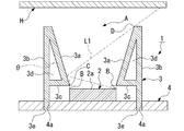
- the infrared sensor device 1 is installed with an opening A facing a measurement object H such as a fixing roller. Yes.
- This infrared sensor device 1 includes an infrared sensor main body 2, a cylindrical light guide member 3 that surrounds at least the light receiving surface 2a of the infrared sensor main body 2 and has an opening A immediately above the light receiving surface 2a, and an infrared sensor.
- a substrate 4 on which a main body 2 and a light guide member 3 are installed is provided.
- the infrared sensor body 2 is schematically shown.
- the light guide member 3 is formed of a plate material, and at least one of the surfaces surrounding the light receiving surface 2a is inclined plate portion 3a inclined with the light receiving surface 2a side facing the opening A side. Infrared reflecting surface composed of In the present embodiment, the inclined plate portions 3a are provided on two surfaces facing each other. The angle ⁇ formed by these inclined plate portions 3a is an angle in consideration of the case where the light that has reached the inside of the light guide member 3 is reflected once on the inner surface of the light guide member 3 before reaching the light receiving surface 2a.
- light (incident light L1) incident inside the light guide member 3 so as to contact the light guide tip D is reflected by the inner surface of the light guide member 3 opposite to the light guide tip D, the reflected light is guided.
- the light guide member 3 has a support plate portion 3 b that stands on the substrate 4 and supports the inclined plate portion 3 a in a state of being separated from the infrared sensor body 2 and the substrate 4.
- the support plate portion 3b is installed apart from the infrared sensor main body 2. Moreover, the lower part of the support plate part 3b is installed farther from the infrared sensor body 2 than the lower part of the inclined plate part 3a.
- the light guide member 3 has a lower support portion 3c connected to the lower end of the inclined plate portion 3a. That is, the upper end of the support plate portion 3b is connected to the upper end of the inclined plate portion 3a, and the lower end of the inclined plate portion 3a is connected to the lower support portion 3c.
- the lower support portion 3c is arranged in parallel with the substrate 4 and has a tip portion in contact with the support plate portion 3b. Therefore, the lower portion of the support plate portion 3b is installed on the substrate 4 at a distance from the infrared sensor body 2 than the lower end of the inclined plate portion 3a.
- the cavity 3d is formed between the support plate portion 3b and the inclined plate portion 3a by the lower support portion 3c. That is, a cavity 3d having a triangular cross section is formed between the support plate portion 3b and the inclined plate portion 3a.
- the support plate portion 3b, the inclined plate portion 3a, and the lower support portion 3c are formed of a thin metal plate such as stainless steel.
- the light guide member 3 has a rectangular tube shape as a whole, and has a plurality of fixing projections 3e inserted into a plurality of mounting holes 4a formed in the substrate 4 at the lower portion of the support plate portion 3b and the like. That is, the light guide member 3 is fixed on the substrate 4 by inserting the fixing protrusions 3 e into the mounting holes 4 a of the substrate 4. In addition, after inserting the fixing projection 3e into the mounting hole 4a, the tip of the fixing projection 3e may be bent and fixed so as not to come off.
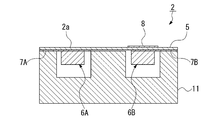
- the infrared sensor main body 2 includes an insulating film 5 having a light receiving surface 2a on the upper surface and a first thermal element 6A provided on the lower surface of the insulating film 5 so as to be separated from each other. And the second thermal element 6B and the conductive first wiring film 7A formed on the lower surface of the insulating film 5 and connected to the first thermal element 6A and the conductive element connected to the second thermal element 6B. Second wiring film 7B.
- the infrared sensor body 2 includes a resin-made terminal support 11 disposed on the lower surface side of the insulating film 5, and a plurality of lower portions provided on the terminal support 11 and disposed below the terminal support 11. And a mounting terminal 12.
- a light receiving surface 2a is provided in a region on the first heat sensitive element 6A side of the upper surface of the insulating film 5, and a region on the second heat sensitive element 6B side is a region shielded from infrared rays. .
- an infrared reflecting film 8 is patterned to shield infrared rays, and an infrared shielding region is provided.
- the infrared reflecting film 8 is provided on the upper surface of the insulating film 5 so as to face the second heat sensitive element 6B.
- the infrared reflection film 8 is formed in a rectangular shape in a region on the second heat sensitive element 6 ⁇ / b> B side on the upper surface of the insulating film 5.
- the infrared reflection film 8 is formed of a material having an infrared reflectance higher than that of the insulating film 5 and is formed by applying a gold plating film on a copper foil. In addition to the gold plating film, for example, a mirror-deposited aluminum vapor deposition film or an aluminum foil may be used.
- the infrared reflecting film 8 is formed to cover the second thermal element 6B with a size larger than that of the second thermal element 6B.
- the first heat sensitive element 6A and the second heat sensitive element 6B are chip thermistors in which terminal portions are formed at both ends.
- this thermistor there are thermistors such as NTC type, PTC type, CTR type, etc.
- NTC type thermistors are adopted as the first thermal element 6A and the second thermal element 6B.
- This thermistor is made of a thermistor material such as a Mn—Co—Cu-based material or a Mn—Co—Fe-based material.
- Adhesive electrodes 9A and 9B formed on the insulating film 5 are connected to one end of each of the first wiring film 7A and the second wiring film 7B, and the insulating film 5 is connected to the other end.
- the terminal electrodes 10A and 10B formed in the above are connected. Note that the terminal portions of the corresponding first heat sensitive element 6A and second heat sensitive element 6B are adhered to the adhesive electrodes 9A and 9B with a conductive adhesive such as solder.
- the terminal electrodes 10A and 10B are joined to a wiring (not shown) on the substrate 4 with a conductive adhesive such as solder.
- the board 4 is a circuit board such as a PCB board.
- the insulating film 5 is formed of a polyimide resin sheet in a rectangular shape, and the infrared reflecting film 8, the first wiring film 7A, and the second wiring film 7B are formed of copper foil. That is, these are formed by a double-sided flexible substrate in which the surface of the polyimide substrate that is the insulating film 5 is patterned with the copper foil that is the infrared reflecting film 8, the first wiring film 7A, and the second wiring film 7B. It was produced.
- the mounting terminal 12 is made of, for example, a tin-plated copper alloy.
- the mounting terminal 12 extends to the upper part of the terminal support 11 and is connected to the first terminal electrode 10A and the second terminal electrode 10B in the corresponding first wiring film 7A and second wiring film 7B. ing.
- the lower portion 12 a of the mounting terminal 12 is provided so as to protrude downward from the lower surface of the terminal support 11. That is, the mounting terminal 12 extends vertically, and the lower portion 12a protrudes downward from the lower surface of the terminal support 11, and the lower portion 12a further bends and protrudes laterally. It is formed in a letter shape.
- the mounting terminals 12 are respectively arranged in the vicinity of the four corners of the terminal support 11 and are incorporated into the terminal support 11 by insert molding or fitting.
- the terminal support 11 is made of a resin such as PPS (polyphenylene sulfide resin), and is formed in a frame shape along at least the outer edge of the insulating film 5. That is, the terminal support 11 is composed of an outer frame portion along the outer edge portion of the insulating film 5 and an intermediate frame portion that crosses an intermediate portion between the first thermal element 6A and the second thermal element 6B. ing.
- PPS polyphenylene sulfide resin
- the infrared sensor device 1 of the present embodiment when the detection temperature error was examined using, for example, a 10 cm square planar heating element as a planar heating element having a finite heating area, the detected temperature error was 1.2 ° C. However, as a comparison, when a simple rectangular cylindrical light guide member without the inclined plate portion 3a was used, the detected temperature error was 3.0 ° C. That is, compared with the case where the light guide member without the inclined plate portion 3a is used, the infrared sensor device 1 of the present embodiment greatly reduces the detected temperature error, and highly accurate temperature measurement is obtained.
- the light guide member 3 is formed of a plate material, and at least one of the surfaces surrounding the light receiving surface 2a has an opening on the light receiving surface 2a side. Since the infrared reflecting surface is composed of the inclined plate portion 3a inclined toward the portion A side, the inclined plate portion 3a itself of the plate material capable of reducing the volume can be inclined, so that the heat capacity can be reduced.
- the direct incident light that directly reaches the light receiving surface 2a after entering the light guide member 3 is restricted from entering the light receiving surface 2a and is reflected once by the light guide member 3 to receive light. Light components other than the primary reflected light reaching the surface 2a can be prevented from entering the light receiving surface 2a.
- the light guide member 3 has a support plate portion 3b that stands on the substrate 4 and supports the inclined plate portion 3a in a state of being separated from the infrared sensor main body 2 and the substrate 4, and the support plate portion 3b is an infrared sensor. Since the inclined plate portion 3 a and the support plate portion 3 b are not in contact with the infrared sensor main body 2, the thermal resistance increases because the inclined plate portion 3 a and the support plate portion 3 b are not in contact with the infrared sensor main body 2. Is prevented from being transmitted directly.
- the support plate part 3b since the lower part of the support plate part 3b is installed farther away from the infrared sensor main body 2 than the lower part of the inclined plate part 3a, the support plate part 3b is connected to the infrared sensor main body 2 regardless of the position of the inclined plate part 3a. It is possible to prevent heat from being transmitted from the support plate portion 3b to the infrared sensor main body 2 via the substrate 4 by being further away from.
- the heat capacity can be further lowered, so that the thermal response is fast, and further, the heat is transferred from the inclined plate portion 3a to the support plate portion 3b. Therefore, the heat transmitted from the support plate portion 3b to the substrate 4 and the infrared sensor main body 2 side can be further suppressed.
- the inclined state of the inclined plate portion 3a and the shape of the light guide member 3 can be stabilized.
- the temperature detection error resulting from the temperature change outside the light guide member 3 can be suppressed by forming the cavity 3d between the support plate portion 3b and the inclined plate portion 3a. Furthermore, since the lower support portion 3c is provided at the lower end of the inclined plate portion 3a, a relatively closed space (cavity 3d) is formed in the gap between the support plate portion 3b and the inclined plate portion 3a. Changes in the surface temperature of the plate portion 3a can be suppressed, and as a result, temperature detection errors of the infrared sensor device can be suppressed. In addition, since the first heat sensitive element 6A and the second heat sensitive element 6B are provided on the insulating film 5, heat transfer from the light guide member 3 to the heat sensitive element is further suppressed, and highly accurate measurement is possible. become.
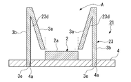
- the difference between the second embodiment and the first embodiment is that, in the first embodiment, the light guide member 3 has a lower support portion 3c, whereas the infrared sensor device 21 of the second embodiment is As shown in FIG. 5, the light guide member 23 has no lower support portion 3 c. Therefore, in the second embodiment, a gap 23d is formed instead of the cavity 3d between the support plate portion 3b and the inclined plate portion 3a.
- the gap 23d is formed between the support plate portion 3b and the inclined plate portion 3a, the heat capacity of the light guide member 23 can be reduced.
- the heat capacity of the light guide member 23 can be further reduced as compared with the first embodiment.
- the difference between the third embodiment and the second embodiment is that, in the second embodiment, a gap 23d is formed between the support plate portion 3b and the inclined plate portion 3a without the lower support portion 3c.
- a gap 33d is formed between the lower support portion 3c of the light guide member 33 and the inclined plate portion 3a. That is, in the third embodiment, the support plate portion 33b is low, the upper portion of the inclined plate portion 3a is not fixed to the support plate portion 33b, and the lower portion of the inclined plate portion 3a is fixed to the lower support portion 3c.
- the heat capacity of the light guide member 33 is reduced as in the second embodiment. Can be lowered. Moreover, the heat capacity of the light guide member 33 can be further reduced by the low support member 33b as compared with the first embodiment.
- the difference between the fourth embodiment and the second embodiment is that in the second embodiment, the lower portion of the support plate portion 23b is farther from the infrared sensor body 2 than the lower end of the inclined plate portion 3a.
- the infrared sensor device 41 of the fourth embodiment as shown in FIG. 7, the lower end of the inclined plate portion 3a is connected to the upper end of the support plate portion 43b, and the support plate portion 43b is close to the infrared sensor main body 2. It is a point. That is, in the fourth embodiment, the support plate portion 43b does not have the lower support portion 3c, and the inclined plate portion 3a is supported in an upright state on the upper portion of the support plate portion 43b.
- the support plate portion 43b is disposed at a position closer to the infrared sensor main body 2 than the lower end of the inclined plate portion 3a, the support plate portion 43b is connected to the infrared sensor main body 2 via the substrate 4 than in the second embodiment.
- the light guide member 43 itself can be made of less plate material, so that the heat capacity can be further reduced.
- the inclined plate portions are provided on the two surfaces facing each other.
- the inclined plate portion may be provided on at least one of the inner surfaces of the light guide member, and the heat source to be used (measurement object) ) And the like, the formation surface and angle of the inclined plate portion can be set.
- the light guide member is formed by bending one metal thin plate.
- the inclined plate portion 53a and the lower support portion 53c can be installed in a state where the locking portion 53f having a U-shaped cross section formed on the upper portion of the inclined plate portion 53a is hooked on the upper end of the support plate portion 53b.
- the first and second thermosensitive elements of the chip thermistor are employed.
- the first and second thermosensitive elements formed of the thin film thermistor are employed. It doesn't matter.
- a thin film thermistor or a chip thermistor is used as described above, but a pyroelectric element or the like can be used in addition to the thermistor.
Landscapes
- Physics & Mathematics (AREA)
- General Physics & Mathematics (AREA)
- Spectroscopy & Molecular Physics (AREA)
- Photometry And Measurement Of Optical Pulse Characteristics (AREA)
- Radiation Pyrometers (AREA)
Abstract
Description
例えば、特許文献1には、赤外線センサと光学レンズと導光器とを備えた非接触測温センサが記載されている。この非接触測温センサに用いられている導光器は、筐体に設けられた光学レンズに赤外線を導くように筐体に設置されており、厚みを変えてテーパ状とした内面を持っている。
すなわち、特許文献1の技術では、厚肉の導光器の厚さを変えてテーパ状の導光路が形成されているが、導光路の赤外線センサに近い部分が厚くなって体積が増加することで、導光器の熱容量が増加してしまい、導光路からの輻射や熱伝導が赤外線センサの感度や精度に大きく影響を与えてしまうという問題があった。
また、特許文献2の技術では、略直方体形状の筐体に導光路となる貫通孔が形成されているため、やはり導光路部材となる筐体自体の大きな体積に伴って熱容量が大きく、筐体からの輻射や熱伝導が赤外線センサの感度や精度に大きく影響を与えてしまう。
さらに、特許文献3の技術では、受光面に到達する赤外光を制御するための案内筒が薄い材料で形成されているものの、案内筒が内側に傾く勾配を有し、上部開口側の内径が小さくされた略台形形状を呈しているので、案内筒内の受光面へ所望の赤外光を導くために、導光器の寸法が大きくなってしまうという不都合があった。
すなわち、この赤外線センサ装置では、導光路部材が、基板上に立設され傾斜板部を赤外線センサ本体及び基板から離間した状態で支持する支持板部を有し、支持板部が、赤外線センサ本体から離間して設置されているので、傾斜板部及び支持板部が赤外線センサ本体に接触していないことで熱抵抗が大きくなり、導光路部材から赤外線センサ本体に熱が直接伝わることが抑制される。
すなわち、この赤外線センサ装置では、支持板部の下部が、傾斜板部の下部よりも赤外線センサ本体から離間して設置されているので、傾斜板部の位置にかかわらず支持板部を赤外線センサ本体からより離すことで、支持板部から基板を介して赤外線センサ本体に熱が伝わることを抑制することができる。
すなわち、この赤外線センサ装置では、支持板部と傾斜板部との間に隙間又は空洞が形成されているので、熱容量をさらに下げることができるため熱応答が速く、更に、傾斜板部から支持板部に熱が伝わり難く、支持板部から基板及び赤外線センサ本体側へ伝わる熱をさらに抑制することができる。また、支持板部と傾斜板部との間に隙間または空洞が形成されていることにより、導光路部材外部の温度変化に起因する温度検出誤差を抑制することができる。
すなわち、この赤外線センサ装置では、絶縁性フィルム上に感熱素子が設けられているので、導光路部材から感熱素子への熱伝達がさらに抑制されて高精度な測定が可能になる。
すなわち、本発明に係る赤外線センサ装置によれば、導光路部材が、板材で形成されていると共に、受光面を囲んでいる面のうち少なくとも1面が、受光面側の面を開口部側に向けて傾斜した傾斜板部で構成された赤外線反射面であるので、体積を小さくできる板材の傾斜板部自体が傾斜していることで、熱容量を小さくでき、また、導光路部材内部に入射された後、受光面に直接到達する直接入射光が、受光面に入射されることを規制すると共に、導光路部材において一回反射された後、受光面に到達する一次反射光以外の光成分が、受光面に入射されることを抑制することができる。
したがって、本発明の赤外線センサ装置は、熱容量の小さな導光路部材によって高い熱的応答性を得ることができると共に、視野角以外の光成分の抑制によって高い測定指向性を得ることができ、特に、複写機やプリンタ等のトナーの定着ローラを測定する温度センサとして好適である。
この赤外線センサ装置1は、赤外線センサ本体2と、赤外線センサ本体2の少なくとも受光面2aを囲んで設けられ受光面2aの直上に開口部Aを有した筒状の導光路部材3と、赤外線センサ本体2と導光路部材3とが設置された基板4とを備えている。なお、図1において、赤外線センサ本体2は、概略的に図示している。
θ以上に角度が大きくなると、受光面2aに到達する光線が減少するため、受光感度が犠牲になる。一方、θ以下の角度の場合、θの場合と比較して相対的に広い角度から光が入射されるため、温度誤差が大きくなる場合がある。また、上記のθが実現されていても、導光路部材3内部の傾斜板部3aが受光面2aを覆うと、受光面2aに到達する光量が減少するため、傾斜板部3aが受光面2aに被らないように設置することが好ましい。すなわち、傾斜板部基端部Cは、同じ側の受光面端部Bにおける受光面2a上部かつ受光平面に対する法線上に位置していることが望ましい。
上記支持板部3bは、赤外線センサ本体2から離間して設置されている。
また、支持板部3bの下部は、傾斜板部3aの下部よりも赤外線センサ本体2から離間して設置されている。
支持板部3b、傾斜板部3a及び下部支持部3cは、ステンレス等の金属薄板で形成されている。
また、赤外線センサ本体2は、絶縁性フィルム5の下面側に配された樹脂製の端子支持体11と、該端子支持体11に設けられ下部が端子支持体11の下部に配された複数の実装用端子12とを備えている。
上記第2の感熱素子6B側の領域には、赤外線反射膜8がパターン形成されて赤外線が遮蔽されており、赤外線を遮蔽した領域を設けている。
上記赤外線反射膜8は、絶縁性フィルム5よりも高い赤外線反射率を有する材料で形成され、銅箔上に金メッキ膜が施されて形成されている。なお、金メッキ膜の他に、例えば鏡面のアルミニウム蒸着膜やアルミニウム箔等で形成しても構わない。この赤外線反射膜8は、第2の感熱素子6Bよりも大きなサイズでこれを覆うように形成されている。
なお、上記接着電極9A,9Bには、それぞれ対応する第1の感熱素子6A及び第2の感熱素子6Bの端子部が半田等の導電性接着剤で接着される。
また、端子電極10A,10Bは、基板4上の配線(図示略)に半田等の導電性接着剤で接合されている。
上記基板4は、例えばPCB基板等の回路基板である。
また、実装用端子12の下部12aは、端子支持体11の下面よりも下方に突出して設けられている。すなわち、実装用端子12は、上下に延在し、下部12aが端子支持体11の下面よりも下方に突出していると共に、さらに下部12aが側方に向けて屈曲し突出しており、全体としてL字状に形成されている。
実装用端子12は、端子支持体11の四隅近傍にそれぞれ配置され、インサート成形や嵌め込み等によって端子支持体11内に組み込まれている。
特に、第1実施形態では、下部支持部3cによって傾斜板部3aの下端が支持されるため、傾斜板部3aの傾斜状態及び導光路部材3の形状を安定させることができる。
また、支持板部3bと傾斜板部3aとの間に空洞3dが形成されていることにより、導光路部材3外部の温度変化に起因する温度検出誤差を抑制することができる。更に、傾斜板部3aの下端に下部支持部3cを設けているので、支持板部3bと傾斜板部3aとの隙間に比較的閉ざされた空間(空洞3d)が形成されることにより、傾斜板部3a表面温度の変化を抑制でき、その結果、赤外線センサ装置の温度検出誤差を抑制することができる。
また、絶縁性フィルム5上に第1の感熱素子6A及び第2の感熱素子6Bが設けられているので、導光路部材3から感熱素子への熱伝達がさらに抑制されて高精度な測定が可能になる。
そのため、第2実施形態では、支持板部3bと傾斜板部3aとの間に空洞3dではなく隙間23dが形成されている。
すなわち、第3実施形態では、支持板部33bが低く、傾斜板部3aの上部が支持板部33bに固定されていないと共に、傾斜板部3aの下部が下部支持部3cに固定されている。
すなわち、第4実施形態では、支持板部43bが下部支持部3cを有さず、支持板部43bの上部に傾斜板部3aが立設状態で支持されている。
また、第1実施形態では、一枚の金属薄板を折り曲げて導光路部材を形成したが、図8に示す他の例のように、支持板部53bと、傾斜板部53a及び下部支持部53cとを別体の金属薄板で形成しても構わない。この場合、例えば支持板部53bの上端に、傾斜板部53aの上部に形成した断面コ字状の係止部53fを引っ掛けた状態で傾斜板部53a及び下部支持部53cを設置可能である。
なお、感熱素子としては、上述したように薄膜サーミスタやチップサーミスタが用いられるが、サーミスタ以外に焦電素子等も採用可能である。
Claims (5)
- 赤外線センサ本体と、
前記赤外線センサ本体の少なくとも受光面を囲んで設けられ前記受光面の直上に開口部を有した導光路部材とを備え、
前記導光路部材が、板材で形成されていると共に、前記受光面を囲んでいる面のうち少なくとも1面が、前記受光面側の面を前記開口部側に向けて傾斜した傾斜板部で構成された赤外線反射面とされていることを特徴とする赤外線センサ装置。 - 請求項1に記載の赤外線センサ装置において、
前記赤外線センサ本体と前記導光路部材とが設置された基板を備え、
前記導光路部材が、前記基板上に立設され前記傾斜板部を前記赤外線センサ本体及び前記基板から離間した状態で支持する支持板部を有し、
前記支持板部が、前記赤外線センサ本体から離間して設置されていることを特徴とする赤外線センサ装置。 - 請求項2に記載の赤外線センサ装置において、
前記支持板部の下部が、前記傾斜板部の下部よりも前記赤外線センサ本体から離間して設置されていることを特徴とする赤外線センサ装置。 - 請求項2に記載の赤外線センサ装置において、
前記支持板部と前記傾斜板部との間に隙間又は空洞が形成されていることを特徴とする赤外線センサ装置。 - 請求項1に記載の赤外線センサ装置において、
前記赤外線センサ本体が、前記受光面を上面に有する絶縁性フィルムと、
前記絶縁性フィルムの下面に互いに離間させて設けられた第1の感熱素子及び第2の感熱素子と、
前記絶縁性フィルムの下面に形成され前記第1の感熱素子に接続された導電性の第1の配線膜及び前記第2の感熱素子に接続された導電性の第2の配線膜とを備え、
前記絶縁性フィルムの上面のうち、前記第1の感熱素子側の領域に前記受光面が設けられていると共に、前記第2の感熱素子側の領域が赤外線を遮蔽した領域とされていることを特徴とする赤外線センサ装置。
Priority Applications (4)
| Application Number | Priority Date | Filing Date | Title |
|---|---|---|---|
| EP17756112.3A EP3421952A4 (en) | 2016-02-22 | 2017-01-31 | INFRARED SENSOR DEVICE |
| CN201780004571.4A CN108369136A (zh) | 2016-02-22 | 2017-01-31 | 红外线传感器装置 |
| KR1020187023362A KR20180114043A (ko) | 2016-02-22 | 2017-01-31 | 적외선 센서 장치 |
| US16/078,028 US20190049308A1 (en) | 2016-02-22 | 2017-01-31 | Infrared sensor apparatus |
Applications Claiming Priority (2)
| Application Number | Priority Date | Filing Date | Title |
|---|---|---|---|
| JP2016-030868 | 2016-02-22 | ||
| JP2016030868A JP6691681B2 (ja) | 2016-02-22 | 2016-02-22 | 赤外線センサ装置 |
Publications (1)
| Publication Number | Publication Date |
|---|---|
| WO2017145670A1 true WO2017145670A1 (ja) | 2017-08-31 |
Family
ID=59685375
Family Applications (1)
| Application Number | Title | Priority Date | Filing Date |
|---|---|---|---|
| PCT/JP2017/003440 Ceased WO2017145670A1 (ja) | 2016-02-22 | 2017-01-31 | 赤外線センサ装置 |
Country Status (6)
| Country | Link |
|---|---|
| US (1) | US20190049308A1 (ja) |
| EP (1) | EP3421952A4 (ja) |
| JP (1) | JP6691681B2 (ja) |
| KR (1) | KR20180114043A (ja) |
| CN (1) | CN108369136A (ja) |
| WO (1) | WO2017145670A1 (ja) |
Families Citing this family (6)
| Publication number | Priority date | Publication date | Assignee | Title |
|---|---|---|---|---|
| CN109416283B (zh) * | 2017-06-06 | 2019-12-24 | 株式会社芝浦电子 | 红外线温度传感器及其制造方法 |
| CN110260972A (zh) * | 2019-08-01 | 2019-09-20 | 河源鸿祺电子技术有限公司 | 照度检测装置 |
| CN111238659B (zh) * | 2020-01-20 | 2021-09-07 | 武汉高芯科技有限公司 | 一种具有抑制杂散光功能的冷屏及制冷型红外探测器 |
| KR102777324B1 (ko) * | 2021-10-20 | 2025-03-07 | 주식회사 케이티앤지 | 에어로졸 생성장치 |
| CN114705297A (zh) * | 2022-04-06 | 2022-07-05 | 浙江珏芯微电子有限公司 | 一种高效屏蔽的冷屏及红外探测器 |
| CN119290164A (zh) * | 2024-12-13 | 2025-01-10 | 翼捷安全设备(昆山)有限公司 | 一种红外热释电传感器、火灾探测器及气体分析仪 |
Citations (5)
| Publication number | Priority date | Publication date | Assignee | Title |
|---|---|---|---|---|
| JP2004257885A (ja) * | 2003-02-26 | 2004-09-16 | Horiba Ltd | 多素子型赤外線検出器 |
| JP2007501404A (ja) * | 2003-05-13 | 2007-01-25 | ハイマン・センサー・ゲゼルシャフト・ミット・ベシュレンクテル・ハフツング | 最適化された表面を活用する赤外線センサー |
| JP2011102791A (ja) * | 2009-10-17 | 2011-05-26 | Mitsubishi Materials Corp | 赤外線センサ及びこれを備えた回路基板 |
| JP2014225665A (ja) * | 2013-05-14 | 2014-12-04 | マイクロ・ハイブリッド エレクトロニック ゲーエムベーハー | 気密封止光電子変換又は電子光学変換部品及びその製造方法 |
| JP2016080556A (ja) * | 2014-10-20 | 2016-05-16 | 岡谷電機産業株式会社 | 赤外線センサ |
Family Cites Families (12)
| Publication number | Priority date | Publication date | Assignee | Title |
|---|---|---|---|---|
| US5018872A (en) * | 1988-11-01 | 1991-05-28 | Diatek, Inc. | Probe assembly for infrared thermometer |
| US20060153278A1 (en) * | 2005-01-11 | 2006-07-13 | Kun-Sung Chen | Ear thermometer |
| US20060198424A1 (en) * | 2005-03-02 | 2006-09-07 | Kun-Sung Chen | Probe structure for an ear thermometer |
| TWI274857B (en) * | 2006-03-03 | 2007-03-01 | Radiant Innovation | Structural improvement of a probe |
| US7988352B2 (en) * | 2006-11-01 | 2011-08-02 | Radiant Innovation Inc. | Probe structure |
| JP2008175720A (ja) * | 2007-01-19 | 2008-07-31 | Mitsubishi Electric Corp | 赤外線センサおよび赤外線センサアレイ |
| JP6131520B2 (ja) * | 2012-02-06 | 2017-05-24 | 三菱マテリアル株式会社 | 赤外線センサ装置 |
| US9273586B2 (en) * | 2012-08-03 | 2016-03-01 | Semitec Corporation | Contact-type infrared temperature sensor for high temperature measurement, thermal apparatus, and exhaust system |
| JP2014089108A (ja) * | 2012-10-30 | 2014-05-15 | Tdk Corp | 非接触温度センサ |
| KR20140042633A (ko) * | 2013-03-25 | 2014-04-07 | (주)아이엠 | 적외선센서모듈 |
| JP5488751B1 (ja) * | 2013-08-30 | 2014-05-14 | 富士ゼロックス株式会社 | 温度センサ、定着装置、および画像形成装置 |
| KR20150089251A (ko) * | 2014-01-27 | 2015-08-05 | 주식회사 퍼스트옵틱스 | 반사모듈 및 그를 가지는 초전 적외선센서모듈 |
-
2016
- 2016-02-22 JP JP2016030868A patent/JP6691681B2/ja not_active Expired - Fee Related
-
2017
- 2017-01-31 WO PCT/JP2017/003440 patent/WO2017145670A1/ja not_active Ceased
- 2017-01-31 US US16/078,028 patent/US20190049308A1/en not_active Abandoned
- 2017-01-31 EP EP17756112.3A patent/EP3421952A4/en not_active Withdrawn
- 2017-01-31 CN CN201780004571.4A patent/CN108369136A/zh active Pending
- 2017-01-31 KR KR1020187023362A patent/KR20180114043A/ko not_active Withdrawn
Patent Citations (5)
| Publication number | Priority date | Publication date | Assignee | Title |
|---|---|---|---|---|
| JP2004257885A (ja) * | 2003-02-26 | 2004-09-16 | Horiba Ltd | 多素子型赤外線検出器 |
| JP2007501404A (ja) * | 2003-05-13 | 2007-01-25 | ハイマン・センサー・ゲゼルシャフト・ミット・ベシュレンクテル・ハフツング | 最適化された表面を活用する赤外線センサー |
| JP2011102791A (ja) * | 2009-10-17 | 2011-05-26 | Mitsubishi Materials Corp | 赤外線センサ及びこれを備えた回路基板 |
| JP2014225665A (ja) * | 2013-05-14 | 2014-12-04 | マイクロ・ハイブリッド エレクトロニック ゲーエムベーハー | 気密封止光電子変換又は電子光学変換部品及びその製造方法 |
| JP2016080556A (ja) * | 2014-10-20 | 2016-05-16 | 岡谷電機産業株式会社 | 赤外線センサ |
Non-Patent Citations (1)
| Title |
|---|
| See also references of EP3421952A4 * |
Also Published As
| Publication number | Publication date |
|---|---|
| EP3421952A4 (en) | 2019-10-23 |
| CN108369136A (zh) | 2018-08-03 |
| US20190049308A1 (en) | 2019-02-14 |
| JP6691681B2 (ja) | 2020-05-13 |
| EP3421952A1 (en) | 2019-01-02 |
| JP2017150831A (ja) | 2017-08-31 |
| KR20180114043A (ko) | 2018-10-17 |
Similar Documents
| Publication | Publication Date | Title |
|---|---|---|
| WO2017145670A1 (ja) | 赤外線センサ装置 | |
| JP5832007B2 (ja) | 赤外線センサ及びその製造方法 | |
| CN102667430B (zh) | 非接触温度传感器 | |
| TWI526677B (zh) | Infrared sensor | |
| KR102610063B1 (ko) | 적외선 온도 센서, 회로 기판 및 상기 센서를 이용한 장치 | |
| TW201303271A (zh) | 紅外線感應器 | |
| WO2016152221A1 (ja) | 赤外線温度センサ及び赤外線温度センサを用いた装置 | |
| KR102610102B1 (ko) | 적외선 온도 센서 및 적외선 온도 센서를 이용한 장치 | |
| JP6016119B2 (ja) | 赤外線センサ装置 | |
| JP6477058B2 (ja) | 赤外線センサ | |
| JP6128374B2 (ja) | 赤外線センサ装置 | |
| JP2017181031A (ja) | 赤外線センサ | |
| JP2004354172A (ja) | 赤外線温度センサ | |
| JP2017181130A (ja) | 赤外線センサ装置 | |
| JP6620608B2 (ja) | 赤外線センサ | |
| JP5754223B2 (ja) | 定着装置 | |
| WO2020084809A1 (ja) | 赤外線センサ | |
| JP2020153667A (ja) | 導光路部材及びその製造方法 | |
| WO2020084811A1 (ja) | 赤外線センサ |
Legal Events
| Date | Code | Title | Description |
|---|---|---|---|
| ENP | Entry into the national phase |
Ref document number: 20187023362 Country of ref document: KR Kind code of ref document: A |
|
| NENP | Non-entry into the national phase |
Ref country code: DE |
|
| WWE | Wipo information: entry into national phase |
Ref document number: 2017756112 Country of ref document: EP |
|
| ENP | Entry into the national phase |
Ref document number: 2017756112 Country of ref document: EP Effective date: 20180924 |
|
| 121 | Ep: the epo has been informed by wipo that ep was designated in this application |
Ref document number: 17756112 Country of ref document: EP Kind code of ref document: A1 |