WO2017145809A1 - シリコン含有パターン反転用被覆剤 - Google Patents
シリコン含有パターン反転用被覆剤 Download PDFInfo
- Publication number
- WO2017145809A1 WO2017145809A1 PCT/JP2017/004921 JP2017004921W WO2017145809A1 WO 2017145809 A1 WO2017145809 A1 WO 2017145809A1 JP 2017004921 W JP2017004921 W JP 2017004921W WO 2017145809 A1 WO2017145809 A1 WO 2017145809A1
- Authority
- WO
- WIPO (PCT)
- Prior art keywords
- group
- acid
- methyl
- pattern
- polysiloxane
- Prior art date
- Legal status (The legal status is an assumption and is not a legal conclusion. Google has not performed a legal analysis and makes no representation as to the accuracy of the status listed.)
- Ceased
Links
Images


Classifications
-
- C—CHEMISTRY; METALLURGY
- C08—ORGANIC MACROMOLECULAR COMPOUNDS; THEIR PREPARATION OR CHEMICAL WORKING-UP; COMPOSITIONS BASED THEREON
- C08G—MACROMOLECULAR COMPOUNDS OBTAINED OTHERWISE THAN BY REACTIONS ONLY INVOLVING UNSATURATED CARBON-TO-CARBON BONDS
- C08G77/00—Macromolecular compounds obtained by reactions forming a linkage containing silicon with or without sulfur, nitrogen, oxygen or carbon in the main chain of the macromolecule
- C08G77/04—Polysiloxanes
- C08G77/06—Preparatory processes
-
- C—CHEMISTRY; METALLURGY
- C08—ORGANIC MACROMOLECULAR COMPOUNDS; THEIR PREPARATION OR CHEMICAL WORKING-UP; COMPOSITIONS BASED THEREON
- C08G—MACROMOLECULAR COMPOUNDS OBTAINED OTHERWISE THAN BY REACTIONS ONLY INVOLVING UNSATURATED CARBON-TO-CARBON BONDS
- C08G77/00—Macromolecular compounds obtained by reactions forming a linkage containing silicon with or without sulfur, nitrogen, oxygen or carbon in the main chain of the macromolecule
- C08G77/04—Polysiloxanes
- C08G77/14—Polysiloxanes containing silicon bound to oxygen-containing groups
- C08G77/16—Polysiloxanes containing silicon bound to oxygen-containing groups to hydroxyl groups
-
- C—CHEMISTRY; METALLURGY
- C09—DYES; PAINTS; POLISHES; NATURAL RESINS; ADHESIVES; COMPOSITIONS NOT OTHERWISE PROVIDED FOR; APPLICATIONS OF MATERIALS NOT OTHERWISE PROVIDED FOR
- C09D—COATING COMPOSITIONS, e.g. PAINTS, VARNISHES OR LACQUERS; FILLING PASTES; CHEMICAL PAINT OR INK REMOVERS; INKS; CORRECTING FLUIDS; WOODSTAINS; PASTES OR SOLIDS FOR COLOURING OR PRINTING; USE OF MATERIALS THEREFOR
- C09D183/00—Coating compositions based on macromolecular compounds obtained by reactions forming in the main chain of the macromolecule a linkage containing silicon, with or without sulfur, nitrogen, oxygen, or carbon only; Coating compositions based on derivatives of such polymers
- C09D183/04—Polysiloxanes
- C09D183/08—Polysiloxanes containing silicon bound to organic groups containing atoms other than carbon, hydrogen, and oxygen
-
- G—PHYSICS
- G03—PHOTOGRAPHY; CINEMATOGRAPHY; ANALOGOUS TECHNIQUES USING WAVES OTHER THAN OPTICAL WAVES; ELECTROGRAPHY; HOLOGRAPHY
- G03F—PHOTOMECHANICAL PRODUCTION OF TEXTURED OR PATTERNED SURFACES, e.g. FOR PRINTING, FOR PROCESSING OF SEMICONDUCTOR DEVICES; MATERIALS THEREFOR; ORIGINALS THEREFOR; APPARATUS SPECIALLY ADAPTED THEREFOR
- G03F7/00—Photomechanical, e.g. photolithographic, production of textured or patterned surfaces, e.g. printing surfaces; Materials therefor, e.g. comprising photoresists; Apparatus specially adapted therefor
- G03F7/0002—Lithographic processes using patterning methods other than those involving the exposure to radiation, e.g. by stamping
-
- G—PHYSICS
- G03—PHOTOGRAPHY; CINEMATOGRAPHY; ANALOGOUS TECHNIQUES USING WAVES OTHER THAN OPTICAL WAVES; ELECTROGRAPHY; HOLOGRAPHY
- G03F—PHOTOMECHANICAL PRODUCTION OF TEXTURED OR PATTERNED SURFACES, e.g. FOR PRINTING, FOR PROCESSING OF SEMICONDUCTOR DEVICES; MATERIALS THEREFOR; ORIGINALS THEREFOR; APPARATUS SPECIALLY ADAPTED THEREFOR
- G03F7/00—Photomechanical, e.g. photolithographic, production of textured or patterned surfaces, e.g. printing surfaces; Materials therefor, e.g. comprising photoresists; Apparatus specially adapted therefor
- G03F7/004—Photosensitive materials
- G03F7/075—Silicon-containing compounds
- G03F7/0752—Silicon-containing compounds in non photosensitive layers or as additives, e.g. for dry lithography
-
- G—PHYSICS
- G03—PHOTOGRAPHY; CINEMATOGRAPHY; ANALOGOUS TECHNIQUES USING WAVES OTHER THAN OPTICAL WAVES; ELECTROGRAPHY; HOLOGRAPHY
- G03F—PHOTOMECHANICAL PRODUCTION OF TEXTURED OR PATTERNED SURFACES, e.g. FOR PRINTING, FOR PROCESSING OF SEMICONDUCTOR DEVICES; MATERIALS THEREFOR; ORIGINALS THEREFOR; APPARATUS SPECIALLY ADAPTED THEREFOR
- G03F7/00—Photomechanical, e.g. photolithographic, production of textured or patterned surfaces, e.g. printing surfaces; Materials therefor, e.g. comprising photoresists; Apparatus specially adapted therefor
- G03F7/004—Photosensitive materials
- G03F7/075—Silicon-containing compounds
- G03F7/0757—Macromolecular compounds containing Si-O, Si-C or Si-N bonds
- G03F7/0758—Macromolecular compounds containing Si-O, Si-C or Si-N bonds with silicon- containing groups in the side chains
-
- G—PHYSICS
- G03—PHOTOGRAPHY; CINEMATOGRAPHY; ANALOGOUS TECHNIQUES USING WAVES OTHER THAN OPTICAL WAVES; ELECTROGRAPHY; HOLOGRAPHY
- G03F—PHOTOMECHANICAL PRODUCTION OF TEXTURED OR PATTERNED SURFACES, e.g. FOR PRINTING, FOR PROCESSING OF SEMICONDUCTOR DEVICES; MATERIALS THEREFOR; ORIGINALS THEREFOR; APPARATUS SPECIALLY ADAPTED THEREFOR
- G03F7/00—Photomechanical, e.g. photolithographic, production of textured or patterned surfaces, e.g. printing surfaces; Materials therefor, e.g. comprising photoresists; Apparatus specially adapted therefor
- G03F7/004—Photosensitive materials
- G03F7/09—Photosensitive materials characterised by structural details, e.g. supports, auxiliary layers
- G03F7/11—Photosensitive materials characterised by structural details, e.g. supports, auxiliary layers having cover layers or intermediate layers, e.g. subbing layers
-
- G—PHYSICS
- G03—PHOTOGRAPHY; CINEMATOGRAPHY; ANALOGOUS TECHNIQUES USING WAVES OTHER THAN OPTICAL WAVES; ELECTROGRAPHY; HOLOGRAPHY
- G03F—PHOTOMECHANICAL PRODUCTION OF TEXTURED OR PATTERNED SURFACES, e.g. FOR PRINTING, FOR PROCESSING OF SEMICONDUCTOR DEVICES; MATERIALS THEREFOR; ORIGINALS THEREFOR; APPARATUS SPECIALLY ADAPTED THEREFOR
- G03F7/00—Photomechanical, e.g. photolithographic, production of textured or patterned surfaces, e.g. printing surfaces; Materials therefor, e.g. comprising photoresists; Apparatus specially adapted therefor
- G03F7/26—Processing photosensitive materials; Apparatus therefor
- G03F7/30—Imagewise removal using liquid means
-
- G—PHYSICS
- G03—PHOTOGRAPHY; CINEMATOGRAPHY; ANALOGOUS TECHNIQUES USING WAVES OTHER THAN OPTICAL WAVES; ELECTROGRAPHY; HOLOGRAPHY
- G03F—PHOTOMECHANICAL PRODUCTION OF TEXTURED OR PATTERNED SURFACES, e.g. FOR PRINTING, FOR PROCESSING OF SEMICONDUCTOR DEVICES; MATERIALS THEREFOR; ORIGINALS THEREFOR; APPARATUS SPECIALLY ADAPTED THEREFOR
- G03F7/00—Photomechanical, e.g. photolithographic, production of textured or patterned surfaces, e.g. printing surfaces; Materials therefor, e.g. comprising photoresists; Apparatus specially adapted therefor
- G03F7/26—Processing photosensitive materials; Apparatus therefor
- G03F7/36—Imagewise removal not covered by groups G03F7/30 - G03F7/34, e.g. using gas streams, using plasma
-
- G—PHYSICS
- G03—PHOTOGRAPHY; CINEMATOGRAPHY; ANALOGOUS TECHNIQUES USING WAVES OTHER THAN OPTICAL WAVES; ELECTROGRAPHY; HOLOGRAPHY
- G03F—PHOTOMECHANICAL PRODUCTION OF TEXTURED OR PATTERNED SURFACES, e.g. FOR PRINTING, FOR PROCESSING OF SEMICONDUCTOR DEVICES; MATERIALS THEREFOR; ORIGINALS THEREFOR; APPARATUS SPECIALLY ADAPTED THEREFOR
- G03F7/00—Photomechanical, e.g. photolithographic, production of textured or patterned surfaces, e.g. printing surfaces; Materials therefor, e.g. comprising photoresists; Apparatus specially adapted therefor
- G03F7/26—Processing photosensitive materials; Apparatus therefor
- G03F7/40—Treatment after imagewise removal, e.g. baking
-
- H—ELECTRICITY
- H10—SEMICONDUCTOR DEVICES; ELECTRIC SOLID-STATE DEVICES NOT OTHERWISE PROVIDED FOR
- H10P—GENERIC PROCESSES OR APPARATUS FOR THE MANUFACTURE OR TREATMENT OF DEVICES COVERED BY CLASS H10
- H10P76/00—Manufacture or treatment of masks on semiconductor bodies, e.g. by lithography or photolithography
-
- C—CHEMISTRY; METALLURGY
- C08—ORGANIC MACROMOLECULAR COMPOUNDS; THEIR PREPARATION OR CHEMICAL WORKING-UP; COMPOSITIONS BASED THEREON
- C08G—MACROMOLECULAR COMPOUNDS OBTAINED OTHERWISE THAN BY REACTIONS ONLY INVOLVING UNSATURATED CARBON-TO-CARBON BONDS
- C08G77/00—Macromolecular compounds obtained by reactions forming a linkage containing silicon with or without sulfur, nitrogen, oxygen or carbon in the main chain of the macromolecule
- C08G77/04—Polysiloxanes
- C08G77/22—Polysiloxanes containing silicon bound to organic groups containing atoms other than carbon, hydrogen and oxygen
- C08G77/24—Polysiloxanes containing silicon bound to organic groups containing atoms other than carbon, hydrogen and oxygen halogen-containing groups
Definitions
- the present invention relates to a stepped substrate flattening composition applied on an organic pattern, comprising a specific polysiloxane containing a hydrolysis condensate of a hydrolyzable silane raw material and a solvent, a method for producing the same, and the composition.
- the present invention relates to a method for manufacturing a used semiconductor device.
- a technique for forming a fine pattern on a substrate and etching the substrate in accordance with this pattern to process the substrate is widely used in the field of semiconductor manufacturing.
- a pattern inversion method as one of the pattern forming techniques.
- a resist pattern is formed on the semiconductor substrate, and the resist pattern is covered with a silicon coating solution.
- the silicon-based coating liquid is filled between the resist patterns, and then baked to form a coating film.
- the upper part of the silicon-containing coating is etched back with a fluorine-based gas to expose the upper part of the resist pattern, and the gas is changed to remove the resist pattern with an oxygen-based etching gas.
- a silicon-based pattern derived from the film remains and the pattern is inverted.
- the reverse pattern is transferred to form a pattern on the substrate.
- a material using a polysiloxane and an ether solvent obtained by cohydrolysis of a silane having a group or an aryl group and tetraethoxysilane see Patent Document 1.
- the present invention uses a specific silicon-containing composition that can be satisfactorily embedded between resist patterns with respect to a stepped substrate having a difference in height or density in a resist pattern formed on a substrate to be processed, and steps according to a specific procedure.
- a method for flatly coating a substrate is provided.
- the present invention includes the following.
- a composition for planarizing an organic pattern applied on an organic pattern comprising a polysiloxane containing a hydrolysis condensate of a hydrolyzable silane raw material and a solvent,
- the polysiloxane contains silanol groups at a ratio of 20 mol% or less with respect to Si atoms,
- the composition wherein the polysiloxane has a weight average molecular weight of 1,000 to 50,000.
- the polysiloxane has the formula (1): (In Formula (1), R 1 represents an alkyl group, an aryl group, a halogenated alkyl group, a halogenated aryl group, an alkoxyaryl group, an alkenyl group, or an epoxy group, an acryloyl group, a methacryloyl group, a mercapto group, or a cyano group.
- a hydrolyzable silane represented by R 2 is an alkoxy group, an acyloxy group, or a halogen group, and a is 1.
- composition according to [1] comprising a hydrolysis condensate of a hydrolyzable silane raw material containing [3]
- the polysiloxane is 100 to 50 mol%, preferably 95 to 50 mol% of a hydrolyzable silane represented by the above formula (1) and a is 1, and represented by the above formula (1).
- composition according to [2] comprising a hydrolyzable condensate of a hydrolyzable silane raw material containing 0 to 50 mol%, preferably 5 to 50 mol% of a hydrolyzable silane in which a is 2 .
- the polysiloxane is 0 to 100 mol%, preferably 1 to 100 mol% of hydrolyzable silane in which a is 0 in the formula (1), and 0 to 0 hydrolyzable silane in which a is 1.
- the polysiloxane is a treatment product of a non-alcohol and a weak acid or base of a hydrolyzable condensate of the hydrolyzable silane raw material in which a in formula (1) is 1 or 2, [2] or [ 3].
- the weak acid is an acid having an acid dissociation constant of 4 to 5.
- the organic pattern is selected from a resist pattern, a nanoimprint pattern, and an organic underlayer film pattern.
- a step (1a) of forming a resist on the substrate, a step (2) of exposing and developing the resist, and a resist pattern during or after development A method for manufacturing a semiconductor device, comprising: a step (3a) of applying a composition; and a step (4a) of removing a resist pattern by etching to reverse the pattern.
- the production method according to [9] including a step (1a-1) of forming a resist underlayer film on the substrate before the step (1a).
- R 1 represents an alkyl group, an aryl group, a halogenated alkyl group, a halogenated aryl group, an alkoxyaryl group, an alkenyl group, or an epoxy group, an acryloyl group, a methacryloyl group, a mercapto group, or a cyano group.
- R 2 represents an alkoxy group, an acyloxy group, or a halogen group, a represents 0), and a represents 0 0 to 100 mol%, preferably 1 to 100 mol%, and 0 to 100 mol%, preferably 0 to 99 mol, of the hydrolyzable silane represented by the formula (1) and a is 1.
- the manufacturing method including the process of dehydrating the hydrolysis-condensation product of the hydrolysable silane raw material contained in the ratio used as mol% with alcohol and an acid.
- a method for producing a polysiloxane contained in a stepped substrate planarizing composition applied to an organic pattern Formula (1):
- R 1 represents an alkyl group, an aryl group, a halogenated alkyl group, a halogenated aryl group, an alkoxyaryl group, an alkenyl group, or an epoxy group, an acryloyl group, a methacryloyl group, a mercapto group, or a cyano group.
- An organic group having a silicon atom bonded to the silicon atom by a Si—C bond R 2 represents an alkoxy group, an acyloxy group, or a halogen group, and a represents 1 or 2.
- the manufacturing method including the process of processing the hydrolysis condensate of 1 or 2 hydrolysable silane raw materials with a non-alcohol and a weak acid or a base.
- the composition for planarizing a stepped substrate of the present invention is coated on the patterned organic underlayer film without mixing with the patterned organic underlayer film formed on the substrate to be processed. It is possible to satisfactorily fill (fill) between film patterns.
- the stepped substrate planarizing composition is cured to form a polysiloxane composition film, and a flat surface can be formed later by etching back by etching (gas etching).
- the organic underlayer film can be removed by ashing (ashing treatment)
- the pattern of the organic underlayer film is reversed to the pattern of the polysiloxane composition film formed by filling the stepped substrate planarizing composition. it can.
- the substrate to be processed can be processed by these reversal patterns.
- a method of filling (filling) a polysiloxane composition between photoresist patterns and then inverting the polysiloxane pattern by etching with an oxygen-based gas has been performed.
- the resist film is thin, a high aspect ratio inversion pattern cannot be obtained.
- the pattern can be reversed using a stepped substrate having a larger aspect ratio than the photoresist pattern on the substrate to be processed, and as a result, a reversed pattern having a high aspect ratio can be obtained.
- an organic underlayer film having a large aspect ratio can be embedded between patterns, coating with a specific polysiloxane composition is effective.
- a method of embedding (filling) a polysiloxane composition between photoresist patterns is difficult to perform ashing or the like because an organic film exists in the lower layer, and may be performed by gas etching. Many.
- the organic underlayer film on the substrate to be processed or on the oxide film can be reversed with the polysiloxane composition, it is cured after embedding the polysiloxane composition. The pattern can be easily reversed by the ashing process.
- the step can be completely flattened, and the super flatness of the coating film can be realized.
- flattening is a coated coating in which a portion where a resist pattern exists (line portion) and a portion where a pattern does not exist (space portion) are present on the top when applied to a resist pattern. This means that there is little difference in film thickness.
- Step Substrate Flattening Composition The step substrate flattening composition according to the present invention will be described below.
- the step substrate flattening composition (sometimes referred to as a coating polysiloxane composition) according to the present invention is applied to the resist pattern during or after development.
- a silicon hard mask may partially remain on the upper surface of the organic underlayer film. This is because the stepped substrate planarizing composition later exposes the upper surface of the organic underlayer film by etch back, so that the coating polysiloxane and the silicon hard mask are simultaneously removed by etch back.
- the polysiloxane contains silanol groups at a ratio of 20 mol% or less with respect to Si atoms.
- the proportion of silanol groups can be 5-20 mol%, or 10-20 mol%.
- the silanol group ratio in the polysiloxane can be calculated by 1 H NMR.
- the polysiloxane has a weight average molecular weight of 1,000 to 50,000.
- a preferred weight average molecular weight is 1,200 to 20,000.
- Polysiloxane usually contains a hydrolysis condensate of a hydrolyzable silane raw material.
- the hydrolyzable silane raw material can contain one or more silanes.
- the polysiloxane has the formula (1): (In Formula (1), R 1 represents an alkyl group, an aryl group, a halogenated alkyl group, a halogenated aryl group, an alkoxyaryl group, an alkenyl group, or an epoxy group, an acryloyl group, a methacryloyl group, a mercapto group, or a cyano group.
- a hydrolyzable silane represented by R 2 is an alkoxy group, an acyloxy group, or a halogen group, and a is 1. The hydrolysis condensate of the hydrolysable silane raw material containing this is included.
- the polysiloxane is 100 to 50 mol%, more preferably 95 to 50 mol%, and more preferably 95 to 50 mol% of a hydrolyzable silane represented by the above formula (1) and a is 1.
- the hydrolyzable silane in which a is 1 in the formula (1) is 95 to 70 mol% and the hydrolyzable silane in which a is 2 in the formula (1) is 5 to 30 mol%.
- the polysiloxane is a hydrolyzable silane in which a in formula (1) is 0 to 0 to 100 mol%, more preferably 1 to 100 mol%, and a is 1
- a dehydration product of polysiloxane containing a hydrolyzable condensate of a hydrolyzable silane starting material in a proportion of 0 to 100 mol%, more preferably 0 to 99 mol%, with an alcohol and an acid.
- the polysiloxane is a treatment product of a non-alcohol of a polysiloxane containing a hydrolysis condensate of a hydrolyzable silane raw material having a of 1 or 2 in the formula (1) and a weak acid or base. More preferably, the weak acid is an acid having an acid dissociation constant of 4-5.
- hydrolysis condensate can also use a hydrolyzable silane raw material or its hydrolyzate as a mixture.
- a hydrolysis-condensation product a partial hydrolysis product or a silane compound in which hydrolysis is not completely completed are mixed with the hydrolysis-condensation product, and the mixture can also be used.
- This condensate is a polymer having a polysiloxane structure.
- an organic acid having an acid dissociation constant (pka) of ⁇ 1 to 5, preferably 4 to 5 can be used.
- the acid can be exemplified by trifluoroacetic acid, maleic acid, benzoic acid, isobutyric acid, acetic acid, etc., among which benzoic acid, isobutyric acid, acetic acid, and the like.
- the acid is preferably an acid having a boiling point of 70 to 160 ° C. Examples thereof include trifluoroacetic acid, isobutyric acid, acetic acid and the like.
- the acid preferably has an acid dissociation constant (pka) of 4 to 5 or a boiling point of 70 to 160 ° C. and has any physical property. That is, those having low acidity or those having high acidity but low boiling point can be used.
- any property can be utilized from the properties of acid dissociation constant and boiling point, but acetic acid having both properties can be preferably used.
- the raw material used in the present invention, and the polysiloxane may be a hydrolytic condensate obtained by hydrolyzing and condensing at least one hydrolyzable silane raw material selected from the group consisting of formula (1).
- the organic pattern is a resist pattern. More preferably, the organic pattern is a nanoimprint pattern. More preferably, the organic pattern is an organic underlayer film pattern (patterned by processing an organic underlayer film (coating type or vapor deposition type)). Among these, a resist pattern is particularly preferable.
- the stepped substrate planarizing composition of the present invention includes a hydrolyzable condensate of hydrolyzable silane as represented by the above formula (1) and a solvent.
- a hydrolyzable condensate of hydrolyzable silane as represented by the above formula (1)
- a solvent as optional components, acid, water, alcohol, curing catalyst, acid generator, other organic polymer, light-absorbing compound, surfactant and the like can be included.
- the solid content in the stepped substrate planarizing composition of the present invention is, for example, 0.1 to 50% by mass, 0.1 to 30% by mass, 0.1 to 25% by mass, 0.5 to 20.0% by mass, Alternatively, the content is 1.0 to 10.0% by mass.
- the solid content is obtained by removing the solvent component from all the components of the stepped substrate planarizing composition.
- the proportion of the hydrolyzable silane, its hydrolyzate, and its hydrolysis condensate in the solid content is 20% by mass or more, for example, 50 to 100% by mass, 60 to 99% by mass, 70 to 99% by mass. It is.
- the concentration of the hydrolyzable silane, its hydrolyzate, and its hydrolysis condensate (polysiloxane) in the composition is 0.5 to 20.0% by mass.
- the coating composition since the coating composition is used after exposure of the resist, the resist is exposed through a mask and filled with the composition during or after development.
- the hydrolyzable silane, its hydrolyzate, and its hydrolysis condensate have a resin component different from that of the resist.
- a new pattern is formed by the hydrolyzed condensate (polysiloxane) filled by selectively removing the resist by dry etching by selecting the gas type.
- hydrolyzable silane, its hydrolyzate, and its hydrolysis condensate can also be used as a mixture thereof. It can be used as a condensate obtained by hydrolyzing a hydrolyzable silane and condensing the obtained hydrolyzate.
- a hydrolysis-condensation product a partial hydrolysis product or a silane compound in which hydrolysis is not completely completed are mixed with the hydrolysis-condensation product, and the mixture can also be used.
- This condensate is a polymer having a polysiloxane structure.
- alkyl group examples include straight-chain or branched alkyl groups having 1 to 10 carbon atoms, such as methyl group, ethyl group, n-propyl group, i-propyl group, n-butyl group, i- Butyl, s-butyl, t-butyl, n-pentyl, 1-methyl-n-butyl, 2-methyl-n-butyl, 3-methyl-n-butyl, 1,1-dimethyl -N-propyl group, 1,2-dimethyl-n-propyl group, 2,2-dimethyl-n-propyl group, 1-ethyl-n-propyl group, n-hexyl, 1-methyl-n-pentyl group, 2-methyl-n-pentyl group, 3-methyl-n-pentyl group, 4-methyl-n-pentyl group, 1,1-dimethyl-n-butyl group, 1,2-dimethyl-n-butyl group, 1,2-
- Cyclic alkyl groups can also be used.
- examples of the cyclic alkyl group having 1 to 10 carbon atoms include cyclopropyl group, cyclobutyl group, 1-methyl-cyclopropyl group, 2-methyl-cyclopropyl group, cyclopentyl group, 1 -Methyl-cyclobutyl group, 2-methyl-cyclobutyl group, 3-methyl-cyclobutyl group, 1,2-dimethyl-cyclopropyl group, 2,3-dimethyl-cyclopropyl group, 1-ethyl-cyclopropyl group, 2- Ethyl-cyclopropyl group, cyclohexyl group, 1-methyl-cyclopentyl group, 2-methyl-cyclopentyl group, 3-methyl-cyclopentyl group, 1-ethyl-cyclobutyl group, 2-ethyl-cyclobutyl group, 3-ethyl-cyclobutyl group 1,2-dimethyl-cyclobutyl group
- alkenyl group examples include alkenyl groups having 2 to 10 carbon atoms such as ethenyl group, 1-propenyl group, 2-propenyl group, 1-methyl-1-ethenyl group, 1-butenyl group and 2-butenyl group.
- aryl group examples include aryl groups having 6 to 20 carbon atoms, such as a phenyl group, o-methylphenyl group, m-methylphenyl group, p-methylphenyl group, o-chlorophenyl group, m- Chlorphenyl group, p-chlorophenyl group, o-fluorophenyl group, p-mercaptophenyl group, o-methoxyphenyl group, p-methoxyphenyl group, p-aminophenyl group, p-cyanophenyl group, ⁇ -naphthyl group ⁇ -naphthyl group, o-biphenylyl group, m-biphenylyl group, p-biphenylyl group, 1-anthryl group, 2-anthryl group, 9-anthryl group, 1-phenanthryl group, 2-phenanthryl group, 3-phenanthryl group , 4-
- Typical organic groups having the above epoxy group include glycidoxymethyl, glycidoxyethyl, glycidoxypropyl, glycidoxybutyl, epoxycyclohexyl and the like.
- Typical organic groups having the acryloyl group include acryloylmethyl, acryloylethyl, acryloylpropyl and the like.
- Typical organic groups having the methacryloyl group include methacryloylmethyl, methacryloylethyl, methacryloylpropyl and the like.
- Typical examples of the organic group having the mercapto group include ethyl mercapto, butyl mercapto, hexyl mercapto, octyl mercapto and the like.
- Typical organic groups having the cyano group include cyanoethyl, cyanopropyl and the like.
- alkoxy group examples include an alkoxy group having a linear, branched or cyclic alkyl portion having 1 to 20 carbon atoms, such as a methoxy group, an ethoxy group, an n-propoxy group, an i-propoxy group, n -Butoxy group, i-butoxy group, s-butoxy group, t-butoxy group, n-pentyloxy group, 1-methyl-n-butoxy group, 2-methyl-n-butoxy group, 3-methyl-n-butoxy group 1,1-dimethyl-n-propoxy group, 1,2-dimethyl-n-propoxy group, 2,2-dimethyl-n-propoxy group, 1-ethyl-n-propoxy group, n-hexyloxy group, 1- Methyl-n-pentyloxy group, 2-methyl-n-pentyloxy group, 3-methyl-n-pentyloxy group, 4-methyl-n-pentyloxy group, 1,1-dimethyl-n
- acyloxy group examples include the acyloxy groups having 2 to 20 carbon atoms, such as methylcarbonyloxy group, ethylcarbonyloxy group, n-propylcarbonyloxy group, i-propylcarbonyloxy group, n-butyl.
- halogen group examples include fluorine, chlorine, bromine and iodine.
- groups described above also apply to the alkyl group, aryl group, alkoxy group, and halogen group portion in the halogenated alkyl group, halogenated aryl group, and alkoxyaryl group.
- R 1 is preferably a methyl group, or a phenyl group which may be substituted with a halogen group or an alkoxy group.
- a stepped substrate flattening composition containing the hydrolysis condensate of the hydrolyzable silane raw material as described above and a crosslinkable compound having 2 to 6 methoxymethyl groups per molecule is used.
- a crosslinkable compound having 2 to 6 methoxymethyl groups per molecule include melamine type, substituted urea type, and polymer type thereof.
- a cross-linking agent having a cross-linking substituent, methoxymethylated glycoluril, butoxymethylated glycoluril, methoxymethylated melamine, butoxymethylated melamine, methoxymethylated benzoguanamine, butoxymethylated benzoguanamine, methoxymethylated urea , Butoxymethylated urea, methoxymethylated thiourea, or methoxymethylated thiourea.
- the condensate of these compounds can also be used.
- the addition amount of the crosslinking agent varies depending on the coating solvent used, the base substrate used, the required solution viscosity, the required film shape, etc., but is 0.001 to 80% by mass, preferably based on the total solid content. 0.01 to 50% by mass, more preferably 0.05 to 40% by mass.
- p-toluenesulfonic acid as a catalyst for promoting the crosslinking reaction, p-toluenesulfonic acid, trifluoromethanesulfonic acid, pyridinium p-toluenesulfonic acid, salicylic acid, sulfosalicylic acid, citric acid, benzoic acid, hydroxybenzoic acid, naphthalenecarboxylic acid Acidic compounds such as acids or / and thermal acid generators such as 2,4,4,6-tetrabromocyclohexadienone, benzoin tosylate, 2-nitrobenzyl tosylate, and other organic sulfonic acid alkyl esters may be added. I can do it.
- the blending amount is 0.0001 to 20% by mass, preferably 0.0005 to 10% by mass, preferably 0.01 to 3% by mass, based on the total solid content.
- hydrolysis condensate polysiloxane
- the hydrolysis condensate (polyorganosiloxane) of the above hydrolyzable silane raw material can provide a condensate having a weight average molecular weight of 1,000 to 50,000. These molecular weights are molecular weights obtained in terms of polystyrene by GPC analysis.
- GPC measurement conditions are, for example, GPC apparatus (trade name HLC-8220 GPC, manufactured by Tosoh Corporation), GPC column (trade names Shodex KF803L, KF802, KF801, Showa Denko), column temperature is 40 ° C., eluent (elution solvent) Is tetrahydrofuran, the flow rate (flow rate) is 1.0 ml / min, and the standard sample is polystyrene (made by Showa Denko KK).
- hydrolysis of the alkoxysilyl group, acyloxysilyl group, or halogenated silyl group 0.5 to 100 mol, preferably 1 to 10 mol of water is used per mol of the hydrolyzable group.
- a hydrolysis catalyst can be used for hydrolysis, it can also be performed without using a hydrolysis catalyst.
- 0.001 to 10 mol, preferably 0.001 to 1 mol of the hydrolysis catalyst can be used per mol of the hydrolyzable group.
- the reaction temperature during the hydrolysis and condensation is usually 20 to 110 ° C. Hydrolysis may be performed completely or partially. That is, a hydrolyzate or a monomer may remain in the hydrolysis condensate.
- a catalyst can be used for hydrolysis and condensation.
- An acid or a base can be used as the hydrolysis catalyst.
- the hydrolysis catalyst include metal chelate compounds, organic acids, inorganic acids, organic bases, and inorganic bases.
- Examples of the metal chelate compound as the hydrolysis catalyst include triethoxy mono (acetylacetonato) titanium, tri-n-propoxy mono (acetylacetonato) titanium, tri-i-propoxy mono (acetylacetonato) titanium, tri -N-Butoxy mono (acetylacetonato) titanium, tri-sec-butoxy mono (acetylacetonato) titanium, tri-t-butoxy mono (acetylacetonato) titanium, diethoxy bis (acetylacetonato) titanium , Di-n-propoxy bis (acetylacetonato) titanium, di-i-propoxy bis (acetylacetonato) titanium, di-n-butoxy bis (acetylacetonato) titanium, di-sec-butoxy bis (Acetylacetonate) titanium, di-t Butoxy bis (acetylacetonato) titanium, monoethoxy tris (acetylacetonato) titanium
- Organic acids as hydrolysis catalysts are, for example, acetic acid, propionic acid, butanoic acid, pentanoic acid, hexanoic acid, heptanoic acid, octanoic acid, nonanoic acid, decanoic acid, oxalic acid, maleic acid, methylmalonic acid, adipic acid, sebacin Acid, gallic acid, butyric acid, merit acid, arachidonic acid, 2-ethylhexanoic acid, oleic acid, stearic acid, linoleic acid, linolenic acid, salicylic acid, benzoic acid, p-aminobenzoic acid, p-toluenesulfonic acid, benzenesulfone Examples include acid, monochloroacetic acid, dichloroacetic acid, trichloroacetic acid, trifluoroacetic acid, formic acid, malonic acid, sulfonic acid, phthal
- Examples of the inorganic acid as the hydrolysis catalyst include hydrochloric acid, nitric acid, sulfuric acid, hydrofluoric acid, phosphoric acid and the like.
- Organic bases as hydrolysis catalysts include, for example, pyridine, pyrrole, piperazine, pyrrolidine, piperidine, picoline, trimethylamine, triethylamine, monoethanolamine, diethanolamine, dimethylmonoethanolamine, monomethyldiethanolamine, triethanolamine, diazabicyclooctane, diazine.
- Examples include zabicyclononane, diazabicycloundecene, and tetramethylammonium hydroxide.
- the inorganic base include ammonia, sodium hydroxide, potassium hydroxide, barium hydroxide, calcium hydroxide and the like. Of these catalysts, metal chelate compounds, organic acids, and inorganic acids are preferred, and these may be used alone or in combination of two or more.
- organic solvent used in the hydrolysis examples include n-pentane, i-pentane, n-hexane, i-hexane, n-heptane, i-heptane, 2,2,4-trimethylpentane, n-octane, i- Aliphatic hydrocarbon solvents such as octane, cyclohexane and methylcyclohexane; benzene, toluene, xylene, ethylbenzene, trimethylbenzene, methylethylbenzene, n-propylbenzene, i-propylbenzene, diethylbenzene, i-butylbenzene, triethylbenzene, di -Aromatic hydrocarbon solvents such as i-propyl benzene, n-amyl naphthalene, trimethylbenzene; methanol, ethanol, n-
- acetone methyl ethyl ketone, methyl-n-propyl ketone, methyl-n-butyl ketone, diethyl ketone, methyl-i-butyl ketone, methyl-n-pentyl ketone, ethyl-n-butyl ketone, methyl-n-hexyl ketone, di- Ketone solvents such as i-butyl ketone, trimethylnonanone, cyclohexanone, methylcyclohexanone, 2,4-pentanedione, acetonylacetone, diacetone alcohol, acetophenone, and fenchon are preferred from the viewpoint of storage stability of the solution.
- the step substrate flattening composition of the present invention can contain a curing catalyst.
- the curing catalyst functions as a curing catalyst when a coating film containing polyorganosiloxane composed of a hydrolysis condensate is heated and cured.
- As the curing catalyst ammonium salts, phosphines, phosphonium salts, and sulfonium salts can be used.
- the formula (D-1) (Wherein m represents an integer of 2 to 11, n represents an integer of 2 to 3, R 21 represents an alkyl group or an aryl group, and Y ⁇ represents an anion.)
- the formula (D-7) (Wherein, R 31, R 32, R 33, and R 34 represents an alkyl group or an aryl group, P is a phosphorus atom, Y - represents an anion, and R 31, R 32, R 33 , and R 34 Are each bonded to a phosphorus atom by a CP bond).
- the formula (D-8) (However, R 35 , R 36 , and R 37 are alkyl groups or aryl groups, S is a sulfur atom, Y ⁇ is an anion, and R 35 , R 36 , and R 37 are CS bonds, respectively. And a tertiary sulfonium salt which is bonded to a sulfur atom.
- the compound of the above formula (D-1) is a quaternary ammonium salt derived from an amine, m represents an integer of 2 to 11, and n represents an integer of 2 to 3.
- R 21 of this quaternary ammonium salt represents an alkyl group or aryl group having 1 to 18 carbon atoms, preferably 2 to 10 carbon atoms, such as a linear alkyl group such as an ethyl group, a propyl group or a butyl group, a benzyl group, Cyclohexyl group, cyclohexylmethyl group, dicyclopentadienyl group and the like.
- Anions (Y ⁇ ) include halogen ions such as chlorine ions (Cl ⁇ ), bromine ions (Br ⁇ ), iodine ions (I ⁇ ), carboxylates (—COO—), sulfonates (—SO 3 —). And acid groups such as alcoholate (—O—).
- the compound of the above formula (D-2) is a quaternary ammonium salt represented by R 22 R 23 R 24 R 25 N + Y ⁇ .
- R 22 , R 23 , R 24 and R 25 are an alkyl group or aryl group having 1 to 18 carbon atoms, or a silane compound bonded to a silicon atom by a Si—C bond.
- Anions (Y ⁇ ) include halogen ions such as chlorine ions (Cl ⁇ ), bromine ions (Br ⁇ ), iodine ions (I ⁇ ), carboxylates (—COO—), sulfonates (—SO 3 —), An acid group such as alcoholate (—O—) can be mentioned.
- This quaternary ammonium salt can be obtained commercially, for example, tetramethylammonium acetate, tetrabutylammonium acetate, triethylbenzylammonium chloride, triethylbenzylammonium bromide, trioctylmethylammonium chloride, tributylbenzyl chloride. Examples include ammonium and trimethylbenzylammonium chloride.
- the compound of the above formula (D-3) is a quaternary ammonium salt derived from 1-substituted imidazole
- R 26 and R 27 are an alkyl group or aryl group having 1 to 18 carbon atoms
- R 26 And the total number of carbon atoms of R 27 is preferably 7 or more.
- R 26 can be exemplified by methyl group, ethyl group, propyl group, phenyl group and benzyl group
- R 27 can be exemplified by benzyl group, octyl group and octadecyl group.
- Anions (Y ⁇ ) include halogen ions such as chlorine ions (Cl ⁇ ), bromine ions (Br ⁇ ), iodine ions (I ⁇ ), carboxylates (—COO—), sulfonates (—SO 3 —), An acid group such as alcoholate (—O—) can be mentioned.
- This compound can be obtained as a commercial product.
- imidazole compounds such as 1-methylimidazole and 1-benzylimidazole are reacted with alkyl halides and aryl halides such as benzyl bromide and methyl bromide. Can be manufactured.
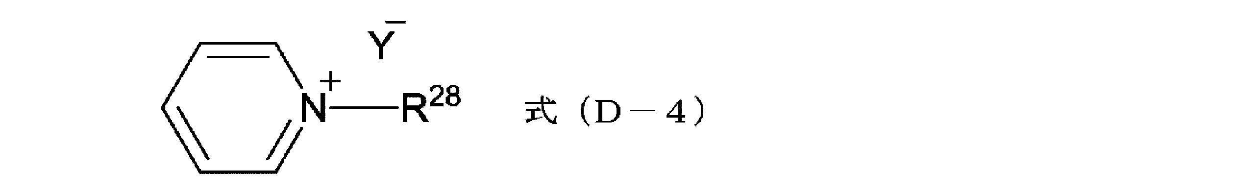
- the compound of the above formula (D-4) is a quaternary ammonium salt derived from pyridine
- R 28 is an alkyl or aryl group having 1 to 18 carbon atoms, preferably 4 to 18 carbon atoms,
- Anions (Y ⁇ ) include halogen ions such as chlorine ions (Cl ⁇ ), bromine ions (Br ⁇ ), iodine ions (I ⁇ ), carboxylates (—COO—), sulfonates (—SO 3 —),
- An acid group such as alcoholate (—O—) can be mentioned.
- this compound can be obtained as a commercial product, it is produced, for example, by reacting pyridine with an alkyl halide such as lauryl chloride, benzyl chloride, benzyl bromide, methyl bromide, octyl bromide, or an aryl halide. I can do it.
- alkyl halide such as lauryl chloride, benzyl chloride, benzyl bromide, methyl bromide, octyl bromide, or an aryl halide.
- alkyl halide such as lauryl chloride, benzyl chloride, benzyl bromide, methyl bromide, octyl bromide, or an aryl halide.
- alkyl halide such as lauryl chloride, benzyl chloride, benzyl bromide, methyl bromide, octyl bromide, or an aryl halide.
- the compound of the above formula (D-5) is a quaternary ammonium salt derived from a substituted pyridine represented by picoline and the like, and R 29 is an alkyl group having 1 to 18 carbon atoms, preferably 4 to 18 carbon atoms.
- the aryl group include a methyl group, an octyl group, a lauryl group, and a benzyl group.
- R 30 is an alkyl group having 1 to 18 carbon atoms or an aryl group. For example, in the case of quaternary ammonium derived from picoline, R 30 is a methyl group.
- Anions (Y ⁇ ) include halogen ions such as chlorine ions (Cl ⁇ ), bromine ions (Br ⁇ ), iodine ions (I ⁇ ), carboxylates (—COO—), sulfonates (—SO 3 —), An acid group such as alcoholate (—O—) can be mentioned.
- This compound can also be obtained as a commercial product. For example, a substituted pyridine such as picoline is reacted with an alkyl halide such as methyl bromide, octyl bromide, lauryl chloride, benzyl chloride or benzyl bromide, or an aryl halide. Can be manufactured. Examples of this compound include N-benzylpicolinium chloride, N-benzylpicolinium bromide, N-laurylpicolinium chloride and the like.
- the compound of the above formula (D-6) is a tertiary ammonium salt derived from an amine, m represents an integer of 2 to 11, and n represents an integer of 2 to 3.
- Anions (Y ⁇ ) include halogen ions such as chlorine ions (Cl ⁇ ), bromine ions (Br ⁇ ), iodine ions (I ⁇ ), carboxylates (—COO—), sulfonates (—SO 3 —). And acid groups such as alcoholate (—O—). It can be produced by reacting an amine with a weak acid such as carboxylic acid or phenol. Examples of the carboxylic acid include formic acid and acetic acid.
- the anion (Y ⁇ ) When formic acid is used, the anion (Y ⁇ ) is (HCOO—), and when acetic acid is used, the anion (Y ⁇ ) is (CH 3 COO). -). When phenol is used, the anion (Y ⁇ ) is (C 6 H 5 O—).
- the compound of the above formula (D-7) is a quaternary phosphonium salt having a structure of R 31 R 32 R 33 R 34 P + Y — .
- R 31 , R 32 , R 33 , and R 34 are an alkyl group or aryl group having 1 to 18 carbon atoms, or a silane compound bonded to a silicon atom through a Si—C bond, preferably R 31 to R Among the four substituents of 34 , three are phenyl groups or substituted phenyl groups, and examples thereof include phenyl groups and tolyl groups, and the remaining one is an alkyl group having 1 to 18 carbon atoms, A silane compound bonded to a silicon atom by an aryl group or Si—C bond.
- Anions (Y ⁇ ) include halogen ions such as chlorine ions (Cl ⁇ ), bromine ions (Br ⁇ ), iodine ions (I ⁇ ), carboxylates (—COO—), sulfonates (—SO 3 —). And acid groups such as alcoholate (—O—).
- This compound can be obtained as a commercial product, for example, a halogenated tetraalkylphosphonium such as tetra-n-butylphosphonium halide, tetra-n-propylphosphonium halide, or a trialkylbenzyl halide such as triethylbenzylphosphonium halide.
- Triphenylmonoalkylphosphonium halides such as phosphonium, triphenylmethylphosphonium halide, triphenylethylphosphonium halide, triphenylbenzylphosphonium halide, tetraphenylphosphonium halide, tritolylmonoarylphosphonium halide, or tritolyl monohalogenate Examples thereof include alkylphosphonium (the halogen atom is a chlorine atom or a bromine atom).
- halogens such as triphenylmonoalkylphosphonium halides such as triphenylmethylphosphonium halide, triphenylethylphosphonium halide, triphenylmonoarylphosphonium halides such as triphenylbenzylphosphonium halide, and halogens such as tritolylmonophenylphosphonium halide.
- Preferred is a tolylyl monoarylphosphonium halide, or a tolyl monoalkylphosphonium halide such as a tolyl monomethylphosphonium halide (the halogen atom is a chlorine atom or a bromine atom).
- the phosphines include methylphosphine, ethylphosphine, propylphosphine, isopropylphosphine, isobutylphosphine, phenylphosphine and other first phosphine, dimethylphosphine, diethylphosphine, diisopropylphosphine, diisoamylphosphine, diphenylphosphine and other second phosphine.
- tertiary phosphines such as trimethylphosphine, triethylphosphine, triphenylphosphine, methyldiphenylphosphine and dimethylphenylphosphine.
- the compound of the above formula (D-8) is a tertiary sulfonium salt having a structure of R 35 R 36 R 37 S + Y — .
- R 35 , R 36 , and R 37 are alkyl or aryl groups having 1 to 18 carbon atoms, or silane compounds bonded to silicon atoms through Si—C bonds, preferably 4 of R 35 to R 37 .
- Three of the substituents are phenyl groups or substituted phenyl groups, and examples thereof include phenyl groups and tolyl groups, and the remaining one is an alkyl group having 1 to 18 carbon atoms or an aryl group. It is.
- Anions (Y ⁇ ) include halogen ions such as chlorine ions (Cl ⁇ ), bromine ions (Br ⁇ ), iodine ions (I ⁇ ), carboxylates (—COO—), sulfonates (—SO 3 —). And acid groups such as alcoholate (—O—), maleate anion, and nitrate anion.
- This compound is available as a commercial product.
- halogenated tetraalkylsulfonium such as tri-n-butylsulfonium halide and tri-n-propylsulfonium halide
- trialkylbenzyl halide such as diethylbenzylsulfonium halide.
- Halogenated diphenylmonoalkylsulfonium such as sulfonium, halogenated diphenylmethylsulfonium, halogenated diphenylethylsulfonium, halogenated triphenylsulfonium, (halogen atom is chlorine or bromine atom), tri-n-butylsulfonium carboxylate, tri-n- Tetraalkylphosphonium carboxylates such as propylsulfonium carboxylate and trialkylbenzines such as diethylbenzylsulfonium carboxylate Sulfonium carboxylate, diphenylmethyl sulfonium carboxylate, diphenyl monoalkyl sulfonium carboxylate, triphenylsulfonium carboxylate such as diphenylethyl sulfonium carboxylate. Further, triphenylsulfonium halide and triphenylsulfonium carboxylate can
- a nitrogen-containing silane compound can be added as a curing catalyst.
- the nitrogen-containing silane compound include imidazole ring-containing silane compounds such as N- (3-triethoxysilylpropyl) -4,5-dihydroimidazole.
- the curing catalyst is 0.01 to 10 parts by mass, or 0.01 to 5 parts by mass, or 0.01 to 3 parts by mass with respect to 100 parts by mass of the polyorganosiloxane.
- the nitrogen-containing silane compound is particularly preferable.
- Hydrolyzable silane is hydrolyzed using a catalyst in a solvent to condense, and the resulting hydrolyzed condensate (polymer) simultaneously removes by-product alcohol, used hydrolysis catalyst, and water by distillation under reduced pressure. be able to. Moreover, the acid and base catalyst used for hydrolysis can be removed by neutralization or ion exchange.
- the stepped substrate planarization composition of the present invention may contain an organic acid, water, alcohol, or a combination thereof for stabilization of the stepped substrate planarization composition containing the hydrolysis condensate. it can.
- organic acid examples include oxalic acid, malonic acid, methylmalonic acid, succinic acid, maleic acid, malic acid, tartaric acid, phthalic acid, citric acid, glutaric acid, citric acid, lactic acid, and salicylic acid. Of these, oxalic acid and maleic acid are preferred.
- the organic acid to be added is 0.1 to 5.0 parts by mass with respect to 100 parts by mass of the condensate (polyorganosiloxane). Further, pure water, ultrapure water, ion exchange water, or the like can be used as the water to be added, and the addition amount can be 1 to 20 parts by mass with respect to 100 parts by mass of the stepped substrate planarizing composition.
- alcohol to add what is easy to be scattered by the heating after application
- coating is preferable, for example, methanol, ethanol, propanol, isopropanol, a butanol etc. are mentioned.
- the added alcohol can be 1 to 20 parts by mass with respect to 100 parts by mass of the resist underlayer film forming composition.
- the stepped substrate planarizing composition can include one or more selected from the group consisting of water, acid, and a curing catalyst.
- the step substrate flattening composition of the present invention can contain an organic polymer compound, a photoacid generator, a surfactant, and the like, if necessary, in addition to the above components.
- the dry etching rate (thickness reduction per unit time), attenuation coefficient, refractive index, etc. of the resist underlayer film formed from the stepped substrate planarizing composition of the present invention are adjusted. can do.
- Examples of the photoacid generator contained in the stepped substrate planarization composition of the present invention include onium salt compounds, sulfonimide compounds, and disulfonyldiazomethane compounds.
- Examples of onium salt compounds include diphenyliodonium hexafluorophosphate, diphenyliodonium trifluoromethanesulfonate, diphenyliodonium nonafluoronormalbutanesulfonate, diphenyliodonium perfluoronormaloctanesulfonate, diphenyliodonium camphorsulfonate, bis (4-tert-butylphenyl) iodonium camphor.
- Iodonium salt compounds such as sulfonate and bis (4-tert-butylphenyl) iodonium trifluoromethanesulfonate, and triphenylsulfonium hexafluoroantimonate, triphenylsulfonium nonafluoronormal butane sulfonate, triphenylsulfonium camphorsulfonate and triphenylsulfone Sulfonium salt compounds such as trifluoromethane sulfonate and the like.
- sulfonimide compounds include N- (trifluoromethanesulfonyloxy) succinimide, N- (nonafluoronormalbutanesulfonyloxy) succinimide, N- (camphorsulfonyloxy) succinimide and N- (trifluoromethanesulfonyloxy) naphthalimide. Can be mentioned.
- disulfonyldiazomethane compound examples include bis (trifluoromethylsulfonyl) diazomethane, bis (cyclohexylsulfonyl) diazomethane, bis (phenylsulfonyl) diazomethane, bis (p-toluenesulfonyl) diazomethane, and bis (2,4-dimethylbenzenesulfonyl). And diazomethane, and methylsulfonyl-p-toluenesulfonyldiazomethane.
- the ratio is 0.01 to 15 parts by mass, or 0.1 to 10 parts by mass, or 0.5 with respect to 100 parts by mass of the condensate (polyorganosiloxane). ⁇ 1 part by mass.
- the surfactant is effective in suppressing the occurrence of pinholes and installations when the stepped substrate planarizing composition of the present invention is applied to the substrate.
- the surfactant contained in the stepped substrate planarizing composition of the present invention include polyoxyethylene alkyl such as polyoxyethylene lauryl ether, polyoxyethylene stearyl ether, polyoxyethylene cetyl ether, and polyoxyethylene oleyl ether.
- Ethers polyoxyethylene octylphenol ether, polyoxyethylene alkylallyl ethers such as polyoxyethylene nonylphenol ether, polyoxyethylene / polyoxypropylene block copolymers, sorbitan monolaurate, sorbitan monopalmitate, sorbitan monostearate Sorbitan monooleate, sorbitan trioleate, sorbitan fatty acid esters such as sorbitan tristearate, polyoxyethylene sorbate Nonionic surfactants such as polyoxyethylene sorbitan fatty acid esters such as polymonoethylene lauritan, polyoxyethylene sorbitan monopalmitate, polyoxyethylene sorbitan monostearate, polyoxyethylene sorbitan trioleate, polyoxyethylene sorbitan tristearate Agents, trade names F-top EF301, EF303, EF352 (manufactured by Tochem Products Co., Ltd.), trade names MegaFuck F171, F173, R-08, R-30, R
- surfactants may be used alone or in combination of two or more.
- the ratio is 0.0001 to 5 parts by mass, or 0.001 to 1 part by mass, or 0.01 to 1 with respect to 100 parts by mass of the condensate (polyorganosiloxane). Part by mass.
- a rheology adjusting agent, an adhesion aid and the like can be added to the stepped substrate planarizing composition of the present invention.
- the rheology modifier is effective for improving the fluidity of the underlayer film forming composition.
- the adhesion aid is effective for improving the adhesion between the semiconductor substrate or resist and the lower layer film.
- any solvent can be used without particular limitation as long as it can dissolve the solid content.
- solvents include methyl cellosolve acetate, ethyl cellosolve acetate, propylene glycol, propylene glycol monomethyl ether, propylene glycol monoethyl ether, methyl isobutyl carbinol, propylene glycol monobutyl ether, propylene glycol monomethyl ether acetate, propylene glycol mono Ether ether acetate, propylene glycol monopropyl ether acetate, propylene glycol monobutyl ether acetate, toluene, xylene, methyl ethyl ketone, cyclopentanone, cyclohexanone, ethyl 2-hydroxypropionate, ethyl 2-hydroxy-2-methylpropionate, ethyl ethoxyacetate , Ethyl
- step difference board a silicon wafer having a step formed by the Bosch method or alkaline water and having this step on one side
- the method for producing a semiconductor device including the method for planarizing a semiconductor substrate according to the present invention comprises a step (1) of forming an organic pattern on the substrate, and the composition according to any one of claims 1 to 7 in the organic pattern.
- a method for manufacturing a semiconductor device comprising a step (3) of applying, and a step (4) of removing the organic pattern by etching to reverse the pattern.
- the organic pattern is a photoresist pattern, a resist underlayer film (coating type or vapor deposition type) pattern that functions as an etching mask for the lower semiconductor substrate, and a pattern formed by nanoimprint.
- the method for manufacturing a semiconductor device including the method for planarizing a semiconductor substrate of the present invention includes, for example, a step of applying a resist on the substrate (1a), a step of exposing and developing the resist (2), and a resist during or after development.
- a method for manufacturing a semiconductor device includes a step (3a) of applying a coating polysiloxane composition according to the present invention to a pattern, and a step (4a) of removing the resist pattern by etching to reverse the pattern.
- the photoresist used in the step (1a) is not particularly limited as long as it is sensitive to light used for exposure. Either a negative photoresist or a positive photoresist can be used.
- a positive photoresist comprising a novolac resin and 1,2-naphthoquinonediazide sulfonic acid ester, a chemically amplified photoresist comprising a binder having a group that decomposes with an acid to increase the alkali dissolution rate and a photoacid generator, an acid
- a chemically amplified photoresist comprising a low-molecular compound that decomposes to increase the alkali dissolution rate of the photoresist, an alkali-soluble binder, and a photoacid generator, and a binder having a group that decomposes with an acid to increase the alkali dissolution rate
- Examples include trade name APEX-E manufactured by Shipley, trade name PAR710 manufactured by Sumitomo Chemical Co., Ltd., and trade name SEPR430 manufactured by Shin-Etsu Chemical Co., Ltd. Also, for example, Proc. SPIE, Vol. 3999, 330-334 (2000), Proc. SPIE, Vol. 3999, 357-364 (2000), Proc. SPIE, Vol. 3999, 365-374 (2000), and fluorine-containing polymer-based photoresists.
- Chemically amplified resist comprising a binder having a group that decomposes with an acid generator and an acid to change the alkali dissolution rate, a low molecular weight compound that decomposes with an alkali-soluble binder, an acid generator and an acid to change the alkali dissolution rate of the resist
- a chemically amplified resist comprising: a binder having a group that decomposes with an acid generator and an acid to change the alkali dissolution rate; and a chemically amplified resist comprising a low-molecular compound that decomposes with an acid to change the alkali dissolution rate of the resist,
- non-chemically amplified resists composed of a binder having a group that changes the alkali dissolution rate by being decomposed by an electron beam and non-chemically amplified resists composed of a binder having a portion that is cut by an electron beam to change the alkali dis
- the resist solution is applied and then subjected to a baking temperature of 70 to 150 ° C. and a baking time of 0.5 to 5 minutes.
- the resist film thickness is obtained in the range of 10 to 1000 nm.
- the resist solution, the developer, and the coating materials shown below can be coated by spin coating, dipping, spraying, or the like, but the spin coating method is particularly preferable.
- the resist is exposed through a predetermined mask.
- a KrF excimer laser (wavelength 248 nm), an ArF excimer laser (wavelength 193 nm), EUV light (wavelength 13.5 nm), an electron beam, or the like can be used.
- post-exposure heating PEB: Post Exposure Bake
- the post-exposure heating is appropriately selected from a heating temperature of 70 ° C. to 150 ° C. and a heating time of 0.3 to 10 minutes.
- a step (1a-1) of forming a resist underlayer film on the substrate may be included before the step (1) or (1a).
- the resist underlayer film has antireflection and organic hard mask functions.
- the formation of the resist in the step (1a) can be performed by a step (1a) in which a resist underlayer film is formed on the semiconductor substrate and a resist is formed thereon.
- a resist underlayer film can be formed on the semiconductor substrate, a silicon hard mask can be formed thereon, and a resist can be formed thereon.
- the resist underlayer film used in the above step (1a-1) prevents irregular reflection during exposure of the upper layer resist, and is used for the purpose of improving adhesion with the resist.
- an acrylic resin or the like A novolac resin can be used.
- the resist underlayer film can form a film having a thickness of 1 to 1,000 nm on the semiconductor substrate.
- the resist underlayer film used in the above step (1a-1) is a hard mask using an organic resin, and a material having a high carbon content and a low hydrogen content is used.
- a material having a high carbon content and a low hydrogen content is used.
- polyvinyl naphthalene resin, carbazole novolak resin, phenol novolak resin, naphthol novolak resin, and the like can be given. These can form a film with a film thickness of 5 to 1,000 nm on a semiconductor substrate.
- As the silicon hard mask used in the above step (1a-1) polysiloxane obtained by hydrolyzing hydrolyzable silane can be used.
- polysiloxane obtained by hydrolyzing tetraethoxysilane, methyltrimethoxysilane, and phenyltriethoxysilane can be exemplified. These can form a film with a film thickness of 5 to 200 nm on the resist underlayer film.
- Step (2) exposure is performed through a predetermined mask.
- a KrF excimer laser (wavelength 248 nm), an ArF excimer laser (wavelength 193 nm), EUV (wavelength 13.5 nm), or the like can be used.
- post-exposure bake can be performed as necessary.
- the post-exposure heating is performed under conditions appropriately selected from a heating temperature of 70 ° C. to 150 ° C. and a heating time of 0.3 to 10 minutes.
- development is performed with a developer.
- a developer for example, when a positive photoresist is used, the exposed portion of the photoresist is removed, and a photoresist pattern is formed.
- Developers include aqueous solutions of alkali metal hydroxides such as potassium hydroxide and sodium hydroxide, aqueous solutions of quaternary ammonium hydroxides such as tetramethylammonium hydroxide, tetraethylammonium hydroxide and choline, ethanolamine, propylamine, An alkaline aqueous solution such as an aqueous amine solution such as ethylenediamine can be mentioned as an example. Further, a surfactant or the like can be added to these developers.
- the development conditions are appropriately selected from a temperature of 5 to 50 ° C. and a time of 10 to 600 seconds.
- an organic solvent can be used as the developer.
- development is performed with a developer (solvent). As a result, for example, when a positive photoresist is used, the unexposed portion of the photoresist is removed, and a photoresist pattern is formed.
- Developers include, for example, methyl acetate, butyl acetate, ethyl acetate, isopropyl acetate, amyl acetate, isoamyl acetate, ethyl methoxyacetate, ethyl ethoxy acetate, propylene glycol monomethyl ether acetate, ethylene glycol monoethyl ether acetate, ethylene glycol monopropyl Ether acetate, ethylene glycol monobutyl ether acetate, ethylene glycol monophenyl ether acetate, diethylene glycol monomethyl ether acetate, diethylene glycol monopropyl ether acetate, diethylene glycol monoethyl ether acetate, diethylene glycol monophenyl ether acetate, diethylene glycol monobutyl ether acetate, diethylene glycol Monoethyl ether acetate, 2-methoxybutyl acetate, 3-methoxybutyl acetate,
- Step (3) the step-substrate flattening composition according to the present invention is applied to the resist during or after development and baked to produce a polysiloxane coating film, whereby the pattern between the resist patterns is formed.
- a polysiloxane composition film embedded with the composition is formed.
- the applied stepped substrate planarizing composition is fired at a heating temperature of 50 to 180 ° C. for 0.5 to 5 minutes.
- the iso-dense bias of the polysiloxane coating film is 50 nm or less.
- the iso-dense bias of the polysiloxane coating film refers to the shortest part and the largest part of the length from the interface on the side of the stepped substrate contacting the film to the interface on the side of the polysiloxane coating film in contact with the atmosphere.
- the length of b expressed below is the Iso-dense bias.
- a is the recess depth of the polysiloxane coating film at the center of the dense space portion
- b is the recess depth of the polysiloxane coating film at the center of the open space portion
- c is used.
- the depth of the initial space in the stepped substrate, d is a polysiloxane coating film, and e is the stepped substrate.
- the stepped substrate can be an organic pattern (photoresist pattern, resist underlayer film (coating or vapor deposition type) pattern functioning as an etching mask for the lower semiconductor substrate, a pattern formed by nanoimprinting, etc.).
- the first coating polysiloxane composition containing the first coating polysiloxane is applied and baked to produce a first polysiloxane coating film.
- the pattern between the resists is separated.
- a polysiloxane composition film embedded with the composition can also be formed. This mode is shown in FIGS. 5 (3) and (4).
- the second coating polysiloxane composition should be the stepped substrate planarizing composition according to the present invention, but the first coating polysiloxane composition should be any known polysiloxane composition as appropriate. You can select and use.
- the applied coating polysiloxane composition is fired at a heating temperature of 50 to 180 ° C. for 0.5 to 5 minutes, respectively.
- the iso-dense bias of the second polysiloxane coating film is 50 nm or less.
- a step (3-1) of exposing the surface of the organic pattern (for example, resist pattern) by etching back the surface of the coating film can be included.
- the resist pattern surface and the coating composition surface coincide with each other, and only the resist component is removed from the difference in the gas etching rate between the resist pattern and the coating composition. Will remain, resulting in pattern inversion.
- the resist pattern is exposed by a gas (for example, a fluorine-based gas) that can remove the coating composition.
- step (4) the resist pattern is removed by etching to reverse the pattern.
- dry etching is performed using tetrafluoromethane, perfluorocyclobutane (C 4 F 8 ), perfluoropropane (C 3 F 8 ), trifluoromethane, carbon monoxide, argon, oxygen, nitrogen, sulfur hexafluoride. , Gas such as difluoromethane, nitrogen trifluoride and chlorine trifluoride.
- dry etching is preferably performed with an oxygen-based gas.
- a reverse pattern (reversal pattern) is formed by the polymer for pattern reversal formation (polysiloxane obtained by hydrolyzing and condensing hydrolyzable silane) contained in the coating composition.
- reaction solution is cooled to room temperature, 19 g of propylene glycol monomethyl ether acetate is added to the reaction solution, and acetone, water, acetic acid, and ethanol as a reaction byproduct are distilled off from the reaction solution under reduced pressure and concentrated to obtain a cohydrolyzate.
- a propylene glycol monomethyl ether acetate solution of the decomposition condensate (polymer) was obtained.
- the solid content concentration was adjusted to 30% by mass in terms of solid residue at 140 ° C.
- 15 g of the prepared polymer solution was transferred to a 100 ml flask and reacted in an oil bath adjusted to 100 ° C. for 12 hours.
- the weight average molecular weight Mw by GPC was 10,000 in terms of polystyrene.
- reaction solution was cooled to room temperature and transferred to a 500 ml separatory funnel.
- separatory funnel To the separatory funnel were added 100 g of ethyl acetate, 34 g of 6N hydrochloric acid, and 68 g of ultrapure water, and a liquid separation operation was performed to obtain an ethyl acetate layer.
- 68 g of ultrapure water was added for washing. The washing operation was further repeated once, and the resulting ethyl acetate layer was concentrated under reduced pressure using an evaporator.
- the solid content concentration of the obtained hydrolyzed condensate (polymer) in the ethyl acetate solution was adjusted to 20% by mass in terms of solid residue at 140 ° C.
- the weight average molecular weight Mw by GPC was 4,000 in terms of polystyrene.
- reaction solution is cooled to room temperature, 100 g of 4-methyl-2-pentanol is added to the reaction solution, and acetone, water, hydrochloric acid, and ethanol as a reaction byproduct are distilled off from the reaction solution under reduced pressure and concentrated.
- a 4-methyl-2-pentanol solution of the cohydrolyzed condensate (polymer) was obtained. Solid content concentration was adjusted so that it might become 13 mass% in conversion of the solid residue in 140 degreeC.
- the weight average molecular weight Mw by GPC was 1,400 in terms of polystyrene.
- the silanol group ratio in the polymer was calculated by 1 H NMR. The measurement was performed using JNM-ECA500 (manufactured by JEOL). First, when the integration ratio of the chemical shift values (0.0-0.6 ppm) of methyl protons of triethoxymethylsilane or dimethyldiethoxysilane is taken as a reference, the silanol group is detected as a broad peak at 5-7 ppm. . By comparing the integration ratio of 5-7 ppm, the ratio (mol%) of silanol groups to one Si atom in the polymer was calculated.
- a chemical shift derived from a silane monomer structure other than silanol groups may be detected at 5-7 ppm, so that many silanol groups may be detected apparently. Since the compounding ratio of triethoxymethylsilane or dimethyldiethoxysilane to other constituent silane monomers is already existing, it is detected at 5-7ppm of constituent silane monomers from the integral ratio of triethoxymethylsilane or dimethyldiethoxysilane methyl protons. The integration ratio of the monomer-derived peaks can be estimated.
- the net silanol amount was calculated by subtracting the integral ratio of the constituent silane monomers as described above.
- the amount of silanol of each synthesis example polymer calculated by the above method and a commercially available polysilsesquioxane resin (product name: SR-13H (manufactured by Konishi Chemical, Example A3)) was as follows. (Preparation of coating solution) Each of the polymers obtained in Synthesis Examples A1 and A2 and Comparative Synthesis Example A1 and SR-13H was mixed with an acid, a curing catalyst, a solvent, and ultrapure water in the proportions shown in Table 1, to form a coating film forming composition.
- the addition ratio of the polymer in Table 1 indicates not the addition amount of the polymer solution but the addition amount of the polymer itself.
- maleic acid is MA
- N- (3-triethoxysilylpropyl) -4,5-dihydroimidazole is IMIDTEOS
- 4-methyl-2-pentanol is MIBC
- propylene glycol monomethyl ether acetate is PGMEA
- propylene glycol Monoethyl ether was abbreviated as PGEE
- propylene glycol monomethyl ether as PGME
- ultrapure water DIW.
- Each addition amount was shown in parts by mass.
- the thickness of the polysiloxane coating film was 90 nm. Subsequently, about the obtained polysiloxane coating film, the cross-sectional shape was observed by cross-sectional SEM, and planarization property was evaluated. A groove pattern having a depth of 220 nm and a width of 800 nm is observed, and the film thickness (that is, the length from the interface on the side in contact with the silicon substrate film to the interface on the side in contact with the air of the polysiloxane coating film) is measured with respect to the groove bottom. The film thickness difference between the smallest part and the largest part was measured and the film thickness difference was calculated. The smaller the film thickness difference, the better the flatness.
- the SEM photographs used for the evaluation are shown in FIGS.
Landscapes
- Chemical & Material Sciences (AREA)
- Physics & Mathematics (AREA)
- General Physics & Mathematics (AREA)
- Chemical Kinetics & Catalysis (AREA)
- Organic Chemistry (AREA)
- Engineering & Computer Science (AREA)
- Health & Medical Sciences (AREA)
- Polymers & Plastics (AREA)
- Medicinal Chemistry (AREA)
- Materials Engineering (AREA)
- Wood Science & Technology (AREA)
- Life Sciences & Earth Sciences (AREA)
- Architecture (AREA)
- Structural Engineering (AREA)
- Spectroscopy & Molecular Physics (AREA)
- Silicon Polymers (AREA)
- Photosensitive Polymer And Photoresist Processing (AREA)
- Paints Or Removers (AREA)
- Materials For Photolithography (AREA)
Abstract
Description
[1] 加水分解性シラン原料の加水分解縮合物を含むポリシロキサンと溶媒とを含む、有機パターン上に塗布される有機パターン平坦化用組成物であって、
上記ポリシロキサンが、Si原子に対し、シラノール基を20モル%以下の割合で含むものであり、
上記ポリシロキサンの重量平均分子量が1,000~50,000である、該組成物。
[2] 上記ポリシロキサンが、式(1):

(式(1)中、R1はアルキル基、アリール基、ハロゲン化アルキル基、ハロゲン化アリール基、アルコキシアリール基、アルケニル基、又はエポキシ基、アクリロイル基、メタクリロイル基、メルカプト基、もしくはシアノ基を有する有機基で且つSi-C結合によりケイ素原子と結合しているものであり、R2はアルコキシ基、アシルオキシ基、又はハロゲン基を示し、aは1を示す。)で示される加水分解性シランを含む加水分解性シラン原料の加水分解縮合物を含む、[1]に記載の組成物。
[3] 上記ポリシロキサンが、上記式(1)で示され、aが1である加水分解性シランを100~50モル%、好ましくは95~50モル%、及び上記式(1)で示され、aが2である加水分解性シランを0~50モル%、好ましくは5~50モル%となる割合で含む加水分解性シラン原料の加水分解縮合物を含む、[2]に記載の組成物。
[4] 上記ポリシロキサンが、上記式(1)のaが0の加水分解性シランを0~100モル%、好ましくは1~100モル%、及びaが1である加水分解性シランを0~100モル%、好ましくは0~99モル%となる割合で含む加水分解性シラン原料の加水分解縮合物のアルコール及び酸による脱水処理生成物である、[2]又は[3]に記載の組成物。
[5] 上記ポリシロキサンが、上記式(1)のaが1又は2の加水分解性シラン原料の加水分解縮合物の非アルコールと弱酸又は塩基とによる処理生成物である、[2]又は[3]にいずれか1項に記載の組成物。
[6] 弱酸が4~5の酸解離定数を有する酸である、[5]に記載の組成物。
[7] 上記有機パターンがレジストパターン、ナノインプリントパターン及び有機下層膜パターンの中から選ばれる、[1]~[6]のいずれか1項に記載の組成物。
[8] 基板上に有機パターンを形成する工程(1)、有機パターンに[1]~[7]のいずれか1項に記載の組成物を塗布する工程(3)、有機パターンをエッチング除去してパターンを反転させる工程(4)、を含む半導体装置の製造方法。
[9] 基板上にレジストを形成する工程(1a)、レジストを露光と現像する工程(2)、現像中又は現像後のレジストパターンに[1]~[7]のいずれか1項に記載の組成物を塗布する工程(3a)、レジストパターンをエッチング除去してパターンを反転させる工程(4a)、を含む半導体装置の製造方法。
[10] 工程(1a)の前に、基板上にレジスト下層膜を形成する工程(1a-1)を含む、[9]に記載の製造方法。
[11] 工程(3)の後に、塗膜表面をエッチバックして有機パターン表面を露出する工程(3-1)を含む、[8]に記載の製造方法。
[12] 有機パターンに塗布される段差基板平坦化用組成物に含まれるポリシロキサンの製造方法であって、
式(1):

(式(1)中、R1はアルキル基、アリール基、ハロゲン化アルキル基、ハロゲン化アリール基、アルコキシアリール基、アルケニル基、又はエポキシ基、アクリロイル基、メタクリロイル基、メルカプト基、もしくはシアノ基を有する有機基で且つSi-C結合によりケイ素原子と結合しているものであり、R2はアルコキシ基、アシルオキシ基、又はハロゲン基を示し、aは0を示す。)で示され、aが0の加水分解性シランを0~100モル%、好ましくは1~100モル%、及び式(1)で示され、aが1である加水分解性シランを0~100モル%、好ましくは0~99モル%となる割合で含む加水分解性シラン原料の加水分解縮合物を、アルコールと酸で脱水処理する工程を含む、製造方法。
[13] 有機パターンに塗布される段差基板平坦化用組成物に含まれるポリシロキサンの製造方法であって、
式(1):

(式(1)中、R1はアルキル基、アリール基、ハロゲン化アルキル基、ハロゲン化アリール基、アルコキシアリール基、アルケニル基、又はエポキシ基、アクリロイル基、メタクリロイル基、メルカプト基、もしくはシアノ基を有する有機基で且つSi-C結合によりケイ素原子と結合しているものであり、R2はアルコキシ基、アシルオキシ基、又はハロゲン基を示し、aは1又は2を示す。)で示され、aが1又は2の加水分解性シラン原料の加水分解縮合物を、非アルコールと弱酸又は塩基とで処理する工程を含む、製造方法。
本発明に係る段差基板平坦化用組成物について以下に説明する。
上記ポリシロキサン中のシラノール基比率は1H NMRにて算出できる。

(式(1)中、R1はアルキル基、アリール基、ハロゲン化アルキル基、ハロゲン化アリール基、アルコキシアリール基、アルケニル基、又はエポキシ基、アクリロイル基、メタクリロイル基、メルカプト基、もしくはシアノ基を有する有機基で且つSi-C結合によりケイ素原子と結合しているものであり、R2はアルコキシ基、アシルオキシ基、又はハロゲン基を示し、aは1を示す。)で示される加水分解性シランを含む加水分解性シラン原料の加水分解縮合物を含む。
さらに好ましくは、式(1)中aが1である加水分解性シランを95~70モル%及び、式(1)中aが2である加水分解性シランを5~30モル%となる割合で含む。
また、酸は、70~160℃の沸点を有する酸が好ましい。例えば、トリフルオロ酢酸、イソ酪酸、酢酸等が挙げられる。
上記の酸は、酸解離定数(pka)が4~5であるか、又は沸点が70~160℃であるか、いずれかの物性を有するものが好ましい。即ち、酸性度が弱いものか、又は酸性度は強くても沸点が低いものを用いることができる。
そして、酸としては酸解離定数、沸点の性質からいずれの性質を利用することも可能であるが、両方の性質を持つ酢酸は好ましく用いることができる。
本発明ではレジストの露光後に用いられる塗布用組成物であるため、マスクを通じてレジストの露光し現像中又は現像後に上記組成物で充填される。
これにより後のドライエッチング工程で、ガス種の選定により、レジストを選択的にドライエッチング除去して充填した加水分解縮合物(ポリシロキサン)による新たなパターンが形成される。

段差基板平坦化用組成物に含まれていても良いその他の成分について以下に説明する。

(但し、mは2~11、nは2~3の整数を、R21はアルキル基又はアリール基を、Y-は陰イオンを示す。)で示される構造を有する第4級アンモニウム塩、
式(D-2):

(但し、R22、R23、R24及びR25はアルキル基又はアリール基を、Nは窒素原子を、Y-は陰イオンを示し、且つR22、R23、R24、及びR25はそれぞれC-N結合により窒素原子と結合されているものである)で示される構造を有する第4級アンモニウム塩、
式(D-3):

(但し、R26及びR27はアルキル基又はアリール基を、Y-は陰イオンを示す)の構造を有する第4級アンモニウム塩、
式(D-4):
(但し、R28はアルキル基又はアリール基を、Y-は陰イオンを示す)の構造を有する第4級アンモニウム塩、
式(D-5):

(但し、R29及びR30はアルキル基又はアリール基を、Y-は陰イオンを示す)の構造を有する第4級アンモニウム塩、
式(D-6):

(但し、mは2~11、nは2~3の整数を、Hは水素原子を、Y-は陰イオンを示す)の構造を有する第3級アンモニウム塩が上げられる。
(但し、R31、R32、R33、及びR34はアルキル基又はアリール基を、Pはリン原子を、Y-は陰イオンを示し、且つR31、R32、R33、及びR34はそれぞれC-P結合によりリン原子と結合されているものである)で示される第4級ホスホニウム塩が上げられる。
(但し、R35、R36、及びR37はアルキル基又はアリール基を、Sは硫黄原子を、Y-は陰イオンを示し、且つR35、R36、及びR37はそれぞれC-S結合により硫黄原子と結合されているものである)で示される第3級スルホニウム塩が上げられる。
以下本発明の半導体基板の平坦化方法を含む半導体装置の製造方法の一例を以下に説明する。また、概要を図5に示す。
なお、本発明にいう段差基板としては、MEMSデバイス向けのウエハが挙げられる。例えば、(1b)ボッシュ法もしくはアルカリ水により段差が形成されたシリコンウエハで、片面にこの段差を有するもの、(2b)同様にシリコンウエハとシリコンウエハの間にシリコン酸化膜が存在しるSOI(Silicon on Insulator)ウエハで、片面段差を有するもの、(3b)ガリウムヒ素基板で、片面に段差形状を有するもの、(4b)シリコンウエハ上に金属・絶縁膜が形成されていて、片面に段差形状を有するものなどが例示される。
上記有機パターンは、フォトレジストパターン、下層半導体基板のエッチングマスクとして機能するレジスト下層膜(塗布型又は蒸着型)パターン、ナノインプリントにて形成されたパターンである。
工程(1a)に用いられるフォトレジストとしては露光に使用される光に感光するものであれば特に限定はない。ネガ型フォトレジスト及びポジ型フォトレジストのいずれも使用できる。ノボラック樹脂と1,2-ナフトキノンジアジドスルホン酸エステルとからなるポジ型フォトレジスト、酸により分解してアルカリ溶解速度を上昇させる基を有するバインダーと光酸発生剤からなる化学増幅型フォトレジスト、酸により分解してフォトレジストのアルカリ溶解速度を上昇させる低分子化合物とアルカリ可溶性バインダーと光酸発生剤とからなる化学増幅型フォトレジスト、及び酸により分解してアルカリ溶解速度を上昇させる基を有するバインダーと酸により分解してフォトレジストのアルカリ溶解速度を上昇させる低分子化合物と光酸発生剤からなる化学増幅型フォトレジストなどがある。例えば、シプレー社製商品名APEX-E、住友化学工業(株)製商品名PAR710、及び信越化学工業(株)製商品名SEPR430等が挙げられる。また、例えば、Proc.SPIE,Vol.3999,330-334(2000)、Proc.SPIE,Vol.3999,357-364(2000)、やProc.SPIE,Vol.3999,365-374(2000)に記載されているような、含フッ素原子ポリマー系フォトレジストを挙げることができる。
工程(2)において、所定のマスクを通して露光が行なわれる。露光には、KrFエキシマレーザー(波長248nm)、ArFエキシマレーザー(波長193nm)及びEUV(波長13.5nm)等を使用することができる。露光後、必要に応じて露光後加熱(post exposure bake)を行なうこともできる。露光後加熱は、加熱温度70℃~150℃、加熱時間0.3~10分間から適宜、選択された条件で行われる。次いで、現像液によって現像が行なわれる。これにより、例えばポジ型フォトレジストが使用された場合は、露光された部分のフォトレジストが除去され、フォトレジストのパターンが形成される。
工程(3)として、現像中又は現像後のレジストに、本発明に係る段差基板平坦化用組成物を塗布・焼成してポリシロキサン被覆膜を作製することにより、該レジストのパターン間を該組成物で埋め込んだポリシロキサン組成物膜を形成する。塗布された段差基板平坦化用組成物の焼成は加熱温度50~180℃で0.5~5分間行われる。ポリシロキサン被覆膜のIso-denseバイアスは50nm以下とする。なお、ポリシロキサン被覆膜のIso-denseバイアスとは、上記段差基板の膜と接する側の界面からポリシロキサン被覆膜の大気と接する側の界面までの長さの最も小さい箇所と最も大きい箇所との膜厚差をいう。具体的には、以下で表されるbの長さがIso-denseバイアスである。図中、aは密のスペース部の中心でのポリシロキサン被覆膜の凹み深さであり、bはオープンスペース部の中心でのポリシロキサン被覆膜の凹み深さであり、cは使用した段差基板における当初のスペースの深さであり、 dはポリシロキサン被覆膜であり、eは段差基板である。段差基板は有機パターン(フォトレジストパターン、下層半導体基板のエッチングマスクとして機能するレジスト下層膜(塗布型又は蒸着型)パターン、ナノインプリントにて形成されたパターン等)基板とすることができる。
また、本工程において、第一被覆用ポリシロキサンを含む第一被覆用ポリシロキサン組成物を塗布・焼成して第一ポリシロキサン被覆膜を作製し、第一ポリシロキサン被覆膜の上に、第一被覆用ポリシロキサンとは異なる第二被覆用ポリシロキサンを含む第二被覆用ポリシロキサン組成物を塗布・焼成して第二ポリシロキサン被覆膜を作製することにより、該レジストのパターン間を該組成物で埋め込んだポリシロキサン組成物膜を形成することもできる。図5(3)、(4)にはこの態様を示した。この場合、少なくとも第二被覆用ポリシロキサン組成物は本発明に係る段差基板平坦化用組成物とすべきであるが、第一被覆用ポリシロキサン組成物は公知の任意のポリシロキサン組成物を適宜選択して使用することができる。塗布された被覆用ポリシロキサン組成物の焼成はそれぞれ、加熱温度50~180℃で0.5~5分間行われる。第二ポリシロキサン被覆膜のIso-denseバイアスは50nm以下とする。
工程(4)ではレジストパターンをエッチング除去してパターンを反転させる。工程(4)において、ドライエッチングはテトラフルオロメタン、パーフルオロシクロブタン(C4F8)、パーフルオロプロパン(C3F8)、トリフルオロメタン、一酸化炭素、アルゴン、酸素、窒素、六フッ化硫黄、ジフルオロメタン、三フッ化窒素及び三フッ化塩素等のガスを用いて行われる。特に酸素系のガスによりドライエッチングが行われることが好ましい。
ビニルトリメトキシシラン30.0g(80mol%)、ジメチルジエトキシシラン7.5g(20mol%)およびプロピレングリコールモノメチルエーテルアセテート56gを300mlのフラスコに入れ、そのフラスコ内の混合溶液をマグネチックスターラーにて撹拌しながら、0.01mol/Lの酢酸16.4gをその混合溶液に滴下した。滴下後、95℃に調整されたオイルバスにフラスコを移し、24時間反応させた。その後、反応溶液を室温まで冷却し、その反応溶液にプロピレングリコールモノメチルエーテルアセテートを19g加え、アセトン、水及び酢酸、並びに反応副生物であるエタノールを反応溶液から減圧留去し濃縮して、共加水分解縮合物(ポリマー)のプロピレングリコールモノメチルエーテルアセテート溶液を得た。固形分濃度は140℃における固形残物換算で30質量%となるように調整した。
作成したポリマー溶液15gを100mlフラスコに移し、100℃に調整されたオイルバス中で12時間反応させた。GPCによる重量平均分子量Mwはポリスチレン換算で10,000であった。
35質量%のテトラエチルアンモニウムヒドロキシド水溶液17.0g、2-プロパノール27.4g、テトラヒドロフラン54.8gを200mlナスフラスコに入れ、そのフラスコ内の混合溶液をマグネチックスターラーにて撹拌しながら、ビニルトリメトキシシラン9.0g(30mol%)、メチルトリエトキシシラン25.3g(70mol%)を滴下した。滴下後、85℃に調整されたオイルバスにフラスコを移し、加温還流下で4時間反応させた。その後、反応溶液を室温まで冷却して500mlの分液ロートに移した。分液ロートに酢酸エチル100g、6規定塩酸34g、超純水68gを加え、分液操作を行い、酢酸エチル層を得た。得られた酢酸エチル層に68gの超純水を加え、洗浄を行った。洗浄操作をさらに1度繰り返し、得られた酢酸エチル層をエバポレーターにより減圧濃縮した。得られた加水分解縮合物(ポリマー)の酢酸エチル溶液の固形分濃度は140℃における固形残物換算で20質量%となるように調整した。GPCによる重量平均分子量Mwはポリスチレン換算で4,000であった。
テトラエトキシシラン53.9g(50mol%)、メチルトリエトキシシラン46.1g(50mol%)およびアセトン100gを500mlのフラスコに入れ、そのフラスコ内の混合溶液をマグネチックスターラーにて撹拌しながら、0.01mol/Lの塩酸32.6gをその混合溶液に滴下した。滴下後、85℃に調整されたオイルバスにフラスコを移し、加温還流下で4時間反応させた。その後、反応溶液を室温まで冷却し、その反応溶液に4-メチル-2-ペンタノールを100g加え、アセトン、水及び塩酸、並びに反応副生物であるエタノールを反応溶液から減圧留去し濃縮して、共加水分解縮合物(ポリマー)の4-メチル-2-ペンタノール溶液を得た。固形分濃度は140℃における固形残物換算で13質量%となるように調整した。GPCによる重量平均分子量Mwはポリスチレン換算で1,400であった。
ポリマー中のシラノール基比率は1H NMRにて算出した。測定はJNM-ECA500(JEOL製)を用いて行った。まずトリエトキシメチルシランまたはジメチルジエトキシシランのメチルプロトンの化学シフト値(0.0-0.6ppm)の積分比を取り基準とした場合、シラノール基は5-7ppmでブロードなピークとして検出される。この5-7ppmの積分比を比較することで、ポリマー中のSi原子1個に対するシラノール基の比率(モル%)を算出した。
また一部ポリマーによっては5-7ppmにシラノール基以外のシランモノマー構造に由来する化学シフトが検出されてしまうことがあるため、見かけ上、シラノール基が多く検出されてしまうことがある。トリエトキシメチルシランまたはジメチルジエトキシシランとその他の構成シランモノマーの配合比率が既存であるため、トリエトキシメチルシランまたはジメチルジエトキシシランメチルプロトンの積分比から、構成シランモノマーの5-7ppmで検出されるモノマー由来ピークの積分比を見積もることができる。シラノール基と同一の化学シフトの範囲に化学シフトを持つシランモノマーを加える場合は、上記のようにして構成シランモノマーの積分比分を差し引くことで正味のシラノール量を算出した。
上記方法で算出された各合成例ポリマーおよび市販のポリシルセスキオキサン樹脂(製品名:SR―13H(小西化学製, 実施例A3))のシラノール量は下記のようになった。

〔塗布液の調製〕
上記合成例A1、A2及び比較合成例A1で得られたポリマー並びに上記SR―13Hの各々と、酸、硬化触媒、溶媒、超純水とを表1に示す割合で混合し、塗布膜形成組成物をそれぞれ調製した。表1中のポリマーの添加割合はポリマー溶液の添加量ではなく、ポリマー自体の添加量を示した。表1中でマレイン酸はMA、N-(3-トリエトキシシリプロピル)-4,5-ジヒドロイミダゾールはIMIDTEOS、4-メチル-2-ペンタノールはMIBC、プロピレングリコールモノメチルエーテルアセテートはPGMEA、プロピレングリコールモノエチルエーテルはPGEE、プロピレングリコールモノメチルエーテルはPGME、超純水はDIWと略した。各添加量は質量部で示した。
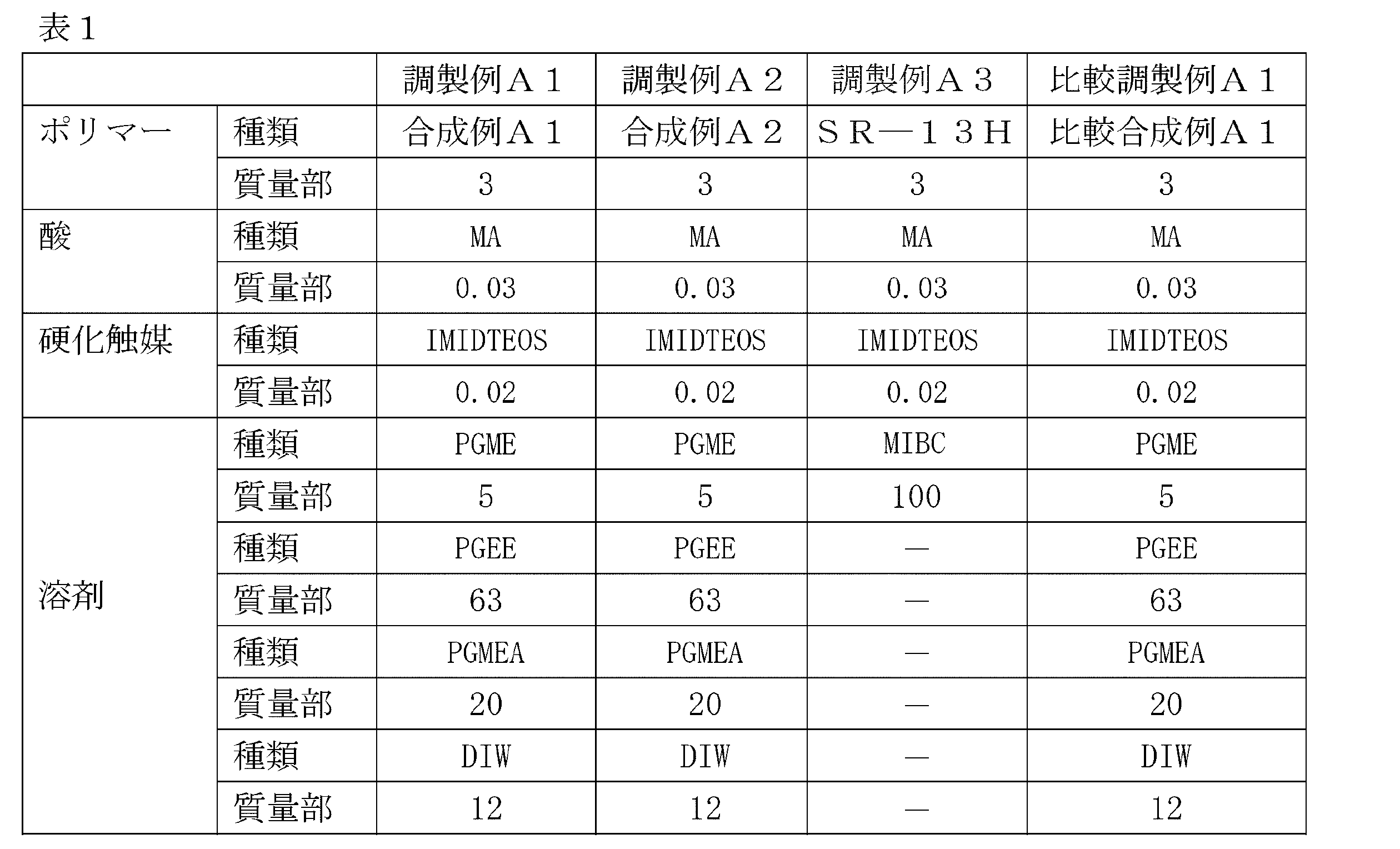
〔塗布液の平坦化性(Si基板上での平坦化性評価)〕
実施例A1、A2、A3および比較例A1における各被覆用ポリシロキサン組成物について、下記のように平坦化性評価を行った。その評価結果を表2に示す。
溝の深さ220nm、幅800nmの段差基板上に、スピンコーターを用いて、回転数1500rpm、60秒間の条件にて、実施例A1、A2、A3、比較例A1の各被覆用ポリシロキサン組成物を塗布し、その後110℃のホットプレート上で1分間乾燥することにより、ポリシロキサン被覆膜を形成した。ポリシロキサン被覆膜の膜厚は90nmとした。次いで、得られたポリシロキサン被覆膜について、断面SEMにより断面の形状を観察し平坦化性を評価した。深さ220nm、幅800nmの溝パターンを観察し、溝底部を基準として膜厚(すなわち、シリコン基板の膜と接する側の界面からポリシロキサン被覆膜の大気と接する側の界面までの長さ)の最も小さい箇所と最も大きい箇所の膜厚を測定し、膜厚差を算出し、膜厚差が少ないものほど平坦化性が良好と評価した。また評価に使用したSEM写真を図1~4に記載する。

2:有機下層膜
3:レジスト組成物
4:第一ポリシロキサン被覆膜
5:第二ポリシロキサン被覆膜
a:密のスペース部の中心でのポリシロキサン被覆膜の凹み深さ
b:オープンスペース部の中心でのポリシロキサン被覆膜の凹み深さ
c:使用した段差基板における当初のスペースの深さ
d:ポリシロキサン被覆膜
e:段差基板
Claims (12)
- 加水分解性シラン原料の加水分解縮合物を含むポリシロキサンと溶媒とを含む、有機パターン上に塗布される有機パターン平坦化用組成物であって、
上記ポリシロキサンが、Si原子に対し、シラノール基を20モル%以下の割合で含むものであり、
上記ポリシロキサンの重量平均分子量が1,000~50,000である、該組成物。 - 上記ポリシロキサンが、式(1):

(式(1)中、R1はアルキル基、アリール基、ハロゲン化アルキル基、ハロゲン化アリール基、アルコキシアリール基、アルケニル基、又はエポキシ基、アクリロイル基、メタクリロイル基、メルカプト基、もしくはシアノ基を有する有機基で且つSi-C結合によりケイ素原子と結合しているものであり、R2はアルコキシ基、アシルオキシ基、又はハロゲン基を示し、aは1を示す。)で示される加水分解性シランを含む加水分解性シラン原料の加水分解縮合物を含む、請求項1に記載の組成物。 - 上記ポリシロキサンが、上記式(1)で示され、aが1である加水分解性シランを100~50モル%、及び上記式(1)で示され、aが2である加水分解性シランを0~50モル%となる割合で含む加水分解性シラン原料の加水分解縮合物を含む、請求項2に記載の組成物。
- 上記ポリシロキサンが、上記式(1)のaが0の加水分解性シランを0~100モル%、及びaが1である加水分解性シランを0~100モル%となる割合で含む加水分解性シラン原料の加水分解縮合物のアルコール及び酸による脱水処理生成物である、請求項2又は3に記載の組成物。
- 上記ポリシロキサンが、上記式(1)のaが1又は2の加水分解性シラン原料の加水分解縮合物の非アルコールと弱酸又は塩基とによる処理生成物である、請求項2又は3のいずれか1項に記載の組成物。
- 弱酸が4~5の酸解離定数を有する酸である、請求項5に記載の組成物。
- 上記有機パターンがレジストパターン、ナノインプリントパターン及び有機下層膜パターンの中から選ばれる、請求項1~6のいずれか1項に記載の組成物。
- 基板上に有機パターンを形成する工程(1)、有機パターンに請求項1~7のいずれか1項に記載の組成物を塗布する工程(3)、有機パターンをエッチング除去してパターンを反転させる工程(4)、を含む半導体装置の製造方法。
- 基板上にレジストを形成する工程(1a)、レジストを露光と現像する工程(2)、現像中又は現像後のレジストパターンに請求項1~7のいずれか1項に記載の組成物を塗布する工程(3a)、レジストパターンをエッチング除去してパターンを反転させる工程(4a)、を含む半導体装置の製造方法。
- 工程(3)の後に、塗膜表面をエッチバックして有機パターン表面を露出する工程(3-1)を含む、請求項8に記載の製造方法。
- 有機パターンに塗布される段差基板平坦化用組成物に含まれるポリシロキサンの製造方法であって、
式(1):

(式(1)中、R1はアルキル基、アリール基、ハロゲン化アルキル基、ハロゲン化アリール基、アルコキシアリール基、アルケニル基、又はエポキシ基、アクリロイル基、メタクリロイル基、メルカプト基、もしくはシアノ基を有する有機基で且つSi-C結合によりケイ素原子と結合しているものであり、R2はアルコキシ基、アシルオキシ基、又はハロゲン基を示し、aは0を示す。)で示され、aが0の加水分解性シランを0~100モル%、及び式(1)で示され、aが1である加水分解性シランを0~100モル%となる割合で含む加水分解性シラン原料の加水分解縮合物を、アルコールと酸で脱水処理する工程を含む、製造方法。 - 有機パターンに塗布される段差基板平坦化用組成物に含まれるポリシロキサンの製造方法であって、
式(1):

(式(1)中、R1はアルキル基、アリール基、ハロゲン化アルキル基、ハロゲン化アリール基、アルコキシアリール基、アルケニル基、又はエポキシ基、アクリロイル基、メタクリロイル基、メルカプト基、もしくはシアノ基を有する有機基で且つSi-C結合によりケイ素原子と結合しているものであり、R2はアルコキシ基、アシルオキシ基、又はハロゲン基を示し、aは1又は2を示す。)で示され、aが1又は2の加水分解性シラン原料の加水分解縮合物を、非アルコールと弱酸又は塩基とで処理する工程を含む、製造方法。
Priority Applications (4)
| Application Number | Priority Date | Filing Date | Title |
|---|---|---|---|
| JP2018501579A JP7143763B2 (ja) | 2016-02-24 | 2017-02-10 | シリコン含有パターン反転用被覆剤 |
| US16/082,241 US11609499B2 (en) | 2016-02-24 | 2017-02-10 | Silicon-containing coating agent for pattern reversal |
| CN201780012899.0A CN108699389B (zh) | 2016-02-24 | 2017-02-10 | 含有硅的图案反转用被覆剂 |
| KR1020187024387A KR102505090B1 (ko) | 2016-02-24 | 2017-02-10 | 실리콘 함유 패턴반전용 피복제 |
Applications Claiming Priority (2)
| Application Number | Priority Date | Filing Date | Title |
|---|---|---|---|
| JP2016033394 | 2016-02-24 | ||
| JP2016-033394 | 2016-02-24 |
Publications (1)
| Publication Number | Publication Date |
|---|---|
| WO2017145809A1 true WO2017145809A1 (ja) | 2017-08-31 |
Family
ID=59685159
Family Applications (1)
| Application Number | Title | Priority Date | Filing Date |
|---|---|---|---|
| PCT/JP2017/004921 Ceased WO2017145809A1 (ja) | 2016-02-24 | 2017-02-10 | シリコン含有パターン反転用被覆剤 |
Country Status (6)
| Country | Link |
|---|---|
| US (1) | US11609499B2 (ja) |
| JP (1) | JP7143763B2 (ja) |
| KR (1) | KR102505090B1 (ja) |
| CN (1) | CN108699389B (ja) |
| TW (1) | TWI731034B (ja) |
| WO (1) | WO2017145809A1 (ja) |
Cited By (3)
| Publication number | Priority date | Publication date | Assignee | Title |
|---|---|---|---|---|
| JPWO2017043344A1 (ja) * | 2015-09-09 | 2018-07-19 | 日産化学工業株式会社 | シリコン含有平坦化性パターン反転用被覆剤 |
| WO2020138189A1 (ja) * | 2018-12-27 | 2020-07-02 | 日産化学株式会社 | 膜形成用組成物 |
| WO2022050405A1 (ja) | 2020-09-07 | 2022-03-10 | 日産化学株式会社 | ウェハー処理方法 |
Citations (9)
| Publication number | Priority date | Publication date | Assignee | Title |
|---|---|---|---|---|
| JP2004359953A (ja) * | 2003-06-02 | 2004-12-24 | Samsung Electronics Co Ltd | シロキサン系樹脂及びこれを用いた半導体層間絶縁膜 |
| JP2005221534A (ja) * | 2004-02-03 | 2005-08-18 | Shin Etsu Chem Co Ltd | 珪素含有レジスト下層膜材料及びパターン形成方法 |
| JP2005336421A (ja) * | 2004-05-31 | 2005-12-08 | Dow Corning Toray Co Ltd | 活性エネルギー線硬化型オルガノポリシロキサン樹脂組成物、光伝送部材およびその製造方法 |
| JP2006307180A (ja) * | 2005-04-01 | 2006-11-09 | Shin Etsu Chem Co Ltd | シルセスキオキサン系化合物混合物、その製造方法及びそれを用いたレジスト組成物並びにパターン形成方法 |
| JP2008266119A (ja) * | 2006-11-24 | 2008-11-06 | Jsr Corp | シリコーン樹脂、シリコーン樹脂組成物およびトレンチアイソレーションの形成方法 |
| JP2009148670A (ja) * | 2007-12-19 | 2009-07-09 | Fujifilm Corp | 塗膜の製造方法および塗膜 |
| WO2010010928A1 (ja) * | 2008-07-24 | 2010-01-28 | 日産化学工業株式会社 | コーティング組成物及びパターン形成方法 |
| JP2011118373A (ja) * | 2009-10-30 | 2011-06-16 | Jsr Corp | 反転パターン形成方法及びポリシロキサン樹脂組成物 |
| JP2015038221A (ja) * | 2007-02-27 | 2015-02-26 | エイゼット・エレクトロニック・マテリアルズ・ユーエスエイ・コーポレイション | ケイ素に基づく反射防止膜用組成物 |
Family Cites Families (24)
| Publication number | Priority date | Publication date | Assignee | Title |
|---|---|---|---|---|
| JP5195428B2 (ja) * | 2006-08-29 | 2013-05-08 | Jsr株式会社 | ネガ型感光性絶縁樹脂組成物及びその硬化物並びにそれを備える回路基板 |
| KR20090057397A (ko) | 2006-09-21 | 2009-06-05 | 제이에스알 가부시끼가이샤 | 실리콘 수지 조성물 및 트렌치 아이솔레이션의 형성 방법 |
| JP5093116B2 (ja) * | 2006-12-21 | 2012-12-05 | Jsr株式会社 | 絶縁膜形成用感光性樹脂組成物及びその硬化膜並びにそれを備える電子部品 |
| KR20090114476A (ko) * | 2007-02-26 | 2009-11-03 | 에이제트 일렉트로닉 머트리얼즈 유에스에이 코프. | 실록산 중합체의 제조 방법 |
| JP5127277B2 (ja) * | 2007-04-05 | 2013-01-23 | 新日鉄住金マテリアルズ株式会社 | 表面平坦性絶縁膜形成用塗布溶液、表面平坦性絶縁膜被覆基材、及び表面平坦性絶縁膜被覆基材の製造方法 |
| US20100178620A1 (en) | 2007-05-21 | 2010-07-15 | Jsr Corporation | Inverted pattern forming method and resin composition |
| EP2113587B9 (de) | 2008-04-28 | 2011-09-07 | ATOTECH Deutschland GmbH | Wässriges saures Bad und Verfahren zum elektrolytischen Abschneiden von Kupfer |
| JP5035151B2 (ja) * | 2008-07-10 | 2012-09-26 | Jsr株式会社 | パターン反転用樹脂組成物及び反転パターン形成方法 |
| JP5438958B2 (ja) | 2008-12-24 | 2014-03-12 | 東京応化工業株式会社 | パターン形成方法および反転パターン形成用材料 |
| JP5413185B2 (ja) * | 2008-12-25 | 2014-02-12 | Jsr株式会社 | ネガ型感放射線性組成物、硬化パターン形成方法および硬化パターン |
| TW201030469A (en) * | 2008-12-25 | 2010-08-16 | Jsr Corp | Negative-tone radiation-sensitive composition, cured pattern forming method, and cured pattern |
| KR101762348B1 (ko) * | 2010-06-11 | 2017-07-27 | 가부시키가이샤 아데카 | 규소 함유 경화성 조성물, 그 규소 함유 경화성 조성물의 경화물 및 그 규소 함유 경화성 조성물로 형성되는 리드 프레임 기판 |
| JP2013540169A (ja) * | 2010-09-22 | 2013-10-31 | ダウ コーニング コーポレーション | 樹脂−直鎖状オルガノシロキサンブロックコポリマーの調製方法 |
| JP5785121B2 (ja) * | 2011-04-28 | 2015-09-24 | 信越化学工業株式会社 | パターン形成方法 |
| TWI618985B (zh) * | 2011-08-10 | 2018-03-21 | 日產化學工業股份有限公司 | 具有碸構造之含矽阻劑底層膜形成組成物 |
| EP2791263B1 (en) * | 2011-12-14 | 2016-08-31 | Dow Corning Corporation | Curable compositions of resin-linear organosiloxane block copolymers |
| KR102086317B1 (ko) * | 2012-03-21 | 2020-03-09 | 다우 실리콘즈 코포레이션 | 수지-선형 오가노실록산 블록 공중합체의 조성물 |
| KR102307208B1 (ko) * | 2012-10-31 | 2021-10-01 | 닛산 가가쿠 가부시키가이샤 | 에스테르기를 갖는 실리콘함유 레지스트 하층막 형성조성물 |
| JP6002554B2 (ja) * | 2012-11-26 | 2016-10-05 | 富士フイルム株式会社 | パターン形成方法、及び、これを用いる電子デバイスの製造方法 |
| US9290623B2 (en) * | 2012-12-19 | 2016-03-22 | Nissan Chemical Industries, Ltd. | Composition for forming silicon-containing resist underlayer film having cyclic diester group |
| WO2014097096A1 (en) * | 2012-12-21 | 2014-06-26 | Koninklijke Philips N.V. | Composition, imprinting ink and imprinting method |
| JP6587065B2 (ja) * | 2014-02-26 | 2019-10-09 | 日産化学株式会社 | レジストパターンに塗布されるポリマー含有塗布液 |
| KR101615544B1 (ko) * | 2014-04-01 | 2016-04-26 | 한국과학기술원 | 가수분해-축합반응을 이용한 투명 실록산 경화물의 제조방법 |
| TWI707400B (zh) * | 2016-02-24 | 2020-10-11 | 日商日產化學工業股份有限公司 | 使用含矽組成物之半導體基板之平坦化方法 |
-
2017
- 2017-02-10 WO PCT/JP2017/004921 patent/WO2017145809A1/ja not_active Ceased
- 2017-02-10 KR KR1020187024387A patent/KR102505090B1/ko active Active
- 2017-02-10 US US16/082,241 patent/US11609499B2/en active Active
- 2017-02-10 JP JP2018501579A patent/JP7143763B2/ja active Active
- 2017-02-10 TW TW106104492A patent/TWI731034B/zh active
- 2017-02-10 CN CN201780012899.0A patent/CN108699389B/zh active Active
Patent Citations (9)
| Publication number | Priority date | Publication date | Assignee | Title |
|---|---|---|---|---|
| JP2004359953A (ja) * | 2003-06-02 | 2004-12-24 | Samsung Electronics Co Ltd | シロキサン系樹脂及びこれを用いた半導体層間絶縁膜 |
| JP2005221534A (ja) * | 2004-02-03 | 2005-08-18 | Shin Etsu Chem Co Ltd | 珪素含有レジスト下層膜材料及びパターン形成方法 |
| JP2005336421A (ja) * | 2004-05-31 | 2005-12-08 | Dow Corning Toray Co Ltd | 活性エネルギー線硬化型オルガノポリシロキサン樹脂組成物、光伝送部材およびその製造方法 |
| JP2006307180A (ja) * | 2005-04-01 | 2006-11-09 | Shin Etsu Chem Co Ltd | シルセスキオキサン系化合物混合物、その製造方法及びそれを用いたレジスト組成物並びにパターン形成方法 |
| JP2008266119A (ja) * | 2006-11-24 | 2008-11-06 | Jsr Corp | シリコーン樹脂、シリコーン樹脂組成物およびトレンチアイソレーションの形成方法 |
| JP2015038221A (ja) * | 2007-02-27 | 2015-02-26 | エイゼット・エレクトロニック・マテリアルズ・ユーエスエイ・コーポレイション | ケイ素に基づく反射防止膜用組成物 |
| JP2009148670A (ja) * | 2007-12-19 | 2009-07-09 | Fujifilm Corp | 塗膜の製造方法および塗膜 |
| WO2010010928A1 (ja) * | 2008-07-24 | 2010-01-28 | 日産化学工業株式会社 | コーティング組成物及びパターン形成方法 |
| JP2011118373A (ja) * | 2009-10-30 | 2011-06-16 | Jsr Corp | 反転パターン形成方法及びポリシロキサン樹脂組成物 |
Cited By (6)
| Publication number | Priority date | Publication date | Assignee | Title |
|---|---|---|---|---|
| JPWO2017043344A1 (ja) * | 2015-09-09 | 2018-07-19 | 日産化学工業株式会社 | シリコン含有平坦化性パターン反転用被覆剤 |
| WO2020138189A1 (ja) * | 2018-12-27 | 2020-07-02 | 日産化学株式会社 | 膜形成用組成物 |
| JPWO2020138189A1 (ja) * | 2018-12-27 | 2021-11-18 | 日産化学株式会社 | 膜形成用組成物 |
| JP7513959B2 (ja) | 2018-12-27 | 2024-07-10 | 日産化学株式会社 | 膜形成用組成物 |
| TWI875729B (zh) * | 2018-12-27 | 2025-03-11 | 日商日產化學股份有限公司 | 膜形成用組成物 |
| WO2022050405A1 (ja) | 2020-09-07 | 2022-03-10 | 日産化学株式会社 | ウェハー処理方法 |
Also Published As
| Publication number | Publication date |
|---|---|
| CN108699389A (zh) | 2018-10-23 |
| TW201804255A (zh) | 2018-02-01 |
| JP7143763B2 (ja) | 2022-09-29 |
| CN108699389B (zh) | 2020-10-27 |
| KR102505090B1 (ko) | 2023-03-02 |
| KR20180116287A (ko) | 2018-10-24 |
| US11609499B2 (en) | 2023-03-21 |
| TWI731034B (zh) | 2021-06-21 |
| US20190339618A1 (en) | 2019-11-07 |
| JPWO2017145809A1 (ja) | 2018-12-13 |
Similar Documents
| Publication | Publication Date | Title |
|---|---|---|
| KR102426414B1 (ko) | Soc 패턴 상에서의 패턴반전을 위한 피복용 조성물 | |
| KR102830156B1 (ko) | 실리콘 함유 조성물을 이용한 반도체 기판의 평탄화방법 | |
| US12084592B2 (en) | Coating composition for pattern inversion | |
| JP7157392B2 (ja) | アルカリ性現像液可溶性シリコン含有レジスト下層膜形成組成物 | |
| WO2020138092A1 (ja) | 水素ガスを用いた前処理によるレジスト下層膜のエッチング耐性を向上する方法 | |
| JP6738049B2 (ja) | シリコン含有平坦化性パターン反転用被覆剤 | |
| JP7143763B2 (ja) | シリコン含有パターン反転用被覆剤 | |
| WO2017043635A1 (ja) | ビニル基又は(メタ)アクリロキシ基含有ポリシロキサンを含むレジストパターン塗布用組成物 | |
| JP2020027841A (ja) | 光または電子線に応答するパターン反転組成物およびそれを用いたパターン形成方法 |
Legal Events
| Date | Code | Title | Description |
|---|---|---|---|
| ENP | Entry into the national phase |
Ref document number: 2018501579 Country of ref document: JP Kind code of ref document: A |
|
| ENP | Entry into the national phase |
Ref document number: 20187024387 Country of ref document: KR Kind code of ref document: A |
|
| NENP | Non-entry into the national phase |
Ref country code: DE |
|
| 121 | Ep: the epo has been informed by wipo that ep was designated in this application |
Ref document number: 17756250 Country of ref document: EP Kind code of ref document: A1 |
|
| 122 | Ep: pct application non-entry in european phase |
Ref document number: 17756250 Country of ref document: EP Kind code of ref document: A1 |