WO2017145910A1 - Filtre à densité neutre (nd) à matériau de base en plastique, et filtre nd à matériau de base en plastique pour lunettes - Google Patents
Filtre à densité neutre (nd) à matériau de base en plastique, et filtre nd à matériau de base en plastique pour lunettes Download PDFInfo
- Publication number
- WO2017145910A1 WO2017145910A1 PCT/JP2017/005732 JP2017005732W WO2017145910A1 WO 2017145910 A1 WO2017145910 A1 WO 2017145910A1 JP 2017005732 W JP2017005732 W JP 2017005732W WO 2017145910 A1 WO2017145910 A1 WO 2017145910A1
- Authority
- WO
- WIPO (PCT)
- Prior art keywords
- layer
- film
- nio
- substrate
- base material
- Prior art date
- Legal status (The legal status is an assumption and is not a legal conclusion. Google has not performed a legal analysis and makes no representation as to the accuracy of the status listed.)
- Ceased
Links
Images


Classifications
-
- G—PHYSICS
- G02—OPTICS
- G02B—OPTICAL ELEMENTS, SYSTEMS OR APPARATUS
- G02B5/00—Optical elements other than lenses
- G02B5/20—Filters
- G02B5/205—Neutral density filters
-
- B—PERFORMING OPERATIONS; TRANSPORTING
- B32—LAYERED PRODUCTS
- B32B—LAYERED PRODUCTS, i.e. PRODUCTS BUILT-UP OF STRATA OF FLAT OR NON-FLAT, e.g. CELLULAR OR HONEYCOMB, FORM
- B32B27/00—Layered products comprising a layer of synthetic resin
- B32B27/06—Layered products comprising a layer of synthetic resin as the main or only constituent of a layer, which is next to another layer of the same or of a different material
- B32B27/08—Layered products comprising a layer of synthetic resin as the main or only constituent of a layer, which is next to another layer of the same or of a different material of synthetic resin
-
- B—PERFORMING OPERATIONS; TRANSPORTING
- B32—LAYERED PRODUCTS
- B32B—LAYERED PRODUCTS, i.e. PRODUCTS BUILT-UP OF STRATA OF FLAT OR NON-FLAT, e.g. CELLULAR OR HONEYCOMB, FORM
- B32B27/00—Layered products comprising a layer of synthetic resin
- B32B27/28—Layered products comprising a layer of synthetic resin comprising synthetic resins not wholly covered by any one of the sub-groups B32B27/30 - B32B27/42
-
- B—PERFORMING OPERATIONS; TRANSPORTING
- B32—LAYERED PRODUCTS
- B32B—LAYERED PRODUCTS, i.e. PRODUCTS BUILT-UP OF STRATA OF FLAT OR NON-FLAT, e.g. CELLULAR OR HONEYCOMB, FORM
- B32B27/00—Layered products comprising a layer of synthetic resin
- B32B27/40—Layered products comprising a layer of synthetic resin comprising polyurethanes
-
- B—PERFORMING OPERATIONS; TRANSPORTING
- B32—LAYERED PRODUCTS
- B32B—LAYERED PRODUCTS, i.e. PRODUCTS BUILT-UP OF STRATA OF FLAT OR NON-FLAT, e.g. CELLULAR OR HONEYCOMB, FORM
- B32B7/00—Layered products characterised by the relation between layers; Layered products characterised by the relative orientation of features between layers, or by the relative values of a measurable parameter between layers, i.e. products comprising layers having different physical, chemical or physicochemical properties; Layered products characterised by the interconnection of layers
- B32B7/02—Physical, chemical or physicochemical properties
- B32B7/023—Optical properties
-
- B—PERFORMING OPERATIONS; TRANSPORTING
- B32—LAYERED PRODUCTS
- B32B—LAYERED PRODUCTS, i.e. PRODUCTS BUILT-UP OF STRATA OF FLAT OR NON-FLAT, e.g. CELLULAR OR HONEYCOMB, FORM
- B32B9/00—Layered products comprising a layer of a particular substance not covered by groups B32B11/00 - B32B29/00
-
- G—PHYSICS
- G02—OPTICS
- G02B—OPTICAL ELEMENTS, SYSTEMS OR APPARATUS
- G02B1/00—Optical elements characterised by the material of which they are made; Optical coatings for optical elements
- G02B1/10—Optical coatings produced by application to, or surface treatment of, optical elements
- G02B1/11—Anti-reflection coatings
- G02B1/113—Anti-reflection coatings using inorganic layer materials only
- G02B1/115—Multilayers
-
- G—PHYSICS
- G02—OPTICS
- G02B—OPTICAL ELEMENTS, SYSTEMS OR APPARATUS
- G02B1/00—Optical elements characterised by the material of which they are made; Optical coatings for optical elements
- G02B1/10—Optical coatings produced by application to, or surface treatment of, optical elements
- G02B1/14—Protective coatings, e.g. hard coatings
-
- G—PHYSICS
- G02—OPTICS
- G02B—OPTICAL ELEMENTS, SYSTEMS OR APPARATUS
- G02B5/00—Optical elements other than lenses
-
- G—PHYSICS
- G02—OPTICS
- G02C—SPECTACLES; SUNGLASSES OR GOGGLES INSOFAR AS THEY HAVE THE SAME FEATURES AS SPECTACLES; CONTACT LENSES
- G02C7/00—Optical parts
- G02C7/10—Filters, e.g. for facilitating adaptation of the eyes to the dark; Sunglasses
-
- G—PHYSICS
- G02—OPTICS
- G02C—SPECTACLES; SUNGLASSES OR GOGGLES INSOFAR AS THEY HAVE THE SAME FEATURES AS SPECTACLES; CONTACT LENSES
- G02C7/00—Optical parts
- G02C7/10—Filters, e.g. for facilitating adaptation of the eyes to the dark; Sunglasses
- G02C7/107—Interference colour filters
-
- B—PERFORMING OPERATIONS; TRANSPORTING
- B32—LAYERED PRODUCTS
- B32B—LAYERED PRODUCTS, i.e. PRODUCTS BUILT-UP OF STRATA OF FLAT OR NON-FLAT, e.g. CELLULAR OR HONEYCOMB, FORM
- B32B2255/00—Coating on the layer surface
- B32B2255/10—Coating on the layer surface on synthetic resin layer or on natural or synthetic rubber layer
-
- B—PERFORMING OPERATIONS; TRANSPORTING
- B32—LAYERED PRODUCTS
- B32B—LAYERED PRODUCTS, i.e. PRODUCTS BUILT-UP OF STRATA OF FLAT OR NON-FLAT, e.g. CELLULAR OR HONEYCOMB, FORM
- B32B2255/00—Coating on the layer surface
- B32B2255/20—Inorganic coating
-
- B—PERFORMING OPERATIONS; TRANSPORTING
- B32—LAYERED PRODUCTS
- B32B—LAYERED PRODUCTS, i.e. PRODUCTS BUILT-UP OF STRATA OF FLAT OR NON-FLAT, e.g. CELLULAR OR HONEYCOMB, FORM
- B32B2551/00—Optical elements
Definitions
- the present invention relates to an ND (Neutral Density) filter whose base material is made of plastic, and an ND filter for glasses using the ND filter.
- ND Neutral Density
- This ND filter is formed by laminating a plurality of light absorption films and a plurality of dielectric films on one surface or both surfaces of a transparent substrate, and the light absorption film is composed of single germanium or single silicon. And a mixture of nickel and its oxide (Ni + NiO x ).
- the thing made from a plastic is preferable from a viewpoint of lightness, the difficulty of a crack, and dyeing
- the substrate is made of plastic, it is necessary to consider that the plastic is easy to absorb water and that the absorbed water is easily released. That is, the moisture released from the substrate gradually acts on the light absorption film and the dielectric film on the substrate, and the adhesion of these films gradually decreases, which can be a factor of gradually degrading the weather resistance and the like.
- Patent Document 1 there is no particular description about moisture from a plastic substrate, and in Patent Document 1 (plastic substrate), there is room for further improvement in terms of lifetime such as weather resistance.
- the present invention has the object of providing an ND filter and an ND filter for spectacles that have a base material (substrate) made of plastic and excellent in durability.
- an invention according to claim 1 is an ND filter comprising: a base material made of plastic; and a light absorption film having a plurality of layers disposed on at least one surface of the base material.
- the first layer of the layer from the substrate side of the light absorption layer is the Al 2 O 3 layer consisting of SiO 2 layer or Al 2 O 3 of SiO 2
- the light-absorbing film, NiO x (x is 0 or more and 1 or less) includes from consisting NiO x layer and CoO x '(x' is 0 to 1.5) comprising CoO x 'at least one of one or more of the layers from , At least one of at least one of the NiO x layer and the CoO x ′ layer is adjacent to the substrate side adjacent layer that is the layer adjacent on the substrate side, and adjacent to the opposite side.
- the invention according to claim 2 is the above invention, wherein at least one of the NiO x layer and the CoO x ′ layer has a physical film thickness of 6 nanometers or less. It is a feature.
- the invention according to claim 3 is characterized in that, in the above invention, the substrate side adjacent layer or the opposite side adjacent layer is a silica compound layer made of a silica compound.
- the invention according to claim 4 is characterized in that, in the above invention, the SiO 2 layer or the Al 2 O 3 layer has a density to the extent that it is formed by vapor deposition without ion assist.
- the invention according to claim 5 is characterized in that, in the above-mentioned invention, the light absorption film is formed by alternately arranging low refractive index layers and high refractive index layers.
- the invention according to claim 6 is characterized in that, in the above invention, the base material has a front surface and a back surface, and the light absorption film is disposed on the back surface.
- the invention according to claim 7 is the above invention, wherein an antireflection film is disposed on the surface.
- the invention according to claim 8 is a plastic substrate ND filter for eyeglasses, characterized by including the plastic substrate ND filter of the invention.
- an ND filter and an ND filter for spectacles that are made of plastic and have excellent durability.
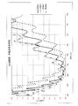
- 4 is a graph showing spectral transmittance distributions in the visible range of Examples 1 to 4 according to the present invention.
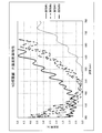
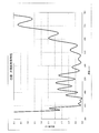
- 7 is a graph showing spectral transmittance distributions in the visible range of Examples 5 to 8 according to the present invention. It is a graph by which the spectral transmittance distribution of a commercially available dyed spectacle lens is shown.
- 6 is a graph showing spectral reflectance distribution (single side) in the visible range on the concave surface (ND film formation surface) side of Examples 1 to 4.
- 10 is a graph showing spectral reflectance distribution (single side) in the visible range on the concave surface (ND film-forming surface) side of Examples 5 to 8.
- 10 is a graph showing spectral reflectance distributions (single side, common) in the visible range relating to the convex surface side of Examples 1 to 9.
- the ND filter according to the present invention has a light whose wavelength is at least in the visible range (for example, 400 nm to 800 nm, 400 nm to 760 nm, 400 nm to 700 nm, 410 nm to 760 nm, or 420 nm to 760 nm). It is a filter that uniformly absorbs (visible light).
- the substrate of the ND filter is made of transparent (including translucent as appropriate) plastic.
- the material of the substrate include polyurethane resin, thiourethane resin, episulfide resin, polycarbonate resin, acrylic resin, polyether sulfone resin, poly-4-methylpentene-1 resin, and diethylene glycol bisallyl carbonate resin.
- the base material may be a convex lens, a concave lens, a flat lens, or any power and progression.
- the ND filter of the present invention may be used for any application as long as the base material is made of plastic, and is preferably a part of a camera lens system (for protecting other lenses or for incorporating a camera body). And for projectors, binoculars, and telescopes, and more preferably for spectacles (use for spectacle lenses themselves or lenses that cover spectacle lenses).
- the optical multilayer film is formed on one side or both sides of the substrate.
- the optical multilayer film mainly has a function of uniformly absorbing visible light, and further has a function of appropriately preventing visible light reflection.
- the optical multilayer film for the purpose of absorbing visible light or a portion thereof is a light absorbing film, and when the light absorbing film is a single layer, it may be a light absorbing layer.
- the optical multilayer film or its part for the purpose of preventing reflection of visible light is an antireflection film.
- the antireflection film may include a light absorption film.
- the optical multilayer film may be composed only of the light absorption film, or may be one in which an antifouling film or a protective film is added to the surface side (air side) of the light absorption film,
- One or a plurality of intermediate layers including a hard coat film may be added to the base material side, or a single layer for other purposes such as improving conductivity in or outside the light absorption film.
- a plurality of layers or films may be added, or a combination thereof may be used.
- the hard coat film, the conductive layer, the antireflection film, and the like may not be included in the optical multilayer film, or may be separate optical multilayer films in combination with each other or in combination thereof.
- the hard coat film is formed from, for example, an organosiloxane compound, or formed from an organosilicon compound or an acrylic compound.
- a primer layer may be provided as a lower layer (layer on the substrate side) of the hard coat film.
- the primer layer is formed of at least one of polyurethane resin, acrylic resin, methacrylic resin, and organosilicon resin, for example.
- the antireflection film is formed of, for example, a plurality of types of dielectric materials including a low refractive index material and a high refractive index material.
- the low refractive index material at least one of the exemplary silicon oxide (especially SiO 2) or magnesium fluoride (in particular MgF 2), as the high refractive index material, zirconium oxide (in particular ZrO 2), titanium oxide (especially TiO 2 ), at least one of tantalum oxide (particularly Ta 2 O 5 ) and niobium oxide (particularly Nb 2 O 5 ).
- the antireflection film is preferably formed by alternately laminating a low refractive index material and a high refractive index material with one of them as the base material side.
- the light absorption film is formed to include one or more light absorption layers made of at least one of nickel (Ni) and cobalt (Co).
- Ni may be a simple substance, but is preferably an unsaturated metal oxide film (NiO x ; x is more than 0 and 1 or less).
- the value of x can be adjusted by, for example, Ni being used as a vapor deposition material and vapor deposition in a state where oxygen gas is supplied at a predetermined flow rate in a vapor deposition vacuum device.
- Co may be a simple substance, but is preferably an unsaturated metal oxide film (CoO x ′ ; x ′ exceeds 0 and is 1.5 or less).
- the light absorption film may be formed as a multilayer film having other layers. Examples of other layers in this case include an SiO 2 layer, a ZrO 2 layer, an aluminum oxide (particularly Al 2 O 3 ) layer, a silica compound layer, or a combination thereof.
- the silica compound is a compound of silicon or a mixture of the compound and another compound, preferably a mixture of silicon oxide and aluminum oxide, more preferably a mixture of SiO 2 and Al 2 O 3 . It is. At least one light-absorbing layer, i.e. NiO x layer (x is 0 or more and 1 or less) and CoO x 'layer (x' is 0 to 1.5) in at least one of, the base-side adjacent layer,
- the adjacent layers on the opposite side (air side) are layers made of different materials.
- the substrate side adjacent layer is an Al 2 O 3 layer
- the opposite side adjacent layer is a silica compound layer.
- the substrate side adjacent layer and the opposite side adjacent layer in at least one of the NiO x layers may be layers made of different materials.
- the substrate side adjacent layer and the opposite side adjacent layer in at least one of the NiO x layers may be layers made of different materials.
- both the NiO x layer and the CoO x ′ layer are provided one by one, in either one of the NiO x layer and the CoO x ′ layer, the substrate side adjacent layer and the opposite side adjacent layer are different from each other. It is sufficient to be a layer of.
- any one of the NiO x layer or the CoO x ′ layer is opposite to the substrate side adjacent layer.
- the adjacent layers may be layers made of different materials. If the base layer side adjacent layer or the opposite side adjacent layer is a silica compound layer, the silica compound layer has a density that does not allow moisture to pass as much as the ZrO 2 layer, and is not so dense that it completely seals moisture. It is preferable because the moisture permeability is just right.
- the first layer (initial layer) from the substrate side of the light absorption film is an SiO 2 layer or an Al 2 O 3 layer.
- the initial layer of the light absorption film has a density that can be formed by vapor deposition without ion assist. It is extremely difficult for those skilled in the art to directly measure the density of the deposited film including the initial layer. Also, it is easy to understand for those skilled in the art to specify the degree of density of the deposited film by the presence or absence of ion assist during deposition.
- the light absorption film may have a function as an antireflection film in addition to the light absorption function by alternately arranging the low refractive index layer and the high refractive index layer.
- the NiO x layer and the CoO x ′ layer may be treated as a high refractive index layer.
- the substrate preferably has a front and back surface such as for glasses.
- the front side of the ND filter substrate for glasses is the environment side, and the back side is the face side.
- the optical multilayer film preferably has an antireflection film disposed on the front side of the substrate and a light absorption film disposed on the back side.
- the anti-reflection coating is more durable than the light-absorbing film, the anti-reflection coating is relatively durable on the front side exposed to harsh environments, and the light-absorbing film is relatively protected on the back side. By disposing, it is possible to improve the overall durability while ensuring the light absorption (ND) and antireflection functions and realizing good characteristics.
- ND filter is preferably used for glasses.
- the ND filter itself may be a spectacle lens, or the ND filter may be prepared so as to cover another spectacle lens.
- General eyeglasses (sunglasses) have a visible light absorptance that varies greatly from wavelength to wavelength in the visible range, and look different from the naked eye in color, contrast, etc.
- the ND filter for eyeglasses of the present invention thus, visibility equal to that of the naked eye can be provided by uniform absorption of visible light in the visible range.
- Examples 1 to 8, Comparative Examples 1 to 7 several preferred examples of the present invention and comparative examples not belonging to the present invention will be described (Examples 1 to 8, Comparative Examples 1 to 7).
- an Example may turn into a comparative example or a comparative example may turn into an Example by the view of this invention.
- convex lenses for spectacles that are round balls having a diameter of 75 millimeters (mm) were produced.
- the frequency is S-4.00
- the convex side (front side) is aspherical
- the center thickness is 1.2 mm.
- the substrate both are formed of episulfide resin, the refractive index 1.76, Abbe number 30, a specific gravity of 1.49 g / cm 3 (grams per cubic centimeter).
- a hard coat film (HC film) was formed on both the front and back surfaces of the substrate. Each hard coat film was formed by applying the same hard coat liquid in the same manner.
- the hard coat solution was prepared as follows.
- the hard coat solution was uniformly spread on the surface of the substrate by a spin coat method, and then was hardened by heating in an environment of 120 ° C. for 1.5 hours to form a hard coat film.
- the physical film thickness of the hard coat film thus formed was 2.5 ⁇ m (micrometer).
- an antireflection film (AR film) and a water repellent layer were formed on the convex surface (surface) side of the substrate. That is, it is set on a jig (dome) to which a base material with a hard coat film is fixed, and is put into a vacuum apparatus from a door. Thereafter, the door is closed and the inside of the vacuum device is evacuated. In order to remove moisture from the substrate, the temperature in the vacuum apparatus is maintained at 60 ° C. When the degree of vacuum in the vacuum apparatus reaches 1.0E-03 (1.0 ⁇ 10 ⁇ 3 ) Pa (Pascal), the following film formation is started.
- the substrate surface is activated by irradiating the substrate surface with oxygen ions for 60 seconds.
- SiO 2 that is a low refractive material and ZrO 2 that is a high refractive material are alternately deposited for each predetermined time, and each layer has a desired film thickness, so that all five antireflection films are convex surfaces of the substrate.
- a film was formed on top.
- a water repellent was deposited on the convex side of the substrate with the antireflection film in a vacuum apparatus, and a water repellent layer was formed on the antireflection film (outermost layer).
- Table 1 The structures of the optical multilayer films on the convex surface side in Examples 1 to 8 and Comparative Examples 1 to 7 are as shown in Table 1 below. Unless otherwise specified, the film thickness is a physical film thickness.
- the light absorption film and the water repellent layer were formed on the concave surface (back surface) side of the substrate. That is, the light absorption film is formed by adjusting the conditions at the time of starting the film formation, similarly to the formation of the antireflection film. In the film formation, after irradiating oxygen ions in the same manner, the next material was formed under the following conditions.
- the light-absorbing film deposition ions were not irradiated except for the first oxygen ion irradiation, and the light-absorbing film was deposited in a state without ion assist (in a state other than Ion Assist Deposition). As SiO 2, Canon Optron Co., Ltd.
- SiO 2 is used, it was deposited at a deposition rate 10.0 ⁇ / s (Angstrom per second).
- ZrO 2 “ZrO 2 ” manufactured by Canon Optron Co., Ltd. was used, and vapor deposition was performed at a deposition rate of 6.0 ⁇ / s.
- the weight of SiO 2 is higher than the weight of Al 2 O 3.
- the weight ratio of Al 2 O 3 to the weight ratio of SiO 2 is about several percent.
- the weight ratio between SiO 2 and Al 2 O 3 is not particularly limited, and the component of the silica compound is not limited to SiO 2 and Al 2 O 3 .
- NiO x and Co for CoO x ′ those manufactured by Kojundo Chemical Laboratory Co., Ltd. were used, and each was deposited at a deposition rate of 3.0 ⁇ / s.
- the oxygen gas is supplied at a flow rate 10sccm (standard cubic centimeter per minute) , NiO x layer and CoO x 'layer is formed.
- a water repellent layer was formed on the light absorbing film (air side) in the same manner as that on the antireflection film. Examples 1 to 8 and Comparative Examples 1 to 7 differ from each other only in the configuration of the light absorption film. Each configuration is as described in Tables 2 to 5 below.
- Table 6 shows the result of the test regarding the presence / absence of ion assist and the density of the vapor deposition film (water vapor permeability closely related thereto) concerning the SiO 2 film and the Al 2 O 3 film.
- the "No.” column in Table 6 describes the order from the one having the highest water vapor permeability.
- This test uses a PET (polyethylene terephthalate) film as a base material, and changes the presence or absence of ion assist in the case of only the base material, and the SiO 2 film, Al 2 O 3 film, and SiO 2 + Al 2 O 3 mixed film on the base material
- the water vapor permeability (gram per cubic meter per day, g / m 2 ⁇ day) in the case of vapor deposition was investigated. In the case of only the base material, the water vapor permeability is 7.29.
- the SiO 2 film, the Al 2 O 3 film, the SiO 2 + Al 2 O 3 mixed film has a film thickness of 90.3 without ion assist.
- the water vapor permeability is 6.75, 6.28, 6.12, which is slightly lower than that of the base material alone.
- SiO 2 film, Al 2 O 3 film, the SiO 2 + Al 2 O 3 mixed film because hinder the permeation of water vapor.
- the SiO 2 film is ion-assisted (deposition with an ion gun acceleration voltage of 900 volts (V), an acceleration current of 900 milliamperes (mA), a bias current of 600 mA, and an introduced oxygen (O 2 ) gas of 50 sccm) with a film thickness of 69.1 nm. In this case, the water vapor permeability is further reduced to 3.77.
- the density of the SiO 2 film formed by ion-assisted deposition is larger than that without ion assist, and the SiO 2 film having such a high density further hinders the transmission of water vapor.
- the Al 2 O 3 film is deposited with an ion assist (acceleration voltage 1000 V, acceleration current 1000 mA, bias current 600 mA, introduced oxygen gas 50 sccm) and a film thickness of 79.0 nm, the water vapor permeability is 0.89. Decrease greatly. This is because the density of the Al 2 O 3 film formed by ion-assisted deposition is larger than the density without ion assist, and such a high-density Al 2 O 3 film further hinders the transmission of water vapor.
- the SiO 2 + Al 2 O 3 mixed film is deposited with a film thickness of 75.0 nm in the same ion assist state as the SiO 2 film, the water vapor permeability becomes as small as 1.61. This is because the density of the SiO 2 + Al 2 O 3 mixed film formed by ion-assisted deposition is larger than that without ion assist, and the higher density of the SiO 2 + Al 2 O 3 mixed film is made of water vapor. This is because transmission is further hindered.
- FIG. 1 is a graph showing the spectral transmittance distribution in the visible range of Examples 1 to 4.
- the spectral transmittance distribution was measured with a spectrophotometer (U-4100 manufactured by Hitachi High-Technologies Corporation).
- the transmittance in the visible region is contained in a band-like region having 51 ⁇ 3%, and the visible light is uniformly absorbed at an absorption rate of about 50%.
- the ND filter for spectacles has a color that is recognized when worn without changing much from the naked eye view. The absorption rate when absorbing uniformly can be changed variously.
- FIG. 2 is a graph showing the spectral transmittance distribution in the visible range of Examples 5 to 8.
- Example 5 (NiO x layer) and Example 6 (CoO x ′ layer) exhibit the same spectral transmittance distribution as in Examples 1 to 4, and each of L, a, and b is the same as in Examples 1 to 4. Has a value.
- Example 5 the transmittance in the visible region is within the band-like region of 54 ⁇ 3%, and the visible light is uniformly absorbed at an absorption rate of about 46%, and the gray appearance is This is an ND filter for eyeglasses in which the color perceived at the time of wearing is not so different from that of naked eyes. Further, comparing Examples 5 and 6, it can be seen that the NiO x layer and the CoO x ′ layer have similar characteristics and can be used in the same manner. In Example 7, the number of light-absorbing layers (NiO x layers) is increased to 3 layers as compared with 2 layers in Examples 1 to 5, and thus the visible light absorption rate is higher than those in Examples 1 to 5. It has become.
- Example 7 the transmittance in the visible region is within a band-like region of 31 ⁇ 2%, and visible light is uniformly absorbed at an absorption rate of about 70%, and is recognized at the time of wearing even though it has a gray appearance.
- This is an ND filter for spectacles whose color is not so different from that of naked eyes.
- the seventh embodiment has the same values of a and b as the first to sixth embodiments, and the L value is smaller than the first to sixth embodiments.
- both the NiO x layer and the CoO x ′ layer are used as the light absorption layer.
- Example 8 the transmittance in the visible region is within a band-like region of 47 ⁇ 2%, and the visible light is uniformly absorbed at an absorption rate of about 53%, and is recognized at the time of wearing even though it has a gray appearance.
- This is an ND filter for spectacles whose color is not so different from that of naked eyes.
- Example 8 has the same values of a and b as in Examples 1 to 6, and the L value is slightly reduced compared to Examples 1 to 6.
- FIG. 3 is a graph showing the spectral transmittance distribution of a dyed spectacle lens commercially available as gray sunglasses (50% concentration).
- This dyed eyeglass lens has a gray color as in Examples 1 to 8, and has a number of extreme values in the range of 45% to 94% in the spectral transmittance distribution in the visible region. The color of is greatly different from the color of the naked eye.
- FIG. 4 is a graph showing the spectral reflectance distribution (single side) in the visible range on the concave surface (ND film formation surface) side of Examples 1 to 4.
- the spectral reflectance distribution was measured by a reflectance measuring device (USPM-RU manufactured by Olympus Corporation).
- USPM-RU manufactured by Olympus Corporation
- the reflectance is generally 5% or less in the visible region, and the minimum value of the reflectance distribution in the green region (450 nm to 580 nm or less) that is greatly involved in the visibility (overall) Therefore, each light absorption film also has a function as an antireflection film.
- FIG. 5 is a graph similar to FIG. 4 on the concave surface (ND film formation surface) side of Examples 5 to 8.
- the reflectance is generally 5% or less in the visible region, and the reflectance distribution in the green region or its adjacent region (about 440 nm to 580 nm or less) that is greatly involved in visibility.
- each light absorption film also has a function as an antireflection film.
- FIG. 6 is a graph showing the spectral reflectance distribution (single side, common) in the visible range on the convex surface side of Examples 1 to 8 measured in the same manner.
- the reflectance is generally 5% or less in the visible region, and the reflectance is 2% or less in the region of 430 nm to 670 nm, which is the majority of the visible region.
- Tables 8 to 11 show the results of various tests relating to durability, that is, constant temperature and humidity test, concave weathering adhesion test, and salt water boiling test, for Examples 1 to 8 and Comparative Examples 1 to 7. Is shown.
- a constant temperature and humidity tester LHU-113 manufactured by ESPEC CORP.
- each ND filter was put in a test machine that was in an environment of 60 ° C. and 95%. After 1 day, 3 days, and 7 days from the start of charging, the ND filter was once taken out, and the presence or absence of appearance abnormalities such as swelling, discoloration, and cracks was observed.
- the ND filter is put into a sunshine weather meter (S80B, manufactured by Suga Test Instruments Co., Ltd.), and is taken out when the feeding time reaches 60 hours (hr), and the above-described cell formation, cellophane tape peeling and massing are performed five times. Number confirmation was done. Similarly, when the charging time became 120, 180, and 240 hours in total after the charging, the above-mentioned grid formation, stripping of the cellophane tape, and confirmation of the number of grids were performed.
- the salt water boiling test 45 g of sodium chloride and 1000 g of pure water were mixed to produce salt water, and the salt water was brought into a boiling state by a heater. And after each ND filter is immersed in boiling salt water and the total immersion time is 10, 20, 30, 40 minutes, the ND filter is taken out and the appearance is observed in the same manner as the constant temperature and humidity test. It was.
- Example 1 to 8 In all of Examples 1 to 8 and Comparative Examples 1 to 7, no abnormality in appearance such as peeling was observed in the salt water boiling test. Further, in Examples 1 to 8, in the constant temperature and humidity test, no abnormal appearance was observed even after 7 days (no change). However, in Example 5, no abnormality in appearance was observed after 3 days, but discoloration of the peripheral portion and generation of cracks were observed after 7 days. In Examples 1 to 8, no peeling was observed in all the squares in the weather resistance adhesion test (100/100).
- Comparative Example 1 in the weather resistance adhesion test, although partial peeling within one square was observed after completion of the total of five peelings in 120 hours and 180 hours (99.5 / 100), other peeling was observed. Good weather resistance was shown. However, in the constant temperature and humidity test, discoloration of the central part was observed after 1 day, and cracks were observed after 3 days. Discoloration is observed in the NiO x layer, and it is considered that the discoloration is due to the action of moisture. The crack is generated on the concave surface, and is considered to be generated according to the stress balance state of the light absorption film. In Comparative Example 1, the first layer from the substrate side (hereinafter the same) is not a SiO 2 layer or an Al 2 O 3 layer but a ZrO 2 layer.
- the ZrO 2 layer has a film density that is too small compared to the SiO 2 layer or Al 2 O 3 layer, allowing water vapor to pass through, and the moisture from the plastic substrate immediately reaches the second and subsequent layers, especially the NiO x layer. It is thought to affect and cause discoloration. From the viewpoint of improving the film density of the first layer, it is assumed that the density is increased by depositing the first layer of Examples 1 to 8 with ion assist. However, with ion assist, the density is too high so that water vapor hardly passes (see Table 6), and the moisture of the base material is accumulated by losing the escape field on the concave surface.
- the light-absorbing film passes through a weak point at a single point, and exhibits a point-like appearance abnormality.
- the first layer has a density related to a state without ion assist.
- the adjacent layer on the substrate side of the two NiO x layers and the adjacent layer on the opposite side are both SiO 2 + Al 2 O 3 mixed layers.
- the SiO 2 + Al 2 O 3 mixed layer has a relatively high density and hardly allows moisture to pass through compared to the SiO 2 layer and the Al 2 O 3 layer (having a high packing effect due to a dense structure).
- Example 1 the second layer of Al 2 O 3 which is the base layer side adjacent layer of the third layer of NiO x is mixed with the fourth layer of SiO 2 + Al 2 O 3 which is the opposite side adjacent layer. Since the material is different from the layer, stress can be released from the adjacent layer on the base material side.
- the base layer side adjacent layer (fourth layer) and the opposite side adjacent layer (sixth layer) of the fifth NiO x layer are both SiO 2 + Al 2 O 3 mixed layers, but the second layer Al 2 Stress can be relieved by the O 3 layer.
- the sixth layer SiO 2 + Al 2 O 3 mixed layer which is the adjacent layer on the opposite side of the fifth NiO x layer, is the fourth layer Al 2 O 3 which is the substrate side adjacent layer. Since the material is different from the layer, stress can be released from the adjacent layer on the opposite side. Further, CoO x 'layer and, NiO x layer and CoO x Example 8' of Example 6 is also in at least one of the layers, as with NiO x layers of Examples 1 to 5 and 7, at least one light-absorbing If the materials of the base layer side adjacent layer and the opposite side adjacent layer are different from each other in the layer, the stress is relieved and the generation of cracks is prevented. It should be noted that the packing effect and the stress difference in SiO 2 + Al 2 O 3 mixed layer, it is same tendency in other silica compounds.
- Comparative Example 2 in the weather resistance adhesion test, no peeling was observed at any time, and good weather resistance was shown. However, in the constant temperature and humidity test, an extremely thin spot (discoloration) is recognized in the peripheral part (end part) after 1 day, and after 7 days, the end spot becomes dark and linear discoloration occurs. The situation is confirmed.
- the first ZrO 2 layer in Comparative Example 2 is more permeable to moisture than the SiO 2 layer or the Al 2 O 3 layer, and the moisture released from the plastic substrate is two layers in the periphery. It is considered that the NiO x layer was reached and the NiO x layer was modified.
- the first layer of the light absorption film is a SiO 2 layer or an Al 2 O 3 layer
- the moisture does not pass as much as the ZrO 2 layer, and the NiO x layer is prevented from being modified by moisture. Is done.
- the first layer of the SiO 2 layer or the Al 2 O 3 layer is the density enough to be formed by vapor deposition without ion assist, likelihood of the point of color change can be further reduced More preferable.
- Comparative Example 3 in the weather resistance adhesion test, no peeling was observed at any time, and good weather resistance was shown. However, in the constant temperature and humidity test, linear discoloration occurred as a whole after 1 day, and an increase in discoloration in the center was further observed after 7 days. Configuration of the light absorbing film of Comparative Example 3, the SiO 2 layer and the ZrO 2 layer applied between the first layer and the second layer of Comparative Example 2 was small thickness of that amount first layer of ZrO 2 layer In other words, the first layer of Comparative Example 2 is divided into three layers, but the test results cannot be improved as compared with Comparative Example 2, and therefore even if the first layer is divided. If the first layer is a ZrO 2 layer, it is considered that the influence of moisture permeation on the NiO x layer cannot be prevented.
- Comparative Example 4 in the weather resistance adhesion test, a mass with peeling occurred from the initial stage, and only 10 squares remained without peeling when a total of 5 peelings were completed in 60 hours, and the subsequent test was stopped. . In the constant temperature and humidity test, cracks in the center were observed after 1 day. Thus, Comparative Example 4 is poor in weather resistance, temperature resistance, and moisture resistance. This is because, as in Comparative Example 1, Comparative Example 4 has a structure in which any NiO x layer is sandwiched between SiO 2 + Al 2 O 3 mixed layers and maintains a state in which the stress balance is lost. It is considered a thing.
- Comparative Example 4 no discoloration occurred, and it is considered that if the SiO 2 layer is the first layer, it is possible to prevent moisture from reaching the NiO x layer.
- Comparative Example 3 although the SiO 2 layer is disposed as the second layer, since the first layer is the ZrO 2 layer, it is not possible to prevent moisture from reaching the NiO x layer.
- Comparative Example 5 no abnormal appearance was observed even after 7 days in the constant temperature and humidity test. However, in the weather resistance adhesion test, many peelings were recognized in 60 hours.
- the first layer is a ZrO 2 layer that allows moisture to pass therethrough, and the third and fifth NiO x layers are sandwiched between SiO 2 + Al 2 O 3 mixed layers as in Comparative Example 1. It is thought that the weather resistance was affected.
- the NiO x layer becomes porous by that amount, and when the cross-sectional area of the pores in the porous NiO x layer exceeds a threshold value, moisture enters from the pores, NiO x layer is made to be altered.
- the thickness of the NiO x layer is 7.5 nm for absorption of visible light, and the porosity at the end portion appears relatively prominently, mainly due to moisture from the atmosphere side. It is considered that the NiO x layer is modified and discolored.
- the thickness of the NiO x layer is 4.2 nm or more and 4.7 nm or less, and the influence of the porous structure at the end is reduced.
- the NiO x layer is thin, the difference in stress with respect to the adjacent layers is reduced accordingly. Also in the CoO x ′ layers of Examples 6 and 8, the film thickness is similarly 4.5 nm or less, and the influence of the porosity at the end is alleviated. Examples 1-8, Comparative Examples 1-7 and from the results of the simulation, the thickness of the NiO x layer and CoO x 'layer is not more 6nm or less, relaxation effect of porosity and stress differences are exhibited good I understood that. In the case where the absorption amount of visible light becomes insufficient by making the NiO x layer or CoO x ′ layer thin, a plurality of layers (6 nm or less) may be provided (division of the light absorption layer).
- Comparative Example 7 similar to Comparative Example 6, crescent-like discoloration was observed after 1 day.
- the thickness of the NiO x layer (sixth layer) is relatively large, and the substrate side adjacent layer (fifth layer) and the opposite side adjacent layer (seventh layer) of the NiO x layer are both It is a SiO 2 + Al 2 O 3 mixed layer, and it is thought that the influence of the stress difference and the porous structure is exerted particularly on the end portion.
- the substrate side in at least one light absorption layer (at least one of the NiO x layer and the CoO x ′ layer, or a plurality of layers when there are a plurality of layers) If the material of the layer is made different between the adjacent layer and the adjacent layer on the opposite side, the substrate is made of plastic, and an ND filter having excellent durability can be provided.
Landscapes
- Physics & Mathematics (AREA)
- Optics & Photonics (AREA)
- General Physics & Mathematics (AREA)
- Health & Medical Sciences (AREA)
- Ophthalmology & Optometry (AREA)
- Chemical & Material Sciences (AREA)
- General Health & Medical Sciences (AREA)
- Inorganic Chemistry (AREA)
- Surface Treatment Of Optical Elements (AREA)
- Laminated Bodies (AREA)
- Eyeglasses (AREA)
- Optical Elements Other Than Lenses (AREA)
- Physical Vapour Deposition (AREA)
Abstract
L'invention vise à fournir un filtre à densité neutre (ND) qui comprend un matériau de base en plastique et qui présente une excellente durabilité ; et un filtre ND pour lunettes. À cet effet, l'invention concerne un filtre ND comprenant un matériau de base en plastique qui est en plastique et un film absorbant la lumière ayant une pluralité de couches, disposé sur au moins une surface du matériau de base. La première couche (couche initiale) depuis le côté matériau de base du film absorbant la lumière est une couche de SiO2 ou une couche d'Al2O3. De plus, le film absorbant la lumière contient au moins une couche de NiOx comprenant du NiOx (x valant de 0 à 1), et au moins l'une des couches de NiOx étant prise en sandwich entre une couche adjacente côté matériau de base, qui est la couche adjacente à la couche de NiOx sur le côté matériau de base, et une couche adjacente côté opposé, qui est la couche adjacente à la couche de NiOx sur le côté opposé au côté matériau de base et est constituée d'un matériau qui est différent de celui de la couche adjacente côté matériau de base.
Priority Applications (4)
| Application Number | Priority Date | Filing Date | Title |
|---|---|---|---|
| CN201780010020.9A CN108603952A (zh) | 2016-02-23 | 2017-02-16 | 塑料基材nd滤镜和眼镜用塑料基材nd滤镜 |
| EP17756349.1A EP3407100B1 (fr) | 2016-02-23 | 2017-02-16 | Filtre à densité neutre (nd) à matériau de base en plastique, et filtre nd à matériau de base en plastique pour lunettes |
| KR1020187024298A KR102613927B1 (ko) | 2016-02-23 | 2017-02-16 | 플라스틱 기재 nd 필터 및 안경용 플라스틱 기재 nd 필터 |
| US16/058,098 US10663634B2 (en) | 2016-02-23 | 2018-08-08 | ND filter with plastic base material, and ND filter with plastic base material for eyeglasses |
Applications Claiming Priority (2)
| Application Number | Priority Date | Filing Date | Title |
|---|---|---|---|
| JP2016-032332 | 2016-02-23 | ||
| JP2016032332 | 2016-02-23 |
Related Child Applications (1)
| Application Number | Title | Priority Date | Filing Date |
|---|---|---|---|
| US16/058,098 Continuation US10663634B2 (en) | 2016-02-23 | 2018-08-08 | ND filter with plastic base material, and ND filter with plastic base material for eyeglasses |
Publications (1)
| Publication Number | Publication Date |
|---|---|
| WO2017145910A1 true WO2017145910A1 (fr) | 2017-08-31 |
Family
ID=59685225
Family Applications (1)
| Application Number | Title | Priority Date | Filing Date |
|---|---|---|---|
| PCT/JP2017/005732 Ceased WO2017145910A1 (fr) | 2016-02-23 | 2017-02-16 | Filtre à densité neutre (nd) à matériau de base en plastique, et filtre nd à matériau de base en plastique pour lunettes |
Country Status (6)
| Country | Link |
|---|---|
| US (1) | US10663634B2 (fr) |
| EP (1) | EP3407100B1 (fr) |
| JP (1) | JP6902775B2 (fr) |
| KR (1) | KR102613927B1 (fr) |
| CN (1) | CN108603952A (fr) |
| WO (1) | WO2017145910A1 (fr) |
Cited By (5)
| Publication number | Priority date | Publication date | Assignee | Title |
|---|---|---|---|---|
| CN109839346A (zh) * | 2017-11-26 | 2019-06-04 | 丹阳康斯特光学元件有限公司 | 一种镜片膜层牢固度检测方法 |
| EP3518006A2 (fr) * | 2018-01-30 | 2019-07-31 | Viavi Solutions Inc. | Dispositif optique doté de propriétés optiques et mécaniques |
| JP2020201412A (ja) * | 2019-06-11 | 2020-12-17 | 東海光学株式会社 | プラスチック基材ndフィルタ及び眼鏡用プラスチック基材ndフィルタ |
| WO2021060554A1 (fr) * | 2019-09-28 | 2021-04-01 | ホヤ レンズ タイランド リミテッド | Verre de lunettes et procédé de fabrication de verre de lunettes |
| US12578519B2 (en) | 2020-03-05 | 2026-03-17 | Viavi Solutions Inc. | Optical coating for organic surface treatments |
Families Citing this family (5)
| Publication number | Priority date | Publication date | Assignee | Title |
|---|---|---|---|---|
| US10429673B2 (en) * | 2017-09-11 | 2019-10-01 | Quantum Innovations, Inc. | High energy visible light absorbing material for ophthalmic substrate and application method |
| JP2020076883A (ja) * | 2018-11-08 | 2020-05-21 | 北川工業株式会社 | 反射防止フィルム |
| CN110068940B (zh) * | 2019-05-07 | 2020-07-28 | 河南达人视界眼镜有限公司 | 一种手机专用镜片 |
| CN110262079A (zh) * | 2019-07-19 | 2019-09-20 | 厦门美澜光电科技有限公司 | 一种埃米抗氧化渐进多彩镜片及其制备方法 |
| CN117120877A (zh) * | 2021-03-29 | 2023-11-24 | 东海光学株式会社 | 眼镜用塑料镜片 |
Citations (8)
| Publication number | Priority date | Publication date | Assignee | Title |
|---|---|---|---|---|
| JP2003043211A (ja) * | 2001-07-27 | 2003-02-13 | Nidec Copal Corp | 薄膜型ndフィルタ及びその製造方法 |
| WO2005047940A1 (fr) * | 2003-11-14 | 2005-05-26 | Nidec Copal Corporation | Filtre nd et ensemble membrane servant a filtrer la lumiere et comprenant ce filtre |
| JP2009157211A (ja) * | 2007-12-27 | 2009-07-16 | Shincron:Kk | 光学フィルター及びその製造方法並びに該光学フィルターを備えた光学機器 |
| JP2009162852A (ja) * | 2007-12-28 | 2009-07-23 | Canon Electronics Inc | 光学素子 |
| JP2011002515A (ja) * | 2009-06-16 | 2011-01-06 | Tokai Kogaku Kk | 光学製品及び眼鏡プラスチックレンズ |
| JP5066644B2 (ja) | 2008-04-30 | 2012-11-07 | 東海光学株式会社 | 多層膜ndフィルター |
| JP2014002270A (ja) * | 2012-06-19 | 2014-01-09 | Tokai Kogaku Kk | カメラ用ndフィルタ及びその製造方法 |
| US20140154769A1 (en) * | 2012-12-03 | 2014-06-05 | Wave Tech, LLC | Optical filter, production system using the optical filter, and method of using the optical filter |
Family Cites Families (6)
| Publication number | Priority date | Publication date | Assignee | Title |
|---|---|---|---|---|
| JP3991671B2 (ja) * | 2001-12-11 | 2007-10-17 | 凸版印刷株式会社 | 積層体 |
| JP4481720B2 (ja) * | 2004-05-14 | 2010-06-16 | 日本電産コパル株式会社 | Ndフィルタ及び光量絞り装置 |
| JP4595687B2 (ja) * | 2004-07-20 | 2010-12-08 | 住友金属鉱山株式会社 | 吸収型多層膜ndフィルター |
| JP2006084994A (ja) * | 2004-09-17 | 2006-03-30 | Nidec Copal Corp | Ndフィルタ及びこれを用いた光量絞り装置 |
| JP4613706B2 (ja) * | 2004-11-24 | 2011-01-19 | 住友金属鉱山株式会社 | 吸収型多層膜ndフィルター |
| TWI487932B (zh) * | 2013-11-21 | 2015-06-11 | Global Wafers Co Ltd | 光學元件及其製造方法 |
-
2017
- 2017-02-16 WO PCT/JP2017/005732 patent/WO2017145910A1/fr not_active Ceased
- 2017-02-16 CN CN201780010020.9A patent/CN108603952A/zh active Pending
- 2017-02-16 KR KR1020187024298A patent/KR102613927B1/ko active Active
- 2017-02-16 EP EP17756349.1A patent/EP3407100B1/fr active Active
- 2017-02-16 JP JP2017027198A patent/JP6902775B2/ja active Active
-
2018
- 2018-08-08 US US16/058,098 patent/US10663634B2/en active Active
Patent Citations (8)
| Publication number | Priority date | Publication date | Assignee | Title |
|---|---|---|---|---|
| JP2003043211A (ja) * | 2001-07-27 | 2003-02-13 | Nidec Copal Corp | 薄膜型ndフィルタ及びその製造方法 |
| WO2005047940A1 (fr) * | 2003-11-14 | 2005-05-26 | Nidec Copal Corporation | Filtre nd et ensemble membrane servant a filtrer la lumiere et comprenant ce filtre |
| JP2009157211A (ja) * | 2007-12-27 | 2009-07-16 | Shincron:Kk | 光学フィルター及びその製造方法並びに該光学フィルターを備えた光学機器 |
| JP2009162852A (ja) * | 2007-12-28 | 2009-07-23 | Canon Electronics Inc | 光学素子 |
| JP5066644B2 (ja) | 2008-04-30 | 2012-11-07 | 東海光学株式会社 | 多層膜ndフィルター |
| JP2011002515A (ja) * | 2009-06-16 | 2011-01-06 | Tokai Kogaku Kk | 光学製品及び眼鏡プラスチックレンズ |
| JP2014002270A (ja) * | 2012-06-19 | 2014-01-09 | Tokai Kogaku Kk | カメラ用ndフィルタ及びその製造方法 |
| US20140154769A1 (en) * | 2012-12-03 | 2014-06-05 | Wave Tech, LLC | Optical filter, production system using the optical filter, and method of using the optical filter |
Non-Patent Citations (1)
| Title |
|---|
| See also references of EP3407100A4 |
Cited By (11)
| Publication number | Priority date | Publication date | Assignee | Title |
|---|---|---|---|---|
| CN109839346A (zh) * | 2017-11-26 | 2019-06-04 | 丹阳康斯特光学元件有限公司 | 一种镜片膜层牢固度检测方法 |
| EP3518006A2 (fr) * | 2018-01-30 | 2019-07-31 | Viavi Solutions Inc. | Dispositif optique doté de propriétés optiques et mécaniques |
| JP2019133153A (ja) * | 2018-01-30 | 2019-08-08 | ヴァイアヴィ・ソリューションズ・インコーポレイテッドViavi Solutions Inc. | 光学的特性及び機械的特性を有する光学デバイス |
| US11360242B2 (en) | 2018-01-30 | 2022-06-14 | Viavi Solutions Inc. | Optical device having optical and mechanical properties |
| US12174342B2 (en) | 2018-01-30 | 2024-12-24 | Viavi Solutions Inc. | Optical device having optical and mechanical properties |
| JP2020201412A (ja) * | 2019-06-11 | 2020-12-17 | 東海光学株式会社 | プラスチック基材ndフィルタ及び眼鏡用プラスチック基材ndフィルタ |
| WO2020250837A1 (fr) * | 2019-06-11 | 2020-12-17 | 東海光学株式会社 | Filtre nd à substrat en plastique et filtre nd à substrat en plastique destiné à être utilisé dans des lunettes |
| JP7385894B2 (ja) | 2019-06-11 | 2023-11-24 | 東海光学株式会社 | プラスチック基材ndフィルタ及び眼鏡用プラスチック基材ndフィルタ |
| WO2021060554A1 (fr) * | 2019-09-28 | 2021-04-01 | ホヤ レンズ タイランド リミテッド | Verre de lunettes et procédé de fabrication de verre de lunettes |
| JP2021056327A (ja) * | 2019-09-28 | 2021-04-08 | ホヤ レンズ タイランド リミテッドHOYA Lens Thailand Ltd | 眼鏡レンズ及び眼鏡レンズの製造方法 |
| US12578519B2 (en) | 2020-03-05 | 2026-03-17 | Viavi Solutions Inc. | Optical coating for organic surface treatments |
Also Published As
| Publication number | Publication date |
|---|---|
| JP6902775B2 (ja) | 2021-07-14 |
| EP3407100A1 (fr) | 2018-11-28 |
| EP3407100A4 (fr) | 2019-10-02 |
| US20180348414A1 (en) | 2018-12-06 |
| KR20180114071A (ko) | 2018-10-17 |
| KR102613927B1 (ko) | 2023-12-15 |
| US10663634B2 (en) | 2020-05-26 |
| JP2017151430A (ja) | 2017-08-31 |
| CN108603952A (zh) | 2018-09-28 |
| EP3407100B1 (fr) | 2023-12-20 |
Similar Documents
| Publication | Publication Date | Title |
|---|---|---|
| JP6902775B2 (ja) | プラスチック基材ndフィルタ及び眼鏡用プラスチック基材ndフィルタ | |
| ES2893349T3 (es) | Artículo óptico que comprende un revestimiento anti-reflectante con una reflexión muy baja en las regiones visible y ultravioleta | |
| US8908275B2 (en) | Optical product and spectacle plastic lens | |
| CN105359005B (zh) | 包括在可见光区具有极低反射的抗反射涂层的光学制品 | |
| KR102232170B1 (ko) | 광학 제품 및 안경 렌즈 및 안경 | |
| DE202011110943U1 (de) | Optischer Gegenstand mit einer Antireflexionsbeschichtung mit niedriger Reflexion sowohl im ultravioletten Bereich als auch im sichtbaren Bereich | |
| CN104838305A (zh) | 光学元件、光学元件的制造方法、及重影光的定量方法 | |
| US10234697B2 (en) | Composite high index layers for anti reflective stacks | |
| WO2014208412A1 (fr) | Élément optique | |
| WO2015030246A1 (fr) | Verre de lunettes | |
| JP2021531511A (ja) | 反射防止機能及びエレクトロクロミック機能を有する眼用レンズ | |
| CN110832358B (zh) | 塑料光学制品以及塑料眼镜片和眼镜 | |
| KR102836004B1 (ko) | 플라스틱 기재 nd 필터 및 안경용 플라스틱 기재 nd 필터 | |
| KR20180078328A (ko) | 안경 렌즈 및 안경 | |
| EP3581675A1 (fr) | Article optique doté d'un revêtement de film mince micro ou nanostructuré et son procédé | |
| JP2024542308A (ja) | ワイヤグリッド偏光子反射制御着色フィルム | |
| CN117377891A (zh) | 具有改善的视觉舒适度的光学制品 | |
| KR20210032855A (ko) | 청광 차단 저반사 광학부재 및 이의 제조방법 | |
| CN115427841A (zh) | 包含吸光化合物的光学制品及相应的制造方法 | |
| BR112021009285B1 (pt) | Lente óptica tendo um revestimento de espelho e método de fabricação | |
| BR112021006664B1 (pt) | Artigo óptico tendo um revestimento interferencial com uma elevada resistência à abrasão e método de fabricação de um artigo óptico |
Legal Events
| Date | Code | Title | Description |
|---|---|---|---|
| WWE | Wipo information: entry into national phase |
Ref document number: 2017756349 Country of ref document: EP |
|
| NENP | Non-entry into the national phase |
Ref country code: DE |
|
| ENP | Entry into the national phase |
Ref document number: 2017756349 Country of ref document: EP Effective date: 20180820 |
|
| 121 | Ep: the epo has been informed by wipo that ep was designated in this application |
Ref document number: 17756349 Country of ref document: EP Kind code of ref document: A1 |