WO2017145941A1 - Procédé de fabrication d'un substrat pour panneau d'affichage - Google Patents
Procédé de fabrication d'un substrat pour panneau d'affichage Download PDFInfo
- Publication number
- WO2017145941A1 WO2017145941A1 PCT/JP2017/005941 JP2017005941W WO2017145941A1 WO 2017145941 A1 WO2017145941 A1 WO 2017145941A1 JP 2017005941 W JP2017005941 W JP 2017005941W WO 2017145941 A1 WO2017145941 A1 WO 2017145941A1
- Authority
- WO
- WIPO (PCT)
- Prior art keywords
- conductive film
- film
- resist
- source
- drain
- Prior art date
- Legal status (The legal status is an assumption and is not a legal conclusion. Google has not performed a legal analysis and makes no representation as to the accuracy of the status listed.)
- Ceased
Links
Images







Classifications
-
- H—ELECTRICITY
- H10—SEMICONDUCTOR DEVICES; ELECTRIC SOLID-STATE DEVICES NOT OTHERWISE PROVIDED FOR
- H10D—INORGANIC ELECTRIC SEMICONDUCTOR DEVICES
- H10D86/00—Integrated devices formed in or on insulating or conducting substrates, e.g. formed in silicon-on-insulator [SOI] substrates or on stainless steel or glass substrates
- H10D86/01—Manufacture or treatment
- H10D86/021—Manufacture or treatment of multiple TFTs
- H10D86/0231—Manufacture or treatment of multiple TFTs using masks, e.g. half-tone masks
-
- G—PHYSICS
- G02—OPTICS
- G02F—OPTICAL DEVICES OR ARRANGEMENTS FOR THE CONTROL OF LIGHT BY MODIFICATION OF THE OPTICAL PROPERTIES OF THE MEDIA OF THE ELEMENTS INVOLVED THEREIN; NON-LINEAR OPTICS; FREQUENCY-CHANGING OF LIGHT; OPTICAL LOGIC ELEMENTS; OPTICAL ANALOGUE/DIGITAL CONVERTERS
- G02F1/00—Devices or arrangements for the control of the intensity, colour, phase, polarisation or direction of light arriving from an independent light source, e.g. switching, gating or modulating; Non-linear optics
- G02F1/01—Devices or arrangements for the control of the intensity, colour, phase, polarisation or direction of light arriving from an independent light source, e.g. switching, gating or modulating; Non-linear optics for the control of the intensity, phase, polarisation or colour
- G02F1/13—Devices or arrangements for the control of the intensity, colour, phase, polarisation or direction of light arriving from an independent light source, e.g. switching, gating or modulating; Non-linear optics for the control of the intensity, phase, polarisation or colour based on liquid crystals, e.g. single liquid crystal display cells
- G02F1/133—Constructional arrangements; Operation of liquid crystal cells; Circuit arrangements
- G02F1/136—Liquid crystal cells structurally associated with a semi-conducting layer or substrate, e.g. cells forming part of an integrated circuit
- G02F1/1362—Active matrix addressed cells
- G02F1/136286—Wiring, e.g. gate line, drain line
-
- G—PHYSICS
- G02—OPTICS
- G02F—OPTICAL DEVICES OR ARRANGEMENTS FOR THE CONTROL OF LIGHT BY MODIFICATION OF THE OPTICAL PROPERTIES OF THE MEDIA OF THE ELEMENTS INVOLVED THEREIN; NON-LINEAR OPTICS; FREQUENCY-CHANGING OF LIGHT; OPTICAL LOGIC ELEMENTS; OPTICAL ANALOGUE/DIGITAL CONVERTERS
- G02F1/00—Devices or arrangements for the control of the intensity, colour, phase, polarisation or direction of light arriving from an independent light source, e.g. switching, gating or modulating; Non-linear optics
- G02F1/01—Devices or arrangements for the control of the intensity, colour, phase, polarisation or direction of light arriving from an independent light source, e.g. switching, gating or modulating; Non-linear optics for the control of the intensity, phase, polarisation or colour
- G02F1/13—Devices or arrangements for the control of the intensity, colour, phase, polarisation or direction of light arriving from an independent light source, e.g. switching, gating or modulating; Non-linear optics for the control of the intensity, phase, polarisation or colour based on liquid crystals, e.g. single liquid crystal display cells
- G02F1/133—Constructional arrangements; Operation of liquid crystal cells; Circuit arrangements
- G02F1/136—Liquid crystal cells structurally associated with a semi-conducting layer or substrate, e.g. cells forming part of an integrated circuit
- G02F1/1362—Active matrix addressed cells
- G02F1/1368—Active matrix addressed cells in which the switching element is a three-electrode device
-
- H—ELECTRICITY
- H10—SEMICONDUCTOR DEVICES; ELECTRIC SOLID-STATE DEVICES NOT OTHERWISE PROVIDED FOR
- H10D—INORGANIC ELECTRIC SEMICONDUCTOR DEVICES
- H10D30/00—Field-effect transistors [FET]
- H10D30/60—Insulated-gate field-effect transistors [IGFET]
- H10D30/67—Thin-film transistors [TFT]
- H10D30/6704—Thin-film transistors [TFT] having supplementary regions or layers in the thin films or in the insulated bulk substrates for controlling properties of the device
- H10D30/6713—Thin-film transistors [TFT] having supplementary regions or layers in the thin films or in the insulated bulk substrates for controlling properties of the device characterised by the properties of the source or drain regions, e.g. compositions or sectional shapes
-
- H—ELECTRICITY
- H10—SEMICONDUCTOR DEVICES; ELECTRIC SOLID-STATE DEVICES NOT OTHERWISE PROVIDED FOR
- H10D—INORGANIC ELECTRIC SEMICONDUCTOR DEVICES
- H10D30/00—Field-effect transistors [FET]
- H10D30/60—Insulated-gate field-effect transistors [IGFET]
- H10D30/67—Thin-film transistors [TFT]
- H10D30/6729—Thin-film transistors [TFT] characterised by the electrodes
-
- H—ELECTRICITY
- H10—SEMICONDUCTOR DEVICES; ELECTRIC SOLID-STATE DEVICES NOT OTHERWISE PROVIDED FOR
- H10D—INORGANIC ELECTRIC SEMICONDUCTOR DEVICES
- H10D30/00—Field-effect transistors [FET]
- H10D30/60—Insulated-gate field-effect transistors [IGFET]
- H10D30/67—Thin-film transistors [TFT]
- H10D30/6729—Thin-film transistors [TFT] characterised by the electrodes
- H10D30/6737—Thin-film transistors [TFT] characterised by the electrodes characterised by the electrode materials
- H10D30/6739—Conductor-insulator-semiconductor electrodes
-
- H—ELECTRICITY
- H10—SEMICONDUCTOR DEVICES; ELECTRIC SOLID-STATE DEVICES NOT OTHERWISE PROVIDED FOR
- H10D—INORGANIC ELECTRIC SEMICONDUCTOR DEVICES
- H10D62/00—Semiconductor bodies, or regions thereof, of devices having potential barriers
- H10D62/80—Semiconductor bodies, or regions thereof, of devices having potential barriers characterised by the materials
-
- H—ELECTRICITY
- H10—SEMICONDUCTOR DEVICES; ELECTRIC SOLID-STATE DEVICES NOT OTHERWISE PROVIDED FOR
- H10D—INORGANIC ELECTRIC SEMICONDUCTOR DEVICES
- H10D64/00—Electrodes of devices having potential barriers
- H10D64/01—Manufacture or treatment
-
- H—ELECTRICITY
- H10—SEMICONDUCTOR DEVICES; ELECTRIC SOLID-STATE DEVICES NOT OTHERWISE PROVIDED FOR
- H10D—INORGANIC ELECTRIC SEMICONDUCTOR DEVICES
- H10D86/00—Integrated devices formed in or on insulating or conducting substrates, e.g. formed in silicon-on-insulator [SOI] substrates or on stainless steel or glass substrates
- H10D86/01—Manufacture or treatment
- H10D86/021—Manufacture or treatment of multiple TFTs
- H10D86/0212—Manufacture or treatment of multiple TFTs comprising manufacture, treatment or coating of substrates
-
- H—ELECTRICITY
- H10—SEMICONDUCTOR DEVICES; ELECTRIC SOLID-STATE DEVICES NOT OTHERWISE PROVIDED FOR
- H10D—INORGANIC ELECTRIC SEMICONDUCTOR DEVICES
- H10D86/00—Integrated devices formed in or on insulating or conducting substrates, e.g. formed in silicon-on-insulator [SOI] substrates or on stainless steel or glass substrates
- H10D86/40—Integrated devices formed in or on insulating or conducting substrates, e.g. formed in silicon-on-insulator [SOI] substrates or on stainless steel or glass substrates characterised by multiple TFTs
- H10D86/441—Interconnections, e.g. scanning lines
-
- H—ELECTRICITY
- H10—SEMICONDUCTOR DEVICES; ELECTRIC SOLID-STATE DEVICES NOT OTHERWISE PROVIDED FOR
- H10D—INORGANIC ELECTRIC SEMICONDUCTOR DEVICES
- H10D86/00—Integrated devices formed in or on insulating or conducting substrates, e.g. formed in silicon-on-insulator [SOI] substrates or on stainless steel or glass substrates
- H10D86/40—Integrated devices formed in or on insulating or conducting substrates, e.g. formed in silicon-on-insulator [SOI] substrates or on stainless steel or glass substrates characterised by multiple TFTs
- H10D86/60—Integrated devices formed in or on insulating or conducting substrates, e.g. formed in silicon-on-insulator [SOI] substrates or on stainless steel or glass substrates characterised by multiple TFTs wherein the TFTs are in active matrices
-
- H—ELECTRICITY
- H10—SEMICONDUCTOR DEVICES; ELECTRIC SOLID-STATE DEVICES NOT OTHERWISE PROVIDED FOR
- H10D—INORGANIC ELECTRIC SEMICONDUCTOR DEVICES
- H10D99/00—Subject matter not provided for in other groups of this subclass
-
- H—ELECTRICITY
- H10—SEMICONDUCTOR DEVICES; ELECTRIC SOLID-STATE DEVICES NOT OTHERWISE PROVIDED FOR
- H10P—GENERIC PROCESSES OR APPARATUS FOR THE MANUFACTURE OR TREATMENT OF DEVICES COVERED BY CLASS H10
- H10P50/00—Etching of wafers, substrates or parts of devices
- H10P50/71—Etching of wafers, substrates or parts of devices using masks for conductive or resistive materials
-
- H—ELECTRICITY
- H10—SEMICONDUCTOR DEVICES; ELECTRIC SOLID-STATE DEVICES NOT OTHERWISE PROVIDED FOR
- H10P—GENERIC PROCESSES OR APPARATUS FOR THE MANUFACTURE OR TREATMENT OF DEVICES COVERED BY CLASS H10
- H10P76/00—Manufacture or treatment of masks on semiconductor bodies, e.g. by lithography or photolithography
- H10P76/20—Manufacture or treatment of masks on semiconductor bodies, e.g. by lithography or photolithography of masks comprising organic materials
- H10P76/204—Manufacture or treatment of masks on semiconductor bodies, e.g. by lithography or photolithography of masks comprising organic materials of organic photoresist masks
-
- G—PHYSICS
- G02—OPTICS
- G02F—OPTICAL DEVICES OR ARRANGEMENTS FOR THE CONTROL OF LIGHT BY MODIFICATION OF THE OPTICAL PROPERTIES OF THE MEDIA OF THE ELEMENTS INVOLVED THEREIN; NON-LINEAR OPTICS; FREQUENCY-CHANGING OF LIGHT; OPTICAL LOGIC ELEMENTS; OPTICAL ANALOGUE/DIGITAL CONVERTERS
- G02F1/00—Devices or arrangements for the control of the intensity, colour, phase, polarisation or direction of light arriving from an independent light source, e.g. switching, gating or modulating; Non-linear optics
- G02F1/01—Devices or arrangements for the control of the intensity, colour, phase, polarisation or direction of light arriving from an independent light source, e.g. switching, gating or modulating; Non-linear optics for the control of the intensity, phase, polarisation or colour
- G02F1/13—Devices or arrangements for the control of the intensity, colour, phase, polarisation or direction of light arriving from an independent light source, e.g. switching, gating or modulating; Non-linear optics for the control of the intensity, phase, polarisation or colour based on liquid crystals, e.g. single liquid crystal display cells
- G02F1/133—Constructional arrangements; Operation of liquid crystal cells; Circuit arrangements
- G02F1/136—Liquid crystal cells structurally associated with a semi-conducting layer or substrate, e.g. cells forming part of an integrated circuit
- G02F1/1362—Active matrix addressed cells
- G02F1/13625—Patterning using multi-mask exposure
-
- G—PHYSICS
- G02—OPTICS
- G02F—OPTICAL DEVICES OR ARRANGEMENTS FOR THE CONTROL OF LIGHT BY MODIFICATION OF THE OPTICAL PROPERTIES OF THE MEDIA OF THE ELEMENTS INVOLVED THEREIN; NON-LINEAR OPTICS; FREQUENCY-CHANGING OF LIGHT; OPTICAL LOGIC ELEMENTS; OPTICAL ANALOGUE/DIGITAL CONVERTERS
- G02F1/00—Devices or arrangements for the control of the intensity, colour, phase, polarisation or direction of light arriving from an independent light source, e.g. switching, gating or modulating; Non-linear optics
- G02F1/01—Devices or arrangements for the control of the intensity, colour, phase, polarisation or direction of light arriving from an independent light source, e.g. switching, gating or modulating; Non-linear optics for the control of the intensity, phase, polarisation or colour
- G02F1/13—Devices or arrangements for the control of the intensity, colour, phase, polarisation or direction of light arriving from an independent light source, e.g. switching, gating or modulating; Non-linear optics for the control of the intensity, phase, polarisation or colour based on liquid crystals, e.g. single liquid crystal display cells
- G02F1/133—Constructional arrangements; Operation of liquid crystal cells; Circuit arrangements
- G02F1/136—Liquid crystal cells structurally associated with a semi-conducting layer or substrate, e.g. cells forming part of an integrated circuit
- G02F1/1362—Active matrix addressed cells
- G02F1/136286—Wiring, e.g. gate line, drain line
- G02F1/136295—Materials; Compositions; Manufacture processes
-
- H—ELECTRICITY
- H10—SEMICONDUCTOR DEVICES; ELECTRIC SOLID-STATE DEVICES NOT OTHERWISE PROVIDED FOR
- H10D—INORGANIC ELECTRIC SEMICONDUCTOR DEVICES
- H10D30/00—Field-effect transistors [FET]
- H10D30/60—Insulated-gate field-effect transistors [IGFET]
- H10D30/67—Thin-film transistors [TFT]
- H10D30/674—Thin-film transistors [TFT] characterised by the active materials
- H10D30/6755—Oxide semiconductors, e.g. zinc oxide, copper aluminium oxide or cadmium stannate
-
- H—ELECTRICITY
- H10—SEMICONDUCTOR DEVICES; ELECTRIC SOLID-STATE DEVICES NOT OTHERWISE PROVIDED FOR
- H10D—INORGANIC ELECTRIC SEMICONDUCTOR DEVICES
- H10D30/00—Field-effect transistors [FET]
- H10D30/60—Insulated-gate field-effect transistors [IGFET]
- H10D30/67—Thin-film transistors [TFT]
- H10D30/674—Thin-film transistors [TFT] characterised by the active materials
- H10D30/6755—Oxide semiconductors, e.g. zinc oxide, copper aluminium oxide or cadmium stannate
- H10D30/6756—Amorphous oxide semiconductors
-
- H—ELECTRICITY
- H10—SEMICONDUCTOR DEVICES; ELECTRIC SOLID-STATE DEVICES NOT OTHERWISE PROVIDED FOR
- H10D—INORGANIC ELECTRIC SEMICONDUCTOR DEVICES
- H10D86/00—Integrated devices formed in or on insulating or conducting substrates, e.g. formed in silicon-on-insulator [SOI] substrates or on stainless steel or glass substrates
- H10D86/40—Integrated devices formed in or on insulating or conducting substrates, e.g. formed in silicon-on-insulator [SOI] substrates or on stainless steel or glass substrates characterised by multiple TFTs
- H10D86/421—Integrated devices formed in or on insulating or conducting substrates, e.g. formed in silicon-on-insulator [SOI] substrates or on stainless steel or glass substrates characterised by multiple TFTs having a particular composition, shape or crystalline structure of the active layer
- H10D86/423—Integrated devices formed in or on insulating or conducting substrates, e.g. formed in silicon-on-insulator [SOI] substrates or on stainless steel or glass substrates characterised by multiple TFTs having a particular composition, shape or crystalline structure of the active layer comprising semiconductor materials not belonging to the Group IV, e.g. InGaZnO
Definitions
- the present invention relates to a method for manufacturing a display panel substrate.
- Patent Document 1 As an example of the display substrate used for a liquid crystal display device.
- the display substrate described in Patent Document 1 is laminated on a transparent substrate in the order of gate wiring, gate insulating film, semiconductor film, and source wiring (and drain wiring).
- the present invention has been completed based on the above situation, and an object thereof is to remove the residue of the conductive film.
- a method for manufacturing a substrate for a display panel according to the present invention includes a gate electrode formed on the substrate and a gate insulating film covering the gate wiring, and a portion overlapping the gate electrode on the gate insulating film.
- a conductive film forming step of forming a conductive film so as to cover both of the semiconductor films formed on the substrate, and a source connected to the semiconductor film by etching the conductive film after the conductive film formation step A first etching step of forming a source conductive film having an electrode and a drain conductive film having a drain electrode connected to the semiconductor film; and after the first etching step, the semiconductor film, the source A resist forming step of forming a conductive film and a resist covering the drain conductive film; and after the resist forming step, using the resist as a mask Characterized in that and a second etching step for removable etching the conductive film.
- a stepped portion is generated at a portion overlapping with the peripheral end portion of the gate electrode and a portion overlapping with the peripheral end portion of the gate wiring due to the thickness of the gate electrode and the gate wiring.
- the conductive film is difficult to remove at the stepped portion of the gate insulating film, and there is a concern that a conductive film residue may be generated.
- a resist covering the semiconductor film, the source conductive film, and the drain conductive film is formed, and the conductive film can be removed.
- Etching is performed (second etching step). For this reason, even if the conductive film remains in the step portion of the gate insulating film, it can be removed. In the second etching step, since the semiconductor film is covered with the resist, the semiconductor film can be protected from etching.
- the resist forming step avoiding at least a part of the extending portion extending over both the source conductive film and the drain conductive film among the stepped portions formed in the gate insulating film.
- the resist may be formed.
- the source electrode and the drain electrode are electrically connected through the conductive film residue.
- the resist is formed avoiding at least a part of the extended portion.
- a plurality of the conductive film for source and the conductive film for drain are formed along the extending direction of the gate wiring, and the gate insulating film is formed in the resist forming step.
- the resist can be formed by avoiding at least a part of the inter-source extending portion that extends over both of the two adjacent source conductive films among the step portions formed in step (b).
- the residue of the conductive film generated between two adjacent source conductive films in the second etching step can be removed, and the two adjacent source conductive films are electrically connected to each other through the conductive film residue. The situation can be suppressed.
- the source conductive film and the drain conductive film are formed along the extending direction of the gate wiring, and the drain conductive film is interposed therebetween.
- the source conductive film disposed opposite to the source conductive film connected to the drain conductive film via the semiconductor film is opposite to the source conductive film.
- the resist forming step of the stepped portion formed in the gate insulating film, the opposite side extension extending over both the drain conductive film and the opposite source conductive film.
- the resist may be formed avoiding at least a part of the provided portion.
- the residue can be removed in the second etching step, and the drain conductive film and the opposite source conductive film are separated. A situation where electrical connection is made through the residue of the conductive film can be suppressed.
- the resist having a shape that follows the shapes of the source conductive film and the drain conductive film may be formed. If it does in this way, in the 2nd etching process, the part substantially the same as the part removed in the 1st etching process can be removed about the conductive film for sources and the conductive film for drains. For this reason, it becomes possible to reduce the etching time of a 1st etching process, and can suppress the situation where a semiconductor film receives the influence of an etching in a 1st etching process.
- the resist can be formed so as to cover the gate insulating film.
- the resist By covering the gate insulating film with the resist, it is possible to suppress the situation where the gate insulating film is removed in the second etching step.
- the gate electrode and the gate wiring may contain aluminum.
- aluminum has a higher electrical resistance than copper. Therefore, when aluminum is used for the gate electrode and the gate wiring, it is preferable to make the gate electrode and the gate wiring thicker than when copper is used in order to reduce the electrical resistance.
- the gate electrode and the gate wiring become thicker, the height of the stepped portion of the gate insulating film caused by the thickness of the gate electrode and the gate wiring also increases, so that a conductive film residue is more likely to occur.
- the residue of the conductive film can be removed by performing the second etching step, it is particularly suitable when aluminum is used for the gate electrode and the gate wiring.
- the residue of the conductive film can be removed.
- FIG. 1 is a plan view of a liquid crystal panel constituting a liquid crystal display device according to Embodiment 1 of the present invention.
- Sectional drawing which shows schematically the structure in the display area of a liquid crystal panel
- the top view which shows roughly the structure in the display area of CF board
- the top view which shows roughly the structure in the display area of the array board
- Cross-sectional view around the TFT (corresponding to the view cut along line VI-VI in FIG. 5)
- Sectional drawing which shows conductive film formation process Sectional drawing which shows the 1st resist formation process
- Sectional drawing which shows the 1st etching process Sectional view of the vicinity of the semiconductor film after completion of the first etching step (corresponding to a view taken along line VII-VII in FIG. 5)
- Sectional drawing which shows 2nd resist formation process Sectional view showing the second etching step
- Sectional drawing of the semiconductor film vicinity in the state which the 2nd etching process was completed The top view which shows the resist which concerns on Embodiment 2 of this invention
- FIGS. 1 A first embodiment of the present invention will be described with reference to FIGS.
- the liquid crystal panel 11 display panel included in the liquid crystal display device is illustrated.
- Each drawing shows the X-axis, Y-axis, and Z-axis, and each axis is drawn so as to be the direction shown in each drawing.
- the upper side of FIG.2, FIG6, FIG.7 etc. be a front side, and let the lower side of the figure be a back side.
- the liquid crystal display device includes the liquid crystal panel 11 shown in FIG. 1 and a backlight device (illumination device, not shown) that is an external light source that irradiates the liquid crystal panel 11 with light for display.
- the liquid crystal panel 11 will be described in detail with respect to the components of the liquid crystal display device, but other components such as the backlight device are well known and will not be described in detail.
- the liquid crystal panel 11 has a vertically long rectangular shape (rectangular shape) as a whole, and an image is displayed at a position offset to one side (the upper side in FIG. 1) in the long side direction.
- a display area A1 active area
- a driver 12 and a flexible substrate 13 for supplying various signals and the like are respectively attached to positions on the other side (lower side in FIG. 1) in the long side direction.
- An area outside the display area A1 in the liquid crystal panel 11 is a non-display area A2 (non-active area) where no image is displayed.
- This non-display area A2 is a substantially frame-shaped area (a CF substrate described later) surrounding the display area A1.
- the area secured on the other end side in the side direction includes a mounting area (attachment area) for the driver 12 and the flexible substrate 13.
- a control board 14 that is a signal supply source is connected to the end of the flexible board 13 opposite to the liquid crystal panel 11 side.
- a frame-shaped dot-and-dash line represents the outer shape of the display area A1, and a region outside the dot-and-dash line is a non-display area A2.
- the driver 12 is composed of an LSI chip having a drive circuit therein, and operates based on a signal supplied from the control board 14 to generate an output signal.
- the output signal is displayed on the display area of the liquid crystal panel 11. Output to A1.
- the driver 12 has a horizontally long rectangular shape when viewed in a plan view (longitudinal along the short side of the liquid crystal panel 11) and is directly mounted on the non-display area A2 of the liquid crystal panel 11 (array substrate 30). That is, COG (Chip On Glass) is mounted.
- the flexible substrate 13 includes a base material made of a synthetic resin material having insulation properties and flexibility (for example, polyimide resin), and has a large number of wiring patterns (not shown) on the base material.
- the one end side in the length direction is connected to the control substrate 14, while the other end side is connected to the liquid crystal panel 11 (array substrate 30).
- the flexible substrate 13 is bent in a folded shape so that the cross-sectional shape is substantially U-shaped in the liquid crystal display device.
- the wiring pattern is exposed to the outside to form terminal portions (not shown), and these terminal portions are respectively connected to the control substrate 14 and the liquid crystal panel 11. Are electrically connected. As a result, a signal supplied from the control board 14 side can be transmitted to the liquid crystal panel 11 side.
- the control board 14 is disposed on the back side of the backlight device.
- electronic parts for supplying various signals to the driver 12 are mounted on a board made of paper phenol or glass epoxy resin, and a predetermined pattern wiring (conductive path) is routed and formed.
- a predetermined pattern wiring conductive path
- One end of the flexible substrate 13 is electrically and mechanically connected to the control substrate 14 via an ACF (Anisotropic Conductive Film) (not shown).
- the liquid crystal panel 11 includes a pair of substrates 20 and 30 and liquid crystal molecules that are disposed in an internal space between the substrates 20 and 30 and are substances whose optical characteristics change with application of an electric field. And a liquid crystal layer 16 (medium layer).
- the liquid crystal layer 16 is sealed by being surrounded by a seal portion (not shown) interposed between both the substrates 20 and 30.
- the front side (front side) of the pair of substrates 20 and 30 is the CF substrate 20 (counter substrate, color filter substrate), and the back side (back side) is the array substrate 30 (display substrate, active matrix substrate, element substrate).
- the Polarizing plates 17A and 17B are attached to the outer surface sides of both substrates 20 and 30, respectively.
- alignment layers 18A and 18B for aligning liquid crystal molecules contained in the liquid crystal layer 16 are formed as the innermost layers of the substrates 20 and 30 and in contact with the liquid crystal layer 16, respectively.
- the CF substrate 20 is formed by laminating various films on the inner surface side of a glass substrate 21 made of glass.
- a color filter 22 is provided at a position facing a pixel electrode 31 (described later) on the array substrate 30 side. Yes.
- the color filter 22 is formed by repeatedly arranging three colored portions of R (red), G (green), and B (blue) in a matrix.
- the colored portions (pixels 19) of the color filter 22 arranged in a matrix are partitioned by a light shielding portion 23 (black matrix).
- the light shielding portion 23 prevents the light of each color that passes through each colored portion from being mixed (color mixing).
- an overcoat film 24 (flattening film) is provided on the inner surface of the color filter 22 and the light shielding portion 23 so as to overlap each other.
- one pixel 19 is configured by a set of the colored portion in the color filter 22 and the pixel electrode 31 facing the colored portion. More specifically, the liquid crystal panel 11 includes a pixel 19 (red pixel) having a red colored portion of the color filter 22, a pixel 19 (green pixel) having a green colored portion of the color filter 22, and a color.
- the filter 19 includes a pixel 19 (blue pixel) having a blue coloring portion.
- the three color pixels 19 are arranged repeatedly in the row direction (X-axis direction) on the plate surface of the liquid crystal panel 11 to form a pixel group, and this pixel group is arranged in the column direction (Y-axis direction). ) Are arranged side by side along. That is, a large number of pixels 19 are arranged in a matrix in the display area A1 of the liquid crystal panel 11.
- the array substrate 30 is formed by laminating various films on the inner surface side of a glass substrate 32 made of glass by a photolithography method.
- TFTs 34 Thin Film Transistor: display elements
- pixels that are switching elements A large number of electrodes 31 (two-dot chain lines in FIG. 4) are arranged in a matrix (matrix), and around the TFT 34 and the pixel electrode 31 are a gate wiring 35G (scanning line) and a source wiring 36S (data). Lines, signal lines, and element wiring portions) are arranged in a lattice shape.
- the TFT 34 includes a gate electrode 37G, a source electrode 38S, and a drain electrode 39D, as shown in FIGS.
- the gate wiring 35G is connected to the gate electrode 37G
- the source wiring 36S is connected to the source electrode 38S.
- one end of a drain wiring 40D is connected to the drain electrode 39D.
- an element connection portion 41D connected to the pixel electrode 31 is formed integrally with the drain wiring 40D.
- the TFT 34 has a channel portion 42A that connects the drain electrode 39D and the source electrode 38S.
- the TFT 34 is driven based on various signals respectively supplied to the gate wiring 35G and the source wiring 36S, and the potential supply to the pixel electrode 31 is controlled in accordance with the driving.
- the extending direction of the gate line 35G coincides with the X-axis direction
- the extending direction of the source line 36S coincides with the Y-axis direction.
- the pixel electrode 31 is arranged in a rectangular region surrounded by the gate wiring 35G and the source wiring 36S, and a plurality of slits (not shown) are formed.
- a common electrode 33 is provided on the back side of the pixel electrode 31 as shown in FIG. 2.
- the liquid crystal layer 16 has a fringe electric field including a component in the normal direction to the plate surface of the array substrate 30 in addition to a component along the plate surface of the array substrate 30. (Oblique electric field) is applied. That is, the operation mode of the liquid crystal panel 11 is FFS (Fringe Field Switching) mode.
- the glass substrate 32 includes a gate conductive film 43G, a gate insulating film 45, a semiconductor film 42, and a source conductive film 46S (and from the lower layer side (side closer to the glass substrate 32)).
- the drain conductive film 46D), the first interlayer insulating film 47, the planarizing film 48, the common electrode 33 (transparent electrode film), the second interlayer insulating film 49, and the pixel electrode 31 (transparent electrode film) are laminated.
- the illustration of the alignment film 18A laminated on the upper layer side of the pixel electrode 31 is omitted.
- the gate conductive film 43G constitutes the gate electrode 37G and the gate wiring 35G.
- the gate conductive film 43G is formed of, for example, a laminated film of three layers of titanium (Ti) layer / aluminum (Al) layer / titanium layer.
- the gate insulating film 45 is made of, for example, silicon oxide (SiO 2 ) that is an inorganic material. The gate insulating film 45 is interposed between the gate conductive film 43G and the source conductive film 46S (or the drain conductive film 46D), and insulates each other.
- the semiconductor film 42 is formed on the gate insulating film 45 at a location overlapping the gate electrode 37G, and is made of a thin film using an oxide semiconductor as a material.
- the semiconductor film 42 mainly constitutes the channel portion 42A of the TFT 34.
- no etch stop layer is formed on the channel portion 42A, and the lower surfaces of the source electrode 38S and the drain electrode 39D are directly connected to the upper surface of the semiconductor film 42, respectively.
- the oxide semiconductor included in the semiconductor film 42 may be an amorphous oxide semiconductor or a crystalline oxide semiconductor having a crystalline portion.
- the crystalline oxide semiconductor include a polycrystalline oxide semiconductor, a microcrystalline oxide semiconductor, and a crystalline oxide semiconductor in which the c-axis is oriented substantially perpendicular to the layer surface.
- the semiconductor film 42 may have a stacked structure of two or more layers. In the case where the semiconductor film 42 has a stacked structure, the semiconductor film 42 may include an amorphous oxide semiconductor layer and a crystalline oxide semiconductor layer. Alternatively, a plurality of crystalline oxide semiconductor layers having different crystal structures may be included. In addition, a plurality of amorphous oxide semiconductor layers may be included.
- the energy gap of the oxide semiconductor included in the upper layer is preferably larger than the energy gap of the oxide semiconductor included in the lower layer.
- the energy gap of the lower oxide semiconductor may be larger than the energy gap of the upper oxide semiconductor.
- the semiconductor film 42 may include at least one metal element of In, Ga, and Zn.
- the semiconductor film 42 includes, for example, an In—Ga—Zn—O-based semiconductor (eg, indium gallium zinc oxide).
- Such a semiconductor film 42 can be formed of an oxide semiconductor film containing an In—Ga—Zn—O-based semiconductor.
- the In—Ga—Zn—O-based semiconductor may be either amorphous or crystalline.
- a crystalline In—Ga—Zn—O-based semiconductor a crystalline In—Ga—Zn—O-based semiconductor in which the c-axis is oriented substantially perpendicular to the layer surface is preferable.
- a TFT having an In—Ga—Zn—O-based semiconductor layer has high mobility (more than 20 times that of an a-Si TFT) and low leakage current (less than one hundredth of that of an a-Si TFT).
- the TFT is suitably used as a driving TFT (not shown) (for example, a TFT included in a driving circuit provided on the same substrate as the display area around the display area including a plurality of pixels) and a TFT (TFT provided in the pixel).
- a driving TFT for example, a TFT included in a driving circuit provided on the same substrate as the display area around the display area including a plurality of pixels
- TFT provided in the pixel
- the semiconductor film 42 may contain another oxide semiconductor instead of the In—Ga—Zn—O-based semiconductor.
- an In—Sn—Zn—O-based semiconductor eg, In 2 O 3 —SnO 2 —ZnO; InSnZnO
- the In—Sn—Zn—O-based semiconductor is a ternary oxide of In (indium), Sn (tin), and Zn (zinc).
- the semiconductor film 42 includes an In—Al—Zn—O based semiconductor, an In—Al—Sn—Zn—O based semiconductor, a Zn—O based semiconductor, an In—Zn—O based semiconductor, and a Zn—Ti—O based semiconductor.
- the source conductive film 46S and the drain conductive film 46D are formed on the gate insulating film 45.
- the source conductive film 46S constitutes the source wiring 36S and the source electrode 38S.
- the drain conductive film 46D constitutes the drain electrode 39D, the drain wiring 40D, and the element connection portion 41D.
- the source conductive film 46S and the drain conductive film 46D are formed of the same material, and are formed of, for example, a laminated film of three layers of titanium layer / aluminum layer / titanium layer.
- the first interlayer insulating film 47 is disposed on at least the source conductive film 46S (and the drain conductive film 46D), and is made of, for example, silicon oxide (SiO 2 ) that is an inorganic material.
- the planarizing film 48 is disposed on the first interlayer insulating film 47 and is made of, for example, an acrylic resin material (for example, polymethyl methacrylate resin (PMMA)) that is an organic resin material.
- PMMA polymethyl methacrylate resin
- planarizing film 48 is an organic insulating film, and its thickness is made thicker than other inorganic insulating films (the first interlayer insulating film 47 and the second interlayer insulating film 49), and the surface is planarized. It has a function.
- the common electrode 33 is disposed on the planarizing film 48 and is made of a transparent electrode material such as ITO (Indium Tin Oxide) or ZnO (Zinc Oxide).
- the second interlayer insulating film 49 is disposed on at least the common electrode 33 and is made of, for example, silicon nitride (SiNx) that is an inorganic material.
- the second interlayer insulating film 49 is interposed between the common electrode 33 and the pixel electrode 31 to insulate each other.
- the pixel electrode 31 is disposed on the second interlayer insulating film 49 and is made of a transparent electrode material such as ITO (Indium Tin Oxide) or ZnO (Zinc Oxide).
- a contact hole CH1 (see the broken line in FIG. 6) is formed at a portion overlapping with the element connection portion 41D, and the pixel electrode 31 passes through the contact hole CH1.
- stacked on the glass substrate 32 is not limited to what was mentioned above, It can change suitably.
- liquid crystal panel manufacturing method Next, a method for manufacturing the liquid crystal panel 11 will be described.
- the liquid crystal panel 11 according to the present embodiment is manufactured by bonding the CF substrate 20 and the array substrate 30 after manufacturing the CF substrate 20 and the array substrate 30 respectively.
- a method for manufacturing the array substrate 30 constituting the liquid crystal panel 11 will be described in detail.
- the manufacturing method of the array substrate 30 includes a gate conductive film forming step for forming the gate conductive film 43G, a gate insulating film forming step for forming the gate insulating film 45, a semiconductor film forming step for forming the semiconductor film 42, A source / drain formation process for forming the source conductive film 46S and the drain conductive film 46D, a first interlayer insulation film formation process for forming the first interlayer insulation film 47, and a planarization film formation process for forming the planarization film 48 And a common electrode forming step for forming the common electrode 33, a second interlayer insulating film forming step for forming the second interlayer insulating film 49, and a pixel electrode forming step for forming the pixel electrode 31.
- each of the above-described processes includes a film forming process for forming a thin film that is a base of the thin film pattern, and a resist pattern having a shape corresponding to the thin film pattern by performing exposure processing and development processing on the resist. And a resist forming process for forming a thin film pattern by performing etching using the resist pattern as a mask.
- a plasma CVD method, a sputtering method, a vacuum evaporation method, or the like is appropriately used depending on the type of the thin film.
- the etching process wet etching or dry etching is appropriately used depending on the type of thin film to be etched.
- the source / drain formation process of this embodiment differs from the other thin film formation processes in that the resist formation process and the etching process are performed twice.
- the source / drain formation process will be described in detail.
- Source drain formation process In the source / drain formation process, a conductive film formation process for forming the conductive film 51 to be the basis of the source conductive film 46S and the drain conductive film 46D, and a resist 52R following the shapes of the source conductive film 46S and the drain conductive film 46D.
- a first resist forming step for forming a source a first etching step for forming the source conductive film 46S and the drain conductive film 46D by etching the conductive film 51 using the resist 52R as a mask, the semiconductor film 42, and the source
- a conductive film 51 is formed (film formation) so as to cover both the gate insulating film 45 and the semiconductor film 42.
- the conductive film 51 is formed in a solid form over the entire display area A1 of the array substrate 30.
- a resist photoresist
- a patterned resist 52R resist pattern
- the formation range of the resist 52R is substantially the same as the formation range of the source conductive film 46S and the drain conductive film 46D.
- the conductive film 51 is etched using the resist 52R as a mask.
- the portion of the conductive film 51 covered with the resist 52R remains without being etched, but the portion not covered with the resist 52R is removed (see FIGS. 9 and 10). That is, the planar shape of the resist 52R is transferred to the etched conductive film 51, and the source conductive film 46S and the drain conductive film 46D are formed.
- the resist 52R is stripped through a resist stripping step after finishing the first etching step.
- the type of etching performed here is not particularly limited as long as the conductive film 51 can be removed. For example, dry etching is performed.
- the type of etching can be appropriately changed according to the type of the conductive film 51 and the required dimensional accuracy, and wet etching may be performed.
- dry etching and wet etching may be selectively used depending on the type of each thin film.
- the gate insulating film 45 is disposed so as to cover the gate conductive film 43G.
- the gate insulating film 45 has a step 45A due to the thickness of the gate conductive film 43G.
- the resist 52R since the thickness of the resist 52R is likely to be larger than other portions, when the resist 52R is patterned, the resist 52R that would otherwise be removed tends to remain. . If the resist 52R remains, the conductive film 51 is not removed by etching at that portion, and as a result, there is a concern that a residue 51A of the conductive film 51 is generated in the stepped portion 45A.
- the stepped portion 45A has a tapered shape having an inclined surface that is inclined with respect to the plate surface of the glass substrate 32, and the residue 51A becomes more as the inclined angle of the inclined surface is larger. It is likely to occur.
- the stepped portion 45A is a portion corresponding to the peripheral end portion of the gate conductive film 43G, specifically, a portion overlapping the peripheral end portion of the gate conductive film 43G in plan view (or a portion slightly outside the peripheral end portion). ).
- a portion (step 45 ⁇ / b> A) where the residue 51 ⁇ / b> A may be generated is indicated by dark shading.
- the residue 51A is generated, there is a concern that the adjacent source conductive film 46S and drain conductive film 46D are connected by the residue 51A.
- a plurality of pairs of source conductive films 46S and drain conductive films 46D are formed so as to be arranged along the extending direction of the gate wiring 35G (X-axis direction in FIG. 4). Therefore, as shown in FIG. 4, there is a concern that the two adjacent source conductive films 46S are connected by the residue 51A.
- the second resist forming step and the second etching step are performed after the first etching step for the purpose of removing the residue 51A of the conductive film 51 while protecting the semiconductor film 42.
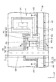
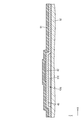
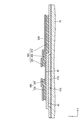
- a resist (photoresist) is applied to the upper layer side of the semiconductor film 42, the source conductive film 46S, and the drain conductive film 46D, and the resist is applied to a predetermined photomask. Then, after the exposed resist is developed, a patterned resist 53R (resist pattern) is formed as shown in FIGS. As shown in FIG. 5, the resist 53R covers the semiconductor film 42, the source conductive film 46S, and the drain conductive film 46D. In the plan view of FIG. 5, the patterned resist 53R is indicated by thin shading, and the peripheral edge of the resist 53R is indicated by a two-dot chain line.
- the resist 53R follows the shape of the semiconductor film 42, the source conductive film 46S, and the drain conductive film 46D in the plan view shown in FIG.
- the resist 53R has a shape that is slightly larger than the source conductive film 46S and the drain conductive film 46D in plan view.
- the distance L1 from the peripheral edge of the source conductive film 46S (or the drain conductive film 46D) to the peripheral edge of the resist 53R is set to 1 ⁇ m, for example, but is not limited to this value and can be changed as appropriate.
- the resist 53R is provided in such a way as to avoid a portion where a short circuit may occur due to the generation of the residue 51A in the stepped portion 45A extending along the peripheral edge of the gate conductive film 43G.
- the resist 53R is formed so as to avoid the three extending portions 45B, 45D, and 45E in the stepped portion 45A.
- the extending portion 45B has a portion (L-shaped portion) extending over both the source conductive film 46S and the drain conductive film 46D connected through the semiconductor film 42 in the stepped portion 45A. Part).
- the extending portion 45D is a portion extending over both of the two adjacent source conductive films 46S in the stepped portion 45A.
- the extending portion 45E (opposite side extending portion) includes the drain conductive film 46D and the drain conductive film 46D (for example, reference numeral 46D1 in FIG. 4) of the stepped portion 45A through the semiconductor film 42. This is a part extending over both of the source conductive films 46S (for example, reference numeral 46S1 in FIG. 4) on the side not connected.
- the source conductive film 46S1 corresponds to the drain conductive film 46D out of the two source conductive films 46S arranged with the drain conductive film 46D interposed therebetween.
- the resist 53R may be arranged so as to avoid at least a part of the extending portion 45B in the extending direction. In other words, it suffices that a part of the peripheral end portion of the resist 53R is arranged so as to intersect the extending portion 45B.
- the residue 51A can be cut in the second etching step described later.
- the extending portions 45D and 45E may be arranged such that the resist 53R avoids at least a part of the extending portions 45D and 45E in the extending direction.
- etching that can remove the conductive film 51 is performed using the resist 53R as a mask.
- the same type of etching as that performed in the first etching step is performed, but the present invention is not limited to this.
- the residue 51A of the stepped portion 45A is removed.
- the resist 53R is stripped through a resist stripping step after finishing the first etching step.
- etching is performed until a part 45F (indicated by a two-dot chain line in FIG. 13) of the gate insulating film 45 is removed, so that the residue 51A of the conductive film 51 is more reliably removed. can do.
- a conductive film forming step for forming the conductive film 51 so as to cover both the films 42 and a source electrode 38S connected to the semiconductor film 42 by etching the conductive film 51 are performed after the conductive film forming step.
- the first etching process for forming the source conductive film 46S and the drain conductive film 46D having the drain electrode 39D connected to the semiconductor film 42, and the semiconductor film 42, the source conductive film are performed after the first etching process.
- the resist 53R as a mask comprises a second etching step for removable etch the conductive film 51.
- a stepped portion 45 ⁇ / b> A is generated at a location overlapping the peripheral end portion of the gate electrode 37 ⁇ / b> G and a location overlapping the peripheral end portion of the gate wiring 35 ⁇ / b> G due to the thickness of the gate electrode 37 ⁇ / b> G and the gate wiring 35 ⁇ / b> G.
- the source conductive film 46S and the drain conductive film 46D are formed on the gate insulating film 45 by etching, the conductive film 51 is hardly removed at the stepped portion 45A of the gate insulating film 45, and the residue 51A of the conductive film 51 is removed. There is concern about the situation that will occur.
- a resist 53R is formed to cover the semiconductor film 42, the source conductive film 46S, and the drain conductive film 46D.
- Etching capable of removing the conductive film 51 is performed (second etching step). For this reason, even if the conductive film 51 remains in the step portion 45A of the gate insulating film 45, it can be removed.
- the semiconductor film 42 is covered with the resist 53R, the semiconductor film 42 can be protected from etching.
- the resist 45 avoids at least a part of the extending portion 45B extending over both the source conductive film 46S and the drain conductive film 46D among the stepped portions 45A formed in the gate insulating film 45. 53R is formed.
- the resist 53R is formed avoiding at least a part of the extended portion 45B. Thereby, even if the residue 51A connecting the conductive film 46S for the source and the conductive film 46D for the drain is generated in the extended portion 45B, the residue 51A can be removed (cut) in the second etching step. A situation in which the source electrode 38S and the drain electrode 39D are electrically connected through the residue 51A can be suppressed.
- a plurality of source conductive films 46S and drain conductive films 46D are formed along the extending direction of the gate wiring 35G, and in the resist forming process, they are formed on the gate insulating film 45.
- the resist 53R can be formed avoiding at least a part of the extended portion 45D extending over both of the two adjacent source conductive films 46S.
- the residue 51A of the conductive film 51 generated between the two adjacent source conductive films 46S in the second etching step can be removed, and the two adjacent source conductive films 46S pass through the residue 51A of the conductive film 51.
- the situation where it is electrically connected can be suppressed.
- a plurality of source conductive films 46S and drain conductive films 46D are formed along the extending direction of the gate wiring 35G, and the drain conductive film 46D is interposed therebetween.
- the source conductive film 46S disposed on the opposite side of the source conductive film 46S connected to the drain conductive film 46D via the semiconductor film 42 is used as the source conductive film.
- the film 46S1 in the resist formation step at least one of the extended portions 45E extending over both the drain conductive film 46D and the source conductive film 46S1 among the stepped portions 45A formed in the gate insulating film 45.
- the resist 53R is formed avoiding the portion.
- the residue 51A connecting the drain conductive film 46D and the source conductive film 46S1 can be removed in the second etching step, and the drain conductive film 46D and the source conductive film 46S1. Can be prevented from being electrically connected through the residue 51A of the conductive film 51.
- a resist 53R having a shape that follows the shape of the source conductive film 46S and the drain conductive film 46D is formed.
- the source conductive film 46S and the drain conductive film 46D can be removed at substantially the same locations as those removed in the first etching step.
- overetching is generally performed in order to reliably remove unnecessary conductive films.
- the etching time in the first etching step (more specifically, the time for performing overetching) can be reduced, and etching for the reduced time can be performed in the second etching step.
- the gate electrode 37G and the gate wiring 35G include aluminum.
- aluminum has a higher electrical resistance than copper. Therefore, when aluminum is used for the gate electrode 37G and the gate wiring 35G, it is preferable to make the gate electrode 37G and the gate wiring 35G thicker than when copper is used in order to reduce electrical resistance.
- the gate electrode 37G and the gate wiring 35G are thickened, the height of the stepped portion 45A of the gate insulating film 45 resulting from the thickness of the gate electrode 37G and the gate wiring 35G also increases, so that the residue 51A of the conductive film 51 is more likely to occur. Become. In the present embodiment, since the residue 51A of the conductive film 51 can be removed in the second etching step, it is particularly suitable when aluminum is used for the gate electrode 37G and the gate wiring 35G.
- Embodiment 2 of the present invention will be described with reference to FIG.
- the formation range of the resist formed in the second resist forming step is different from that of the above embodiment. Note that the same portions as those in the above embodiment are denoted by the same reference numerals and redundant description is omitted.
- the resist 153R resist pattern, thin shaded portion in FIG. 15
- the second resist forming step of the present embodiment is formed over the entire display area A1 in the array substrate 30. And has two types of openings 154 and 155. For example, one opening 154, 155 is provided for each pixel 19, but the present invention is not limited to this.
- the opening 154 has a rectangular shape in a plan view and is arranged so as to intersect with the extending portion 45B in the stepped portion 45A.
- the opening 154 is formed in order to remove the residue 51A of the conductive film 51 generated in the extending portion 45B.
- the opening 155 has a rectangular shape in a plan view and is arranged so as to intersect with both the extending portions 45D and 45E in the stepped portion 45A.
- the opening 155 is formed in order to remove the residue 51A of the conductive film 51 generated in the extending portions 45D and 45E.
- the shape of the openings 154 and 155 is not limited to a rectangle and can be changed as appropriate.
- the resist 153R is configured to cover portions other than the openings 154 and 155 in the display area A1.
- the resist 153R covers the gate insulating film 45, the source conductive film 46S, the gate conductive film 43G, the drain conductive film 46D, and the semiconductor film 42, and may cause a short circuit between the conductive films due to the residue 51A.
- the structure is not covered.
- By performing the second etching step using such a resist 153R as a mask a part of the residue 51A generated in each of the extending portions 45B, 45D, 45E can be removed. That is, the residue 51A extending between the conductive films can be cut. Since the gate insulating film 45 is covered with the resist 153R, the situation where it is removed in the second etching step can be suppressed.
- the present invention is not limited to the embodiments described with reference to the above description and drawings.
- the following embodiments are also included in the technical scope of the present invention.
- (1) the liquid crystal panel whose planar shape is rectangular has been exemplified.
- the present invention can also be applied to a liquid crystal panel whose planar shape is square, circular, elliptical, or the like.
- (2) In each of the above-described embodiments, the case where the driver is COG-mounted on the array substrate of the liquid crystal panel is shown. However, the driver is configured to be mounted on the flexible substrate by COF (Chip On Film). Also good.
- COF Chip On Film
- the semiconductor film constituting the channel portion of the TFT is made of an oxide semiconductor material
- polysilicon polycrystallized silicon (polycrystal It is also possible to use CG silicon (Continuous Grain Silicon)) which is a kind of silicon) or amorphous silicon as a material for the semiconductor film.
- CG silicon Continuous Grain Silicon
- amorphous silicon a material for the semiconductor film.
- the liquid crystal panel in which the operation mode is set to the FFS mode is illustrated, but other than that, there are other modes such as an IPS (In-Plane Switching) mode and a VA (Vertical Alignment) mode
- the present invention can also be applied to a liquid crystal panel in the operation mode.
- the color filter of the liquid crystal panel is exemplified as a three-color configuration of red, green and blue.
- a yellow colored portion is added to each colored portion of red, green and blue.
- the present invention can also be applied to a color filter having a four-color configuration.
- the material of the conductive film 51 is not limited to that described above, and can be changed as appropriate.
- a metal film such as chromium (Cr), tantalum (Ta), or copper (Cu) can be used in addition to aluminum and titanium, and these metal films may be stacked.
- the configuration in which the resist 53R formed in the second resist forming step is slightly larger than the source conductive film 46S and the drain conductive film 46D in plan view is illustrated.
- the resist 53R may have a shape that completely matches the shapes of the source conductive film 46S and the drain conductive film 46D in plan view.
- the shapes (formation ranges) of the gate conductive film 43G, the source conductive film 46S, and the drain conductive film 46D are not limited to those illustrated in the above embodiment, and can be changed as appropriate.
Landscapes
- Physics & Mathematics (AREA)
- Nonlinear Science (AREA)
- Engineering & Computer Science (AREA)
- Microelectronics & Electronic Packaging (AREA)
- Mathematical Physics (AREA)
- Chemical & Material Sciences (AREA)
- Crystallography & Structural Chemistry (AREA)
- General Physics & Mathematics (AREA)
- Optics & Photonics (AREA)
- Liquid Crystal (AREA)
- Manufacturing & Machinery (AREA)
- Thin Film Transistor (AREA)
Abstract
L'invention concerne un procédé de fabrication d'un substrat pour un panneau d'affichage, caractérisé en ce qu'il comprend une étape de formation de film conducteur destinée à former un film conducteur de façon à recouvrir à la fois un film d'isolation de gâchette (45A), etc. formé sur un substrat en verre et recouvrant une électrode de gâchette (37G) et un fil de gâchette (35G), et un film semiconducteur (42) formé sur un emplacement recouvrant l'électrode de gâchette (37G) sur le film d'isolation de gâchette (45A), etc.; une première étape de gravure destinée à former, par gravure de films conducteurs, un film conducteur (46S) pour une source connectée au film semiconducteur (42) et un film conducteur (46D) pour un drain connecté au film semiconducteur (42) ; une étape de formation de réserve destinée à former une réserve (53R) recouvrant le film semiconducteur (42), le film conducteur (46S) pour une source et le film conducteur (46D) pour un drain, exécutée après la première étape de gravure ; et une deuxième étape de gravure destinée à graver de façon amovible un film conducteur (51A) en utilisant la réserve (53R) comme masque, exécutée après l'étape de formation de réserve.
Priority Applications (2)
| Application Number | Priority Date | Filing Date | Title |
|---|---|---|---|
| US16/078,280 US10497725B2 (en) | 2016-02-26 | 2017-02-17 | Method of producing display panel board |
| CN201780013382.3A CN108701432B (zh) | 2016-02-26 | 2017-02-17 | 显示面板用基板的制造方法 |
Applications Claiming Priority (2)
| Application Number | Priority Date | Filing Date | Title |
|---|---|---|---|
| JP2016035388 | 2016-02-26 | ||
| JP2016-035388 | 2016-02-26 |
Publications (1)
| Publication Number | Publication Date |
|---|---|
| WO2017145941A1 true WO2017145941A1 (fr) | 2017-08-31 |
Family
ID=59686112
Family Applications (1)
| Application Number | Title | Priority Date | Filing Date |
|---|---|---|---|
| PCT/JP2017/005941 Ceased WO2017145941A1 (fr) | 2016-02-26 | 2017-02-17 | Procédé de fabrication d'un substrat pour panneau d'affichage |
Country Status (3)
| Country | Link |
|---|---|
| US (1) | US10497725B2 (fr) |
| CN (1) | CN108701432B (fr) |
| WO (1) | WO2017145941A1 (fr) |
Families Citing this family (1)
| Publication number | Priority date | Publication date | Assignee | Title |
|---|---|---|---|---|
| CN111106134B (zh) * | 2018-10-29 | 2023-08-08 | 夏普株式会社 | 有源矩阵基板以及具备其的x射线拍摄面板 |
Citations (4)
| Publication number | Priority date | Publication date | Assignee | Title |
|---|---|---|---|---|
| JPH10161158A (ja) * | 1996-11-29 | 1998-06-19 | Lg Electron Inc | 液晶表示装置及びその製造方法 |
| US20050250270A1 (en) * | 2004-05-06 | 2005-11-10 | Ying-Ming Wu | Process of manufacturing thin film transistor |
| JP2010097212A (ja) * | 2008-09-19 | 2010-04-30 | Semiconductor Energy Lab Co Ltd | 表示装置およびその作製方法 |
| JP2011054951A (ja) * | 2009-08-07 | 2011-03-17 | Semiconductor Energy Lab Co Ltd | 半導体装置およびその作製方法 |
Family Cites Families (8)
| Publication number | Priority date | Publication date | Assignee | Title |
|---|---|---|---|---|
| TW428256B (en) * | 1999-01-25 | 2001-04-01 | United Microelectronics Corp | Structure of conducting-wire layer and its fabricating method |
| JP2004014888A (ja) * | 2002-06-10 | 2004-01-15 | Mitsui Mining & Smelting Co Ltd | プリント配線板の製造方法及びその製造方法で得られたプリント配線板 |
| KR20070075808A (ko) * | 2006-01-16 | 2007-07-24 | 삼성전자주식회사 | 표시 기판의 제조 방법 및 이를 이용하여 제조한 표시 기판 |
| JP5527966B2 (ja) * | 2007-12-28 | 2014-06-25 | 株式会社半導体エネルギー研究所 | 薄膜トランジスタ |
| CN101833204A (zh) * | 2009-03-13 | 2010-09-15 | 北京京东方光电科技有限公司 | 阵列基板及其制造方法和液晶面板 |
| EP2518772A4 (fr) * | 2009-12-21 | 2016-09-07 | Sharp Kk | Substrat de matrice active, panneau d'affichage doté d'un tel substrat de matrice active et procédé de fabrication dudit substrat |
| JP2011151194A (ja) | 2010-01-21 | 2011-08-04 | Hitachi Displays Ltd | 液晶表示装置及びその製造方法 |
| CN104347772B (zh) * | 2014-09-30 | 2017-06-20 | 山东成林光电技术有限责任公司 | Ito的完整蚀刻方法及led芯片制作方法 |
-
2017
- 2017-02-17 WO PCT/JP2017/005941 patent/WO2017145941A1/fr not_active Ceased
- 2017-02-17 CN CN201780013382.3A patent/CN108701432B/zh active Active
- 2017-02-17 US US16/078,280 patent/US10497725B2/en active Active
Patent Citations (4)
| Publication number | Priority date | Publication date | Assignee | Title |
|---|---|---|---|---|
| JPH10161158A (ja) * | 1996-11-29 | 1998-06-19 | Lg Electron Inc | 液晶表示装置及びその製造方法 |
| US20050250270A1 (en) * | 2004-05-06 | 2005-11-10 | Ying-Ming Wu | Process of manufacturing thin film transistor |
| JP2010097212A (ja) * | 2008-09-19 | 2010-04-30 | Semiconductor Energy Lab Co Ltd | 表示装置およびその作製方法 |
| JP2011054951A (ja) * | 2009-08-07 | 2011-03-17 | Semiconductor Energy Lab Co Ltd | 半導体装置およびその作製方法 |
Also Published As
| Publication number | Publication date |
|---|---|
| US10497725B2 (en) | 2019-12-03 |
| CN108701432A (zh) | 2018-10-23 |
| CN108701432B (zh) | 2021-02-26 |
| US20190051678A1 (en) | 2019-02-14 |
Similar Documents
| Publication | Publication Date | Title |
|---|---|---|
| JP4619997B2 (ja) | 液晶表示装置とその製造方法 | |
| US10288965B2 (en) | Method for producing semiconductor device for high definition | |
| JP5336102B2 (ja) | Tft基板 | |
| US7733453B2 (en) | Method of fabricating a liquid crystal display device using a three mask process and double layer electrodes | |
| TWI579624B (zh) | 邊緣電場切換型液晶顯示裝置用陣列基板及其製造方法 | |
| KR100905409B1 (ko) | 액정표시장치 및 그 제조방법 | |
| JP5280988B2 (ja) | 液晶表示装置の製造方法 | |
| KR100995020B1 (ko) | 액정표시장치 및 그 제조방법 | |
| KR20150078248A (ko) | 표시소자 | |
| KR20010109491A (ko) | 컬러액정표시장치 및 그 제조방법 | |
| WO2017077994A1 (fr) | Substrat d'affichage, et dispositif d'affichage | |
| WO2017077995A1 (fr) | Substrat d'affichage ainsi que procédé de fabrication de celui-ci, et dispositif d'affichage | |
| JP2008165242A (ja) | 液晶表示装置及びその製造方法 | |
| WO2017077997A1 (fr) | Substrat d'affichage, et dispositif d'affichage | |
| US9989828B2 (en) | Semiconductor device and liquid crystal display device | |
| JP5048914B2 (ja) | 薄膜トランジスタ表示板の製造方法 | |
| KR101898624B1 (ko) | 프린지 필드형 액정표시장치 및 그의 제조방법 | |
| KR101758834B1 (ko) | 횡전계형 액정표시장치용 어레이 기판 및 이의 제조 방법 | |
| KR101969429B1 (ko) | 에프에프에스 방식 액정표시장치용 어레이기판 및 그 제조방법 | |
| KR20130033676A (ko) | 프린지 필드 스위칭 모드 액정표시장치 | |
| US20190081076A1 (en) | Thin film transistor substrate and display panel | |
| KR20130027207A (ko) | 액정표시장치용 어레이 기판의 제조방법 | |
| KR101886861B1 (ko) | 게이트 인 패널 구조 표시장치용 어레이 기판 및 이의 제조 방법 | |
| WO2017145941A1 (fr) | Procédé de fabrication d'un substrat pour panneau d'affichage | |
| KR102438251B1 (ko) | 액정표시장치 및 그 제조방법 |
Legal Events
| Date | Code | Title | Description |
|---|---|---|---|
| NENP | Non-entry into the national phase |
Ref country code: DE |
|
| 121 | Ep: the epo has been informed by wipo that ep was designated in this application |
Ref document number: 17756380 Country of ref document: EP Kind code of ref document: A1 |
|
| 122 | Ep: pct application non-entry in european phase |
Ref document number: 17756380 Country of ref document: EP Kind code of ref document: A1 |
|
| NENP | Non-entry into the national phase |
Ref country code: JP |