WO2017149607A1 - Dispositif à semi-conducteurs - Google Patents
Dispositif à semi-conducteurs Download PDFInfo
- Publication number
- WO2017149607A1 WO2017149607A1 PCT/JP2016/056087 JP2016056087W WO2017149607A1 WO 2017149607 A1 WO2017149607 A1 WO 2017149607A1 JP 2016056087 W JP2016056087 W JP 2016056087W WO 2017149607 A1 WO2017149607 A1 WO 2017149607A1
- Authority
- WO
- WIPO (PCT)
- Prior art keywords
- type
- layer
- type cathode
- cathode layer
- impurity concentration
- Prior art date
- Legal status (The legal status is an assumption and is not a legal conclusion. Google has not performed a legal analysis and makes no representation as to the accuracy of the status listed.)
- Ceased
Links
Images


Classifications
-
- H—ELECTRICITY
- H10—SEMICONDUCTOR DEVICES; ELECTRIC SOLID-STATE DEVICES NOT OTHERWISE PROVIDED FOR
- H10D—INORGANIC ELECTRIC SEMICONDUCTOR DEVICES
- H10D8/00—Diodes
-
- H—ELECTRICITY
- H10—SEMICONDUCTOR DEVICES; ELECTRIC SOLID-STATE DEVICES NOT OTHERWISE PROVIDED FOR
- H10D—INORGANIC ELECTRIC SEMICONDUCTOR DEVICES
- H10D62/00—Semiconductor bodies, or regions thereof, of devices having potential barriers
- H10D62/10—Shapes, relative sizes or dispositions of the regions of the semiconductor bodies; Shapes of the semiconductor bodies
- H10D62/124—Shapes, relative sizes or dispositions of the regions of semiconductor bodies or of junctions between the regions
- H10D62/125—Shapes of junctions between the regions
-
- H—ELECTRICITY
- H10—SEMICONDUCTOR DEVICES; ELECTRIC SOLID-STATE DEVICES NOT OTHERWISE PROVIDED FOR
- H10D—INORGANIC ELECTRIC SEMICONDUCTOR DEVICES
- H10D62/00—Semiconductor bodies, or regions thereof, of devices having potential barriers
- H10D62/10—Shapes, relative sizes or dispositions of the regions of the semiconductor bodies; Shapes of the semiconductor bodies
- H10D62/128—Anode regions of diodes
-
- H—ELECTRICITY
- H10—SEMICONDUCTOR DEVICES; ELECTRIC SOLID-STATE DEVICES NOT OTHERWISE PROVIDED FOR
- H10D—INORGANIC ELECTRIC SEMICONDUCTOR DEVICES
- H10D62/00—Semiconductor bodies, or regions thereof, of devices having potential barriers
- H10D62/10—Shapes, relative sizes or dispositions of the regions of the semiconductor bodies; Shapes of the semiconductor bodies
- H10D62/129—Cathode regions of diodes
-
- H—ELECTRICITY
- H10—SEMICONDUCTOR DEVICES; ELECTRIC SOLID-STATE DEVICES NOT OTHERWISE PROVIDED FOR
- H10D—INORGANIC ELECTRIC SEMICONDUCTOR DEVICES
- H10D62/00—Semiconductor bodies, or regions thereof, of devices having potential barriers
- H10D62/60—Impurity distributions or concentrations
-
- H—ELECTRICITY
- H10—SEMICONDUCTOR DEVICES; ELECTRIC SOLID-STATE DEVICES NOT OTHERWISE PROVIDED FOR
- H10D—INORGANIC ELECTRIC SEMICONDUCTOR DEVICES
- H10D62/00—Semiconductor bodies, or regions thereof, of devices having potential barriers
- H10D62/80—Semiconductor bodies, or regions thereof, of devices having potential barriers characterised by the materials
- H10D62/83—Semiconductor bodies, or regions thereof, of devices having potential barriers characterised by the materials being Group IV materials, e.g. B-doped Si or undoped Ge
- H10D62/8303—Diamond
-
- H—ELECTRICITY
- H10—SEMICONDUCTOR DEVICES; ELECTRIC SOLID-STATE DEVICES NOT OTHERWISE PROVIDED FOR
- H10D—INORGANIC ELECTRIC SEMICONDUCTOR DEVICES
- H10D62/00—Semiconductor bodies, or regions thereof, of devices having potential barriers
- H10D62/80—Semiconductor bodies, or regions thereof, of devices having potential barriers characterised by the materials
- H10D62/83—Semiconductor bodies, or regions thereof, of devices having potential barriers characterised by the materials being Group IV materials, e.g. B-doped Si or undoped Ge
- H10D62/832—Semiconductor bodies, or regions thereof, of devices having potential barriers characterised by the materials being Group IV materials, e.g. B-doped Si or undoped Ge being Group IV materials comprising two or more elements, e.g. SiGe
- H10D62/8325—Silicon carbide
-
- H—ELECTRICITY
- H10—SEMICONDUCTOR DEVICES; ELECTRIC SOLID-STATE DEVICES NOT OTHERWISE PROVIDED FOR
- H10D—INORGANIC ELECTRIC SEMICONDUCTOR DEVICES
- H10D62/00—Semiconductor bodies, or regions thereof, of devices having potential barriers
- H10D62/80—Semiconductor bodies, or regions thereof, of devices having potential barriers characterised by the materials
- H10D62/85—Semiconductor bodies, or regions thereof, of devices having potential barriers characterised by the materials being Group III-V materials, e.g. GaAs
- H10D62/8503—Nitride Group III-V materials, e.g. AlN or GaN
Definitions
- the present invention relates to a semiconductor device.
- V F -E REC the variation in V F -E REC is large depending on the irradiation angle or temperature with the irradiated object during electron / ion irradiation.
- problems such as fluctuations in electrical characteristics due to changes in lattice defects due to self-heating during chip energization operation, and thermal runaway during high temperature operation due to large leakage current caused by lattice defects.
- the present invention has been made to solve the above-described problems, and an object of the present invention is to obtain a semiconductor device capable of adjusting the V F -E REC trade-off characteristics without relying on lifetime control. .
- the semiconductor device includes a drift layer, first and second p-type anode layers formed side by side on the drift layer, and an n-type formed side by side under the drift layer.
- the diffusion depth of the first p-type anode layer is deeper than the diffusion depth of the second p-type anode layer, and the impurity concentration of the first p-type anode layer is the impurity concentration of the second p-type anode layer.
- the diffusion depth of the n-type cathode layer is larger than the diffusion depth of the p-type cathode layer, and the impurity concentration of the n-type cathode layer is larger than the impurity concentration of the p-type cathode layer.
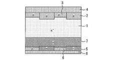
- FIG. 1 is a cross-sectional view showing a semiconductor device according to the first embodiment of the present invention.
- First and second p-type anode layers 2 and 3 are formed side by side on the n ⁇ -type drift layer 1.
- the anode electrode 4 is connected in ohmic contact with the first and second p-type anode layers 2 and 3.
- An n-type cathode layer 5 and a p-type cathode layer 6 are formed side by side under the n ⁇ -type drift layer 1.
- An n-type buffer layer 7 is formed between the n ⁇ -type drift layer 1 and the n-type cathode layer 5 and the p-type cathode layer 6.
- the cathode electrode 8 is connected so as to make ohmic contact with the n-type cathode layer 5 and the p-type cathode layer 6.
- the n-type cathode layer 5 and the p-type cathode layer 6 are short-circuited through the cathode electrode 8.
- the diffusion depth xp2 of the first p-type anode layer 2 is deeper than the diffusion depth xp3 of the second p-type anode layer 3 (xp2> xp3).
- the impurity concentration cp2 of the first p-type anode layer 2 is larger than the impurity concentration cp3 of the second p-type anode layer 3 (cp2> cp3).
- the diffusion depth xn2 of the n-type cathode layer 5 is deeper than the diffusion depth xp1 of the p-type cathode layer 6 (xn2> xp1).
- the impurity concentration cn2 of the n-type cathode layer 5 is larger than the impurity concentration cp1 of the p-type cathode layer 6 (cn2> cp1).
- V F is increased, E REC decreases. That is, the V F -E REC trade-off curve shifts to the high speed side. Therefore, it is desirable that the V F -E REC trade-off characteristic can be adjusted by changing the back surface p / n pitch as a free wheel diode incorporated in an inverter suitable for various applications.
- the back surface p / n pitch is designed too small, the snap-off resistance decreases, and conversely, if the design is too large, the recovery resistance decreases.
- the contradiction can be avoided by setting the diffusion depth and impurity concentration as in the present embodiment.
- V F is increased, E REC decreases. That is, the V F -E REC trade-off curve shifts to the high speed side. Therefore, it is desirable that the V F -E REC trade-off characteristics can be adjusted by changing the back surface p / n short ratio as a free wheel diode incorporated in an inverter suitable for various applications.
- the back surface p / n short ratio is designed too small, the snap-off resistance decreases, the cross point increases, and conversely if too large, the recovery resistance decreases.
- the contradiction can be avoided by designing the anode structure as in the present embodiment.
- V F concentration of the p-type anode layer
- E REC decreases. That is, the V F -E REC trade-off curve shifts to the high speed side.
- the Irr of the recovery waveform is lowered by decreasing the carrier concentration on the anode side in the ON state, and the snap-off resistance can be improved by relatively increasing the carrier concentration on the cathode side.
- the concentration of the p-type anode layer is lowered too much, the breakdown voltage is lowered.
- the contradiction can be avoided by designing the anode structure as in the present embodiment.
- the V F -E REC trade-off characteristic can be adjusted over a wide range without relying on conventional lifetime control. For this reason, the snap-off phenomenon in which the voltage jumps at the end of the turn-off operation and the oscillation phenomenon triggered by the phenomenon can be suppressed. And the interruption
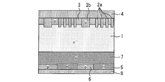
- FIG. FIG. 2 is a sectional view showing a semiconductor device according to the second embodiment of the present invention.
- the pitch of the first p-type anode layer 2 is smaller than the pitch of the n-type cathode layer 5.
- the maximum cut-off current density at the time of recovery is lower than in a diode without such a structure.
- the pitch of the first p-type anode layer 2 as in the present embodiment, it is possible to suppress the operation of the parasitic parasitic bipolar transistor in the vertical direction. A decrease in current density can be suppressed.
- the same effects as those of the first embodiment can be obtained.
- FIG. 3 is a cross-sectional view showing a semiconductor device according to Embodiment 3 of the present invention.
- the pitch of the first p-type anode layer 2 a on the n-type cathode layer 5 is smaller than the pitch of the first p-type anode layer 2 b on the p-type cathode layer 6.
- the operation of the parasitic bipolar transistor in the vertical direction can be suppressed, so that a decrease in the maximum controllable current density during recovery can be suppressed.
- the same effects as those of the first embodiment can be obtained.
- FIG. 4 is a sectional view showing a semiconductor device according to the fourth embodiment of the present invention.
- the pitch of one cycle composed of the first p-type anode layer 2 and the second p-type anode layer 3 is smaller than the pitch of one cycle composed of the n-type cathode layer 5 and the p-type cathode layer 6.
- the operation of the parasitic bipolar transistor in the vertical direction can be suppressed, so that a decrease in the maximum controllable current density during recovery can be suppressed.
- the same effects as those of the first embodiment can be obtained.
- the diode forming the high withstand voltage power module ( ⁇ 600 V) has been described as an example. And the above effects can be obtained.
- the semiconductor device is not limited to one formed of silicon, and may be formed of a wide band gap semiconductor having a larger band gap than silicon.
- the wide band gap semiconductor is, for example, silicon carbide, a gallium nitride-based material, or diamond.
- a power semiconductor element formed of such a wide band gap semiconductor can be miniaturized because of its high voltage resistance and allowable current density.
- a semiconductor module incorporating this element can also be miniaturized.
- the heat resistance of the element is high, the heat dissipating fins of the heat sink can be miniaturized and the water cooling part can be air cooled, so that the semiconductor module can be further miniaturized.
- the efficiency of the semiconductor module can be increased.
Landscapes
- Electrodes Of Semiconductors (AREA)
- Thyristors (AREA)
Abstract
Priority Applications (5)
| Application Number | Priority Date | Filing Date | Title |
|---|---|---|---|
| JP2018502874A JP6750668B2 (ja) | 2016-02-29 | 2016-02-29 | 半導体装置 |
| US15/766,114 US10355142B2 (en) | 2016-02-29 | 2016-02-29 | Semiconductor device |
| DE112016006517.5T DE112016006517B4 (de) | 2016-02-29 | 2016-02-29 | Halbleitervorrichtungen |
| CN201680082481.2A CN108701722B (zh) | 2016-02-29 | 2016-02-29 | 半导体装置 |
| PCT/JP2016/056087 WO2017149607A1 (fr) | 2016-02-29 | 2016-02-29 | Dispositif à semi-conducteurs |
Applications Claiming Priority (1)
| Application Number | Priority Date | Filing Date | Title |
|---|---|---|---|
| PCT/JP2016/056087 WO2017149607A1 (fr) | 2016-02-29 | 2016-02-29 | Dispositif à semi-conducteurs |
Publications (1)
| Publication Number | Publication Date |
|---|---|
| WO2017149607A1 true WO2017149607A1 (fr) | 2017-09-08 |
Family
ID=59742548
Family Applications (1)
| Application Number | Title | Priority Date | Filing Date |
|---|---|---|---|
| PCT/JP2016/056087 Ceased WO2017149607A1 (fr) | 2016-02-29 | 2016-02-29 | Dispositif à semi-conducteurs |
Country Status (5)
| Country | Link |
|---|---|
| US (1) | US10355142B2 (fr) |
| JP (1) | JP6750668B2 (fr) |
| CN (1) | CN108701722B (fr) |
| DE (1) | DE112016006517B4 (fr) |
| WO (1) | WO2017149607A1 (fr) |
Cited By (3)
| Publication number | Priority date | Publication date | Assignee | Title |
|---|---|---|---|---|
| JP2019096708A (ja) * | 2017-11-22 | 2019-06-20 | 三菱電機株式会社 | 半導体装置およびその製造方法 |
| US11004986B2 (en) | 2016-04-25 | 2021-05-11 | Mitsubishi Electric Corporation | Semiconductor device including adjacent semiconductor layers |
| JP2022048882A (ja) * | 2020-09-15 | 2022-03-28 | 株式会社東芝 | 半導体装置 |
Families Citing this family (1)
| Publication number | Priority date | Publication date | Assignee | Title |
|---|---|---|---|---|
| CN113728443B (zh) * | 2019-04-02 | 2024-04-05 | 日立能源有限公司 | 改进反向恢复的分段功率二极管结构 |
Citations (3)
| Publication number | Priority date | Publication date | Assignee | Title |
|---|---|---|---|---|
| JPS5637683A (en) * | 1979-09-04 | 1981-04-11 | Nippon Telegr & Teleph Corp <Ntt> | Semiconductor rectifying device |
| JP2014053451A (ja) * | 2012-09-07 | 2014-03-20 | Hitachi Power Semiconductor Device Ltd | ダイオード及び電力変換システム |
| WO2014199465A1 (fr) * | 2013-06-12 | 2014-12-18 | 三菱電機株式会社 | Appareil semiconducteur |
Family Cites Families (12)
| Publication number | Priority date | Publication date | Assignee | Title |
|---|---|---|---|---|
| GB2050694B (en) * | 1979-05-07 | 1983-09-28 | Nippon Telegraph & Telephone | Electrode structure for a semiconductor device |
| JPH0286173A (ja) | 1988-09-22 | 1990-03-27 | Fuji Electric Co Ltd | 半導体ダイオード |
| JP2851026B2 (ja) | 1993-10-05 | 1999-01-27 | 東洋電機製造株式会社 | 高速ダイオード |
| JPH1093113A (ja) * | 1996-09-19 | 1998-04-10 | Hitachi Ltd | ダイオード |
| JP2005243716A (ja) * | 2004-02-24 | 2005-09-08 | Sanyo Electric Co Ltd | 半導体装置 |
| US20070228505A1 (en) * | 2006-04-04 | 2007-10-04 | Mazzola Michael S | Junction barrier schottky rectifiers having epitaxially grown p+-n junctions and methods of making |
| WO2013014943A2 (fr) * | 2011-07-27 | 2013-01-31 | Kabushiki Kaisha Toyota Chuo Kenkyusho | Diode, dispositif à semi-conducteur et mosfet |
| JP2013235890A (ja) * | 2012-05-07 | 2013-11-21 | Denso Corp | 半導体装置 |
| US8843871B2 (en) * | 2012-06-29 | 2014-09-23 | Synopsys, Inc. | Estimating optimal gate sizes by using numerical delay models |
| KR20150123638A (ko) * | 2014-04-25 | 2015-11-04 | 삼성전기주식회사 | 반도체 소자 |
| JP6294175B2 (ja) * | 2014-07-02 | 2018-03-14 | 株式会社日立製作所 | 半導体装置およびそれを用いた電力変換システム |
| CN108028284B (zh) | 2015-09-25 | 2021-06-22 | 三菱电机株式会社 | 半导体装置 |
-
2016
- 2016-02-29 WO PCT/JP2016/056087 patent/WO2017149607A1/fr not_active Ceased
- 2016-02-29 DE DE112016006517.5T patent/DE112016006517B4/de active Active
- 2016-02-29 US US15/766,114 patent/US10355142B2/en active Active
- 2016-02-29 JP JP2018502874A patent/JP6750668B2/ja active Active
- 2016-02-29 CN CN201680082481.2A patent/CN108701722B/zh active Active
Patent Citations (3)
| Publication number | Priority date | Publication date | Assignee | Title |
|---|---|---|---|---|
| JPS5637683A (en) * | 1979-09-04 | 1981-04-11 | Nippon Telegr & Teleph Corp <Ntt> | Semiconductor rectifying device |
| JP2014053451A (ja) * | 2012-09-07 | 2014-03-20 | Hitachi Power Semiconductor Device Ltd | ダイオード及び電力変換システム |
| WO2014199465A1 (fr) * | 2013-06-12 | 2014-12-18 | 三菱電機株式会社 | Appareil semiconducteur |
Cited By (5)
| Publication number | Priority date | Publication date | Assignee | Title |
|---|---|---|---|---|
| US11004986B2 (en) | 2016-04-25 | 2021-05-11 | Mitsubishi Electric Corporation | Semiconductor device including adjacent semiconductor layers |
| JP2019096708A (ja) * | 2017-11-22 | 2019-06-20 | 三菱電機株式会社 | 半導体装置およびその製造方法 |
| JP2022048882A (ja) * | 2020-09-15 | 2022-03-28 | 株式会社東芝 | 半導体装置 |
| JP7410829B2 (ja) | 2020-09-15 | 2024-01-10 | 株式会社東芝 | 半導体装置 |
| US12125846B2 (en) | 2020-09-15 | 2024-10-22 | Kabushiki Kaisha Toshiba | Semiconductor device with complementary cathode regions |
Also Published As
| Publication number | Publication date |
|---|---|
| DE112016006517B4 (de) | 2022-09-29 |
| US20180315863A1 (en) | 2018-11-01 |
| DE112016006517T5 (de) | 2018-11-15 |
| CN108701722A (zh) | 2018-10-23 |
| US10355142B2 (en) | 2019-07-16 |
| JPWO2017149607A1 (ja) | 2018-10-04 |
| JP6750668B2 (ja) | 2020-09-02 |
| CN108701722B (zh) | 2021-06-11 |
Similar Documents
| Publication | Publication Date | Title |
|---|---|---|
| JP5971414B2 (ja) | 半導体装置 | |
| US9601485B2 (en) | Reverse-conducting IGBT with buffer layer and separation layer for reducing snapback | |
| JP6237915B2 (ja) | 半導体装置および半導体装置の製造方法 | |
| JP4843253B2 (ja) | 電力用半導体装置 | |
| JP6508099B2 (ja) | 半導体素子 | |
| JP6288315B2 (ja) | 半導体装置 | |
| US9202936B2 (en) | Semiconductor device | |
| JP2016195271A (ja) | 半導体装置 | |
| JP2009176892A (ja) | 半導体装置およびその製造方法 | |
| JP2019009288A (ja) | 半導体装置 | |
| CN113632238B (zh) | 半导体装置 | |
| JP6750668B2 (ja) | 半導体装置 | |
| JP5822032B2 (ja) | 半導体装置の製造方法 | |
| WO2021005903A1 (fr) | Dispositif à semi-conducteur au carbure de silicium et procédé de fabrication de dispositif à semi-conducteur au carbure de silicium | |
| JP6597826B2 (ja) | 半導体装置 | |
| WO2019049251A1 (fr) | Dispositif semiconducteur | |
| JP2014011285A (ja) | 半導体装置 |
Legal Events
| Date | Code | Title | Description |
|---|---|---|---|
| WWE | Wipo information: entry into national phase |
Ref document number: 15766114 Country of ref document: US |
|
| ENP | Entry into the national phase |
Ref document number: 2018502874 Country of ref document: JP Kind code of ref document: A |
|
| 121 | Ep: the epo has been informed by wipo that ep was designated in this application |
Ref document number: 16892452 Country of ref document: EP Kind code of ref document: A1 |
|
| 122 | Ep: pct application non-entry in european phase |
Ref document number: 16892452 Country of ref document: EP Kind code of ref document: A1 |