WO2017149649A1 - Carte de circuit imprimé électronique et dispositif de bobine - Google Patents
Carte de circuit imprimé électronique et dispositif de bobine Download PDFInfo
- Publication number
- WO2017149649A1 WO2017149649A1 PCT/JP2016/056221 JP2016056221W WO2017149649A1 WO 2017149649 A1 WO2017149649 A1 WO 2017149649A1 JP 2016056221 W JP2016056221 W JP 2016056221W WO 2017149649 A1 WO2017149649 A1 WO 2017149649A1
- Authority
- WO
- WIPO (PCT)
- Prior art keywords
- coil
- circuit board
- electronic circuit
- wiring board
- wiring
- Prior art date
- Legal status (The legal status is an assumption and is not a legal conclusion. Google has not performed a legal analysis and makes no representation as to the accuracy of the status listed.)
- Ceased
Links
Images




Classifications
-
- H—ELECTRICITY
- H01—ELECTRIC ELEMENTS
- H01F—MAGNETS; INDUCTANCES; TRANSFORMERS; SELECTION OF MATERIALS FOR THEIR MAGNETIC PROPERTIES
- H01F17/00—Fixed inductances of the signal type
- H01F17/04—Fixed inductances of the signal type with magnetic core
-
- H—ELECTRICITY
- H01—ELECTRIC ELEMENTS
- H01F—MAGNETS; INDUCTANCES; TRANSFORMERS; SELECTION OF MATERIALS FOR THEIR MAGNETIC PROPERTIES
- H01F27/00—Details of transformers or inductances, in general
- H01F27/06—Mounting, supporting, or suspending transformers, reactors, or choke coils not being of the signal type
-
- H—ELECTRICITY
- H01—ELECTRIC ELEMENTS
- H01F—MAGNETS; INDUCTANCES; TRANSFORMERS; SELECTION OF MATERIALS FOR THEIR MAGNETIC PROPERTIES
- H01F27/00—Details of transformers or inductances, in general
- H01F27/28—Coils; Windings; Conductive connections
- H01F27/29—Terminals; Tapping arrangements for signal inductances
Definitions
- the present invention relates to an electronic circuit board and a coil device, and more particularly to mounting of a coil for an electric device.
- the choke coil used as an electronic component such as a noise filter is used in various forms such as one having a large number of windings or one having a large number of wires, with the number of windings or the type of wire being determined according to the specifications.
- Patent Document 1 discloses a technique using a choke coil in which two thin windings are connected in parallel when the winding line becomes thick and winding is difficult, or when the coil size becomes large. ing.
- Patent Document 2 discloses a technique using a coil in which a plurality of windings are stacked and winding ends are connected in parallel.
- the present invention has been made in view of the above, and an object thereof is to obtain an electronic circuit board and a coil device that are easy to manufacture and highly reliable, reducing a load on a connection portion between a wiring board and a coil portion. .
- an electronic circuit board includes a plurality of conductive wires coated with insulation, a core having a magnetic material, and a plurality of conductive wires arranged in parallel to the core. And a coil substrate from which an end portion of the conductive wire is led out, and a wiring substrate including a wiring portion including a plurality of mounting portions in which the end portion of the conductive wire is divided and mounted for each single wire.
- the conductive wire is characterized in that each single wire is connected to an independent mounting portion.
- the present invention it is possible to reduce the load on the connection part between the wiring board and the coil part and to obtain an electronic circuit board that is easy to manufacture and highly reliable.
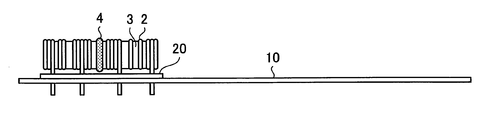
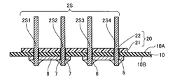
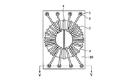
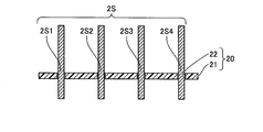
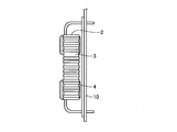
- FIG. Side view of essential parts of electronic circuit board of Embodiment 1 III-III sectional view of Fig. 1 The figure which shows the coil apparatus mounted in the electronic circuit board of Embodiment 1.
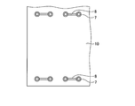
- FIG. V-V cross section of Fig. 4 The figure which shows the back surface of the wiring board in the electronic circuit board of Embodiment 1
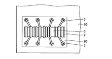
- FIG. Side view of electronic circuit board of Embodiment 2 The figure which shows the electronic circuit board of Embodiment 3.
- FIG. Side view of electronic circuit board of Embodiment 4 The figure which shows the electronic circuit board of Embodiment 5.
- FIG. 1 is a diagram showing a mounting state of a coil in which windings are arranged in parallel in the coil device for an electronic circuit board according to the first embodiment
- FIG. 2 is a side view of FIG. 3 is a cross-sectional view taken along the line III-III in FIG.
- FIG. 4 is a diagram illustrating a coil device for an electronic circuit board according to the first embodiment.
- the electronic circuit board 1 according to the first embodiment includes a printed circuit board as a wiring board 10 and a coil portion 2 around which a plurality of conductive wires 2 a coated with insulation are wound on the wiring board 10.
- a plurality of conductive wires 2a are arranged in parallel to the core 3, and end portions 2S (2S1, 2S2, 2S3, 2S4 and 2E1, 2E2, 2E3, 2E4) of the conductive wires 2a are derived.
- the core 3 is configured by a two-part annular body so that the conductive wire 2 a can be easily wound, and the divided part is fixed by the core support member 4.
- the wiring board 10 includes a mounting portion including a plurality of soldering portions 6 on which the end portions 2S of the four conductive wires 2a are mounted separately for each single wire, that is, for each conductive wire.
- the soldering portion 6 is formed on the second main surface 10 ⁇ / b> B of the wiring substrate 10.
- other electronic components and wiring patterns are formed on the electronic circuit board 1, but are not shown in FIG.
- the soldering part 6 shall mean the area
- the soldering part 6 as the mounting part is connected to the wiring board 10 through the through hole 5 penetrating from the front surface 10A, which is the first main surface on which the coil unit 2 is mounted, to the back surface 10B, which is the second main surface.
- a land 7 arranged on the second main surface 10B is formed.
- the coil device includes a coil portion 2 and an insulating plate 20 as shown in FIG.
- the ends 2S1, 2S2, 2S3, 2S4 of the conductive wire 2a of the coil part 2 are mounted via an insulating plate 20 between the surface 10A of the wiring board 10 as shown in FIG.
- the other end portions 2E1, 2E2, 2E3, and 2E4 of the conductive wire 2a of the coil portion 2 are also provided between the first main surface 10A of the wiring board 10 and the insulating plate 20 similarly to the one end side shown in FIG. Mounted through.
- the coil portion 2 is composed of a coil in which a conductive wire 2 a covered with insulation is used and windings are wound around the core 3 in parallel.
- the core 3 includes a magnetic body therein, has a two-part structure, and is housed in a case (not shown). That is, a case with an insulating coating having a semicircular donut shape is individually provided and integrated with the core support member 4.
- the insulating plate 20 is composed of a plate-like body 21 made of a resin substrate, and has a plurality of lead-out holes 22 spaced apart from each other, and the end 2S of the conductive wire 2a is independent for each single wire. Then, it is led to the soldering part 6 which is the mounting part on the wiring board 10 through the lead-out hole 22.
- the soldering portion 6 of the wiring board 10 connects two pads, that is, lands 7 by the wiring pattern 8, so that electrical connection is achieved.
- the electronic circuit board 1 according to the first embodiment is constituted by two kinds of members, that is, the coil part 2 and the wiring board 10 as shown in FIG.
- the coil device used in the electronic circuit board 1 according to the first embodiment includes a coil part that includes an insulating plate 20 made of an insulating material, for example, a resin material, on each of the windings in which the soldering part 6 to the wiring board 10 is arranged in parallel. 2 and the wiring board 10 and a plurality of lead-out holes 22 which are spaced apart from the insulating plate 20 and have a certain distance to end portions 2S (2S1, 2S2, 2S3, 2S4 and 2E1, 2E2, 2E3, 2E4) are derived, and the interval between the conductive lines 2a is defined.
- the insulating plate 20 By disposing the insulating plate 20 on the coil part 2, the mounting position on the wiring board 10 can be provided uniformly without depending on the winding position of the conductive wire 2a constituting the coil part 2.
- the second main surface 10 ⁇ / b> B which is the back surface of the wiring board 10 uses a wiring pattern 8 provided on the wiring board 10 in the same process as a circuit unit (not shown) for connection between the lands 7. That is, the lands 7 constituting the soldering portions 6 of the wiring board 10 provided at the same intervals as the through holes 5 of the coil portion 2 are connected by the wiring pattern 8.
- the coil has the shape of a common mode choke coil.
- the common mode choke coil is obtained by winding two series of conductive wires 2a around a core 3 having a magnetic material. Has a structure that is reversed.
- the coil device uses a pair of coils in which the winding direction of the coils is reversed when mounting the common mode choke coil. It is very easy to reverse the current direction of 2a. In other words, the normal mode choke coil and the common mode choke coil can be used without changing the coil part 2 itself, by simply changing the wiring pattern 8 for connecting the lands between the wiring boards 10. It is expensive.
- the coils can be easily connected in parallel or in series by simply changing the wiring pattern 8 between the lands 7. That is, two types of coil devices can be obtained by using a wiring board or an insulating plate having two types of wiring patterns 8.
- the insulating plate is formed using a resin substrate such as a glass epoxy substrate.
- the core 3 has a two-divided structure, and the case is also provided separately and integrated by the support member 4.
- the case is also provided separately and integrated by the support member 4.
- an integrated resin material case may be used.
- the coil device is obtained by individually inserting the end portion 2S of the conductive wire 2a of the coil portion 2 into the lead-out hole 22 of the insulating plate 20 and soldering as necessary. If necessary, the end 2S (2S1, 2S2, 2S3, 2S4 and 2E1, 2E2, 2S1, 2S2, 2S1, 2S2, and 2E2) of the conductive wire 2a of the coil device is inserted into the through hole 5 provided in the land of the wiring board 10 on which the wiring pattern and the circuit components are mounted. 2E3 and 2E4) are inserted and soldered to form the soldered portion 6. The solder reaches from the back surface 10B side to the front surface 10A side, and electrical and mechanical connections are made on the wiring board 10.
- the solder connection between the insulating plate 20 and the end portion 2S (2S1, 2S2, 2S3, 2S4 and 2E1, 2E2, 2E3, 2E4) of the conductive wire 2a may not be performed separately, and may be performed as necessary. Further, when the coil device is surface-mounted, the end 2S (2S1, 2S2, 2S3, 2S4 and 2E1, 2E2, 2E3, 2E4) of the conductive wire 2a is separated for each single wire by the lead-out hole 22 of the insulating plate 20 Therefore, if a reflow process of placing and heating on the wiring portion is performed, simultaneous mounting with other components is possible. As described above, since the conductive wire 2a is led out separately for each single wire in the lead-out hole 22 of the insulating plate 20, mounting on the wiring portion is particularly easy.
- the volume of the coil part per soldering part is reduced, so that the solder rise is improved and the time required for soldering can be reduced.
- the coil load is dispersed by increasing the number of connection portions with the wiring board, the load applied to the soldering portion can be reduced, and as a result, the rate of occurrence of solder cracks can be reduced.
- the state of poor soldering described here is a state in which the solder is not sufficiently supplied to a portion where the heat capacity of the soldering part is high, or a higher temperature and a longer heating time in order to supply a sufficient amount of solder. It is a state that requires.
- the coil device according to the first embodiment is applied to a coil having a large size and a heavy weight, so that not only the load of the soldering portion 6 but also the deflection of the substrate is affected. There is also a suppression effect, and the load on the board and peripheral components can be reduced.
- the above effect can be obtained by using the shape of the coil and the wiring pattern of the wiring board 10, this case does not significantly change the coil manufacturing method and the wiring board manufacturing method, and a new part is added. Since it is not necessary, it is technically easy and inexpensive.
- the coil portion 2 of the surface mount component may be mounted on the land 7 of the wiring substrate 10. Needless to say, it is effective.
- the connection between the lands 7 may be formed by forming a wiring pattern on the mounting surface side of the coil portion 2 or wiring on the back surface side through an appropriately provided through hole. You may make it carry out with a pattern.
- a wiring pattern for connecting lands may be formed on an insulating plate described later in the second embodiment.
- the land 7 of the soldering portion 6 of the wiring board 10 is connected at two points by the wiring pattern 8 so that electrical connection can be achieved.
- each soldering part of the paralleled coils is electrically connected, and can be handled equivalently to a single wire coil.
- the configuration of the coil part 2 and the soldering part 6 is in two rows, but the number of parallels can be changed to the number desired by the user by combining the coil shape and the shape of the soldering part of the wiring board. .
- the parallel number it is not necessary to arrange the soldering portions in a horizontal row, and the soldering portions can be freely arranged vertically and horizontally.
- FIG. FIG. 7 is a diagram showing the electronic circuit board of the second embodiment
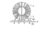
- FIG. 8 is a side view of the electronic circuit board of the second embodiment.
- the circular magnetic core 3 is described as being flat with respect to the wiring board 10.
- the core 3 is erected.
- a shaped coil portion 2 may be used. Since the configuration of the coil unit 2 itself is the same as that of the first embodiment, the description thereof is omitted here. The same symbols are assigned to the same members.
- the degree of freedom of wiring can be greatly increased, and a connection structure that is not unreasonable in terms of electrical and strength can be taken.
- the area occupied by the coil unit 2 on the wiring board 10 can be greatly reduced.
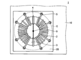
- FIG. 9 is a diagram illustrating an electronic circuit board according to the third embodiment.
- the soldered portion 6 of the coil portion 2 and the through holes 5 constituting the mounting holes of the wiring board 10 are arranged in two rows along the horizontal line. By changing the arrangement shape of 5, it is possible to obtain an effect of making the load on the soldering portion 6 more uniform.
- FIG. 9 shows a shape in which the through holes 5 formed in the coil part 2 and the soldering part 6 of the wiring board 10 are arranged at regular intervals on the same circumference C having a constant radius with respect to the center 9 of the magnetic core 3. It is. Since the configuration of the coil unit 2 itself is the same as that of the second embodiment, the description thereof is omitted here. The same symbols are assigned to the same members.
- the weight of the coil portion 2 can be evenly distributed to the mounting portion of the wiring board 10, and the load on the soldering portion can be further reduced as compared with the arrangement of the first embodiment.
- the influence on solder cracks can be reduced.
- the mounting portion on the wiring board 10 can be arranged with a sufficient distance, the heat capacity of the soldering portion can have the same level as in the first embodiment, so that the soldering can be performed. The time required can be reduced.
- FIG. 10 is a diagram showing an electronic circuit board according to the fourth embodiment
- FIG. 11 is a side view of the electronic circuit board according to the fourth embodiment.
- the mounting parts on the wiring board 10 are arranged so as to be evenly distributed.
- the electronic circuit board 1 shown in FIG. 10 when the coil is mounted on the wiring board 10 installed in the vertical direction, that is, perpendicular to the ground, as shown in FIG. It can also be made into the shape which gives a difference. Since the configuration of the coil unit 2 itself is the same as in the first and second embodiments, the description thereof is omitted here. The same symbols are assigned to the same members.
- the load applied to the soldering portion can be reduced as compared with the third embodiment by arranging the soldering portion so as to be biased in the coil portion up-down direction and the left-right direction.
- FIG. 12 is a diagram illustrating an electronic circuit board according to the fifth embodiment.
- the soldering portion is provided on the outer side with respect to the circular magnetic core 3, but as shown in FIG. A soldering portion is provided inside the magnetic core 3. Since other configurations are the same as those of the first embodiment, description thereof is omitted here.
- soldering portion can be fixed more firmly by providing a soldering portion inside the magnetic core 3.
- the soldering portion to be attached to the inside of the magnetic core 3 can be set to a shape desired by the designer, either by connecting two parallel coils in combination or by connecting only a single wire. Even when only a single wire is connected, electrical connection is achieved by wiring the wiring pattern of the wiring board 10 to the inside of the core 3 of the magnetic material. As a result, the load on the soldering portion can be reduced.
- FIG. FIG. 13 is a view showing the back surface of an insulating plate used in the electronic circuit board of the sixth embodiment.
- the wiring pattern 8 that connects the soldering portions is configured by the wiring pattern on the second main surface 10B side of the wiring board 10, but the electronic circuit board 1 of the sixth embodiment is made of glass epoxy.
- a land 27 and a wiring pattern 28 for connecting the lands are formed on the back surface of the insulating plate 20 made of a substrate. Since the configuration of the coil unit 2 itself is the same as that of the first embodiment, the description thereof is omitted here. The same symbols are assigned to the same members.
- the circuit configuration of the wiring board 10 can be freely formed without restriction, and more efficient circuit design is possible.
- the mounting portion on the wiring board is configured to be arranged independently for each winding, and the wiring pattern of the wiring board is formed.
- the load applied to each soldering part can be distributed while maintaining performance, and soldering can be performed by reducing the heat capacity of components because each wire can be mounted on a wiring board. This has the effect that the time required for the process can be reduced.
- an electronic circuit board that reduces the load on the soldering portion of the wiring board can be obtained at low cost without adding new components.
- a coil layer 2 is placed on the wiring substrate 10 or the insulating plate 20 by forming a solder layer in the region on the wiring substrate 10 or the region on the insulating plate 20 corresponding to each soldering portion.
- solder connection can be easily performed only by performing reflow.
- a single wire is used.
- one conductive wire includes a single integrated wire, and that each conductive wire is separated and soldered.
- the insulating plate is disposed between the coil portion and the wiring board, the insulating plate may be formed without being disposed.
- the configuration described in the above embodiment shows an example of the contents of the present invention, and can be combined with another known technique, and can be combined with other configurations without departing from the gist of the present invention. It is also possible to omit or change the part.
Landscapes
- Engineering & Computer Science (AREA)
- Power Engineering (AREA)
- Microelectronics & Electronic Packaging (AREA)
- Coils Or Transformers For Communication (AREA)
Abstract
Une carte de circuit imprimé électronique 1 selon la présente invention est pourvue : d'une pluralité de lignes conductrices 2a qui sont respectivement recouvertes de films isolants ; d'un noyau 3 ayant un corps magnétique ; d'une section de bobine 2, les lignes conductrices 2a étant enroulées parallèlement les unes aux autres sur le noyau 3, et les parties d'extrémité 2S des lignes conductrices 2a partant du noyau 3 ; et d'une carte de câblage 10 qui comporte une section de câblage comprenant une pluralité de sections de montage sur lesquelles les parties d'extrémité 2S des lignes conductrices 2a sont montées séparément par chaque ligne. Les lignes conductrices 2a sont connectées aux sections de montage indépendantes par chaque ligne. Avec la configuration susmentionnée, une charge sur une section de brasage 6, c'est-à-dire une section de connexion de la carte de câblage 10 avec la section de bobine 2, est réduite et une carte de circuit imprimé électronique 1 facile à fabriquer et très fiable peut être obtenue.
Priority Applications (3)
| Application Number | Priority Date | Filing Date | Title |
|---|---|---|---|
| JP2018502903A JP6602455B2 (ja) | 2016-03-01 | 2016-03-01 | 電子回路基板 |
| CN201690000361.9U CN207338056U (zh) | 2016-03-01 | 2016-03-01 | 电路基板以及线圈装置 |
| PCT/JP2016/056221 WO2017149649A1 (fr) | 2016-03-01 | 2016-03-01 | Carte de circuit imprimé électronique et dispositif de bobine |
Applications Claiming Priority (1)
| Application Number | Priority Date | Filing Date | Title |
|---|---|---|---|
| PCT/JP2016/056221 WO2017149649A1 (fr) | 2016-03-01 | 2016-03-01 | Carte de circuit imprimé électronique et dispositif de bobine |
Publications (1)
| Publication Number | Publication Date |
|---|---|
| WO2017149649A1 true WO2017149649A1 (fr) | 2017-09-08 |
Family
ID=59742640
Family Applications (1)
| Application Number | Title | Priority Date | Filing Date |
|---|---|---|---|
| PCT/JP2016/056221 Ceased WO2017149649A1 (fr) | 2016-03-01 | 2016-03-01 | Carte de circuit imprimé électronique et dispositif de bobine |
Country Status (3)
| Country | Link |
|---|---|
| JP (1) | JP6602455B2 (fr) |
| CN (1) | CN207338056U (fr) |
| WO (1) | WO2017149649A1 (fr) |
Cited By (2)
| Publication number | Priority date | Publication date | Assignee | Title |
|---|---|---|---|---|
| WO2022085317A1 (fr) * | 2020-10-19 | 2022-04-28 | 株式会社エス・エッチ・ティ | Bobine d'arrêt |
| WO2024189976A1 (fr) * | 2023-03-15 | 2024-09-19 | 三菱重工業株式会社 | Procédé de fabrication d'un composant de bobine, composant de bobine et produit intermédiaire |
Citations (4)
| Publication number | Priority date | Publication date | Assignee | Title |
|---|---|---|---|---|
| JPH0197523U (fr) * | 1987-12-19 | 1989-06-29 | ||
| JPH0235411U (fr) * | 1988-08-29 | 1990-03-07 | ||
| JPH0287609A (ja) * | 1988-09-26 | 1990-03-28 | Fujitsu Ltd | トロイダル型線輪体の実装方法 |
| WO2010052922A1 (fr) * | 2008-11-06 | 2010-05-14 | サンデン株式会社 | Compresseur électrique intégrant un onduleur |
Family Cites Families (5)
| Publication number | Priority date | Publication date | Assignee | Title |
|---|---|---|---|---|
| JPS61162021U (fr) * | 1985-03-27 | 1986-10-07 | ||
| JPH066488Y2 (ja) * | 1989-08-03 | 1994-02-16 | 株式会社安川電機 | 表面実装用小型チョークコイル装置 |
| JPH11233350A (ja) * | 1998-02-13 | 1999-08-27 | Tdk Corp | 横置き型インダクタ |
| JP2005142316A (ja) * | 2003-11-06 | 2005-06-02 | Cosel Co Ltd | トロイダルコイル基板固定構造 |
| JP4905324B2 (ja) * | 2007-11-01 | 2012-03-28 | パナソニック株式会社 | コイル部品 |
-
2016
- 2016-03-01 CN CN201690000361.9U patent/CN207338056U/zh not_active Expired - Lifetime
- 2016-03-01 JP JP2018502903A patent/JP6602455B2/ja active Active
- 2016-03-01 WO PCT/JP2016/056221 patent/WO2017149649A1/fr not_active Ceased
Patent Citations (4)
| Publication number | Priority date | Publication date | Assignee | Title |
|---|---|---|---|---|
| JPH0197523U (fr) * | 1987-12-19 | 1989-06-29 | ||
| JPH0235411U (fr) * | 1988-08-29 | 1990-03-07 | ||
| JPH0287609A (ja) * | 1988-09-26 | 1990-03-28 | Fujitsu Ltd | トロイダル型線輪体の実装方法 |
| WO2010052922A1 (fr) * | 2008-11-06 | 2010-05-14 | サンデン株式会社 | Compresseur électrique intégrant un onduleur |
Cited By (4)
| Publication number | Priority date | Publication date | Assignee | Title |
|---|---|---|---|---|
| WO2022085317A1 (fr) * | 2020-10-19 | 2022-04-28 | 株式会社エス・エッチ・ティ | Bobine d'arrêt |
| KR20230091898A (ko) * | 2020-10-19 | 2023-06-23 | 가부시끼가이샤 에스에이치티 | 초크 코일 |
| KR102870667B1 (ko) * | 2020-10-19 | 2025-10-14 | 가부시끼가이샤 에스에이치티 | 초크 코일 |
| WO2024189976A1 (fr) * | 2023-03-15 | 2024-09-19 | 三菱重工業株式会社 | Procédé de fabrication d'un composant de bobine, composant de bobine et produit intermédiaire |
Also Published As
| Publication number | Publication date |
|---|---|
| CN207338056U (zh) | 2018-05-08 |
| JP6602455B2 (ja) | 2019-11-06 |
| JPWO2017149649A1 (ja) | 2018-06-07 |
Similar Documents
| Publication | Publication Date | Title |
|---|---|---|
| CN105529150B (zh) | 嵌入式磁性部件装置 | |
| JP6716865B2 (ja) | コイル部品 | |
| US20190066895A1 (en) | Stacked body and method of producing stacked body | |
| JP6429609B2 (ja) | コイル部品およびその製造方法 | |
| KR102114439B1 (ko) | 다층 및 듀얼 트랙의 가동 코일을 구비한 평판형 스피커 | |
| US9324491B2 (en) | Inductor device and electronic apparatus | |
| US9839132B2 (en) | Component-embedded substrate | |
| JP6716866B2 (ja) | コイル部品 | |
| CN102592803B (zh) | 可调整高度的变压器 | |
| JP6278994B2 (ja) | パワーフィルター | |
| JP6716867B2 (ja) | コイル部品およびその製造方法 | |
| JP2018006675A (ja) | プリント基板 | |
| JP2015047031A (ja) | 回路構成体 | |
| JP6602455B2 (ja) | 電子回路基板 | |
| US20160360633A1 (en) | Integrated electronic assembly for conserving space in a circuit | |
| JP2020004900A (ja) | コイル部品 | |
| KR101187489B1 (ko) | 멀티 트랜스포머 및 이를 제조하는 방법 | |
| JP6485336B2 (ja) | 電気回路 | |
| US11398339B2 (en) | Surface mounting coil device and electronic equipment | |
| JP6125029B2 (ja) | 自動車制御装置に組み込むためのlcモジュール | |
| KR101278255B1 (ko) | 평면 변압기 및 평면 변압기와 메인보드의 접합 방법 | |
| EP2624261B1 (fr) | Inductor multi-utilisable avec slim appareil d'image ecran plat | |
| JP7353244B2 (ja) | 絶縁カバーを備えた電源装置及びその製造方法 | |
| JP6428204B2 (ja) | コイル部品およびその製造方法 | |
| JP6428203B2 (ja) | コイル部品およびその製造方法 |
Legal Events
| Date | Code | Title | Description |
|---|---|---|---|
| ENP | Entry into the national phase |
Ref document number: 2018502903 Country of ref document: JP Kind code of ref document: A |
|
| NENP | Non-entry into the national phase |
Ref country code: DE |
|
| 121 | Ep: the epo has been informed by wipo that ep was designated in this application |
Ref document number: 16892494 Country of ref document: EP Kind code of ref document: A1 |
|
| 122 | Ep: pct application non-entry in european phase |
Ref document number: 16892494 Country of ref document: EP Kind code of ref document: A1 |