WO2017149680A1 - Écran tactile à capacité électrostatique - Google Patents
Écran tactile à capacité électrostatique Download PDFInfo
- Publication number
- WO2017149680A1 WO2017149680A1 PCT/JP2016/056310 JP2016056310W WO2017149680A1 WO 2017149680 A1 WO2017149680 A1 WO 2017149680A1 JP 2016056310 W JP2016056310 W JP 2016056310W WO 2017149680 A1 WO2017149680 A1 WO 2017149680A1
- Authority
- WO
- WIPO (PCT)
- Prior art keywords
- touch panel
- conductive
- substrate
- capacitive touch
- disposed
- Prior art date
- Legal status (The legal status is an assumption and is not a legal conclusion. Google has not performed a legal analysis and makes no representation as to the accuracy of the status listed.)
- Ceased
Links
Images


Classifications
-
- G—PHYSICS
- G06—COMPUTING OR CALCULATING; COUNTING
- G06F—ELECTRIC DIGITAL DATA PROCESSING
- G06F3/00—Input arrangements for transferring data to be processed into a form capable of being handled by the computer; Output arrangements for transferring data from processing unit to output unit, e.g. interface arrangements
- G06F3/01—Input arrangements or combined input and output arrangements for interaction between user and computer
- G06F3/02—Input arrangements using manually operated switches, e.g. using keyboards or dials
-
- H—ELECTRICITY
- H01—ELECTRIC ELEMENTS
- H01H—ELECTRIC SWITCHES; RELAYS; SELECTORS; EMERGENCY PROTECTIVE DEVICES
- H01H36/00—Switches actuated by change of magnetic field or of electric field, e.g. by change of relative position of magnet and switch, by shielding
-
- H—ELECTRICITY
- H03—ELECTRONIC CIRCUITRY
- H03K—PULSE TECHNIQUE
- H03K17/00—Electronic switching or gating, i.e. not by contact-making and –breaking
- H03K17/94—Electronic switching or gating, i.e. not by contact-making and –breaking characterised by the way in which the control signals are generated
- H03K17/96—Touch switches
Definitions
- the present invention relates to a capacitive touch panel.
- a conventional capacitive touch panel disclosed in Patent Document 1 includes an electrode substrate, a detection electrode pattern disposed on the electrode substrate, a panel on which contact input is performed during operation input, and a detection electrode.
- a conductive member provided between the pattern and the panel.
- the detection electrode pattern is arranged on the panel side.
- a detection electrode pattern is disposed on the panel side of the substrate in order to ensure detection sensitivity.
- the detection electrode pattern is provided on the side opposite to the panel side of the substrate due to restrictions in manufacturing the substrate, there has been a problem that the distance between the touch panel and the detection electrode pattern is widened and the detection sensitivity is lowered.
- the present invention has been made in view of the above, and an object of the present invention is to obtain a capacitive touch panel that can suppress a decrease in detection sensitivity regardless of restrictions on substrate manufacture.
- a capacitive touch panel has a substrate having a first substrate surface and a second substrate surface, and is opposed to the first substrate surface.
- a jumper line connecting the electrode pattern and one or a plurality of conductive members is provided.
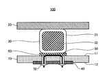
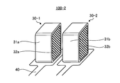
- Sectional drawing of the electrostatic capacitance type touch panel which concerns on Embodiment 1 of this invention The perspective view of the 1st electroconductive member and 2nd electroconductive member which comprise the electrostatic capacitance type touch panel which concerns on Embodiment 2 of this invention.
- Sectional drawing of the capacitive touch panel which concerns on Embodiment 3 of this invention The figure which shows the comparative example with respect to the capacitive touch panel which concerns on Embodiment 3 of this invention.
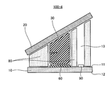
- Sectional drawing of the capacitive touch panel which concerns on Embodiment 4 of this invention Sectional drawing of the capacitive touch panel which concerns on Embodiment 4 of this invention.
- FIG. FIG. 1 is a cross-sectional view of the capacitive touch panel according to Embodiment 1 of the present invention.
- the capacitive touch panel 100 according to the first embodiment includes a substrate 10 having a first substrate surface 11 and a second substrate surface 12, and an operation panel arranged to face the first substrate surface 11. 20 and a plurality of conductive members 30 disposed between the first substrate surface 11 and the operation panel 20.
- the capacitive touch panel 100 includes an electrode pattern 40 disposed on the second substrate surface 12, a jumper wire 50 disposed on the substrate 10 and connecting the electrode pattern 40 and the conductive member 30, and the conductive member 30.
- a conductive adhesive 60 that is disposed between the first substrate surface 11 and includes the jumper wire 50 and connects the conductive member 30 and the jumper wire 50, and solder that connects the jumper wire 50 and the electrode pattern 40. 70.
- FIG. 1 illustrates only one conductive member 30 among the plurality of conductive members 30.
- An example of the conductive member 30 is a gasket.
- the conductive member 30 has a rectangular parallelepiped shape, and includes a non-conductive portion 32 and a conductive portion 31 that covers the side surface of the non-conductive portion 32.
- the side surface is a portion of the outer peripheral surface of the nonconductive portion 32 excluding one end surface of the nonconductive portion 32 on the front side of the paper and the other end surface of the nonconductive portion 32 on the back side of the paper.
- the electrode pattern 40 and the jumper wire 50 are connected by the solder 70, a part of the jumper wire 50 disposed on the first substrate surface 11 side of the substrate 10 is virtual in the entire jumper wire 50. It functions as the electrode pattern 40. That is, the electrode pattern 40 can be moved to the first substrate surface 11 side facing the operation panel 20.
- the electrode pattern 40 By moving the electrode pattern 40 to the first substrate surface 11 side in this way, even when the electrode pattern 40 can be formed only on the second substrate surface 12 side due to manufacturing restrictions of the substrate 10, Compared to the case where the jumper wire 50 is not provided, the distance between the electrode pattern 40 and the conductive member 30 can be reduced, and a decrease in touch detection sensitivity can be suppressed.
- the capacitive touch panel 100 has high touch detection sensitivity when the operation panel 20 and the electrode pattern 40 are connected by a substance having a high dielectric constant. On the other hand, if a substance having a low dielectric constant or an air layer enters between the operation panel 20 and the electrode pattern 40, the touch detection sensitivity is lowered.
- the substrate 10 is a single-sided substrate and the electrode pattern 40 can be disposed only on the second substrate surface 12 on the side opposite to the operation panel 20 side, the substrate 10 is a substance having a low dielectric constant. Lower.
- the capacitive touch panel 100 of the first embodiment even when the electrode pattern 40 can be formed only on the second substrate surface 12 side due to manufacturing restrictions of the substrate 10, the touch detection sensitivity is lowered. Can be suppressed.
- FIG. FIG. 2 is a perspective view of the first conductive member and the second conductive member constituting the capacitive touch panel according to Embodiment 2 of the present invention.
- substrate 10, the operation panel 20, and the jumper wire 50 which are shown in FIG. 1 is abbreviate
- Differences between the capacitive touch panel 100-2 of the second embodiment and the capacitive touch panel 100 of the first embodiment are as follows. (1) In the capacitive touch panel 100-2, the first conductive member 30-1 and the second conductive member 30-2 are used instead of the plurality of conductive members 30.
- the first conductive member 30-1 has a first non-conductive portion 32a and a first conductive portion 31a covering the side surface of the first non-conductive portion 32a.
- the second conductive member 30-2 includes a second non-conductive portion 32b and a second conductive portion 31b that covers the side surface of the second non-conductive portion 32b.
- the end surface of the first non-conductive portion 32a is disposed to face the end surface of the second non-conductive portion 32b.
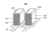
- FIG. 3 is a diagram showing a comparative example for the capacitive touch panel according to Embodiment 2 of the present invention. 3, illustration of the board
- a capacitive touch panel 100A shown in FIG. 3 includes a first conductive member 30-1 having a first nonconductive portion 32a and a first conductive portion 31a covering the side surface of the first nonconductive portion 32a. And a second conductive member 30-2 having a second non-conductive portion 32b and a second conductive portion 31b covering the side surface of the second non-conductive portion 32b.
- the distance between the first conductive member 30-1 and the second conductive member 30-2 becomes narrow.
- the capacitive touch panel 100A shown in FIG. 3 since the outer peripheral surface of the first conductive portion 31a and the outer peripheral surface of the second conductive portion 31b are arranged to face each other, the first conductive portion The part 31a and the second conductive part 31b are capacitively coupled, and the touch detection sensitivity is lowered.
- the first non-conductive portion 32a is arranged.
- the end surface of the first conductive portion 31a covering the side surface of the conductive portion 32a is disposed to face the end surface of the second conductive portion 31b covering the side surface of the second nonconductive portion 32b. Therefore, compared with the capacitive touch panel 100A shown in FIG. 3, in the touch panel 100-2 of the second embodiment, the capacitive coupling between the first conductive portion 31a and the second conductive portion 31b is reduced, and the touch detection sensitivity is reduced. Can be suppressed.
- FIG. FIG. 4 is a cross-sectional view of the capacitive touch panel according to Embodiment 3 of the present invention. 4, illustration of the electrode pattern 40, the jumper wire 50, and the solder 70 shown in FIG. 1 is omitted.
- Differences between the capacitive touch panel 100-3 according to the third embodiment and the capacitive touch panel 100 according to the first embodiment are as follows. (1) The capacitive touch panel 100-3 is provided with a pair of support portions 80. (2) The operation panel 20 is attached to the conductive member 30 at an angle inclined with respect to the extended surface of the substrate 10.
- the pair of support portions 80 are provided in order to prevent horizontal displacement of the operation panel 20.
- Each of the pair of support portions 80 is disposed adjacent to the conductive member 30 and is disposed between the first substrate surface 11 and the operation panel 20.
- FIG. 5 is a diagram showing a comparative example for the capacitive touch panel according to Embodiment 3 of the present invention.
- the capacitive touch panel 100B illustrated in FIG. 5 the pair of support portions 80 illustrated in FIG. 4 is not provided, and the operation panel 20 is attached to the conductive member 30 at an angle inclined with respect to the extended surface of the substrate 10. Installed.
- the conductive member 30 is deformed in the horizontal direction by the pressing force, so that the position in the horizontal direction between the touch part of the operation panel 20 and the electrode pattern 40 (not shown). Displacement is likely to occur.
- the horizontal deformation of the conductive member 30 is suppressed by the support portion 80, and the touch portion of the operation panel 20 and the electrode pattern 40 (not shown) in the horizontal direction are suppressed. Misalignment can be suppressed.
- FIG. FIG. 6 is a cross-sectional view of a capacitive touch panel according to Embodiment 4 of the present invention. 6, illustration of the electrode pattern 40, the jumper wire 50, and the solder 70 shown in FIG. 1 is omitted.
- Differences between the capacitive touch panel 100-4 according to the fourth embodiment and the capacitive touch panel 100-3 according to the third embodiment are as follows. (1) An LED (Light Emitting Diode) 90 that is a light source is provided on the first substrate surface 11 of the substrate 10. (2) The support unit 80 includes the light guide unit 13 that guides the light emitted from the LED 90 to the operation panel 20.
- LED Light Emitting Diode
- Embodiment 4 light emitted from the LED 90 can be guided to an intended position, and light leakage to an unintended portion can be prevented.
- the configuration described in the above embodiment shows an example of the contents of the present invention, and can be combined with another known technique, and can be combined with other configurations without departing from the gist of the present invention. It is also possible to omit or change the part.
Landscapes
- Engineering & Computer Science (AREA)
- General Engineering & Computer Science (AREA)
- Theoretical Computer Science (AREA)
- Human Computer Interaction (AREA)
- Physics & Mathematics (AREA)
- General Physics & Mathematics (AREA)
- Position Input By Displaying (AREA)
- Input From Keyboards Or The Like (AREA)
Abstract
La présente invention concerne un écran tactile à capacité électrostatique 100 pourvu : d'un substrat 10 présentant une première surface de substrat 11 et une seconde surface de substrat 12 ; d'un écran de commande 20 disposé en face de la première surface de substrat 11 ; d'un ou de plusieurs éléments conducteurs 30 disposés entre la première surface de substrat 11 et l'écran de commande 20 ; d'un motif d'électrode 40 disposé sur la seconde surface de substrat 12 ; et d'une ligne de connexion 50, qui est disposée sur le substrat 10, et qui relie ensemble le motif d'électrode 40 et le ou les éléments conducteurs 30. Dans l'écran tactile à capacité électrostatique, la détérioration de la sensibilité de détection peut être supprimée indépendamment de restrictions dans la fabrication de substrats.
Priority Applications (3)
| Application Number | Priority Date | Filing Date | Title |
|---|---|---|---|
| PCT/JP2016/056310 WO2017149680A1 (fr) | 2016-03-01 | 2016-03-01 | Écran tactile à capacité électrostatique |
| JP2018502927A JP6522229B2 (ja) | 2016-03-01 | 2016-03-01 | 静電容量式タッチパネル |
| CN201680079113.2A CN108700950B (zh) | 2016-03-01 | 2016-03-01 | 静电电容式触摸面板 |
Applications Claiming Priority (1)
| Application Number | Priority Date | Filing Date | Title |
|---|---|---|---|
| PCT/JP2016/056310 WO2017149680A1 (fr) | 2016-03-01 | 2016-03-01 | Écran tactile à capacité électrostatique |
Publications (1)
| Publication Number | Publication Date |
|---|---|
| WO2017149680A1 true WO2017149680A1 (fr) | 2017-09-08 |
Family
ID=59743597
Family Applications (1)
| Application Number | Title | Priority Date | Filing Date |
|---|---|---|---|
| PCT/JP2016/056310 Ceased WO2017149680A1 (fr) | 2016-03-01 | 2016-03-01 | Écran tactile à capacité électrostatique |
Country Status (3)
| Country | Link |
|---|---|
| JP (1) | JP6522229B2 (fr) |
| CN (1) | CN108700950B (fr) |
| WO (1) | WO2017149680A1 (fr) |
Families Citing this family (1)
| Publication number | Priority date | Publication date | Assignee | Title |
|---|---|---|---|---|
| KR102398927B1 (ko) * | 2021-10-05 | 2022-05-17 | 이두환 | 터치 스위치용 전도성 폼 개스킷 |
Citations (4)
| Publication number | Priority date | Publication date | Assignee | Title |
|---|---|---|---|---|
| JP2007035334A (ja) * | 2005-07-25 | 2007-02-08 | Calsonic Kansei Corp | 静電容量式タッチスイッチ |
| JP2009187818A (ja) * | 2008-02-07 | 2009-08-20 | Jst Mfg Co Ltd | コンタクト |
| JP2014527271A (ja) * | 2012-05-25 | 2014-10-09 | シルリュック産業株式会社 | 静電容量感知型タッチスイッチ |
| JP2016009586A (ja) * | 2014-06-24 | 2016-01-18 | 三菱電機株式会社 | 冷蔵庫 |
Family Cites Families (8)
| Publication number | Priority date | Publication date | Assignee | Title |
|---|---|---|---|---|
| JP2010244772A (ja) * | 2009-04-03 | 2010-10-28 | Sony Corp | 静電容量式タッチ部材及びその製造方法、並びに静電容量式タッチ検出装置 |
| US8416214B2 (en) * | 2010-03-24 | 2013-04-09 | Whirlpool Corporation | Touch screen coupling having tactile response capability |
| CN104350450B (zh) * | 2012-05-31 | 2018-01-26 | 大日本印刷株式会社 | 静电电容式触摸面板基板和显示装置 |
| WO2013187397A1 (fr) * | 2012-06-12 | 2013-12-19 | 株式会社フジクラ | Dispositif d'entrée |
| US20140069795A1 (en) * | 2012-09-11 | 2014-03-13 | City University Of Hong Kong | Sensing arrangement, sensor and apparatus comprising same, and method of manufacture thereof |
| DE102014217439A1 (de) * | 2013-09-02 | 2015-03-05 | Honda Motor Co., Ltd. | Schaltersystem |
| CN104571667B (zh) * | 2013-10-26 | 2018-05-29 | 宝宸(厦门)光学科技有限公司 | 触控面板及其制造方法 |
| CN203706185U (zh) * | 2014-01-08 | 2014-07-09 | 北京京东方光电科技有限公司 | 触摸屏和显示装置 |
-
2016
- 2016-03-01 WO PCT/JP2016/056310 patent/WO2017149680A1/fr not_active Ceased
- 2016-03-01 JP JP2018502927A patent/JP6522229B2/ja not_active Expired - Fee Related
- 2016-03-01 CN CN201680079113.2A patent/CN108700950B/zh not_active Expired - Fee Related
Patent Citations (4)
| Publication number | Priority date | Publication date | Assignee | Title |
|---|---|---|---|---|
| JP2007035334A (ja) * | 2005-07-25 | 2007-02-08 | Calsonic Kansei Corp | 静電容量式タッチスイッチ |
| JP2009187818A (ja) * | 2008-02-07 | 2009-08-20 | Jst Mfg Co Ltd | コンタクト |
| JP2014527271A (ja) * | 2012-05-25 | 2014-10-09 | シルリュック産業株式会社 | 静電容量感知型タッチスイッチ |
| JP2016009586A (ja) * | 2014-06-24 | 2016-01-18 | 三菱電機株式会社 | 冷蔵庫 |
Also Published As
| Publication number | Publication date |
|---|---|
| JP6522229B2 (ja) | 2019-05-29 |
| JPWO2017149680A1 (ja) | 2018-07-05 |
| CN108700950B (zh) | 2021-03-12 |
| CN108700950A (zh) | 2018-10-23 |
Similar Documents
| Publication | Publication Date | Title |
|---|---|---|
| KR102575557B1 (ko) | 표시장치 및 연성회로기판 | |
| KR102632292B1 (ko) | 터치 패널 | |
| KR101247915B1 (ko) | 투광형 입력 장치와 그의 제조 방법 | |
| US8199127B2 (en) | Display panel | |
| US9690439B2 (en) | Touch panel | |
| CN109388288A (zh) | 一种显示面板及显示装置 | |
| CN104793777A (zh) | 触控面板与触控显示装置 | |
| TW201519022A (zh) | 觸控面板 | |
| CN103902110A (zh) | 触控面板 | |
| WO2016027555A1 (fr) | Panneau tactile à capacité électrostatique | |
| US10761668B2 (en) | Touch substrate, touch panel, and touch display device | |
| CN107749239A (zh) | 显示面板、显示装置及显示面板的制作方法 | |
| JP2012043298A (ja) | 入力装置及びその製造方法 | |
| US9244571B2 (en) | Touch sensing device | |
| US20140152915A1 (en) | Touch panel | |
| KR101506275B1 (ko) | 벤딩 라인이 형성된 터치 스크린 패널용 연성 인쇄 회로 기판 | |
| TWI590137B (zh) | 觸控面板及應用其之觸控顯示裝置 | |
| US10156939B2 (en) | Light source assembly of optical touch device | |
| US8780067B1 (en) | Bridging structure for signal transmission of touch panel | |
| JP6522229B2 (ja) | 静電容量式タッチパネル | |
| JP6147469B2 (ja) | タッチセンサ | |
| JP2007013050A (ja) | 反射型フォトセンサ | |
| KR102281769B1 (ko) | 터치입력장치 | |
| JP2019191791A (ja) | タッチパネル装置 | |
| US20140192010A1 (en) | Capacitive Touch Panel |
Legal Events
| Date | Code | Title | Description |
|---|---|---|---|
| ENP | Entry into the national phase |
Ref document number: 2018502927 Country of ref document: JP Kind code of ref document: A |
|
| NENP | Non-entry into the national phase |
Ref country code: DE |
|
| 121 | Ep: the epo has been informed by wipo that ep was designated in this application |
Ref document number: 16892524 Country of ref document: EP Kind code of ref document: A1 |
|
| 122 | Ep: pct application non-entry in european phase |
Ref document number: 16892524 Country of ref document: EP Kind code of ref document: A1 |