WO2017149767A1 - Dispositif de recuit laser, masque, transistor à couches minces et procédé de recuit laser - Google Patents
Dispositif de recuit laser, masque, transistor à couches minces et procédé de recuit laser Download PDFInfo
- Publication number
- WO2017149767A1 WO2017149767A1 PCT/JP2016/056822 JP2016056822W WO2017149767A1 WO 2017149767 A1 WO2017149767 A1 WO 2017149767A1 JP 2016056822 W JP2016056822 W JP 2016056822W WO 2017149767 A1 WO2017149767 A1 WO 2017149767A1
- Authority
- WO
- WIPO (PCT)
- Prior art keywords
- openings
- opening region
- laser annealing
- opening
- substrate
- Prior art date
- Legal status (The legal status is an assumption and is not a legal conclusion. Google has not performed a legal analysis and makes no representation as to the accuracy of the status listed.)
- Ceased
Links
Images







Classifications
-
- H—ELECTRICITY
- H10—SEMICONDUCTOR DEVICES; ELECTRIC SOLID-STATE DEVICES NOT OTHERWISE PROVIDED FOR
- H10P—GENERIC PROCESSES OR APPARATUS FOR THE MANUFACTURE OR TREATMENT OF DEVICES COVERED BY CLASS H10
- H10P34/00—Irradiation with electromagnetic or particle radiation of wafers, substrates or parts of devices
- H10P34/40—Irradiation with electromagnetic or particle radiation of wafers, substrates or parts of devices with high-energy radiation
- H10P34/42—Irradiation with electromagnetic or particle radiation of wafers, substrates or parts of devices with high-energy radiation with electromagnetic radiation, e.g. laser annealing
-
- H—ELECTRICITY
- H10—SEMICONDUCTOR DEVICES; ELECTRIC SOLID-STATE DEVICES NOT OTHERWISE PROVIDED FOR
- H10P—GENERIC PROCESSES OR APPARATUS FOR THE MANUFACTURE OR TREATMENT OF DEVICES COVERED BY CLASS H10
- H10P14/00—Formation of materials, e.g. in the shape of layers or pillars
- H10P14/20—Formation of materials, e.g. in the shape of layers or pillars of semiconductor materials
- H10P14/38—Formation of materials, e.g. in the shape of layers or pillars of semiconductor materials characterised by treatments done after the formation of the materials
- H10P14/3802—Crystallisation or recrystallisation of non-monocrystalline semiconductor materials, e.g. regrowth
- H10P14/3808—Crystallisation or recrystallisation of non-monocrystalline semiconductor materials, e.g. regrowth using laser beams
- H10P14/381—Beam shaping, e.g. using a mask
- H10P14/3812—Shape of mask
-
- H—ELECTRICITY
- H10—SEMICONDUCTOR DEVICES; ELECTRIC SOLID-STATE DEVICES NOT OTHERWISE PROVIDED FOR
- H10P—GENERIC PROCESSES OR APPARATUS FOR THE MANUFACTURE OR TREATMENT OF DEVICES COVERED BY CLASS H10
- H10P14/00—Formation of materials, e.g. in the shape of layers or pillars
- H10P14/20—Formation of materials, e.g. in the shape of layers or pillars of semiconductor materials
- H10P14/38—Formation of materials, e.g. in the shape of layers or pillars of semiconductor materials characterised by treatments done after the formation of the materials
- H10P14/3802—Crystallisation or recrystallisation of non-monocrystalline semiconductor materials, e.g. regrowth
- H10P14/3808—Crystallisation or recrystallisation of non-monocrystalline semiconductor materials, e.g. regrowth using laser beams
- H10P14/381—Beam shaping, e.g. using a mask
-
- H—ELECTRICITY
- H10—SEMICONDUCTOR DEVICES; ELECTRIC SOLID-STATE DEVICES NOT OTHERWISE PROVIDED FOR
- H10P—GENERIC PROCESSES OR APPARATUS FOR THE MANUFACTURE OR TREATMENT OF DEVICES COVERED BY CLASS H10
- H10P14/00—Formation of materials, e.g. in the shape of layers or pillars
- H10P14/20—Formation of materials, e.g. in the shape of layers or pillars of semiconductor materials
- H10P14/38—Formation of materials, e.g. in the shape of layers or pillars of semiconductor materials characterised by treatments done after the formation of the materials
- H10P14/3802—Crystallisation or recrystallisation of non-monocrystalline semiconductor materials, e.g. regrowth
- H10P14/382—Scanning of a beam
-
- H—ELECTRICITY
- H10—SEMICONDUCTOR DEVICES; ELECTRIC SOLID-STATE DEVICES NOT OTHERWISE PROVIDED FOR
- H10P—GENERIC PROCESSES OR APPARATUS FOR THE MANUFACTURE OR TREATMENT OF DEVICES COVERED BY CLASS H10
- H10P95/00—Generic processes or apparatus for manufacture or treatments not covered by the other groups of this subclass
- H10P95/90—Thermal treatments, e.g. annealing or sintering
-
- B—PERFORMING OPERATIONS; TRANSPORTING
- B23—MACHINE TOOLS; METAL-WORKING NOT OTHERWISE PROVIDED FOR
- B23K—SOLDERING OR UNSOLDERING; WELDING; CLADDING OR PLATING BY SOLDERING OR WELDING; CUTTING BY APPLYING HEAT LOCALLY, e.g. FLAME CUTTING; WORKING BY LASER BEAM
- B23K26/00—Working by laser beam, e.g. welding, cutting or boring
- B23K26/02—Positioning or observing the workpiece, e.g. with respect to the point of impact; Aligning, aiming or focusing the laser beam
- B23K26/06—Shaping the laser beam, e.g. by masks or multi-focusing
- B23K26/064—Shaping the laser beam, e.g. by masks or multi-focusing by means of optical elements, e.g. lenses, mirrors or prisms
- B23K26/066—Shaping the laser beam, e.g. by masks or multi-focusing by means of optical elements, e.g. lenses, mirrors or prisms by using masks
-
- H—ELECTRICITY
- H10—SEMICONDUCTOR DEVICES; ELECTRIC SOLID-STATE DEVICES NOT OTHERWISE PROVIDED FOR
- H10P—GENERIC PROCESSES OR APPARATUS FOR THE MANUFACTURE OR TREATMENT OF DEVICES COVERED BY CLASS H10
- H10P14/00—Formation of materials, e.g. in the shape of layers or pillars
- H10P14/20—Formation of materials, e.g. in the shape of layers or pillars of semiconductor materials
- H10P14/34—Deposited materials, e.g. layers
- H10P14/3402—Deposited materials, e.g. layers characterised by the chemical composition
- H10P14/3404—Deposited materials, e.g. layers characterised by the chemical composition being Group IVA materials
- H10P14/3411—Silicon, silicon germanium or germanium
Definitions
- the present invention provides a laser annealing apparatus for irradiating a substrate with laser light through an opening formed in a mask, a mask constituting the laser annealing apparatus, a thin film transistor laser annealed by the laser annealing apparatus, and the laser annealing apparatus.
- the present invention relates to a laser annealing method to be used.
- a TFT (Thin Film Transistor) type liquid crystal display is obtained by bonding a TFT substrate and a color filter substrate having R (red), G (green), and B (blue) colors with a necessary gap therebetween.
- An image can be displayed by injecting liquid crystal between the substrate and the color filter substrate and controlling the light transmittance of the liquid crystal molecules for each pixel.
- data lines and scanning lines are arranged in a grid pattern in the vertical and horizontal directions, and pixels composed of TFTs are formed at locations where the data lines and the scanning lines intersect.
- a drive circuit configured by TFTs and driving data lines and scanning lines is formed around a display region including a plurality of pixels.
- amorphous silicon (amorphous, a-Si) TFTs using silicon semiconductors, low-temperature polysilicon TFTs in which the semiconductor layer is polysilicon (polycrystalline, p-Si), etc. are being developed. Yes.
- the a-Si TFT has a high resistance and a small leakage current (leakage current).
- the p-Si TFT has a significantly higher electron mobility than the a-Si TFT.
- a polysilicon layer can be formed by annealing the amorphous silicon layer by irradiating it with laser light.
- a laser annealing apparatus that forms laser light emitted from a laser light source into a parallel beam by a lens group, and irradiates the shaped parallel beam onto a substrate via a light shielding member having an opening and a microlens array.
- a predetermined number of openings are arranged in the light-shielding member along the scanning direction of the substrate, and each cycle of the substrate is moved by the pitch of the openings, thereby irradiating laser light for one cycle. Since the laser beam is irradiated to the required part of the substrate by the number of times equal to the number of openings in the scan, the same amount of laser beam can be irradiated (see Patent Document 1).
- the conventional laser annealing apparatus irradiates a required portion of the substrate with the same amount of laser light in one cycle of scanning. For this reason, for example, when the gap portion between the source electrode and the drain electrode and the portion immediately below the part of the source electrode and the drain electrode are the required portions, the polysilicon layer of each of the gap portion and the portion immediately below the electrode The electron mobility is similarly increased, and the leakage current of the TFT is increased.
- the present invention has been made in view of such circumstances, and a laser annealing apparatus capable of performing an annealing process partially different in electron mobility, a mask constituting the laser annealing apparatus, and laser annealing using the laser annealing apparatus.
- Another object of the present invention is to provide a laser annealing method using the thin film transistor and the laser annealing apparatus.
- a laser annealing apparatus is a laser annealing apparatus that includes a mask having a plurality of openings formed along a scanning direction, and irradiates a substrate with laser light through the openings.
- the plurality of openings have first opening regions that are aligned along the scanning direction and have the same shape, and some of the openings are in a predetermined direction with respect to the first opening region. It has the 2nd opening area
- the mask according to the embodiment of the present invention is a mask in which a plurality of openings are formed along the scanning direction of the substrate, and the plurality of openings are aligned along the scanning direction and have the same shape. It has a 1st opening area
- a thin film transistor includes a gate electrode formed on a surface of a substrate, an amorphous semiconductor film formed above the gate electrode, and the amorphous semiconductor film.
- the source electrode, the drain electrode formed on the amorphous semiconductor film, and the amorphous semiconductor film directly below a part of each of the source electrode and the drain electrode among the amorphous semiconductor films are described above.
- the crystalline semiconductor film formed by annealing with the laser annealing apparatus according to the embodiment, and the amorphous semiconductor film between the source electrode and the drain electrode among the amorphous semiconductor film is formed as described above.
- the laser annealing method according to the embodiment of the present invention is a laser annealing method using the laser annealing apparatus according to the above-described embodiment, and is formed on the mask by moving the relative position of the substrate and the mask along the scanning direction.
- the substrate is irradiated with laser light through the plurality of openings.
- FIG. 1 is a schematic diagram showing an example of the configuration of the laser annealing apparatus 100 of the present embodiment.
- a laser annealing apparatus 100 includes a laser light source 50 that emits laser light, an optical system 40 that includes a lens group for shaping the laser light emitted from the laser light source 50 into a parallel beam, an opening described below, and A mask (light shielding plate) 30 having a mask portion 31 in which microlenses are arranged in an array is provided.
- the parallel beam formed by the optical system 40 is partially irradiated to a required portion of the substrate 10 through the opening provided in the mask portion 31 and the microlens.
- the substrate 10 is transported at a constant speed by a drive mechanism (not shown).
- the laser light source 50 irradiates laser light at time intervals at which the irradiation position of the substrate 10 reaches a position corresponding to the opening.
- the laser annealing apparatus 100 may have a configuration in which the substrate 10 is fixed and the mask 30 is moved instead of the configuration in which the substrate 10 is moved. Below, the example which moves the board
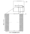
- FIG. 2 is a schematic plan view showing an example of the configuration of the mask 30 of the present embodiment.
- a rectangular mask portion 31 is formed on the mask 30.
- the dimension of the mask portion 31 in the scanning direction (vertical direction) is W, and the dimension in the direction orthogonal to the scanning direction (horizontal direction) is L.
- the mask unit 31 is provided with microlenses 21 in an array at equal intervals in the scanning direction and in the direction orthogonal to the scanning direction.
- An opening which will be described later, is formed at the center position of each microlens 21 in plan view.
- the vertical dimension W of the mask portion 31 can be, for example, about 5 mm, and the horizontal dimension L can be about 37 mm, but each dimension is not limited to these numerical values.
- Twenty macro lenses 21 are arranged at equal intervals in the scanning direction (vertical direction). Since one aperture corresponds to one macro lens 21, the mask 30 has 20 apertures formed at equal intervals in the scanning direction (vertical direction).
- FIG. 3 is a schematic diagram showing the positional relationship between the opening 32 and the microlens 21 of the present embodiment.
- FIG. 3 shows the positional relationship between the opening 32 and the microlens 21 in a front view, and shows the position of the opening 32 in a plan view on the basis of the position of the microlens 21 corresponding to the opening 32.
- the size of the opening 32 and the size of the irradiation pattern are described equivalently.
- the size of the part 32 is larger than the size of the irradiation pattern.
- the mask portion 31 has a plurality of openings 32 and microlenses (lenses) 21.
- the microlens 21 is formed on the transparent substrate 20 corresponding to the opening 32, and the transparent substrate 20 and the mask 30 are integrated.
- a rectangular opening 32 is arranged at the center of the microlens 21 that is circular in plan view.
- the mask 30 and the incident surface of the microlens 21 are spaced apart by an appropriate length.
- the maximum size (circular diameter in plan view) of the microlens 21 can be, for example, about 150 ⁇ m to 400 ⁇ m, but is not limited to these numerical values.
- the plurality of formed microlenses 21 is also referred to as a microlens array.
- the laser light that has passed through the opening 32 is condensed by the microlens 21, and the condensed laser light is A required portion on the substrate 10 is partially irradiated corresponding to each of the plurality of openings 32 (that is, the microlens 21).
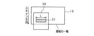
- FIG. 4A shows a state in which the mask 30 is set at a predetermined position, and shows a state before the movement of the substrate 10 in the scanning direction is started. From the state shown in FIG. 4A, the substrate 10 is moved in the scanning direction at a constant speed.
- the laser light source 50 irradiates laser light at time intervals at which the irradiation position of the substrate 10 reaches a position corresponding to the opening 32. For example, in the case of the opening 32 illustrated in FIG. 2, the same portion of the substrate 10 is irradiated with the laser light 20 times.
- FIG. 4A shows a state in which the mask 30 is set at a predetermined position, and shows a state before the movement of the substrate 10 in the scanning direction is started. From the state shown in FIG. 4A, the substrate 10 is moved in the scanning direction at a constant speed.
- the laser light source 50 irradiates laser light at time intervals at which the irradiation position of the substrate 10 reaches a position corresponding to the opening 32
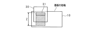
- FIG. 4B shows a state in which the substrate 10 is moved at a constant speed and moved to the final position in the scanning direction (by the distance Z).
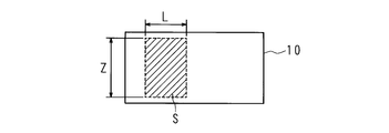
- the substrate 10 By moving the substrate 10 to the state shown in FIG. 4B, it is possible to partially irradiate a laser beam to a required portion within the irradiation region S of the substrate 10 as shown in FIG. 4C.
- the mask 30 In the state shown in FIG. 4C, the mask 30 is moved by a distance L in the direction orthogonal to the scanning direction, and the substrate 10 is moved in the scanning direction in the same manner as shown in FIGS. 4A and 4B, thereby increasing the irradiation region S. be able to.
- the size of the substrate 10 and the size of the mask 30 are shown to be approximately the same, but the size of the substrate 10 is actually much larger than that in FIG. 4.
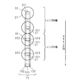
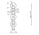
- FIG. 5 is a schematic diagram showing a first example of the opening 32 of the mask 30 of the present embodiment. In the following, both are shown so that the positional relationship between the opening 32 and the microlens 21 can be understood, and for convenience, only one row along the scanning direction is shown.
- (M + N) openings 32 are arranged at predetermined intervals in the scanning direction. All (M + N) openings 32 have first opening regions 321 that are aligned at equal intervals along the scanning direction and have the same shape.
- the center of the position of the first opening area 321 corresponds to the center of the microlens 21, and the shape of the first opening area 321 is rectangular.
- N openings 32 have a second opening region 322 connected to the first opening region 321 in a predetermined direction with respect to the first opening region 321.
- the predetermined direction is a direction orthogonal to the scan direction.
- the predetermined direction is not limited to this, and may be a scanning direction.
- the N openings 32 are connected to a pair of second opening regions 322 and 322 in a direction orthogonal to the scanning direction with the first opening region 321 interposed therebetween.
- the same portion of the substrate 10 is scanned with (N + M) times of laser light through the opening 32 having the first opening region 321 in one cycle of scanning, and the first opening region 321 and Laser light is irradiated N times through the opening having both of the second opening regions 322.
- the number of the plurality of openings 32 is (N + M), and the number of some of the openings 32 is N.
- the substrate 10 is moved at a constant speed along the scanning direction.
- the laser light source 50 irradiates laser light at time intervals at which the irradiation position of the substrate 10 reaches a position corresponding to the opening 32.
- the same portion of the substrate 10 is irradiated with (N + M) times of laser light in one cycle of scanning.
- a required portion of the substrate 10 corresponding to the first opening region 321 includes 1
- the laser beam is irradiated (N + M) times in the cycle scan.
- a required portion of the substrate 10 corresponding to the second opening region 322 is irradiated with N times of laser light in one cycle scan.
- the portion 151 corresponding to the first opening region 321 of the substrate 10 can increase the amount of laser light irradiation and increase the electron mobility, and is located at a position in a predetermined direction with respect to the first opening region 321.
- the portion 152 corresponding to the second opening region 322 connected to the opening region 321 can reduce the irradiation amount of the laser light and prevent the electron mobility from increasing too much. As a result, annealing treatment with partially different electron mobility can be performed in one cycle scan, and crystalline semiconductor films with different electron mobility can be formed.
- a part of the plurality of openings 32 includes a pair of second opening regions 322 that are connected to the first opening region 321 with the first opening region 321 interposed therebetween in a predetermined direction with respect to the first opening region 321.
- a pair of second opening regions 322 and 323 are arranged in a predetermined direction with the first opening region 321 interposed therebetween.
- a crystalline semiconductor film arranged in a predetermined direction in the order of a region 152 having a relatively high electron mobility, a region 151 having a large electron mobility, and a region 152 having a relatively large electron mobility is formed in one cycle of scanning. Can do.
- the size of the opening 32 (the first opening region 321 and the second opening region 322, 323) and the irradiation pattern (the first opening region 321 and the second opening region 322 of the substrate 10).
- the size of the opening 32 is larger than the size of the irradiation pattern because the laser light is actually condensed by the microlens 21. Is also big. The same applies to FIG. 6 and subsequent figures.
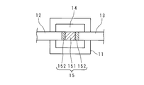
- FIG. 6 is a schematic view showing the main part of a thin film transistor annealed by the laser annealing apparatus 100 of this embodiment
- FIG. 7 is a side view of the thin film transistor annealed by the laser annealing apparatus 100 of this embodiment. It is a schematic diagram which shows the principal part. 6 and 7, only the main part is shown for simplicity.
- the thin film transistor annealed by the laser annealing apparatus 100 of the present embodiment includes the gate electrode 11 formed on the surface of the substrate 10, and the gate electrode 11.
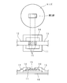
- FIG. 8 is a schematic diagram showing a main part of an ideal thin film transistor annealed by a conventional laser annealing apparatus.
- the upper part of FIG. 8 shows openings provided corresponding to the lenses, and the shapes of the openings are all the same.
- 8 shows the main part of the thin film transistor in plan view
- the lower part of FIG. 8 shows the main part of the thin film transistor in side view.
- a portion of the substrate corresponding to the opening corresponds to a gap between the source electrode 12 and the drain electrode 13.
- a gap between the source electrode 12 and the drain electrode 13 is formed by the crystalline semiconductor film 15, and is directly below the source electrode 12 and the drain electrode 13. Is formed of an amorphous semiconductor film 14. With this configuration, the leakage current can be reduced and the drive current can be increased.
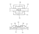
- FIG. 9 is a schematic view showing a main part of an example of a conventional thin film transistor.
- the shapes of the openings formed in the mask are all the same.
- a portion of the substrate corresponding to the opening is a gap between the source electrode 12 and the drain electrode 13.
- the region irradiated with the laser light may deviate from the gap part due to a positional deviation when the substrate 10 is transported in the scanning direction or a deviation of the optical axis of the laser light.
- a part of the amorphous semiconductor film 14 is formed.
- the electron mobility in a part of the gap portion becomes small, and the driving current cannot be increased.
- FIG. 10 is a schematic diagram showing the main part of another example of a thin film transistor annealed by a conventional laser annealing apparatus.
- the opening shown in FIG. 10 has a lateral dimension so that a part of the source electrode 12 and the part of the drain electrode 13 are also irradiated with laser light. Is slightly longer.
- the gap between the source electrode 12 and the drain electrode 13 is always in the crystalline semiconductor film 15. Formed with.
- a region immediately below a part of each of the source electrode 12 and the drain electrode 13 is also formed of the crystalline semiconductor film 15, so that there is a disadvantage that leakage current increases.
- the portion 151 corresponding to the first opening region 321 of the substrate 10 can increase the amount of laser light irradiation and increase the electron mobility, and the first opening region 321.
- the portion 152 corresponding to the second opening region 322 connected to the first opening region 321 at a position in a predetermined direction can reduce the irradiation amount of the laser light and prevent the electron mobility from increasing too much. .
- annealing treatment with partially different electron mobility can be performed in one cycle scan, and crystalline semiconductor films with different electron mobility can be formed.
- the gap between the source electrode 12 and the drain electrode 13 is formed of a crystalline semiconductor film 15 having a high electron mobility. Since the crystalline semiconductor film 15 having a relatively high electron mobility is formed immediately below a part of each of the drain electrode 13 and the drain electrode 13, a leakage current can be reduced and a driving current can be increased.
- FIG. 11 is a schematic diagram showing a second example of the opening 32 of the mask 30 of the present embodiment.
- the difference from the first embodiment shown in FIG. 5 is that, in the second embodiment, the opening 32 having only the first opening region 321 and the opening having both the first opening region 321 and the second opening region 322. 32 are alternately arranged along the scanning direction. By arranging them alternately, variations such as unevenness in incident light and shift in transport of the substrate 10 are diffused (averaged), and a thin film transistor having uniform characteristics can be manufactured.
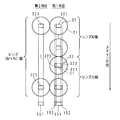
- FIG. 12 is a schematic diagram showing a third example of the opening 32 of the mask 30 of the present embodiment.
- the type of the opening 32 differs depending on the row of the openings 32 arranged in the scanning direction.
- the first row is constituted by the same row of openings 32 as in the first embodiment, and in the second row, all (M + N) openings 32 have only the first opening region 321.
- crystalline semiconductor films having different modes of electron mobility can be formed in one cycle of scanning.
- FIG. 13 is a schematic diagram showing a fourth example of the opening 32 of the mask 30 of the present embodiment.
- all (M + N) openings 32 have first opening regions 321 that are aligned at equal intervals along the scanning direction and have the same shape.
- the center of the position of the first opening area 321 corresponds to the center of the microlens 21, and the shape of the first opening area 321 is rectangular.
- N openings 32 have a second opening region 323 connected to the first opening region 321 in a predetermined direction with respect to the first opening region 321.
- the predetermined direction is a direction orthogonal to the scan direction.
- K openings 32 have a second opening region 322 at a position facing the second opening region 323 across the first opening region 321.
- the substrate portion 151 corresponding to the first opening region 321 is irradiated with (M + N) times of laser light
- the substrate portion 152 corresponding to the second opening region 323 is irradiated with N times of laser light.
- the substrate portion 153 corresponding to the second opening region 322 is irradiated with K times of laser light.
- FIG. 14 is a schematic diagram showing a fifth example of the opening 32 of the mask 30 of the present embodiment.
- all (M + N) openings 32 have first opening regions 321 that are aligned at equal intervals along the scanning direction and have the same shape.
- the center of the position of the first opening area 321 corresponds to the center of the microlens 21, and the shape of the first opening area 321 is rectangular.
- M openings 32 have a second opening region 322 connected to the first opening region 321 in a predetermined direction with respect to the first opening region 321.
- the predetermined direction is a direction orthogonal to the scan direction.
- the second opening region 322 is provided on the left side of the first opening region 321.
- N openings 32 have second opening regions 323 connected to the first opening regions 321 in a predetermined direction with respect to the first opening regions 321.
- the second opening region 323 is provided on the right side of the first opening region 321.
- the shape and size of each of the (M + N) openings 32 are the same, and the positions of the M openings 32 are shifted to the left from the center. Further, the positions of the N openings 32 are shifted from the center to the right side.
- the substrate portion 151 corresponding to the first opening region 321 is irradiated with (M + N) times of laser light
- the substrate portion 152 corresponding to the second opening region 322 is irradiated with M times of laser light.
- the substrate portion 152 corresponding to the second opening region 323 is irradiated with laser light N times. Accordingly, crystalline semiconductor films having different electron mobilities can be formed in one cycle of scanning.
- the predetermined direction is a direction orthogonal to the scanning direction
- the first opening region 321 and the second opening regions 322 and 323 have the same dimensions in the scanning direction.
- the crystalline semiconductor film having the same dimension in the scanning direction and the electron mobility being relatively large, large, and relatively large and arranged along the direction orthogonal to the scanning direction is formed. Can do.
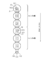
- FIG. 15 is a schematic view showing a sixth example of the opening 32 of the mask 30 of the present embodiment.
- all (M + N) openings 32 have first opening regions 321 that are aligned at equal intervals along the scanning direction and have the same shape.
- the center of the position of the first opening area 321 corresponds to the center of the microlens 21, and the shape of the first opening area 321 is rectangular.
- N openings 32 are a set of second openings that are connected to the first opening area 321 with the first opening area 321 in the scanning direction with respect to the first opening area 321. Open regions 324 and 325 are provided. In other words, the N openings 32 have a pair of second opening regions 324 and 325 in the scanning direction with the first opening region 321 interposed therebetween.
- the portion 151 corresponding to the first opening region 321 of the substrate 10 can increase the amount of laser light irradiation and increase the electron mobility.
- the portion 152 corresponding to the second opening regions 324 and 325 It is possible to prevent the irradiation amount from decreasing and the electron mobility from increasing too much. As a result, annealing treatment with partially different electron mobility can be performed in one cycle scan, and crystalline semiconductor films with different electron mobility can be formed.
- FIG. 16 is a schematic diagram showing a seventh example of the opening 32 of the mask 30 of the present embodiment.
- all (M + N) openings 32 have first opening regions 321 that are aligned at equal intervals along the scanning direction and have the same shape.
- the center of the position of the first opening area 321 corresponds to the center of the microlens 21, and the shape of the first opening area 321 is rectangular.
- the M openings 32 have a second opening region 324 connected to the first opening region 321 in the scanning direction with respect to the first opening region 321.
- the second opening region 324 is provided above the first opening region 321.
- N openings 32 have a second opening region 325 connected to the first opening region 321 in the scanning direction with respect to the first opening region 321.
- a second opening region 325 is provided below the first opening region 321.
- the shape and size of each of the (M + N) openings 32 are the same, and the positions of the M openings 32 are shifted upward from the center (backward in the scanning direction). Further, the positions of the N openings 32 are shifted from the center to the lower side (forward in the scanning direction).
- the substrate portion 151 corresponding to the first opening region 321 is irradiated with (M + N) times of laser light
- the substrate portion 152 corresponding to the second opening region 324 is irradiated with M times of laser light.
- the portion 152 of the substrate corresponding to the second opening region 325 is irradiated with laser light N times. Accordingly, crystalline semiconductor films having different electron mobilities can be formed in one cycle of scanning.
- the predetermined direction is the scanning direction
- the dimensions of the first opening region 321 and the second opening regions 324 and 325 in the direction orthogonal to the scanning direction are the same. is there.
- a crystalline semiconductor film is formed in which the dimensions in the direction orthogonal to the scanning direction are the same and the electron mobility is relatively large, large, and relatively large, arranged in the order of the scanning direction. Can do.
- the first opening region 321 has a rectangular shape. Since the first opening region 321 has a rectangular shape, a portion of the substrate corresponding to the first opening region 321 can be a gap portion between the source electrode 12 and the drain electrode 13. Further, the second opening regions 322, 323, 324, and 325 connected to the first opening region 321 can be portions directly below the electrodes of the source electrode 12 and the drain electrode 13.
- the laser annealing apparatus 100 of the present embodiment includes the microlens 21 that condenses the laser light, it is possible to partially irradiate the laser beam to a required portion of the substrate and perform partial laser annealing. Moreover, since the laser annealing apparatus 100 of this Embodiment is provided with the laser light source 50, it can perform partial laser annealing.
- FIG. 17 is a schematic diagram showing an eighth example of the opening 32 of the mask 30 of the present embodiment.
- the opening 32 is provided with minute rectangular adjustment members 35 arranged in a lattice pattern.
- the adjusting member 35 is for adjusting the amount of laser beam irradiation, and any suitable material can be used as long as it is made of a material that reduces the amount of laser beam transmission.
- the pattern B the position of the adjustment member 35 of the pattern A is opened, and the adjustment member 35 is provided at the position where the pattern A is opened.
- the positions of the adjustment members 35 complement each other, so that the unevenness of the amount of laser light irradiation can be made uniform.
- the electron mobility of the crystalline semiconductor layer can be adjusted to a required value by adjusting the amount of laser light applied to a required portion of the substrate 10 in one cycle of scanning.
- FIG. 18 is a schematic diagram showing a ninth example of the opening 32 of the mask 30 of the present embodiment.
- the opening 32 is provided with a minute rectangular adjustment member 36 arranged in a slit shape.
- the position of the adjustment member 36 of the pattern C is opened, and the adjustment member 36 is provided in the opening position of the pattern C.
- the position of the adjusting member 36 that adjusts the laser beam irradiation amount is set to a complementary position so that the laser beam irradiation amount can be made uniform and uniform.
- the electron mobility of the crystalline semiconductor layer can be adjusted to a required value by adjusting the amount of laser light applied to a required portion of the substrate 10 in one cycle of scanning.
- the opening 32 as shown in FIGS. 17 and 18 may be applied to the opening 32 having only the first opening region 321, or the first opening region 321 and the second opening regions 322, 323, 324, 325. It can also be applied to the opening 32 having both of the above. 17 and 18 may be applied to both the first opening region 321 and the second opening regions 322, 323, 324, and 325, or the first opening region 321 and the second opening region 321 You may apply only to either one of 2 opening area
- FIG. 19 is a flowchart showing an example of a laser annealing method using the laser annealing apparatus 100 of the present embodiment.
- the laser annealing apparatus 100 is referred to as an apparatus 100 for the sake of simplicity.
- the apparatus 100 sets the mask 30 at a predetermined position (S11), and irradiates laser light (S12).
- the apparatus 100 moves the substrate 10 in the scanning direction at a constant speed (S13).
- the laser light source 50 irradiates laser light at time intervals at which the irradiation position of the substrate 10 reaches a position corresponding to the opening 32 of the mask 30.
- the apparatus 100 determines whether or not the substrate 10 has been moved to the final position in the scanning direction (S14). If the substrate 10 has not been moved to the final position (NO in S14), the processing from step S12 is repeated. When the substrate 10 is moved to the final position in the scanning direction (YES in S14), the apparatus 100 determines whether or not the laser light irradiation of a predetermined area of the substrate 10 is completed (S15).
- the apparatus 100 moves the mask 30 by a predetermined distance (a dimension L in the lateral direction of the mask 30) in a direction orthogonal to the scanning direction. (S16), the process after step S12 is repeated.
- the apparatus 100 ends the process.
- the substrate 10 is moved (conveyed) in the scanning direction.
- the present invention is not limited to this, and the substrate 10 is fixed and the mask 30 (including the optical system 40 is included). May be moved in the scanning direction.
- the shape of the opening 32 is rectangular, but the shape of the opening 32 is not limited to a rectangular shape, and may be, for example, an elliptical shape. Further, circular or rectangular cutouts may be provided at the four corners of the rectangular opening 32. Thereby, the irradiation amount of the laser light near the four corners of the opening 32 can be slightly increased, and the shape of the region irradiated with the laser light can be made rectangular.
- This embodiment can be applied not only to a TFT using a silicon semiconductor but also to a TFT using an oxide semiconductor, and can perform an annealing process with partially different electron mobility in one cycle scan.
- a laser annealing apparatus is a laser annealing apparatus that includes a mask having a plurality of openings formed along a scanning direction, and irradiates a substrate with laser light through the openings.
- the plurality of openings have first opening regions that are aligned along the scanning direction and have the same shape, and some of the openings are in a predetermined direction with respect to the first opening region. It has the 2nd opening area
- the mask according to the embodiment of the present invention is a mask in which a plurality of openings are formed along the scanning direction of the substrate, and the plurality of openings are aligned along the scanning direction and have the same shape. It has a 1st opening area
- a thin film transistor includes a gate electrode formed on a surface of a substrate, an amorphous semiconductor film formed above the gate electrode, and the amorphous semiconductor film.
- the source electrode, the drain electrode formed on the amorphous semiconductor film, and the amorphous semiconductor film directly below a part of each of the source electrode and the drain electrode among the amorphous semiconductor films are described above.
- the crystalline semiconductor film formed by annealing with the laser annealing apparatus according to the embodiment, and the amorphous semiconductor film between the source electrode and the drain electrode among the amorphous semiconductor film is formed as described above.
- a laser annealing method is a laser annealing method using the laser annealing apparatus according to any one of the present embodiments, the relative position of the substrate and the mask is moved along the scanning direction, The substrate is irradiated with laser light through a plurality of openings formed in the mask.
- the mask has a plurality of openings along the scanning direction of the substrate.
- the openings can be formed at predetermined intervals, for example.
- the plurality of openings have first opening regions aligned along the scanning direction and having the same shape.
- Some of the plurality of openings have a second opening region connected to the first opening region in a predetermined direction with respect to the first opening region.
- the predetermined direction can be a direction orthogonal to the scan direction, but is not limited thereto, and may be the scan direction.
- the number of the plurality of openings is (N + M), and the number of some of the openings is N.
- the substrate is moved at a constant speed along the scanning direction, and the laser beam is irradiated at a time interval at which the irradiation position of the substrate reaches a position corresponding to the opening. (N + M) times of laser light is irradiated. Since the plurality of openings have the first opening region that is aligned along the scanning direction and has the same shape, the required portion of the substrate corresponding to the first opening region is (N + M) times in one cycle of scanning. The laser beam is irradiated. Further, a required portion of the substrate corresponding to the second opening region is irradiated with N times of laser light in one cycle scan. Note that the first opening regions can be aligned at equal intervals along the scanning direction, for example.
- the portion corresponding to the first opening region of the substrate can increase the amount of laser light irradiation and increase the electron mobility, and is located in a predetermined direction with respect to the first opening region.
- the portion corresponding to the second opening region connected to the region can reduce the irradiation amount of the laser light so that the electron mobility does not increase too much.
- annealing treatment with partially different electron mobility can be performed in one cycle scan, and crystalline semiconductor films with different electron mobility can be formed.
- a part of the plurality of openings has the first opening region with the first opening region in the predetermined direction with respect to the first opening region. And a pair of second opening regions connected to each other.
- Some of the plurality of openings have a pair of second opening regions that are connected to the first opening region with the first opening region in a predetermined direction with respect to the first opening region. That is, a pair of second opening regions are arranged in a predetermined direction with the first opening region interposed therebetween.
- crystalline semiconductor films arranged in a predetermined direction in the order of relatively high electron mobility and relatively large electron mobility can be formed in one cycle scan.
- the predetermined direction is a direction orthogonal to the scanning direction, and the first opening region and the second opening region have the same dimension in the scanning direction. It is characterized by.
- the predetermined direction is a direction orthogonal to the scanning direction, and the dimensions of the first opening region and the second opening region in the scanning direction are the same.
- the crystalline semiconductor film having the same dimension in the scanning direction and the electron mobility being relatively large, large, and relatively large and arranged along the direction orthogonal to the scanning direction is formed. Can do.
- the predetermined direction is the scanning direction
- the first opening region and the second opening region have the same dimensions in a direction perpendicular to the scanning direction. It is characterized by.
- the predetermined direction is the scanning direction, and the dimensions of the first opening region and the second opening region in the direction orthogonal to the scanning direction are the same.
- a crystalline semiconductor film is formed in which the dimensions in the direction orthogonal to the scanning direction are the same and the electron mobility is relatively large, large, and relatively large, arranged in the order of the scanning direction. Can do.
- the laser annealing apparatus is characterized in that the first opening region has a rectangular shape.
- the first opening area has a rectangular shape. Since the first opening region has a rectangular shape, a portion of the substrate corresponding to the first opening region can be a gap portion between the source electrode and the drain electrode. In addition, the second opening region connected to the first opening region can be a portion directly below the electrodes directly below a part of each of the source electrode and the drain electrode.
- the laser annealing apparatus is characterized in that all or a part of the plurality of openings includes an adjustment member that adjusts an irradiation amount of laser light.
- All or some of the plurality of openings are provided with an adjustment member that adjusts the amount of laser beam irradiation.
- an appropriate material can be used for the adjustment member as long as it is made of a material that reduces the amount of laser light transmitted.
- the adjustment member may be provided with a lattice-like or linear slit in the first opening region of the opening, or may be provided with a lattice-like or linear slit in the first opening region and the second opening region of the opening. . Accordingly, the electron mobility of the crystalline semiconductor layer can be adjusted to a required value by adjusting the irradiation amount of the laser light irradiated to the required portion of the substrate in one cycle of scanning.
- the laser annealing apparatus includes a lens that is provided in each of the plurality of openings, and that condenses the laser light irradiated through the openings.
- a laser annealing apparatus includes a laser light source that emits laser light irradiated through each of the plurality of openings.
Landscapes
- Physics & Mathematics (AREA)
- Optics & Photonics (AREA)
- Engineering & Computer Science (AREA)
- Plasma & Fusion (AREA)
- Mechanical Engineering (AREA)
- Recrystallisation Techniques (AREA)
- Thin Film Transistor (AREA)
- Electromagnetism (AREA)
Abstract
La présente invention concerne un dispositif de recuit laser pouvant réaliser un recuit, la mobilité des électrons étant différente selon la partie, un masque, un transistor à couches minces et un procédé de recuit laser. Le dispositif de recuit laser de la présente invention comporte un masque dans lequel sont formées plusieurs ouvertures dans la direction de balayage, déplace un substrat dans la direction de balayage et expose le substrat à un rayonnement de lumière laser via lesdites ouvertures. Les ouvertures présentent respectivement des premières régions d'ouverture, qui sont alignées dans la direction de balayage, et qui ont une forme identique, et certaines des ouvertures parmi lesdites ouvertures présentent respectivement des secondes régions d'ouverture adjacentes aux premières régions d'ouverture dans la direction prédéfinie par rapport aux premières régions d'ouverture.
Priority Applications (4)
| Application Number | Priority Date | Filing Date | Title |
|---|---|---|---|
| CN201680085095.9A CN109075043A (zh) | 2016-03-04 | 2016-03-04 | 激光退火装置、掩膜、薄膜晶体管和激光退火方法 |
| JP2018502485A JP6666426B2 (ja) | 2016-03-04 | 2016-03-04 | レーザーアニール装置、マスク、及びレーザーアニール方法 |
| PCT/JP2016/056822 WO2017149767A1 (fr) | 2016-03-04 | 2016-03-04 | Dispositif de recuit laser, masque, transistor à couches minces et procédé de recuit laser |
| US16/082,059 US11024503B2 (en) | 2016-03-04 | 2016-03-04 | Laser annealing device, mask, thin film transistor, and laser annealing method |
Applications Claiming Priority (1)
| Application Number | Priority Date | Filing Date | Title |
|---|---|---|---|
| PCT/JP2016/056822 WO2017149767A1 (fr) | 2016-03-04 | 2016-03-04 | Dispositif de recuit laser, masque, transistor à couches minces et procédé de recuit laser |
Publications (1)
| Publication Number | Publication Date |
|---|---|
| WO2017149767A1 true WO2017149767A1 (fr) | 2017-09-08 |
Family
ID=59743641
Family Applications (1)
| Application Number | Title | Priority Date | Filing Date |
|---|---|---|---|
| PCT/JP2016/056822 Ceased WO2017149767A1 (fr) | 2016-03-04 | 2016-03-04 | Dispositif de recuit laser, masque, transistor à couches minces et procédé de recuit laser |
Country Status (4)
| Country | Link |
|---|---|
| US (1) | US11024503B2 (fr) |
| JP (1) | JP6666426B2 (fr) |
| CN (1) | CN109075043A (fr) |
| WO (1) | WO2017149767A1 (fr) |
Families Citing this family (4)
| Publication number | Priority date | Publication date | Assignee | Title |
|---|---|---|---|---|
| WO2018109912A1 (fr) * | 2016-12-15 | 2018-06-21 | 堺ディスプレイプロダクト株式会社 | Appareil de recuit au laser, procédé de recuit au laser, et masque |
| CN109742042B (zh) * | 2019-01-10 | 2020-07-31 | 京东方科技集团股份有限公司 | 低温多晶硅的激光退火装置和退火方法 |
| CN115513096A (zh) * | 2022-09-23 | 2022-12-23 | 上海华虹宏力半导体制造有限公司 | 光学退火装置及半导体结构的形成方法 |
| CN117238816B (zh) * | 2023-11-15 | 2024-03-01 | 季华恒一(佛山)半导体科技有限公司 | 一种用于碳化硅晶圆的激光退火系统和方法 |
Citations (7)
| Publication number | Priority date | Publication date | Assignee | Title |
|---|---|---|---|---|
| JP2001127302A (ja) * | 1999-10-28 | 2001-05-11 | Hitachi Ltd | 半導体薄膜基板、半導体装置、半導体装置の製造方法および電子装置 |
| JP2005159285A (ja) * | 2003-11-26 | 2005-06-16 | Boe Hydis Technology Co Ltd | 非晶質シリコン膜の結晶化方法 |
| JP2005197719A (ja) * | 2003-12-30 | 2005-07-21 | Samsung Electronics Co Ltd | 調節された移動度を有する半導体素子およびそれを適用した薄膜トランジスタ |
| JP2008098464A (ja) * | 2006-10-13 | 2008-04-24 | Seiko Epson Corp | 半導体装置の製造方法 |
| JP2011192771A (ja) * | 2010-03-15 | 2011-09-29 | Sony Corp | 薄膜トランジスタとその製造方法と電気光学装置と電子機器 |
| JP2012004250A (ja) * | 2010-06-15 | 2012-01-05 | V Technology Co Ltd | 低温ポリシリコン膜の形成装置及び方法 |
| JP2012104655A (ja) * | 2010-11-10 | 2012-05-31 | Mitsubishi Electric Corp | 薄膜トランジスタおよびその製造方法 |
Family Cites Families (8)
| Publication number | Priority date | Publication date | Assignee | Title |
|---|---|---|---|---|
| JP3945805B2 (ja) * | 2001-02-08 | 2007-07-18 | 株式会社東芝 | レーザ加工方法、液晶表示装置の製造方法、レーザ加工装置、半導体デバイスの製造方法 |
| KR100796758B1 (ko) | 2001-11-14 | 2008-01-22 | 삼성전자주식회사 | 다결정 규소용 마스크 및 이를 이용한 박막 트랜지스터의제조 방법 |
| US6727125B2 (en) * | 2002-04-17 | 2004-04-27 | Sharp Laboratories Of America, Inc. | Multi-pattern shadow mask system and method for laser annealing |
| KR100737535B1 (ko) * | 2003-12-29 | 2007-07-10 | 비오이 하이디스 테크놀로지 주식회사 | 다결정실리콘막 형성방법 |
| JP2006013050A (ja) * | 2004-06-24 | 2006-01-12 | Sharp Corp | レーザビーム投影マスク及びそれを用いたレーザ加工方法、レーザ加工装置 |
| JP2007324425A (ja) * | 2006-06-02 | 2007-12-13 | Sony Corp | 薄膜半導体装置及びその製造方法と表示装置 |
| JP5470519B2 (ja) | 2009-07-24 | 2014-04-16 | 株式会社ブイ・テクノロジー | 薄膜トランジスタ、その製造方法及び液晶表示装置 |
| CN104576438B (zh) * | 2013-10-29 | 2018-02-13 | 昆山国显光电有限公司 | 一种制备多晶硅薄膜的装置和方法 |
-
2016
- 2016-03-04 WO PCT/JP2016/056822 patent/WO2017149767A1/fr not_active Ceased
- 2016-03-04 CN CN201680085095.9A patent/CN109075043A/zh active Pending
- 2016-03-04 US US16/082,059 patent/US11024503B2/en not_active Expired - Fee Related
- 2016-03-04 JP JP2018502485A patent/JP6666426B2/ja not_active Expired - Fee Related
Patent Citations (7)
| Publication number | Priority date | Publication date | Assignee | Title |
|---|---|---|---|---|
| JP2001127302A (ja) * | 1999-10-28 | 2001-05-11 | Hitachi Ltd | 半導体薄膜基板、半導体装置、半導体装置の製造方法および電子装置 |
| JP2005159285A (ja) * | 2003-11-26 | 2005-06-16 | Boe Hydis Technology Co Ltd | 非晶質シリコン膜の結晶化方法 |
| JP2005197719A (ja) * | 2003-12-30 | 2005-07-21 | Samsung Electronics Co Ltd | 調節された移動度を有する半導体素子およびそれを適用した薄膜トランジスタ |
| JP2008098464A (ja) * | 2006-10-13 | 2008-04-24 | Seiko Epson Corp | 半導体装置の製造方法 |
| JP2011192771A (ja) * | 2010-03-15 | 2011-09-29 | Sony Corp | 薄膜トランジスタとその製造方法と電気光学装置と電子機器 |
| JP2012004250A (ja) * | 2010-06-15 | 2012-01-05 | V Technology Co Ltd | 低温ポリシリコン膜の形成装置及び方法 |
| JP2012104655A (ja) * | 2010-11-10 | 2012-05-31 | Mitsubishi Electric Corp | 薄膜トランジスタおよびその製造方法 |
Also Published As
| Publication number | Publication date |
|---|---|
| US20200303193A1 (en) | 2020-09-24 |
| CN109075043A (zh) | 2018-12-21 |
| JPWO2017149767A1 (ja) | 2018-12-27 |
| JP6666426B2 (ja) | 2020-03-13 |
| US11024503B2 (en) | 2021-06-01 |
Similar Documents
| Publication | Publication Date | Title |
|---|---|---|
| CN107533979B (zh) | 薄膜晶体管的制造方法和显示面板 | |
| CN107408578B (zh) | 薄膜晶体管以及显示面板 | |
| US10038098B2 (en) | Method for manufacturing thin film transistor, thin film transistor and display panel | |
| JP6334057B2 (ja) | 薄膜トランジスタ及び表示パネル | |
| WO2017149767A1 (fr) | Dispositif de recuit laser, masque, transistor à couches minces et procédé de recuit laser | |
| US10263121B2 (en) | Thin film transistor and method of manufacturing thin film transistor | |
| CN107430990B (zh) | 薄膜晶体管基板、显示面板以及激光退火方法 | |
| TWI521563B (zh) | 雷射處理裝置 | |
| JP6761479B2 (ja) | レーザ照射装置、薄膜トランジスタおよび薄膜トランジスタの製造方法 | |
| CN110998795A (zh) | 激光照射装置、薄膜晶体管的制造方法及投影掩模 | |
| WO2018138783A1 (fr) | Dispositif de recuit au laser, procédé de recuit au laser, et masque | |
| WO2018109912A1 (fr) | Appareil de recuit au laser, procédé de recuit au laser, et masque | |
| TW201937629A (zh) | 雷射照射裝置、雷射照射方法以及投影罩 | |
| KR20200057696A (ko) | 레이저 조사 장치, 레이저 조사 방법 및 투영 마스크 | |
| TW201832367A (zh) | 雷射照射裝置、薄膜電晶體的製造方法、電腦可讀取記錄媒體及投射遮罩 | |
| WO2021181700A1 (fr) | Dispositif et procédé de recuit au laser | |
| CN111033693A (zh) | 激光照射装置、薄膜晶体管的制造方法、程序及投影掩模 | |
| TW201820731A (zh) | 雷射照射裝置及薄膜電晶體的製造方法 |
Legal Events
| Date | Code | Title | Description |
|---|---|---|---|
| WWE | Wipo information: entry into national phase |
Ref document number: 2018502485 Country of ref document: JP |
|
| NENP | Non-entry into the national phase |
Ref country code: DE |
|
| 121 | Ep: the epo has been informed by wipo that ep was designated in this application |
Ref document number: 16892607 Country of ref document: EP Kind code of ref document: A1 |
|
| 122 | Ep: pct application non-entry in european phase |
Ref document number: 16892607 Country of ref document: EP Kind code of ref document: A1 |