WO2017150278A1 - 光デバイス - Google Patents
光デバイス Download PDFInfo
- Publication number
- WO2017150278A1 WO2017150278A1 PCT/JP2017/006394 JP2017006394W WO2017150278A1 WO 2017150278 A1 WO2017150278 A1 WO 2017150278A1 JP 2017006394 W JP2017006394 W JP 2017006394W WO 2017150278 A1 WO2017150278 A1 WO 2017150278A1
- Authority
- WO
- WIPO (PCT)
- Prior art keywords
- optical
- filters
- signals
- pass
- bandwidth
- Prior art date
- Legal status (The legal status is an assumption and is not a legal conclusion. Google has not performed a legal analysis and makes no representation as to the accuracy of the status listed.)
- Ceased
Links
Images



Classifications
-
- G—PHYSICS
- G02—OPTICS
- G02B—OPTICAL ELEMENTS, SYSTEMS OR APPARATUS
- G02B6/00—Light guides; Structural details of arrangements comprising light guides and other optical elements, e.g. couplings
- G02B6/10—Light guides; Structural details of arrangements comprising light guides and other optical elements, e.g. couplings of the optical waveguide type
- G02B6/12—Light guides; Structural details of arrangements comprising light guides and other optical elements, e.g. couplings of the optical waveguide type of the integrated circuit kind
- G02B6/12007—Light guides; Structural details of arrangements comprising light guides and other optical elements, e.g. couplings of the optical waveguide type of the integrated circuit kind forming wavelength selective elements, e.g. multiplexer, demultiplexer
- G02B6/12009—Light guides; Structural details of arrangements comprising light guides and other optical elements, e.g. couplings of the optical waveguide type of the integrated circuit kind forming wavelength selective elements, e.g. multiplexer, demultiplexer comprising arrayed waveguide grating [AWG] devices, i.e. with a phased array of waveguides
-
- G—PHYSICS
- G02—OPTICS
- G02B—OPTICAL ELEMENTS, SYSTEMS OR APPARATUS
- G02B5/00—Optical elements other than lenses
- G02B5/18—Diffraction gratings
- G02B5/1866—Transmission gratings characterised by their structure, e.g. step profile, contours of substrate or grooves, pitch variations, materials
-
- G—PHYSICS
- G02—OPTICS
- G02B—OPTICAL ELEMENTS, SYSTEMS OR APPARATUS
- G02B6/00—Light guides; Structural details of arrangements comprising light guides and other optical elements, e.g. couplings
- G02B6/24—Coupling light guides
- G02B6/26—Optical coupling means
- G02B6/28—Optical coupling means having data bus means, i.e. plural waveguides interconnected and providing an inherently bidirectional system by mixing and splitting signals
- G02B6/293—Optical coupling means having data bus means, i.e. plural waveguides interconnected and providing an inherently bidirectional system by mixing and splitting signals with wavelength selective means
- G02B6/29379—Optical coupling means having data bus means, i.e. plural waveguides interconnected and providing an inherently bidirectional system by mixing and splitting signals with wavelength selective means characterised by the function or use of the complete device
- G02B6/29389—Bandpass filtering, e.g. 1x1 device rejecting or passing certain wavelengths
-
- G—PHYSICS
- G02—OPTICS
- G02F—OPTICAL DEVICES OR ARRANGEMENTS FOR THE CONTROL OF LIGHT BY MODIFICATION OF THE OPTICAL PROPERTIES OF THE MEDIA OF THE ELEMENTS INVOLVED THEREIN; NON-LINEAR OPTICS; FREQUENCY-CHANGING OF LIGHT; OPTICAL LOGIC ELEMENTS; OPTICAL ANALOGUE/DIGITAL CONVERTERS
- G02F1/00—Devices or arrangements for the control of the intensity, colour, phase, polarisation or direction of light arriving from an independent light source, e.g. switching, gating or modulating; Non-linear optics
- G02F1/29—Devices or arrangements for the control of the intensity, colour, phase, polarisation or direction of light arriving from an independent light source, e.g. switching, gating or modulating; Non-linear optics for the control of the position or the direction of light beams, i.e. deflection
- G02F1/31—Digital deflection, i.e. optical switching
-
- H—ELECTRICITY
- H04—ELECTRIC COMMUNICATION TECHNIQUE
- H04B—TRANSMISSION
- H04B10/00—Transmission systems employing electromagnetic waves other than radio-waves, e.g. infrared, visible or ultraviolet light, or employing corpuscular radiation, e.g. quantum communication
- H04B10/60—Receivers
-
- H—ELECTRICITY
- H04—ELECTRIC COMMUNICATION TECHNIQUE
- H04J—MULTIPLEX COMMUNICATION
- H04J14/00—Optical multiplex systems
- H04J14/02—Wavelength-division multiplex systems
- H04J14/0201—Add-and-drop multiplexing
- H04J14/0202—Arrangements therefor
Definitions
- the present invention relates to an optical device, and more particularly to an optical device used in an optical communication network.
- wavelength division multiplex (WDM) communication in which a plurality of optical signals having different wavelengths are multiplexed and transmitted is widely used.
- Patent Document 1 discloses an optical transmission device including an optical filter that allows an optical signal in a predetermined band to pass therethrough. This optical transmission apparatus is used in an optical network using WDM technology.
- an object of the present invention is to provide an optical device capable of suppressing optical signals from being cut by band narrowing of an optical filter.
- the optical device includes a plurality of optical filters that filter optical signals in a predetermined band from a plurality of optical signals having different wavelengths.
- the plurality of optical filters are configured such that a part of the passbands of the respective optical filters that pass optical signals having wavelengths adjacent to each other overlap each other.
- an optical device capable of suppressing the optical signal from being cut by the band narrowing of the optical filter.
- FIG. 3 is a diagram for explaining the optical device according to the first embodiment;
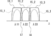
- FIG. 3 is a diagram for explaining a pass band of an optical filter included in the optical device according to the first embodiment.
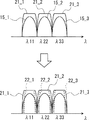
- 6 is a diagram for illustrating a problem in the first embodiment.
- FIG. 3 is a diagram for explaining a pass band of an optical filter included in the optical device according to the first embodiment.
- FIG. 3 is a diagram for explaining a pass band of an optical filter included in the optical device according to the first embodiment.
- FIG. 5 is a diagram for explaining an optical device according to a second embodiment;
- FIG. 6 is a diagram for explaining a bandwidth of a channel used in the optical device according to the second embodiment.
- 10 is a diagram for illustrating a problem in the second embodiment.
- FIG. FIG. 10 is a diagram for explaining a passband of a circulating AWG included in the optical device according to the second embodiment.
- FIG. 1 is a diagram for explaining an optical device according to the first embodiment.
- the optical device 1 according to the present embodiment includes a plurality of optical filters 11_1 to 11_3.
- Each of the optical filters 11_1 to 11_3 filters an optical signal in a predetermined band from among a plurality of optical signals having different wavelengths.
- the optical signals that have passed through the respective optical filters 11_1 to 11_3 are multiplexed by the multiplexing unit 12 and output from the optical device 1.
- the optical device 1 may be any optical device as long as it includes a plurality of optical filters that filter optical signals in a predetermined band from a plurality of optical signals having different wavelengths.
- Examples of such an optical device include, but are not limited to, a wavelength selective switch (WSS), an arrayed waveguide grating (AWG), a circular AWG, and the like. Absent. In FIG. 1, a circular AWG is illustrated as an example.
- FIG. 1 a functional block diagram is conceptually illustrated so that the contents of the present embodiment can be easily understood.
- the actual configuration of the optical device is not limited to this,
- the functions of the optical filters 11_1 to 11_3 and the function of the multiplexing unit 12 may be integrated.
- optical signals ⁇ 11 to ⁇ 13 are input to the input port P1
- optical signals ⁇ 21 to ⁇ 23 are input to the input port P2
- optical signals ⁇ 21 to ⁇ 23 are input to the input port P3.
- Optical signals ⁇ 31 to ⁇ 33 are respectively input.
- the optical signals ⁇ 11 to ⁇ 13 are optical signals having different wavelengths
- the optical signals ⁇ 21 to ⁇ 23 are optical signals having different wavelengths
- the optical signals ⁇ 31 to ⁇ 33 are optical signals having different wavelengths. .
- the optical signal ⁇ 11 input to the input port P1 the optical signal ⁇ 21 input to the input port P2, and the optical signal ⁇ 31 input to the input port P3 are optical signals having the same wavelength.
- the optical signal ⁇ 12 input to the input port P1, the optical signal ⁇ 22 input to the input port P2, and the optical signal ⁇ 32 input to the input port P3 are optical signals having the same wavelength.
- the optical signal ⁇ 13 input to the input port P1, the optical signal ⁇ 23 input to the input port P2, and the optical signal ⁇ 33 input to the input port P3 are optical signals having the same wavelength. Therefore, the optical filters 11_1 to 11_3 of the revolving AWG 1 filter the optical signals input to the input ports P1 to P3 so that optical signals with the same wavelength are not supplied to the multiplexing unit 12.
- the optical filter 11_1 passes the optical signal ⁇ 11 among the optical signals ⁇ 11 to ⁇ 13 input to the input port P1, and blocks the optical signals ⁇ 12 and ⁇ 13.
- the optical filter 11_2 passes the optical signal ⁇ 22 among the optical signals ⁇ 21 to ⁇ 23 input to the input port P2, and blocks the optical signals ⁇ 21 and ⁇ 23.
- the optical filter 11_3 passes the optical signal ⁇ 33 among the optical signals ⁇ 31 to ⁇ 33 input to the input port P3, and blocks the optical signals ⁇ 31 and ⁇ 32.
- the optical signal ⁇ 11 that has passed through the optical filter 11_1, the optical signal ⁇ 22 that has passed through the optical filter 11_2, and the optical signal ⁇ 33 that has passed through the optical filter 11_3 are multiplexed by the multiplexing unit 12 and output from the output port of the recursive AWG1.
- each of the optical filters 11_1 to 11_3 is configured such that a part of passbands of the respective optical filters that pass optical signals having wavelengths adjacent to each other overlap each other. That is, as shown in FIG. 2, the optical signal 15_1 ( ⁇ 11) and the optical signal 15_2 ( ⁇ 22) are adjacent to each other, and the passband 13_1 of the optical filter 11_1 and the passband 13_2 of the optical filter 11_2 are adjacent to each other. . And it is comprised so that a part of pass band 13_1 of the optical filter 11_1 and a part of pass band 13_2 of the optical filter 11_2 may mutually overlap (that is, the superimposition area
- the optical signal 15_2 ( ⁇ 22) and the optical signal 15_3 ( ⁇ 33) are adjacent to each other, and the pass band 13_2 of the optical filter 11_2 and the pass band 13_3 of the optical filter 11_3 are adjacent to each other. And it is comprised so that a part of pass band 13_2 of the optical filter 11_2 and a part of pass band 13_3 of the optical filter 11_3 may mutually overlap (that is, the superimposition area
- a recursive AWG When a recursive AWG is used as an optical device, for example, by adjusting the shape of the input / output waveguide of the recursive AWG and expanding the passband corresponding to each optical filter, the passband between adjacent ports can be increased. Can be superimposed.
- the passband of each port of the circulating AWG adjusts the shapes of the coupling part of the input waveguide of the circulating AWG and the slab waveguide on the input side, and the coupling part of the slab waveguide on the output side and the output waveguide. It can be expanded.
- the shape of the optical filter is not a rectangle, and the center frequency and the bandwidth have individual variations. Therefore, as the number of filters increases, the bandwidth of the filter seen at the receiving end becomes narrower. (Band narrowing). Due to such filter characteristics, both ends of the optical signal are cut off during the transmission process, and signal components are lost. Eventually, signal errors at the receiving end increase, and reception becomes impossible.
- the bandwidths of the pass bands 21_1 to 21_3 become narrower than the original bandwidths, and are as shown in the bandwidths 22_1 to 22_3. .
- both ends of each of the optical signals ⁇ 11, ⁇ 22, and ⁇ 33 are trimmed (the shaved portions are indicated by hatching), so that the optical signals ⁇ 11, ⁇ 22, and ⁇ 33 cannot be received.
- each of the optical filters 11_1 to 11_3 when configuring each of the optical filters 11_1 to 11_3, each of the optical filters that allow optical signals having wavelengths adjacent to each other to pass therethrough is provided. Some of the passbands overlap each other. That is, as shown in FIG. 2, a superposition region 17 is provided in which a part of the pass band 13_1 of the optical filter 11_1 and a part of the pass band 13_2 of the optical filter 11_2 are superposed. Further, an overlapping region 18 is provided in which a part of the pass band 13_2 of the optical filter 11_2 and a part of the pass band 13_3 of the optical filter 11_3 are overlapped. With such a configuration, it is possible to prevent both ends of the optical signals ⁇ 11, ⁇ 22, and ⁇ 33 from being scraped due to the band narrowing of the optical filter, and it is possible to suppress the generation of an optical signal that cannot be received.
- the passband width of each of the plurality of optical filters is increased while maintaining the frequency interval between the adjacent optical filters.
- the passband of the optical filter is changed from the passband 21_1 to 21_3 (see FIG. 3) to the passband 13_1 to 13_3 while maintaining the frequency interval of each optical filter.
- the frequency interval of each optical filter corresponds to the frequency interval between the peaks of the optical signals ⁇ 11, ⁇ 22, and ⁇ 33.
- the overlapping regions 17 and 18 can be provided in the passbands 13_1 to 13_3 of the respective optical filters 11_1 to 11_3.
- the shapes of the passbands 13_1 to 13_3 of the optical filters 11_1 to 11_3 can be arbitrary shapes.
- a super Gaussian type optical filter can be used as each of the optical filters 11_1 to 11_3.
- a superposition region can be provided in the pass band by adjusting the diffraction efficiency of the switch element (LCOS: Liquid crystal on silicon) of the wavelength selective switch WSS.
- LCOS Liquid crystal on silicon
- the bands of optical signals input to each port from the switch element 25 of the wavelength selective switch WSS do not overlap each other. Therefore, as shown in the left diagram of FIG. 4B, when the switching element 25 switches the optical signals ⁇ 11, ⁇ 22, and ⁇ 33 having different wavelengths to be input to the ports P1, P2, and P3, respectively, The signal bands do not overlap each other. Therefore, the switching element of the wavelength selective switch WSS performs switching so that the optical signals ⁇ 11, ⁇ 22, and ⁇ 33 are input to the ports P1, P2, and P3 in a state where they do not overlap each other.
- the switch element 25 of the wavelength selective switch WSS receives the optical signals ⁇ 11, ⁇ 22, and ⁇ 33 having different wavelengths respectively from the ports P1, P2, Output to P3. At this time, the switch element 25 performs switching so that the optical signals ⁇ 11, ⁇ 22, and ⁇ 33 do not overlap each other.
- the switch element 25 of the wavelength selective switch WSS adjusts the passband by the LCOS element.
- the LCOS element of the switch element 25 is set so as to have a pass band in which ends of the respective optical signals ⁇ 11, ⁇ 22, and ⁇ 33 overlap each other.
- the switch element 25 of the wavelength selective switch WSS of the present embodiment performs switching so that the ends of the optical signals ⁇ 11, ⁇ 22, and ⁇ 33 overlap each other as shown in the right diagram of FIG. 4B.
- the switch element 25 of the wavelength selective switch WSS superimposes the ends of the respective optical signals ⁇ 11, ⁇ 22, ⁇ 33 on each other. Switch. Specifically, the switch element 25 performs switching so that the optical signal ⁇ 11 is output to a part of the port P1 and the port P2.
- the switch element 25 performs switching so that the optical signal ⁇ 22 is output to a part of the port P1, the port P2, and a part of the port P3.
- the switch element 25 switches so that the optical signal ⁇ 33 is output to the port P3 and a part of the port P2.
- the part which the switch element 25 carries out overlap control of the optical signal is shown by hatching.
- the intensity P of each of the optical signals ⁇ 11, ⁇ 22, and ⁇ 33 is shown in the graph of FIG. 4B.
- switching can be performed so that the ends of the optical signals ⁇ 11, ⁇ 22, and ⁇ 33 overlap each other.
- FIG. 4B the case of the wavelength selective switch WSS with 1 input and N output (1 ⁇ N) is shown as an example, but this embodiment uses the wavelength selective switch WSS with N input and 1 output (N ⁇ 1). Can be realized.
- a superimposition region may be provided in the passband of each optical signal by adjusting the shape of the input / output waveguide of the AWG. For example, by adjusting the shape of the coupling portion between the AWG slab waveguide and the input / output waveguide, an overlapping region can be provided in the passband of each optical signal.
- the invention according to the present embodiment described above can provide an optical device capable of suppressing the optical signal from being cut by the band narrowing of the optical filter.
- the optical device 1 with three inputs and one output (circumferential AWG) is shown as an example.
- the present invention is not limited to this, and the number of input ports and the number of output ports of the optical device 1 are as follows. It can be arbitrarily determined. ⁇ Embodiment 2> Next, a second embodiment of the present invention will be described.
- FIG. 5 is a diagram for explaining the optical device 2 according to the second embodiment.
- the optical device 2 according to the present embodiment is configured using a plurality of beam splitters BS_1 to BS_3 and a plurality of circulating AWG_1 to AWG_3.
- the optical device 2 according to the present embodiment can be used for an optical node in an optical communication network, more specifically, an optical cross-connect node.
- the input sides of the beam splitters BS_1 to BS_3 are connected to three input side paths IN_ # 1 to IN_ # 3.
- the optical signals output from the beam splitters BS_1 to BS_3 are supplied to the circularity AWG_1 to AWG_3 provided at the subsequent stage of the beam splitters BS_1 to BS_3.
- the beam splitters BS_1 to BS_3 are one-input three-output (1 ⁇ 3) beam splitters, and the revolving AWG_1 to AWG_3 are three-input one-output (3 ⁇ 1) revolving AWGs.
- the output ports of the circulating AWG_1 to AWG_3 are connected to the output side paths OUT_ # 1 to OUT_ # 3, respectively.
- Each of the beam splitters BS_1 to BS_3 outputs each optical signal input to each of the beam splitters BS_1 to BS_3 to each input port of the circulating AWG_1 to AWG_3.
- the beam splitter BS_1 transmits the optical signals Ch11, Ch12, and Ch13 supplied from the input side path IN_ # 1 to the input port P1 of the revolving AWG_1, the input port P2 of the revolving AWG_2, and the revolving AWG_3. Supply to input port P3.
- the beam splitter BS_2 transmits the optical signals Ch21, Ch22, and Ch23 supplied from the input side path IN_ # 2 to the input port P2 of the circulatory AWG_1, the input port P3 of the circulatory AWG_2, and the input port of the circulatory AWG_3. Supply to P1.
- the beam splitter BS_3 converts the optical signals Ch31, Ch32, and Ch33 supplied from the input side path IN_ # 3 into an input port P3 for the recursive AWG_1, an input port P1 for the recursive AWG_2, and an input port for the recursive AWG_3. Supply to P2.
- Each of the circulating AWG_1 to AWG_3 filters each optical signal input to each of the input ports P1 to P3 and outputs it to the output side path. Specifically, the circulating AWG_1 outputs the optical signals Ch11, Ch32, and Ch23 among the optical signals input to the input ports P1 to P3 to the output side path OUT_ # 1. Further, the circulating AWG_2 outputs the optical signals Ch21, Ch12, and Ch33 among the optical signals input to the input ports P1 to P3 to the output side path OUT_ # 2. Further, the circulating AWG_3 outputs the optical signals Ch31, Ch22, and Ch13 among the optical signals input to the input ports P1 to P3 to the output side path OUT_ # 3.
- each of the optical signals Ch11, Ch12, and Ch13 passing through the input side path IN_ # 1 is an optical signal in a different frequency band.
- the optical signal Ch11 of the input side path IN_ # 1, the optical signal Ch21 of the input side path IN_ # 2, and the optical signal Ch31 of the input side path IN_ # 3 are optical signals in the same frequency band.
- the optical signal Ch12 of the input side path IN_ # 1, the optical signal Ch22 of the input side path IN_ # 2, and the optical signal Ch32 of the input side path IN_ # 3 are optical signals in the same frequency band.
- the optical signal Ch13 on the input side path IN_ # 1, the optical signal Ch23 on the input side path IN_ # 2, and the optical signal Ch33 on the input side path IN_ # 3 are optical signals in the same frequency band. For this reason, in order to realize WDM communication, it is necessary to prevent these optical signals from being output to the same output side route.
- each optical signal (Ch11, Ch12, Ch13,... Ch33) is routed in units of channels.
- a plurality of wavelength division multiplexed signals can be assigned within one channel band.
- FIG. 6 is a diagram for explaining the bandwidth of the channel used in the optical device 2 according to the present embodiment.
- a plurality of wavelength multiplexed signals (optical signals) 32 can be allocated in one channel band 31.
- FIG. 6 shows a case where the bandwidth of each channel Ch11, Ch12, and Ch13 is 150 GHz as an example, and three optical signals having a bandwidth of 50 GHz are assigned to the channel Ch11.
- a case is shown in which four optical signals having a bandwidth of 37.5 GHz are allocated to the channel Ch12.
- an optical signal having a bandwidth of 100 GHz and an optical signal having a bandwidth of 50 GHz are assigned to the channel Ch13.
- the example shown in FIG. 6 is an example, and the bandwidth of each channel band 31 can be arbitrarily determined. Further, the bandwidth and number of optical signals 32 allocated within the band of each channel can be arbitrarily determined.
- the pass bandwidth of each of the input ports P1 to P3 (that is, the bandwidth of the optical filter) of the circulating AWG_1 to AWG_3 is changed to the channel (Ch11, Ch12, Ch13,. ... Corresponding to the bandwidth of Ch33).
- an optical signal having a predetermined bandwidth that is, channels Ch11, Ch12, Ch13,...) Is obtained by expanding the pass bandwidth of each of the input ports P1 to P3 of the circulating AWG_1 to AWG_3 to the channel bandwidth. .. Ch33) can be filtered.
- three optical signals 32 having a bandwidth of 50 GHz can be filtered in the same direction.
- optical signals Ch11, Ch12, and Ch13 are supplied to the input port P1 of the circulating AWG_1, optical signals Ch21, Ch22, and Ch23 are supplied to the input port P2, and optical signals Ch31, Ch32, and Ch33 are supplied to the input port P3. Is supplied.
- the pass bandwidth of each of the input ports P1 to P3 it is possible to pass an optical signal having a bandwidth per channel of 150 GHz.
- the optical signals Ch21, Ch22, and Ch23 supplied to the input port P2 Only the signal Ch23 can be passed.
- the optical signals Ch31, Ch32, and Ch33 supplied to the input port P3 Only the signal Ch32 can be passed.
- the pass bandwidth of each of the input ports P1 to P3 of each of the cyclic AWGs 1 to AWG_3 may be m times the adjacent frequency interval of a plurality of wavelength multiplexed signals (m is a positive real number of 2 or more).
- m is a positive real number of 2 or more.
- the passband width of the input ports P1 to P3 is 150 GHz (see Ch12 in FIG. 6).
- communication with a capacity of 100 Gbps is performed with one optical signal
- four optical signals with a bandwidth of 37.5 GHz can be allocated to one channel, so communication with a capacity of 400 Gbps is realized. can do.
- the passband width of the input ports P1 to P3 is 150 GHz (see Ch11 in FIG. 6).
- the passband width of the input ports P1 to P3 is 150 GHz.
- the optical device 2 is configured to be able to assign a plurality of wavelength multiplexed signals within a band of one channel.
- the number and bandwidth of a plurality of wavelength division multiplexed signals allocated within one channel band can be arbitrarily set.
- the optical device 2 is configured such that a plurality of wavelength division multiplexed signals can be allocated within the band of one channel.
- the pass bandwidth of each input port of the cyclic AWG that is, the pass bandwidth of each optical filter corresponding to each input port so that the cyclic AWG can filter the optical signal on a channel basis.
- the optical signal to be transmitted can have flexibility. That is, as shown in FIG. 6, the number of optical signals allocated in one channel can be changed (refer to channels Ch11 and Ch12), and optical signals having different bandwidths can be allocated in one channel (channels). Ch13). Therefore, the optical signal to be transmitted can be given flexibility.
- the optical device 2 since the optical device 2 according to the present embodiment uses the circulating AWG_1 to AWG_3, it can be avoided that signals in the same frequency band are output to the same output side path.
- a plurality of wavelength multiplexed signals are allocated within a band of one channel.
- the bandwidth of the pass band 41 of the optical filter and the bandwidth of the four optical signals 42 that is, one channel
- the optical signal can be transmitted with high density.
- the shape of the optical filter is not rectangular, and there are individual variations in the center frequency and bandwidth, when the number of filters increases, the bandwidth of the filter seen at the receiving end becomes narrower (band narrowing). Due to such filter characteristics, both ends of the optical signal are cut off during the transmission process, and signal components are lost. Eventually, signal errors at the receiving end increase, and reception becomes impossible. More specifically, as shown in the lower diagram of FIG. 7, when the optical filters are connected in multiple stages, the bandwidth of the passband 41 becomes narrower than the original bandwidth, and the bandwidth 43 is shown. As a result, the signals at both ends of the four optical signals 42 are cut off (the cut portions are indicated by hatching), so that the signals at both ends may not be received.
- each of the pass bands of the optical filters that allow the optical signals of the channels adjacent to each other to pass each other overlap each other.
- An optical filter is configured. More specifically, a part of the pass band of the optical filter of the port P1 of the circular AWG_1 shown in FIG. 5 and a part of the pass band of the optical filter of the port P2 are the pass bands 51_1 and 51_2 shown in FIG. As shown in FIG. That is, the overlapping region 55 is provided in the pass band of the optical filter of the port P1 and the port P2 of the revolving AWG_1.
- the pass band of the optical filter of the port P1 of the recurring AWG_1 corresponds to the wavelength band of the channel Ch11. Further, the pass band of the optical filter of the port P2 of the circulating AWG_1 corresponds to the wavelength band of the channel Ch32.
- the passband of the circulating AWG optical filter can be made variable by adjusting the shape of the input / output waveguide of the circulating AWG, for example. By widening the pass band corresponding to each optical filter, it is possible to superimpose the pass band between the optical filters corresponding to adjacent ports.
- the passband corresponding to each port of the circulating AWG has the shape of the coupling part of the input waveguide of the circulating AWG and the input slab waveguide, and the coupling part of the output slab waveguide and output waveguide. It can be expanded by adjusting.
- a part of the pass band of the optical filter of the port P2 of the circular AWG_1 shown in FIG. 5 and a part of the pass band of the optical filter of the port P3 are mutually connected like pass bands 51_2 and 51_3 shown in FIG. It is configured to overlap. That is, the overlapping region 56 is provided in the pass band of the optical filter of the port P2 and the port P3 of the circulating AWG_1.
- the pass band of the optical filter of the port P2 of the circulating AWG_1 corresponds to the wavelength band of the channel Ch32.
- the pass band of the optical filter of the port P3 of the revolving AWG_1 corresponds to the wavelength band of the channel Ch23.
- the passband of each optical filter by extending the passband of each optical filter while maintaining the frequency interval of each optical filter corresponding to the channels adjacent to each other, a part of the passband of the optical filter corresponding to each channel adjacent to each other can be obtained. Can be superimposed.
- the width of the pass band 51_1 to 51_3 of the optical filter corresponding to each channel is changed from 150 GHz to 162.5 GHz while the frequency interval 54 of each channel is set to 150 GHz.
- the width of the overlapping region 55 where the pass band 51_1 and the pass band 51_2 overlap is 12.5 GHz.
- a part of the pass band 51_2 and a part of the pass band 51_3 can be superimposed.
- the width of the overlapping region 56 where the pass band 51_2 and the pass band 51_3 are overlapped is 12.5 GHz.
- each optical filter is arranged so that a part of the pass band of each optical filter that passes optical signals of channels adjacent to each other overlap each other. It is composed. Therefore, it is possible to suppress the both ends of the optical signal from being cut off in the transmission process due to the narrowing of the bandwidth of the optical signal, and it is possible to suppress the generation of an optical signal that cannot be received. Therefore, it is possible to suppress deterioration of transmission characteristics.
- the optical signal of another adjacent channel leaks and crosstalk occurs.
- the best transmission characteristics can be obtained by comparing the filter band narrowing and the crosstalk and optimizing the filter overlap width so that the degradation of the optical signal is minimized.
- the number of input side paths and output side paths may be other than this. That is, in the case of a configuration having n input side routes IN_ # 1 to IN_ # n and n output side routes OUT_ # 1 to OUT_ # n, the input side routes IN_ # 1 to IN_ # n N beam splitters BS_1 to BS_n (one input and n output beam splitters) connected to each other are provided. n is a natural number of 2 or more.
- n circular AWG_1 to AWG_n (circular AWG with n inputs and 1 output) are provided at the subsequent stage of the n beam splitters BS_1 to BS_n.
- Each of the n beam splitters BS_1 to BS_n outputs each optical signal input to each of the n beam splitters BS_1 to BS_n to each input port of the n circulating AWG_1 to AWG_n.
- Each of the n circulating AWG_1 to AWG_n filters each optical signal input to each input port and outputs it to the output side path. As a result, the routed optical signals are output to the output side paths OUT_ # 1 to OUT_ # n.
- the invention according to the present embodiment described above can provide an optical device capable of suppressing the optical signal from being cut by the band narrowing of the optical filter.
- Appendix 1 A plurality of optical filters that filter optical signals in a predetermined band from a plurality of optical signals having different wavelengths, The plurality of optical filters are configured such that a part of the passbands of the respective optical filters that pass optical signals of wavelengths adjacent to each other overlap each other.
- Optical device
- Appendix 3 The optical device according to appendix 1 or 2, wherein the plurality of optical filters are super Gaussian type optical filters or optical filters that can be approximated by a super Gaussian function.
- Appendix 4 The optical device according to any one of appendices 1 to 3, wherein the pass bandwidth per one of the plurality of optical filters is a bandwidth that allows a plurality of optical signals to pass through simultaneously.
- the optical device is a circular AWG that filters each of the optical signals; Each optical signal is filtered on a channel basis, The channel is configured to be able to assign a plurality of optical signals within the band of the channel, A pass bandwidth per one of the optical filters of the circulating AWG corresponds to a bandwidth of the channel; The optical device according to any one of appendices 1 to 4.
- Appendix 6 The optical device according to appendix 5, wherein a pass bandwidth per one of the optical filters of the circulating AWG is m times an adjacent frequency interval of the plurality of optical signals (m is a positive real number of 2 or more). .
- Appendix 7 The optical device according to appendix 6, wherein a pass bandwidth of each of the optical filters of the circulating AWG is 150 GHz and a center frequency interval is 150 GHz.
- Appendix 11 The optical device according to any one of appendices 1 to 3, wherein the optical device is a wavelength selective switch whose pass band is variable.
- Appendix 12 The optical device according to any one of appendices 1 to 3, wherein the optical device is an AWG.
- the wavelength-multiplexed optical signals are input to a plurality of optical filters in which a part of passbands for passing optical signals of wavelengths adjacent to each other are superimposed on each other, An optical signal processing method of filtering an optical signal in a predetermined band from a plurality of optical signals having different wavelengths.
- Appendix 14 Appendix 13 wherein a part of the passbands of each of the adjacent optical filters is overlapped with each other by widening the passband width of each of the plurality of optical filters while maintaining a frequency interval between the adjacent optical filters.
- Appendix 15 15. The optical signal processing method according to appendix 13 or 14, wherein the pass bandwidth per one of the plurality of optical filters is a bandwidth that allows a plurality of optical signals to pass through simultaneously.
- the optical filter is set so that a pass bandwidth when filtering each optical signal corresponds to a bandwidth of the channel in which a plurality of optical signals are allocated within a channel bandwidth, 16.
- Optical devices 11_1 to 11_3 Optical filter 12 Multiplexer 13_1 to 13_3 Pass band 15_1 to 15_3 Optical signal 17 and 18 Superimposed region 21_1 to 21_3 Pass band 22_1 to 22_3 Band width 31 Pass band 32 Optical signal 41 Pass band 42 Light Signal 43 Bandwidth 51_1 to 51_3 Passband 52 Optical signal 54 Frequency interval 55, 56 Overlapping region
Landscapes
- Physics & Mathematics (AREA)
- General Physics & Mathematics (AREA)
- Optics & Photonics (AREA)
- Engineering & Computer Science (AREA)
- Nonlinear Science (AREA)
- Computer Networks & Wireless Communication (AREA)
- Signal Processing (AREA)
- Electromagnetism (AREA)
- Microelectronics & Electronic Packaging (AREA)
- Optical Communication System (AREA)
- Optical Modulation, Optical Deflection, Nonlinear Optics, Optical Demodulation, Optical Logic Elements (AREA)
- Optical Integrated Circuits (AREA)
Abstract
Description
こうした光ファイバを使用した光通信システムでは、光ファイバ1本当たりの伝送効率を高めることが重要である。このため、複数の異なる波長の光信号を多重化して伝送する、波長分割多重(WDM:Wavelength Division Multiplex)通信が広く用いられている。
以下、図面を参照して本発明の実施の形態について説明する。
<実施の形態2>
次に、本発明の実施の形態2について説明する。
波長が異なる複数の光信号の中から所定の帯域の光信号をフィルタリングする光フィルタを複数備え、
前記複数の光フィルタは、互いに隣接する波長の光信号を各々通過させる各々の光フィルタの通過帯域の一部が互いに重畳するように構成されている、
光デバイス。
隣接する光フィルタ間の周波数間隔を維持しつつ前記複数の光フィルタの各々の通過帯域幅を広げることで、前記隣接する光フィルタの各々の通過帯域の一部を互いに重畳させる、付記1に記載の光デバイス。
前記複数の光フィルタは、スーパーガウシアン型の光フィルタまたはスーパーガウシアン関数で近似可能な光フィルタである、付記1または2に記載の光デバイス。
前記複数の光フィルタの1つの当たりの通過帯域幅は、複数の光信号を同時に通過させることができる帯域幅である、付記1乃至3のいずれか一項に記載の光デバイス。
前記光デバイスは、前記各々の光信号をフィルタリングする周回性AWGであり、
前記各々の光信号はチャネル単位でフィルタリングされ、
前記チャネルは、当該チャネルの帯域内に複数の光信号を割り当て可能に構成されており、
前記周回性AWGの前記光フィルタの1つの当たりの通過帯域幅は前記チャネルの帯域幅に対応している、
付記1乃至4のいずれか一項に記載の光デバイス。
前記周回性AWGの前記光フィルタの1つ当たりの通過帯域幅は、前記複数の光信号の隣接周波数間隔のm倍(mは2以上の正の実数)である、付記5に記載の光デバイス。
前記周回性AWGの前記各々の光フィルタの通過帯域幅は150GHzで、中心周波数間隔は150GHzである、付記6に記載の光デバイス。
前記隣接周波数間隔は37.5GHzであり、前記mの値はm=4である、付記7に記載の光デバイス。
前記隣接周波数間隔は50GHzであり、前記mの値はm=3である、付記7に記載の光デバイス。
前記隣接周波数間隔は75GHzであり、前記mの値はm=2である、付記7に記載の光デバイス。
前記光デバイスは通過帯域が可変可能な波長選択スイッチである、付記1乃至3のいずれか一項に記載の光デバイス。
前記光デバイスはAWGである、付記1乃至3のいずれか一項に記載の光デバイス。
互いに隣接する波長の光信号を各々通過させる通過帯域の一部が互いに重畳している複数の光フィルタに、波長多重化された光信号を入力し、
波長が異なる複数の前記光信号の中から所定の帯域の光信号をフィルタリングする、光信号の処理方法。
隣接する前記光フィルタ間の周波数間隔を維持しつつ前記複数の光フィルタの各々の通過帯域幅を広げることで、前記隣接する光フィルタの各々の通過帯域の一部を互いに重畳させる、付記13に記載の光信号の処理方法。
前記複数の光フィルタの1つの当たりの通過帯域幅は、複数の光信号を同時に通過させることができる帯域幅である、付記13または14に記載の光信号の処理方法。
前記光フィルタは、前記各々の光信号をフィルタリングする際の通過帯域幅がチャネルの帯域内に複数の光信号が割り当てられている前記チャネルの帯域幅に対応するように設定され、
前記各々の光信号を前記チャネル単位でフィルタリングする、付記13乃至15に記載の光信号の処理方法。
11_1~11_3 光フィルタ
12 合波部
13_1~13_3 通過帯域
15_1~15_3 光信号
17、18 重畳領域
21_1~21_3 通過帯域
22_1~22_3 帯域幅
31 通過帯域
32 光信号
41 通過帯域
42 光信号
43 帯域幅
51_1~51_3 通過帯域
52 光信号
54 周波数間隔
55、56 重畳領域
Claims (16)
- 波長が異なる複数の光信号の中から所定の帯域の光信号をフィルタリングする光フィルタを複数備え、
前記複数の光フィルタは、互いに隣接する波長の光信号を各々通過させる各々の光フィルタの通過帯域の一部が互いに重畳するように構成されている、
光デバイス。 - 隣接する光フィルタ間の周波数間隔を維持しつつ前記複数の光フィルタの各々の通過帯域幅を広げることで、前記隣接する光フィルタの各々の通過帯域の一部を互いに重畳させる、請求項1に記載の光デバイス。
- 前記複数の光フィルタは、スーパーガウシアン型の光フィルタまたはスーパーガウシアン関数で近似可能な光フィルタである、請求項1または2に記載の光デバイス。
- 前記複数の光フィルタの1つの当たりの通過帯域幅は、複数の光信号を同時に通過させることができる帯域幅である、請求項1乃至3のいずれか一項に記載の光デバイス。
- 前記光デバイスは、前記各々の光信号をフィルタリングする周回性AWGであり、
前記各々の光信号はチャネル単位でフィルタリングされ、
前記チャネルは、当該チャネルの帯域内に複数の光信号を割り当て可能に構成されており、
前記周回性AWGの前記光フィルタの1つの当たりの通過帯域幅は前記チャネルの帯域幅に対応している、
請求項1乃至4のいずれか一項に記載の光デバイス。 - 前記周回性AWGの前記光フィルタの1つ当たりの通過帯域幅は、前記複数の光信号の隣接周波数間隔のm倍(mは2以上の正の実数)である、請求項5に記載の光デバイス。
- 前記周回性AWGの前記各々の光フィルタの通過帯域幅は150GHzで、中心周波数間隔は150GHzである、請求項6に記載の光デバイス。
- 前記隣接周波数間隔は37.5GHzであり、前記mの値はm=4である、請求項7に記載の光デバイス。
- 前記隣接周波数間隔は50GHzであり、前記mの値はm=3である、請求項7に記載の光デバイス。
- 前記隣接周波数間隔は75GHzであり、前記mの値はm=2である、請求項7に記載の光デバイス。
- 前記光デバイスは通過帯域が可変可能な波長選択スイッチである、請求項1乃至3のいずれか一項に記載の光デバイス。
- 前記光デバイスはAWGである、請求項1乃至3のいずれか一項に記載の光デバイス。
- 互いに隣接する波長の光信号を各々通過させる通過帯域の一部が互いに重畳している複数の光フィルタに、波長多重化された光信号を入力し、
波長が異なる複数の前記光信号の中から所定の帯域の光信号をフィルタリングする、光信号の処理方法。 - 隣接する前記光フィルタ間の周波数間隔を維持しつつ前記複数の光フィルタの各々の通過帯域幅を広げることで、前記隣接する光フィルタの各々の通過帯域の一部を互いに重畳させる、請求項13に記載の光信号の処理方法。
- 前記複数の光フィルタの1つの当たりの通過帯域幅は、複数の光信号を同時に通過させることができる帯域幅である、請求項13または14に記載の光信号の処理方法。
- 前記光フィルタは、前記各々の光信号をフィルタリングする際の通過帯域幅がチャネルの帯域内に複数の光信号が割り当てられている前記チャネルの帯域幅に対応するように設定され、
前記各々の光信号を前記チャネル単位でフィルタリングする、請求項13乃至15のいずれか一項に記載の光信号の処理方法。
Priority Applications (4)
| Application Number | Priority Date | Filing Date | Title |
|---|---|---|---|
| US16/078,980 US10539741B2 (en) | 2016-02-29 | 2017-02-21 | Optical device with optical filters and processing method of optical signals |
| CN201780013307.7A CN109313309B (zh) | 2016-02-29 | 2017-02-21 | 光学装置 |
| JP2018503058A JP6763424B2 (ja) | 2016-02-29 | 2017-02-21 | 光デバイス |
| EP17759744.0A EP3425434A4 (en) | 2016-02-29 | 2017-02-21 | OPTICAL DEVICE |
Applications Claiming Priority (2)
| Application Number | Priority Date | Filing Date | Title |
|---|---|---|---|
| JP2016-038163 | 2016-02-29 | ||
| JP2016038163 | 2016-02-29 |
Publications (1)
| Publication Number | Publication Date |
|---|---|
| WO2017150278A1 true WO2017150278A1 (ja) | 2017-09-08 |
Family
ID=59742805
Family Applications (1)
| Application Number | Title | Priority Date | Filing Date |
|---|---|---|---|
| PCT/JP2017/006394 Ceased WO2017150278A1 (ja) | 2016-02-29 | 2017-02-21 | 光デバイス |
Country Status (5)
| Country | Link |
|---|---|
| US (1) | US10539741B2 (ja) |
| EP (1) | EP3425434A4 (ja) |
| JP (1) | JP6763424B2 (ja) |
| CN (1) | CN109313309B (ja) |
| WO (1) | WO2017150278A1 (ja) |
Cited By (4)
| Publication number | Priority date | Publication date | Assignee | Title |
|---|---|---|---|---|
| CN109067472A (zh) * | 2018-08-23 | 2018-12-21 | 东南大学 | 一种基于重叠覆盖滤光片组的多色光信号接收方法 |
| WO2019091326A1 (en) * | 2017-11-10 | 2019-05-16 | Huawei Technologies Co., Ltd. | Wide passband wavelength selective switch |
| WO2020049791A1 (ja) | 2018-09-07 | 2020-03-12 | 日本電気株式会社 | 光伝送装置、光通信システム及び光信号の伝送方法 |
| US11018763B2 (en) | 2019-08-30 | 2021-05-25 | Fujitsu Limited | Network system, management device, and management method |
Families Citing this family (3)
| Publication number | Priority date | Publication date | Assignee | Title |
|---|---|---|---|---|
| EP3425827B1 (en) * | 2016-02-29 | 2021-01-20 | Nec Corporation | Optical transmission device |
| JP6988296B2 (ja) * | 2017-09-14 | 2022-01-05 | 富士通株式会社 | 伝送装置及び信号監視方法 |
| US12425753B2 (en) * | 2022-02-02 | 2025-09-23 | Infinera Corp. | Grouping of optical passbands for loading in an optical transmission spectrum using an affinity identifier |
Citations (6)
| Publication number | Priority date | Publication date | Assignee | Title |
|---|---|---|---|---|
| JP2000244402A (ja) * | 1999-02-19 | 2000-09-08 | Jds Uniphase Inc | 光システム |
| JP2004040253A (ja) * | 2002-06-28 | 2004-02-05 | Fujitsu Ltd | 波長多重光伝送システムおよび波長多重光伝送方法 |
| JP2012175247A (ja) * | 2011-02-18 | 2012-09-10 | Nippon Telegr & Teleph Corp <Ntt> | 波長調整システム及び方法 |
| US20140268155A1 (en) * | 2013-03-14 | 2014-09-18 | Intelligent Fiber Optic Systems, Inc. | AWG Filter for Wavelength Interrogator |
| JP2015019289A (ja) | 2013-07-11 | 2015-01-29 | 富士通株式会社 | 光伝送装置、光伝送システム、及び光伝送方法 |
| JP2015060125A (ja) * | 2013-09-19 | 2015-03-30 | 日本電信電話株式会社 | 光可変フィルタ |
Family Cites Families (12)
| Publication number | Priority date | Publication date | Assignee | Title |
|---|---|---|---|---|
| US5412744A (en) * | 1994-05-02 | 1995-05-02 | At&T Corp. | Frequency routing device having a wide and substantially flat passband |
| JPH09321701A (ja) * | 1996-05-31 | 1997-12-12 | Fujitsu Ltd | 光通信システム及び光増幅器 |
| EP0936483A3 (en) * | 1998-02-10 | 1999-09-22 | Lucent Technologies Inc. | Optical router with coherent connecting paths |
| JP4647074B2 (ja) * | 2000-10-04 | 2011-03-09 | 富士通株式会社 | 波長多重光通信システム |
| JP4622168B2 (ja) * | 2001-06-22 | 2011-02-02 | 住友電気工業株式会社 | 波長多重信号光監視装置、監視方法、及び光伝送システム |
| WO2003009508A1 (en) * | 2001-07-19 | 2003-01-30 | Novx Systems Inc. | Optical add/drop switch |
| JP5691255B2 (ja) * | 2010-06-22 | 2015-04-01 | 富士通株式会社 | Osnr測定装置および光通信システム |
| CN102695101B (zh) * | 2011-03-21 | 2015-11-18 | 苏州海光芯创光电科技有限公司 | 一种波分复用上的无源光网络 |
| US9160455B2 (en) * | 2011-07-14 | 2015-10-13 | Applied Optoelectronics, Inc. | External cavity laser array system and WDM optical system including same |
| GB201119922D0 (en) * | 2011-11-18 | 2012-01-04 | Cambridge Entpr Ltd | Optical signal transmission systems |
| JP5962455B2 (ja) * | 2012-11-21 | 2016-08-03 | 富士通株式会社 | 光伝送装置、ノード装置、光伝送方法および光伝送システム |
| CN104092538B (zh) * | 2014-07-15 | 2017-04-12 | 华南师范大学 | 多用户波分复用qkd网络系统及其密钥分发与共享方法 |
-
2017
- 2017-02-21 CN CN201780013307.7A patent/CN109313309B/zh active Active
- 2017-02-21 JP JP2018503058A patent/JP6763424B2/ja active Active
- 2017-02-21 WO PCT/JP2017/006394 patent/WO2017150278A1/ja not_active Ceased
- 2017-02-21 US US16/078,980 patent/US10539741B2/en active Active
- 2017-02-21 EP EP17759744.0A patent/EP3425434A4/en not_active Withdrawn
Patent Citations (6)
| Publication number | Priority date | Publication date | Assignee | Title |
|---|---|---|---|---|
| JP2000244402A (ja) * | 1999-02-19 | 2000-09-08 | Jds Uniphase Inc | 光システム |
| JP2004040253A (ja) * | 2002-06-28 | 2004-02-05 | Fujitsu Ltd | 波長多重光伝送システムおよび波長多重光伝送方法 |
| JP2012175247A (ja) * | 2011-02-18 | 2012-09-10 | Nippon Telegr & Teleph Corp <Ntt> | 波長調整システム及び方法 |
| US20140268155A1 (en) * | 2013-03-14 | 2014-09-18 | Intelligent Fiber Optic Systems, Inc. | AWG Filter for Wavelength Interrogator |
| JP2015019289A (ja) | 2013-07-11 | 2015-01-29 | 富士通株式会社 | 光伝送装置、光伝送システム、及び光伝送方法 |
| JP2015060125A (ja) * | 2013-09-19 | 2015-03-30 | 日本電信電話株式会社 | 光可変フィルタ |
Non-Patent Citations (5)
| Title |
|---|
| JINNO, M. ET AL.: "Demonstration of Novel Spectrum-Efficient Elastic Optical Path Network with Per-Channel Variable Capacity of 40 Gb/s to Over 400 Gb/s", 34 TH EUROPEAN CONFERENCE ON OPTICAL COMMUNICATION, 24 September 2008 (2008-09-24), pages 1 - 2, XP031381357 * |
| KLONIDIS, D. ET AL.: "Enabling Transparent Technologies for the Development of Highly Granular Flexible Optical Cross-Connects", 2014 16TH INTERNATIONAL CONFERENCE ON TRANSPARENT OPTICAL NETWORKS (ICTON), 6 July 2014 (2014-07-06), pages 1 - 6, XP032627193 * |
| See also references of EP3425434A4 |
| YURIE MATSUYAMA ET AL.: "Proposition of Simplified OXC Architecture on Elastic Optical Node", PROCEEDINGS OF THE 2016 IEICE GENERAL CONFERENCE, 1 March 2016 (2016-03-01), pages 311, XP009512354 * |
| ZAMI, T.: "Impact of intra-superchannel spectral constraints on the throughput of the elastic WDM networks", OPTICAL FIBER COMMUNICATION CONFERENCE AND EXPOSITION (OFC/NFOEC), 2012 AND THE NATIONAL FIBER OPTIC ENGINEERS CONFERENCE, 3 May 2012 (2012-05-03), pages 1 - 3, XP032174957 * |
Cited By (7)
| Publication number | Priority date | Publication date | Assignee | Title |
|---|---|---|---|---|
| WO2019091326A1 (en) * | 2017-11-10 | 2019-05-16 | Huawei Technologies Co., Ltd. | Wide passband wavelength selective switch |
| US10701465B2 (en) | 2017-11-10 | 2020-06-30 | Huawei Technologies Co., Ltd. | Wide passband wavelength selective switch |
| CN109067472A (zh) * | 2018-08-23 | 2018-12-21 | 东南大学 | 一种基于重叠覆盖滤光片组的多色光信号接收方法 |
| CN109067472B (zh) * | 2018-08-23 | 2021-09-07 | 东南大学 | 一种基于重叠覆盖滤光片组的多色光信号接收方法 |
| WO2020049791A1 (ja) | 2018-09-07 | 2020-03-12 | 日本電気株式会社 | 光伝送装置、光通信システム及び光信号の伝送方法 |
| US11336375B2 (en) | 2018-09-07 | 2022-05-17 | Nec Corporation | Optical transmission apparatus, optical communication system, and optical signal transmission method |
| US11018763B2 (en) | 2019-08-30 | 2021-05-25 | Fujitsu Limited | Network system, management device, and management method |
Also Published As
| Publication number | Publication date |
|---|---|
| EP3425434A1 (en) | 2019-01-09 |
| JP6763424B2 (ja) | 2020-09-30 |
| CN109313309B (zh) | 2021-01-12 |
| CN109313309A (zh) | 2019-02-05 |
| JPWO2017150278A1 (ja) | 2018-12-06 |
| US10539741B2 (en) | 2020-01-21 |
| US20190064437A1 (en) | 2019-02-28 |
| EP3425434A4 (en) | 2019-10-30 |
Similar Documents
| Publication | Publication Date | Title |
|---|---|---|
| JP6763424B2 (ja) | 光デバイス | |
| JP5176598B2 (ja) | 光分岐挿入装置および光伝送装置 | |
| JP4587792B2 (ja) | リング状光伝送システムおよびこれに接続される光装置 | |
| JP4528922B2 (ja) | フレキシブル波長バンドアグリゲータ、デアグリゲータおよび階層的ハイブリッド光クロスコネクトシステム | |
| US8903242B2 (en) | Directionless and colorless reconfigurable optical add/drop multiplexer | |
| JP4843659B2 (ja) | 光伝送ネットワークシステム、光伝送装置、及びそれらを用いた通過帯域割り当て方法 | |
| JP5807338B2 (ja) | 光伝送装置および光フィルタ回路 | |
| US10097304B2 (en) | Optical switch, an optical switching apparatus, an optical communications network node and an optical communications network | |
| JP4152932B2 (ja) | 光分波方法および光合波方法、並びに、それを用いた光伝送装置 | |
| WO2016030225A1 (en) | Reconfigurable add/drop multiplexing in optical networks | |
| JP6419154B2 (ja) | 光ネットワーク | |
| JP6645571B2 (ja) | 光伝送装置 | |
| JP3574754B2 (ja) | 光パスクロスコネクト装置 | |
| CN104160645B (zh) | 利用融合信号添加和移除的多频带可重配置光学分插复用 | |
| JP4176608B2 (ja) | 光通信ネットワークシステム及びその波長ルーティング装置 | |
| EP4529054A1 (en) | Partially colored flexgrid wavelength-division multiplexer/demultiplexer | |
| JP2008219553A (ja) | 光ノード、および光ノードの制御方法 | |
| WO2015144869A1 (en) | A wavelength routing cross-connect | |
| JP2011203539A (ja) | 波長変換システム及び波長変換方法 |
Legal Events
| Date | Code | Title | Description |
|---|---|---|---|
| WWE | Wipo information: entry into national phase |
Ref document number: 2018503058 Country of ref document: JP |
|
| NENP | Non-entry into the national phase |
Ref country code: DE |
|
| WWE | Wipo information: entry into national phase |
Ref document number: 2017759744 Country of ref document: EP |
|
| ENP | Entry into the national phase |
Ref document number: 2017759744 Country of ref document: EP Effective date: 20181001 |
|
| 121 | Ep: the epo has been informed by wipo that ep was designated in this application |
Ref document number: 17759744 Country of ref document: EP Kind code of ref document: A1 |