WO2017154232A1 - Dispositif à semi-conducteurs et grille de connexion - Google Patents
Dispositif à semi-conducteurs et grille de connexion Download PDFInfo
- Publication number
- WO2017154232A1 WO2017154232A1 PCT/JP2016/070664 JP2016070664W WO2017154232A1 WO 2017154232 A1 WO2017154232 A1 WO 2017154232A1 JP 2016070664 W JP2016070664 W JP 2016070664W WO 2017154232 A1 WO2017154232 A1 WO 2017154232A1
- Authority
- WO
- WIPO (PCT)
- Prior art keywords
- wiring board
- output
- boards
- power supply
- terminal plates
- Prior art date
- Legal status (The legal status is an assumption and is not a legal conclusion. Google has not performed a legal analysis and makes no representation as to the accuracy of the status listed.)
- Ceased
Links
Images


Classifications
-
- H—ELECTRICITY
- H10—SEMICONDUCTOR DEVICES; ELECTRIC SOLID-STATE DEVICES NOT OTHERWISE PROVIDED FOR
- H10W—GENERIC PACKAGES, INTERCONNECTIONS, CONNECTORS OR OTHER CONSTRUCTIONAL DETAILS OF DEVICES COVERED BY CLASS H10
- H10W70/00—Package substrates; Interposers; Redistribution layers [RDL]
- H10W70/40—Leadframes
- H10W70/461—Leadframes specially adapted for cooling
-
- H—ELECTRICITY
- H10—SEMICONDUCTOR DEVICES; ELECTRIC SOLID-STATE DEVICES NOT OTHERWISE PROVIDED FOR
- H10W—GENERIC PACKAGES, INTERCONNECTIONS, CONNECTORS OR OTHER CONSTRUCTIONAL DETAILS OF DEVICES COVERED BY CLASS H10
- H10W70/00—Package substrates; Interposers; Redistribution layers [RDL]
- H10W70/40—Leadframes
- H10W70/421—Shapes or dispositions
-
- H—ELECTRICITY
- H10—SEMICONDUCTOR DEVICES; ELECTRIC SOLID-STATE DEVICES NOT OTHERWISE PROVIDED FOR
- H10W—GENERIC PACKAGES, INTERCONNECTIONS, CONNECTORS OR OTHER CONSTRUCTIONAL DETAILS OF DEVICES COVERED BY CLASS H10
- H10W70/00—Package substrates; Interposers; Redistribution layers [RDL]
- H10W70/40—Leadframes
- H10W70/421—Shapes or dispositions
- H10W70/424—Cross-sectional shapes
- H10W70/427—Bent parts
- H10W70/429—Bent parts being the outer leads
-
- H—ELECTRICITY
- H10—SEMICONDUCTOR DEVICES; ELECTRIC SOLID-STATE DEVICES NOT OTHERWISE PROVIDED FOR
- H10W—GENERIC PACKAGES, INTERCONNECTIONS, CONNECTORS OR OTHER CONSTRUCTIONAL DETAILS OF DEVICES COVERED BY CLASS H10
- H10W70/00—Package substrates; Interposers; Redistribution layers [RDL]
- H10W70/40—Leadframes
- H10W70/421—Shapes or dispositions
- H10W70/442—Shapes or dispositions of multiple leadframes in a single chip
-
- H—ELECTRICITY
- H10—SEMICONDUCTOR DEVICES; ELECTRIC SOLID-STATE DEVICES NOT OTHERWISE PROVIDED FOR
- H10W—GENERIC PACKAGES, INTERCONNECTIONS, CONNECTORS OR OTHER CONSTRUCTIONAL DETAILS OF DEVICES COVERED BY CLASS H10
- H10W70/00—Package substrates; Interposers; Redistribution layers [RDL]
- H10W70/40—Leadframes
- H10W70/464—Additional interconnections in combination with leadframes
- H10W70/465—Bumps or wires
-
- H—ELECTRICITY
- H10—SEMICONDUCTOR DEVICES; ELECTRIC SOLID-STATE DEVICES NOT OTHERWISE PROVIDED FOR
- H10W—GENERIC PACKAGES, INTERCONNECTIONS, CONNECTORS OR OTHER CONSTRUCTIONAL DETAILS OF DEVICES COVERED BY CLASS H10
- H10W70/00—Package substrates; Interposers; Redistribution layers [RDL]
- H10W70/40—Leadframes
- H10W70/464—Additional interconnections in combination with leadframes
- H10W70/466—Tape carriers or flat leads
-
- H—ELECTRICITY
- H10—SEMICONDUCTOR DEVICES; ELECTRIC SOLID-STATE DEVICES NOT OTHERWISE PROVIDED FOR
- H10W—GENERIC PACKAGES, INTERCONNECTIONS, CONNECTORS OR OTHER CONSTRUCTIONAL DETAILS OF DEVICES COVERED BY CLASS H10
- H10W70/00—Package substrates; Interposers; Redistribution layers [RDL]
- H10W70/40—Leadframes
- H10W70/475—Capacitors in combination with leadframes
-
- H—ELECTRICITY
- H10—SEMICONDUCTOR DEVICES; ELECTRIC SOLID-STATE DEVICES NOT OTHERWISE PROVIDED FOR
- H10W—GENERIC PACKAGES, INTERCONNECTIONS, CONNECTORS OR OTHER CONSTRUCTIONAL DETAILS OF DEVICES COVERED BY CLASS H10
- H10W70/00—Package substrates; Interposers; Redistribution layers [RDL]
- H10W70/40—Leadframes
- H10W70/481—Leadframes for devices being provided for in groups H10D8/00 - H10D48/00
-
- H—ELECTRICITY
- H10—SEMICONDUCTOR DEVICES; ELECTRIC SOLID-STATE DEVICES NOT OTHERWISE PROVIDED FOR
- H10W—GENERIC PACKAGES, INTERCONNECTIONS, CONNECTORS OR OTHER CONSTRUCTIONAL DETAILS OF DEVICES COVERED BY CLASS H10
- H10W74/00—Encapsulations, e.g. protective coatings
- H10W74/10—Encapsulations, e.g. protective coatings characterised by their shape or disposition
- H10W74/111—Encapsulations, e.g. protective coatings characterised by their shape or disposition the semiconductor body being completely enclosed
- H10W74/114—Encapsulations, e.g. protective coatings characterised by their shape or disposition the semiconductor body being completely enclosed by a substrate and the encapsulations
-
- H—ELECTRICITY
- H10—SEMICONDUCTOR DEVICES; ELECTRIC SOLID-STATE DEVICES NOT OTHERWISE PROVIDED FOR
- H10W—GENERIC PACKAGES, INTERCONNECTIONS, CONNECTORS OR OTHER CONSTRUCTIONAL DETAILS OF DEVICES COVERED BY CLASS H10
- H10W90/00—Package configurations
-
- H—ELECTRICITY
- H10—SEMICONDUCTOR DEVICES; ELECTRIC SOLID-STATE DEVICES NOT OTHERWISE PROVIDED FOR
- H10W—GENERIC PACKAGES, INTERCONNECTIONS, CONNECTORS OR OTHER CONSTRUCTIONAL DETAILS OF DEVICES COVERED BY CLASS H10
- H10W90/00—Package configurations
- H10W90/811—Multiple chips on leadframes
-
- H—ELECTRICITY
- H10—SEMICONDUCTOR DEVICES; ELECTRIC SOLID-STATE DEVICES NOT OTHERWISE PROVIDED FOR
- H10W—GENERIC PACKAGES, INTERCONNECTIONS, CONNECTORS OR OTHER CONSTRUCTIONAL DETAILS OF DEVICES COVERED BY CLASS H10
- H10W72/00—Interconnections or connectors in packages
- H10W72/071—Connecting or disconnecting
- H10W72/075—Connecting or disconnecting of bond wires
- H10W72/07551—Connecting or disconnecting of bond wires characterised by changes in properties of the bond wires during the connecting
- H10W72/07552—Connecting or disconnecting of bond wires characterised by changes in properties of the bond wires during the connecting changes in structures or sizes
-
- H—ELECTRICITY
- H10—SEMICONDUCTOR DEVICES; ELECTRIC SOLID-STATE DEVICES NOT OTHERWISE PROVIDED FOR
- H10W—GENERIC PACKAGES, INTERCONNECTIONS, CONNECTORS OR OTHER CONSTRUCTIONAL DETAILS OF DEVICES COVERED BY CLASS H10
- H10W72/00—Interconnections or connectors in packages
- H10W72/50—Bond wires
- H10W72/521—Structures or relative sizes of bond wires
- H10W72/527—Multiple bond wires having different sizes
-
- H—ELECTRICITY
- H10—SEMICONDUCTOR DEVICES; ELECTRIC SOLID-STATE DEVICES NOT OTHERWISE PROVIDED FOR
- H10W—GENERIC PACKAGES, INTERCONNECTIONS, CONNECTORS OR OTHER CONSTRUCTIONAL DETAILS OF DEVICES COVERED BY CLASS H10
- H10W72/00—Interconnections or connectors in packages
- H10W72/50—Bond wires
- H10W72/541—Dispositions of bond wires
- H10W72/547—Dispositions of multiple bond wires
- H10W72/5475—Dispositions of multiple bond wires multiple bond wires connected to common bond pads at both ends of the wires
-
- H—ELECTRICITY
- H10—SEMICONDUCTOR DEVICES; ELECTRIC SOLID-STATE DEVICES NOT OTHERWISE PROVIDED FOR
- H10W—GENERIC PACKAGES, INTERCONNECTIONS, CONNECTORS OR OTHER CONSTRUCTIONAL DETAILS OF DEVICES COVERED BY CLASS H10
- H10W72/00—Interconnections or connectors in packages
- H10W72/851—Dispositions of multiple connectors or interconnections
- H10W72/853—On the same surface
- H10W72/871—Bond wires and strap connectors
-
- H—ELECTRICITY
- H10—SEMICONDUCTOR DEVICES; ELECTRIC SOLID-STATE DEVICES NOT OTHERWISE PROVIDED FOR
- H10W—GENERIC PACKAGES, INTERCONNECTIONS, CONNECTORS OR OTHER CONSTRUCTIONAL DETAILS OF DEVICES COVERED BY CLASS H10
- H10W72/00—Interconnections or connectors in packages
- H10W72/90—Bond pads, in general
- H10W72/921—Structures or relative sizes of bond pads
- H10W72/926—Multiple bond pads having different sizes
-
- H—ELECTRICITY
- H10—SEMICONDUCTOR DEVICES; ELECTRIC SOLID-STATE DEVICES NOT OTHERWISE PROVIDED FOR
- H10W—GENERIC PACKAGES, INTERCONNECTIONS, CONNECTORS OR OTHER CONSTRUCTIONAL DETAILS OF DEVICES COVERED BY CLASS H10
- H10W74/00—Encapsulations, e.g. protective coatings
- H10W74/10—Encapsulations, e.g. protective coatings characterised by their shape or disposition
-
- H—ELECTRICITY
- H10—SEMICONDUCTOR DEVICES; ELECTRIC SOLID-STATE DEVICES NOT OTHERWISE PROVIDED FOR
- H10W—GENERIC PACKAGES, INTERCONNECTIONS, CONNECTORS OR OTHER CONSTRUCTIONAL DETAILS OF DEVICES COVERED BY CLASS H10
- H10W90/00—Package configurations
- H10W90/701—Package configurations characterised by the relative positions of pads or connectors relative to package parts
- H10W90/751—Package configurations characterised by the relative positions of pads or connectors relative to package parts of bond wires
- H10W90/756—Package configurations characterised by the relative positions of pads or connectors relative to package parts of bond wires between a chip and a stacked lead frame, conducting package substrate or heat sink
-
- H—ELECTRICITY
- H10—SEMICONDUCTOR DEVICES; ELECTRIC SOLID-STATE DEVICES NOT OTHERWISE PROVIDED FOR
- H10W—GENERIC PACKAGES, INTERCONNECTIONS, CONNECTORS OR OTHER CONSTRUCTIONAL DETAILS OF DEVICES COVERED BY CLASS H10
- H10W90/00—Package configurations
- H10W90/701—Package configurations characterised by the relative positions of pads or connectors relative to package parts
- H10W90/761—Package configurations characterised by the relative positions of pads or connectors relative to package parts of strap connectors
- H10W90/766—Package configurations characterised by the relative positions of pads or connectors relative to package parts of strap connectors between a chip and a stacked lead frame, conducting package substrate or heat sink
Definitions
- the present invention relates to a semiconductor device and a lead frame.
- This application claims priority based on international application PCT / JP2016 / 057776 filed in Japan on March 11, 2016, the contents of which are incorporated herein by reference.
- a semiconductor device in which an external connection terminal portion (terminal plate) protruding from a sealing resin is integrally formed on an electrode plate exposed on the lower surface of the sealing resin (for example, Patent Document 1).
- the base end portion of the external connection terminal portion extends in parallel with the electrode plate, and functions as a heat dissipation surface together with the lower surface of the electrode plate.
- the width dimension of the external connection terminal portion is constant from the base end portion to the tip end portion. For this reason, when a plurality of external connection terminal portions are arranged, the external connection terminal portions are considered in consideration of the pitch between adjacent external connection terminal portions (particularly, the pitch between the tips of adjacent external connection terminal portions). It is necessary to set the width dimension. As a result, there is a limit to increasing the heat dissipation area of the semiconductor device.
- the present invention has been made to solve the above problems, and an object of the present invention is to increase the heat dissipation area while ensuring the pitch between adjacent terminal plates, and to further reduce the size of the semiconductor device. Another object of the present invention is to provide a lead frame for a semiconductor device.
- a semiconductor device includes a device body, one power supply wiring board, a plurality of output wiring boards, and a plurality of semiconductor elements.
- the apparatus main body has a first main surface and a second main surface that face each other, and a first side surface and a second side surface that face each other in the lateral direction of the first main surface.
- the one power wiring board has a plurality of sets of narrow portions and wide portions alternately connected in the longitudinal direction of the first main surface, and the wide portion is in the short direction with respect to the narrow portion. Projecting to the first side surface side.
- the plurality of output wiring boards are arranged in the longitudinal direction along the power wiring board, and the number of the plurality of output wiring boards is equal to the number of sets of the narrow part and the wide part of the power wiring board,
- Each output wiring board of the plurality of output wiring boards has a narrow part and a wide part connected in the longitudinal direction, and the wide part protrudes toward the second side surface with respect to the narrow part.
- the plurality of semiconductor elements are arranged one by one in each wide part of the power supply wiring board and in each wide part of the output wiring board. In any one of the two output wiring boards adjacent to each other in the longitudinal direction, the narrow portion of one output wiring board faces the wide portion of the other output wiring board.
- each output wiring board face the pair of the wide portion and the narrow portion of the power supply wiring board, respectively.
- the width of each output wiring board is smaller than the total width of each of the narrow portion and the wide portion of the pair of power supply wiring boards.
- a lead frame according to a second aspect of the present invention is a lead frame for a semiconductor device according to the first aspect, and includes a plurality of terminal plates and a connecting portion that connects the plurality of terminal plates. .
- the heat dissipation area can be increased while ensuring the pitch between the adjacent terminal plates, and the semiconductor device can be further downsized.
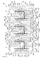
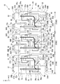
- FIG. 3 is a plan configuration diagram illustrating an example of a semiconductor device according to the present embodiment. It is a perspective view showing an example of a semiconductor device according to the present embodiment.
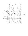
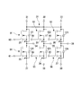
- FIG. 4 is an example of a circuit diagram in the semiconductor device according to the present embodiment. It is a plane block diagram which shows the other example of the semiconductor device by this embodiment. It is another example of the circuit diagram in the semiconductor device by this embodiment. It is a perspective view which shows an example of the lead frame by this embodiment.
- the semiconductor device 10 of the present embodiment includes a first main surface 20a and a second main surface 20b facing each other, and a short direction Y of the first main surface 20a (the vertical direction in FIG. 1). ) And a plurality of terminal plates (power supply terminal plates (leads) 31, 32, 33) extending from the first side surface 20 c of the device main body 20. , And ground terminal plates (leads) 37, 38, 39) and a plurality of terminal plates (output terminal plates (leads) 34, 35, 36, and gate terminal plates (leads) extending from the second side surface 20d of the apparatus body 20). ) 61-66).
- the apparatus main body 20 is formed by integrating apparatus units 21, 22, and 23 corresponding to the plurality of circuit units 41, 42, and 43, respectively.
- the circuit units 41, 42, and 43 are arranged in this order along the longitudinal direction X (the left-right direction in FIG. 1) of the apparatus body 20.
- the device units 21, 22, and 23 include a plurality of wiring boards (power supply wiring board 24, ground wiring boards 25, 26, 27, output wiring boards 28, 29, 30, gate wiring boards 81- 86) and semiconductor elements 91 to 96 disposed on the first main surface of some of the wiring boards and electrically connected to the wiring boards.
- wiring boards power supply wiring board 24, ground wiring boards 25, 26, 27, output wiring boards 28, 29, 30, gate wiring boards 81- 86
- semiconductor elements 91 to 96 disposed on the first main surface of some of the wiring boards and electrically connected to the wiring boards.
- the semiconductor device 10 further includes a sealing resin 50 that covers the device units 21, 22, and 23.
- the first circuit unit 41 includes a first device unit 21, a first power terminal plate 31 and a first ground terminal plate 37 protruding from the first side surface 20 c of the first device unit 21, and a second of the first device unit 21.
- a first output terminal plate 34 protruding from the side surface 20d.
- the second circuit unit 42 includes a second device unit 22, a second power terminal plate 32 and a second ground terminal plate 38 that protrude from the first side surface 20 c of the second device unit 22, and a second device unit 22.
- a second output terminal plate 35 protruding from the side surface 20d.
- the third circuit unit 43 includes a third device unit 23, a third power terminal plate 33 and a third ground terminal plate 39 protruding from the first side surface 20 c of the third device unit 23, and a second device unit 23. And a third output terminal plate 36 protruding from the side surface 20d.
- the first circuit unit 41, the second circuit unit 42, and the third circuit unit 43 have substantially the same shape when viewed in plan.
- the first device unit 21 includes a unit of the power wiring board 24, a first ground wiring board 25, a first output wiring board 28, a first semiconductor element 91, and a fourth semiconductor element 94.
- the second device unit 22 includes a unit of the power supply wiring board 24, a second ground wiring board 26, a second output wiring board 29, a second semiconductor element 92, and a fifth semiconductor element 95.
- the third device unit 23 includes a unit of the power wiring board 24, a third ground wiring board 27, a third output wiring board 30, a third semiconductor element 93, and a sixth semiconductor element 96.
- the sealing resin 50 is provided so that the second main surfaces of the power wiring board 24, the ground wiring boards 25, 26, and 27 and the output wiring boards 28, 29, and 30 are exposed. 27 and output wiring boards 28, 29 and 30, semiconductor elements 91 to 96, power supply terminal boards 31, 32 and 33, output terminal boards 34, 35 and 36, and ground terminal boards 37, 38 and 39 are sealed. ing.
- the sealing resin 50 includes the second main surface 24 b of the power wiring board 24, the second main surfaces 25 b, 26 b, 27 b of the ground wiring boards 25, 26, 27 and the output wiring board 28, Power supply wiring board 24, ground wiring boards 25, 26 and 27, output wiring boards 28, 29 and 30, semiconductor elements 91 to 96, and so as to expose second main surfaces 28b, 29b and 30b of 29 and 30;
- the power supply terminal plates 31, 32, 33, the output terminal plates 34, 35, 36 and the ground terminal plates 37, 38, 39 are sealed.
- the surface (lower surface) 50a exposed to the second main surface side of the sealing resin 50 is arranged on the same surface.
- the second main surface 24b of the power supply wiring board 24, the second main surfaces 25b, 26b, 27b of the ground wiring boards 25, 26, 27 and the second main surfaces 28b, 29b, 30b of the output wiring boards 28, 29, 30 are The lower surface of the apparatus main body 20 is configured.
- the power supply terminal plates 31, 32, 33, the output terminal plates 34, 35, 36 and the ground terminal plates 37, 38, 39 protrude from the sealing resin 50.
- the output terminal plates 34, 35, 36 and the ground terminal plates 37, 38, 39 are perpendicular to the side surfaces from the side surfaces (side surfaces of the sealing resin 50) along the longitudinal direction X of the apparatus main body 20 and opposite to each other. Protruding. Specifically, the ground terminal plates 37, 38, 39 protrude from the first side surface 20 c of the apparatus main body 20 perpendicularly to the side surfaces, whereas the output terminal plates 34, 35, 36 are the second side of the apparatus main body 20. It protrudes perpendicularly to the side surface from the side surface 20d.
- the power supply terminal plates 31, 32, 33 protrude in the same direction as the ground terminal plates 37, 38, 39. Specifically, the power terminal plates 31, 32, 33 and the ground terminal plates 37, 38, 39 all protrude from the first side surface 20 c of the apparatus body 20 perpendicularly to the side surfaces.
- the power supply terminal plates 31, 32, 33 are arranged in a direction (longitudinal direction of the device main body 20) perpendicular to the arrangement direction of the output terminal plates 34, 35, 36 and the ground terminal plates 37, 38, 39 (short direction Y of the device main body 20). It is displaced in the direction X).
- the arrangement direction of the output terminal plates 34, 35, 36 and the ground terminal plates 37, 38, 39 is a direction from the first output terminal plate 34 toward the first ground terminal plate 37, The direction from the second output terminal plate 35 to the second ground terminal plate 38 and the direction from the third output terminal plate 36 to the third ground terminal plate 39.
- the circuit units 41, 42, and 43 may include gate terminal plates 61 to 66 protruding from the second side surface 20d of the device main body 20 (device units 21, 22, and 23).
- the power supply terminal plates 31, 32, 33 and the gate terminal plates 61 to 66 protrude from the side surface along the longitudinal direction X of the apparatus main body 20 in the opposite directions perpendicular to the side surface.
- the power terminal plates 31, 32, and 33 protrude from the first side surface 20 c of the apparatus main body 20 perpendicularly to the side surfaces, whereas the gate terminal plates 61 to 66 have the second side surface 20 d of the apparatus main body 20. Projecting perpendicular to its side.
- the gate terminal plates 61 to 66 protrude from the sealing resin 50.
- the widths of the power supply terminal plates 31, 32, 33, the output terminal plates 34, 35, 36 and the ground terminal plates 37, 38, 39 are larger than the widths of the gate terminal plates 61-66. It is preferable.
- a plurality of terminal boards (power supply terminal boards 31, 32, 33, output terminal boards 34, 35, 36, ground terminal boards 37, 38, 39, and gate terminal boards 61-66) are bent in the middle in the longitudinal direction. It has been.
- the distal end portions (31B to 39B, 61B to 66B) of each terminal plate in the longitudinal direction extend substantially perpendicular to the base end portions (31A to 39A, 61A to 66A).
- the longitudinal end portions (31B to 39B, 61B to 66B) of the terminal boards extending from the plurality of wiring boards are the second main surfaces of the terminal boards (the second main surface 24b of the power supply wiring board 24, the ground).
- the second main surfaces 25b, 26b, 27b of the wiring boards 25, 26, 27 and the second main surfaces 28b, 29b, 30b) of the output wiring boards 28, 29, 30 extend in the opposite direction.
- the tip of each terminal board extending from the plurality of wiring boards extends in the thickness direction of the wiring board so as to protrude from the first main surface of the wiring board (for example, the first main surface 24a of the power supply wiring board 24).
- the apparatus body 20 includes a power supply wiring board 24 common to the three apparatus units 21, 22, 23, ground wiring boards 25, 26, 27 provided individually in the apparatus units 21, 22, and 23, and an apparatus unit 21. , 22 and 23, respectively, output wiring boards 28, 29 and 30 provided individually.
- the power supply wiring board 24, the ground wiring boards 25, 26, and 27 and the output wiring boards 28, 29, and 30 are arranged with a space therebetween.
- the power wiring board 24 extends in the longitudinal direction X of the apparatus main body 20.
- the power supply wiring board 24 has a plurality of narrow portions 24A and wide portions 24B that are alternately connected along the longitudinal direction X of the apparatus body 20, thereby providing a periodic uneven shape in the longitudinal direction X. have.
- the power supply wiring board 24 is in a direction (longitudinal direction of the apparatus main body 20) orthogonal to the arrangement direction of the output terminal boards 34, 35, 36 and the ground terminal boards 37, 38, 39 (short direction Y of the apparatus main body 20).
- X has three narrow portions 24A and three wide portions 24B.
- the narrow portion 24A of the power supply wiring board 24 is narrower than the wide portion 24B in the arrangement direction of the output terminal plates 34, 35, 36 and the ground terminal plates 37, 38, 39 (short direction Y of the apparatus body 20). .
- the wide portion 24B of the power supply wiring board 24 is wider than the narrow portion 24A in the arrangement direction of the output terminal plates 34, 35, 36 and the ground terminal plates 37, 38, 39 (short direction Y of the apparatus body 20). wide.
- the wide portion 24B of the power supply wiring board 24 is connected to one side of the narrow portion 24A (in the short direction Y of the apparatus main body 20) in the arrangement direction of the output terminal plates 34, 35, 36 and the ground terminal plates 37, 38, 39 (short direction Y of the apparatus body 20). It protrudes upward in FIG. Specifically, in the short direction Y of the apparatus main body 20, the wide portion 24B of the power supply wiring board 24 protrudes toward the first side face 20c of the apparatus main body 20 with respect to the narrow portion 24A.
- the power wiring board 24 extends over the entire three circuit units 41, 42, 43.
- the three power terminal plates 31, 32, and 33 are integrally connected to the wide portions 24B of the power wiring board 24, respectively, and project from the wide portions 24B to the first side surface 20c of the apparatus main body 20 in plan view. . That is, the three power terminal boards 31, 32, 33 and the power wiring board 24 are integrally formed.
- the ground wiring boards 25, 26, and 27 are disposed adjacent to the narrow portion 24 ⁇ / b> A of the power wiring board 24 on the first side surface 20 c side where the wide part 24 ⁇ / b> B projects from the power wiring board 24.
- the ground wiring boards 25, 26, and 27 are the two wide portions 24 ⁇ / b> B of the power supply wiring board 24 adjacent to each other in the longitudinal direction X of the apparatus main body 20 and the power supply wiring that connects the two wide portions 24 ⁇ / b> B.
- One plate 24 is arranged in a region surrounded by one narrow portion 24A.
- the ground terminal plates 37, 38, and 39 are integrally connected to the ground wiring boards 25, 26, and 27, respectively, and project from the ground wiring boards 25, 26, and 27 toward the first side surface 20c of the apparatus main body 20 in plan view. ing. That is, the ground terminals 37, 38, 39 and the ground wiring boards 25, 26, 27 are integrally formed.
- the output wiring boards 28, 29, and 30 are arranged on the second side face 20d side opposite to the first side face 20c of the apparatus main body 20 from which the wide portion 24B protrudes in the power wiring board 24.
- the output wiring boards 28, 29, and 30 are arranged in the longitudinal direction X of the apparatus main body 20 along the power wiring board 24, and the number thereof is the number of sets of the narrow part 24A and the wide part 24B of the power wiring board 24, that is, the number of sets. It is equal to the number of circuit units of the device body 20 (the number of device units of the semiconductor device 10).
- each output wiring board of the output wiring boards 28, 29, 30 has narrow portions 28 A, 29 A, 30 A and wide portions 28 B, 29 B, 30 B connected in the longitudinal direction X of the apparatus main body 20.
- the output wiring boards 28, 29, and 30 are arranged in the direction of arrangement of the output terminal boards 34, 35, and 36 and the ground terminal boards 37, 38, and 39 (the short direction Y of the apparatus main body 20). ), And narrow portions 28A, 29A, 30A and wide portions 28B, 29B, 30B, which are continuous in a direction (longitudinal direction X of the apparatus main body 20).
- the narrow portions 28A, 29A, 30A of the output wiring boards 28, 29, 30 are arranged in the arrangement direction of the output terminal boards 34, 35, 36 and the ground terminal boards 37, 38, 39 (short direction Y of the apparatus main body 20).
- the width is narrower than the wide portions 28B, 29B, 30B.
- the wide portions 28B, 29B, 30B of the output wiring boards 28, 29, 30 are arranged in the arrangement direction of the output terminal boards 34, 35, 36 and the ground terminal boards 37, 38, 39 (short direction Y of the apparatus main body 20).
- the width is wider than the narrow portions 28A, 29A, 30A.
- the wide portions 28B, 29B, 30B of the output wiring boards 28, 29, 30 are arranged in the arrangement direction of the output terminal boards 34, 35, 36 and the ground terminal boards 37, 38, 39 (short direction Y of the apparatus main body 20). It protrudes to one side (the lower side in FIG. 1) of the narrow portions 28A, 29A, 30A. That is, the wide portion of each output wiring board protrudes toward the second side surface 20b of the apparatus body 20 with respect to the narrow portion.
- the output terminal plates 34, 35, and 36 are integrally connected to the wide portions 28B, 29B, and 30B of the output wiring boards 28, 29, and 30, respectively, and from the wide portions 28B, 29B, and 30B in a plan view, It protrudes toward the second side surface 20b. That is, the output terminal boards 34, 35, 36 and the output wiring boards 28, 29, 30 are integrally formed.
- the output wiring boards 28, 29, and 30 are arranged in the narrow part (28) of one output wiring board (28) for any two output wiring boards (for example, 28 and 29) adjacent to each other in the longitudinal direction X of the apparatus body 20.
- 28A) faces the wide portion (29B) of the other output wiring board (29).
- the narrow portion (for example, 28A) and the wide portion (28B) of each output wiring board are connected to the pair of the wide portion 24B and the width of the power wiring board 24.
- the narrow portions 24A face each other.
- each output wiring board (for example, 28) is smaller than the total width of each of the narrow portion 24A and the wide portion 24B of the power supply wiring board 24.
- the ground wiring boards 25, 26, 27 are connected to the wide parts 28 B, 29 B, 30 B of the output wiring boards 28, 29, 30 via the narrow part 24 A of the power supply wiring board 24 in the short direction Y of the apparatus body 20. They are arranged to face each other.
- the narrow portion 24A and the wide portion 24B of the power supply wiring board 24 face the wide and narrow portions of the output wiring boards of the output wiring boards 28, 29, and 30 in the short direction Y of the apparatus main body 20, respectively. Is arranged.
- the device main body 20 includes the gate wiring plates 81 to 66 provided for the gate terminal plates 61 to 66 in the device units 21, 22, and 23, respectively. 86.
- the gate wiring boards 81 to 86 are a plurality of first gate wiring boards 82, 84, 84 arranged one by one between two output wiring boards (for example, 28 and 29) adjacent to each other in the longitudinal direction X of the apparatus body 20. 86, each first gate wiring board (for example, 82), a narrow part (28A) of one output wiring board (28) adjacent to the first gate wiring board (82), and a wide part connected thereto. (28B) and a plurality of second gate wiring boards 81, 83, 85 arranged one by one in the region surrounded by.
- the gate terminal plates 61 to 66 are integrally connected to the gate wiring boards 81 to 86, respectively, and project from the gate wiring boards 81 to 86 to the second side face 20d side of the apparatus body 20 in plan view.
- the second gate wiring board 81 is disposed adjacent to the narrow portion 28 ⁇ / b> A of the first output wiring board 28.
- the first gate wiring board 82 is disposed between the first output wiring board 28 and the second output wiring board 29.
- the first circuit unit 41 includes a pair of narrow portions 24A and wide portions 24B of the power supply wiring board 24, one output wiring board 28, one ground wiring board 25, and one first gate wiring.
- a plate 82 and one second gate wiring board 81 are included.
- the second gate wiring board 83 is disposed adjacent to the narrow portion 29 ⁇ / b> A of the second output wiring board 29.
- the first gate wiring board 84 is disposed between the second output wiring board 29 and the third output wiring board 30.
- the second circuit unit 42 includes a pair of the narrow portion 24A and the wide portion 24B of the power supply wiring board 24, one output wiring board 29, one ground wiring board 26, and one first gate wiring.
- a plate 84 and one second gate wiring board 83 are included.
- the second gate wiring board 85 is disposed adjacent to the narrow portion 30 ⁇ / b> A of the third output wiring board 30.
- the first gate wiring board 86 is arranged along the arrangement direction of the third output terminal board 36 and the third ground terminal board 39 (short direction Y of the apparatus body 20) in the third output wiring board 30. Yes.
- the third circuit unit 43 includes a pair of the narrow portion 24A and the wide portion 24B of the power supply wiring board 24, one output wiring board 30, one ground wiring board 27, and one first gate wiring.
- a plate 86 and one second gate wiring board 85 are included.
- the base end portions 31A, 32A, 33A in the extending direction of the power supply terminal plates 31, 32, 33 are formed wider than the other portions (tip portions 31B, 32B, 33B) of the power supply terminal plates 31, 32, 33. ing.
- Steps are preferably provided between the base end portions 31A, 32A, 33A of the power supply terminal plates 31, 32, 33 and the distal end portions 31B, 32B, 33B of the power supply terminal plates 31, 32, 33.
- the base end portions 34A, 35A, 36A in the extending direction of the output terminal plates 34, 35, 36 are formed wider than the other portions (tip portions 34B, 35B, 36B) of the output terminal plates 34, 35, 36. ing.
- a step is provided between the base end portions 34A, 35A, 36A of the output terminal plates 34, 35, 36 and the tip portions 34B, 35B, 36B of the output terminal plates 34, 35, 36.
- the base end portions 37A, 38A, 39A in the extending direction of the ground terminal plates 37, 38, 39 are formed wider than the other portions (tip portions 37B, 38B, 39B) of the ground terminal plates 37, 38, 39. ing.
- a step is provided between the base end portions 37A, 38A, 39A of the ground terminal plates 37, 38, 39 and the front end portions 37B, 38B, 39B of the ground terminal plates 37, 38, 39.
- the base end portions 61A to 66A in the extending direction of the gate terminal plates 61 to 66 are formed wider than the other portions (tip portions 61B to 66B) of the gate terminal plates 61 to 66.
- the width dimension of the base end portions 61A to 66A may be equal to that of the distal end portions 61B to 66B.
- the base end portions 61A to 66A are wider than the front end portions 61B to 66B, the base end portions 61A to 66A of the gate terminal plates 61 to 66 and the front end portions 61B to 66B of the gate terminal plates 61 to 66 are interposed. Is preferably provided with a step.
- the steps between the base end portions (31A to 39A, 61A to 66A) of each terminal plate and the tip portions (31B to 39B, 61B to 66B) are such that the width dimension of each terminal plate is the base end portion (31A to 39A, 61A to 66A) and a shape that changes abruptly at the boundary between the tip portions (31B to 39B, 61B to 66B).
- a step is provided between the base end portion (31A to 39A, 61A to 66A) and the tip end portion (31B to 39B, 61B to 66B) of each terminal plate, so that the tip end portion of each terminal plate is provided.
- Both ends in the width direction of (31B to 39B, 61B to 66B) are located inside the both ends in the width direction of the base end portions (31A to 39A, 61A to 66A) of each terminal board.
- the lower main surfaces 61b to 66b of 61A to 66A, the second main surface (lower surface) 24b of the power supply wiring board 24, the second main surfaces (lower surfaces) 25b, 26b and 27b of the ground wiring boards 25, 26 and 27 and the output wiring board 28. 29, 30 are arranged on the same plane with the second main surfaces (lower surfaces) 28b, 29b, 30b.
- the semiconductor elements 91 to 96 are arranged one by one in each wide part 24B of the power supply wiring board 24 and in each wide part 28B to 30B of the output wiring boards 28-30.
- the semiconductor element 91 is formed on the first main surface 24a of the power wiring board 24 in the vicinity of the base end portions 31A, 32A, 33A (the wide portion 24B) of the power terminal plates 31, 32, 33. , 92, 93 are mounted.
- These semiconductor elements 91, 92, 93 are electrically connected to the narrow portions 28A, 29A, 30A of the output wiring boards 28, 29, 30 through the connectors 101, 102, 103, respectively.
- the semiconductor elements 91, 92, 93 are electrically connected to the first gate wiring boards 82, 84, 86 via connectors 104, 105, 106, respectively.
- the first main surfaces 28a, 29a, and 30a of the portions in the vicinity of the base end portions 34A, 35A, and 36A of the output terminal plates 34, 35, and 36.
- These semiconductor elements 94, 95, and 96 are electrically connected to the ground wiring boards 25, 26, and 27 through connectors 107, 108, and 109, respectively.
- the semiconductor elements 94, 95, and 96 are electrically connected to the second gate wiring boards 81, 83, and 85 through connectors 110, 111, and 112, respectively.
- bonding wires are used as the connectors 101, 102, 103, 107, 108, 109. Further, bonding wires are used as the connectors 104, 105, 106, 110, 111, and 112.
- the first power terminal plate 31, the power wiring board 24, the first semiconductor element 91, the first connector 101, the first output wiring board 28, and the first output terminal board 34 are connected to the first current path. 71 is formed.
- the connector 104 is arranged so as to warp from the first current path 71 as it goes from the first semiconductor element 91 to the first gate wiring board 82.
- the second power terminal plate 32, the power wiring board 24, the second semiconductor element 92, the second connector 102, the second output wiring board 29, and the second output terminal board 35 are connected to the first current path.
- 73 is formed.
- the connector 105 is arranged so as to warp from the first current path 73 as it goes from the second semiconductor element 92 to the first gate wiring board 84.
- the third power terminal plate 33, the power wiring board 24, the third semiconductor element 93, the third connector 103, the third output wiring board 30, and the third output terminal board 36 are connected to the first current path 75. Is forming.
- the connector 106 is arranged so as to warp from the first current path 75 as it goes from the third semiconductor element 93 to the first gate wiring board 86.
- the first output terminal board 34, the first output wiring board 28, the fourth semiconductor element 94, the fourth connector 107, the first ground wiring board 25, and the first ground terminal board 37 are the second one.
- a current path 72 is formed.
- the connector 110 is arranged so as to warp from the second current path 72 as it goes from the fourth semiconductor element 94 to the second gate wiring board 81.
- the second output terminal board 35, the second output wiring board 29, the fifth semiconductor element 95, the fifth connector 108, the second ground wiring board 26, and the second ground terminal board 38 are the second A current path 74 is formed.
- the connector 111 is arranged so as to warp from the second current path 74 as it goes from the fifth semiconductor element 95 to the second gate wiring board 83.
- the third output terminal plate 36, the third output wiring board 30, the sixth semiconductor element 96, the sixth connector 109, the third ground wiring board 27, and the third ground terminal board 39 are provided in the second circuit unit 43.
- a current path 76 is formed.
- the connector 112 is arranged so as to warp from the second current path 76 as it goes from the sixth semiconductor element 96 to the second gate wiring board 85.
- the semiconductor elements 91, 92, 93 disposed in the three wide portions 24B of the power supply wiring board 24 are arranged in the direction in which the output terminal plates 34, 35, 36 and the ground terminal plates 37, 38, 39 are arranged (the short of the device body 20).
- the first element group is configured with an interval in a direction orthogonal to the hand direction Y) (longitudinal direction X of the apparatus main body 20).
- the semiconductor elements 94, 95, and 96 disposed in the wide portions 28B, 29B, and 30B of the three output wiring boards 28, 29, and 30, respectively, are output terminal boards 34, 35, and 36, and ground terminal boards 37, 38,
- the second element group is configured with an interval in a direction (longitudinal direction X of the apparatus main body 20) orthogonal to 39 arrangement directions (short direction Y of the apparatus main body 20).
- a direction in which the center of the fifth semiconductor element 95 constituting the second element group is orthogonal to the arrangement direction of the output terminal plates 34, 35, 36 and the ground terminal plates 37, 38, 39 (short direction Y of the apparatus body 20). It is located between the centers of the first semiconductor element 91 and the second semiconductor element 92 constituting the first element group in the (longitudinal direction X of the apparatus body 20).
- the center of the sixth semiconductor element 96 constituting the second element group is orthogonal to the arrangement direction of the output terminal plates 34, 35, 36 and the ground terminal plates 37, 38, 39 (short direction Y of the apparatus main body 20).
- the second semiconductor element 92 and the third semiconductor element 93 constituting the first element group are located between the centers.
- the sealing resin 50 is provided on the second main surface of the power wiring board 24, the output wiring boards 28, 29, and 30 and the ground wiring boards 25, 26, and 27 (the surface opposite to the first main surface, that is, the apparatus main body 20).
- the power supply wiring board 24, the output wiring boards 28, 29, and 30 and the ground wiring boards 25, 26, and 27 are sealed so that the lower surface 20b) is exposed.
- the sealing resin 50 has through holes 51, 51 penetrating in the thickness direction of the power wiring board 24, the output wiring boards 28, 29, 30 and the ground wiring boards 25, 26, 27. May be formed.
- the through holes 51, 51 of the sealing resin 50 are arranged in the direction in which the output terminal plates 34, 35, 36 and the ground terminal plates 37, 38, 39 are arranged in the sealing resin 50 (short of the device main body 20 It is preferably formed at both ends in a direction (longitudinal direction X of the apparatus main body 20) orthogonal to the hand direction Y).
- the materials of the plates 37, 38, 39 and the gate terminal plates 61 to 66 are not particularly limited, but may be materials used for general lead frames such as copper.
- the sealing resin 50 is not particularly limited, but may be a material generally used for sealing a semiconductor device, for example.
- a circuit diagram of the semiconductor device 10 of the present embodiment is, for example, as shown in FIG.
- the first semiconductor element 91, the second semiconductor element 92, the third semiconductor element 93, the fourth semiconductor element 94, the fifth semiconductor element 95, and the sixth semiconductor element 96 include the drain electrode and the source.
- the semiconductor device 10 of this embodiment can be used for operation control of a motor (for example, a three-phase motor).
- the power supply terminal plates 31, 32, and 33 are connected to a DC power supply (not shown).
- a direct current flows through the power supply terminal plates 31, 32, 33 and a gate signal is intermittently applied to the gate electrodes of the semiconductor elements 91, 92, 93 as switching elements, the first current paths 71, 73, In 75, a direct current flows intermittently from the power supply terminal plates 31, 32, 33 toward the output terminal plates 34, 35, 36.
- the semiconductor device 10 including the three circuit units 41, 42, and 43 is illustrated, but the present embodiment is not limited to this.
- the semiconductor device of the present embodiment only needs to include at least one circuit unit.
- the connectors 101, 102, 103, 107, 108, and 109 are illustrated, but the present embodiment is not limited to this.
- the connectors 101, 102, 103, 107, 108, and 109 of the connectors in the present embodiment may be conductive plate materials.
- the power wiring board 24 and the output wiring boards 28, 29, and 30 are connected by the first capacitors 121, 122, and 123, and the output wiring boards 28, 29, and 30 and the ground wiring boards 25, 26, and 27 may be connected by second capacitors 124, 125, and 126. That is, the circuit units 41, 42, and 43 of this embodiment may include the capacitors 121 to 126.
- the first capacitors 121 to 123 are connected in parallel with the semiconductor elements 91 to 93 between the power supply wiring board 24 and the output wiring boards 28 to 30.
- the second capacitors 124 to 126 are connected in parallel with the semiconductor elements 94 to 96 between the output wiring boards 28, 29, 30 and the ground wiring boards 25, 26, 27.
- the semiconductor device 10 includes the device main body 20, one power supply wiring board 24, a plurality of output wiring boards 28 to 30, and a plurality of semiconductor elements 91 to 96.
- the apparatus main body 20 has a first main surface 20a and a second main surface 20b that face each other, and a first side surface 20c and a second side surface 20d that face each other in the lateral direction Y of the first main surface 20a.
- One power supply wiring board 24 has a plurality of sets of narrow portions 24A and wide portions 24B alternately connected in the longitudinal direction X of the first major surface 20a, and the wide portion 24B is the narrow portion 24A in the short direction Y. It protrudes toward the first side surface 20c.
- the plurality of output wiring boards 28 to 30 are arranged in the longitudinal direction X along the power supply wiring board 24.
- the number of the plurality of output wiring boards 28 to 30 is equal to the number of the narrow portions 24A and the wide portions 24B of the power wiring board 24.
- Each output wiring board of the plurality of output wiring boards 28 to 30 has a narrow part 28A and a wide part 28B connected in the longitudinal direction X, and the wide part 28B is closer to the second side face 20d than the narrow part 28A. It protrudes.
- the plurality of semiconductor elements 91 to 96 are arranged one by one in each wide portion 24B of the power supply wiring board 24 and in each wide portion 28B to 30B of the output wiring boards 28-30.
- the narrow portion (28A) of one output wiring board (28) is connected to the other output wiring board (29). It faces the wide part (29B).
- the narrow portion (28A) and the wide portion (28B) of each output wiring board face the pair of the wide portion 24B and the narrow portion 24A of the power wiring board 24, respectively.
- the width of each output wiring board (for example, 28) is smaller than the sum of the widths of the pair of narrow portions 24A and wide portions 24B of the power wiring board 24.
- the power supply wiring is also provided between two output wiring boards (for example, 28 and 29) adjacent to each other in the longitudinal direction X and between the narrow portion of each output wiring board and the second side surface 20d of the apparatus main body 20. A region for providing a wiring board other than the board and the output wiring board can be secured.
- the ground wiring board, the first gate wiring board, and the second gate wiring board described above can be arranged in these regions while ensuring the pitch between the terminal boards to be connected to each wiring board. Therefore, if these wiring boards are arranged, the heat radiation area can be increased while ensuring the pitch between the adjacent terminal boards.
- the area secured in this way is the case where the power supply wiring board 24 and each output wiring board are arranged to engage with each other, that is, the wide portion 24B of the power supply wiring board 24 is the first part of the apparatus main body 20.
- the wide portion of each output wiring board projects to the first side surface 20c side instead of the second side surface 20d side of the device main body 20. This is an area that cannot be secured.
- the semiconductor device 10 includes two wide portions 24B of the power supply wiring board 24 adjacent to each other in the longitudinal direction X and one width of the power supply wiring board 24 that connects the two wide portions 24B. It further includes a plurality of ground wiring boards 25 to 27 arranged one by one in a region surrounded by the narrow portion 24A. Each ground wiring board (for example, 25) of the plurality of ground wiring boards 25 to 27 faces the wide part 28B of one output wiring board 28 via one narrow part 24A of the power wiring board 24 in the short direction Y. ing.
- the heat dissipation area can be increased while securing the pitch between adjacent terminal boards, and the semiconductor device can be further compacted.
- the semiconductor device 10 includes a plurality of first gate wiring boards 82 arranged one by one between two output wiring boards (for example, 28 and 29) adjacent to each other in the longitudinal direction X. 84, 86, each first gate wiring board (for example, 82) of the plurality of first gate wiring boards 82, 84, 86, and one output wiring board (28) adjacent to the first gate wiring board (82).
- the heat dissipation area can be increased while securing the pitch between adjacent terminal boards, and the semiconductor device can be further compacted.
- the apparatus main body 20 is composed of a plurality of circuit units 41, 42, 43, and each circuit unit (for example, 41) of the plurality of circuit units 41, 42, 43 is connected to a power wiring board ( 24) a pair of narrow portion (24A) and wide portion (24B), one output wiring board (28), one ground wiring board (25), and one first gate wiring board (82). And one second gate wiring board (81).
- the heat dissipation area can be increased while securing the pitch between adjacent terminal boards, and the semiconductor device can be further compacted.
- each circuit unit has the same structure, the manufacturing process of the semiconductor device 10 can be simplified. More specifically, since the shape and arrangement of each wiring board and each semiconductor element are the same among the circuit units, the wide portions 24B of the power supply wiring board 24 and the wide portions 28B to 28B of the output wiring boards 28 to 30 are used. In the process of mounting the semiconductor elements 91 to 96 one by one on 30B, it is not necessary to position the semiconductor elements for each circuit unit.
- the semiconductor device 10 includes the first semiconductor element (91) arranged in the wide portion 24B of the power supply wiring board 24 and one output wiring board (28) in each circuit unit (for example, 41). ) Of the first connector (101) for electrical connection with the narrow portion (28A), the second semiconductor element (94) disposed in the wide portion (28B) of one output wiring board (28), and one A second connector (107) that electrically connects the ground wiring board (25), and a third connector (104) that electrically connects the first semiconductor element (91) and one first gate wiring board (82). And a fourth connector (110) for electrically connecting the second semiconductor element (94) and one second gate wiring board (81).
- the heat dissipation area can be increased, and further downsizing of the semiconductor device can be achieved.
- each circuit unit has the same structure, the manufacturing process of the semiconductor device 10 can be simplified. More specifically, since the shape and arrangement of each wiring board and each semiconductor element are the same between each circuit unit, the step of electrically connecting the first semiconductor element and the first gate wiring board with the first connector, In the step of electrically connecting the two semiconductor elements and the second gate wiring board with the second connector, the electrical connection can be made with high accuracy without rotating the apparatus body 20.
- the semiconductor device 10 is integrally connected to each of the wide portions 24B of the power supply wiring board 24, and from each of the wide portions 24B to the first side surface 20c side of the device body 20 in plan view.
- the plurality of power supply terminal boards 31 to 33 and the plurality of ground wiring boards 25 to 27 are integrally connected to each other, and from the plurality of ground wiring boards 25 to 27 on the first side face 20c side of the apparatus body 20 in plan view.
- the plurality of ground terminal plates 37 to 39 projecting to the wide width portions 28B to 30B of the plurality of output wiring boards 28 to 30, respectively, are integrally connected to each other, and from the wide portions 28B to 30B in plan view,
- the plurality of output terminal boards 34 to 36 projecting to the second side face 20d side and the plurality of first gate wiring boards 82, 84, 86 are integrally connected to each other, and the second side face 20d side of the apparatus body 20 in plan view.
- What The plurality of first gate terminal plates 62, 64, 66 to be brought out and the plurality of second gate wiring boards 81, 83, 85 are integrally connected to the second side surface 20d side of the apparatus body 20 in plan view.
- the plurality of power supply terminal plates 31 to 33 and the plurality of output terminal plates 34 to 36 are longer in the longitudinal direction X than the plurality of first gate terminal plates 62, 64, 66 and the plurality of second gate terminal plates 61, 63, 65.
- the width is large.
- the heat dissipation area can be increased while securing the pitch between adjacent terminal boards, and the semiconductor device can be further compacted.
- the 3rd connector (104) goes to one 1st gate wiring board (82) from the 1st semiconductor element (91), From one power supply terminal board (31) to one output terminal board (34) through the power supply wiring board 24, the first semiconductor element (91), the first connector (101), and one output wiring board (28). ) To be warped from the first current path (71) leading to).
- the fourth connector (110) has one first output terminal board (34) as it goes from the second semiconductor element (94) to one second gate wiring board (81). To one ground terminal board (37) through one output wiring board (28), a fourth semiconductor element (94), a fourth connector (107), and one ground wiring board (25). It arrange
- the heat dissipation area can be increased while securing the pitch between adjacent terminal boards, and the semiconductor device can be further compacted.
- a step of connecting the first semiconductor element (91) and the narrow portion (28A) of the output wiring board (28) with the first connector (101), the first semiconductor element (91) and the first gate wiring In the step of connecting the plate (82) with the third connector (104), even if the distance between the first connector (101) and the third connector (104) is short, the first connector (101 ) And the third connector (104) can be avoided more than in the case where the third connector (104) is arranged in parallel with each other. Moreover, compared with the case where the 1st connector (101) and the 3rd connector (104) are arrange
- Have The base end portions 31A to 39A and 61A to 66A of each terminal plate are wider than the other portions 31B to 39B and 61B to 66B of the terminal plates.
- the heat dissipation area can be increased while ensuring the pitch between the adjacent terminal boards. Therefore, heat generated in the semiconductor elements 91 to 96 can be efficiently released to the outside. Furthermore, the semiconductor device can be further downsized.
- each terminal plate power supply terminal plates 31, 32, 33, output terminal plates 34, 35, 36 and ground terminal plates 37, 38, 39, gate terminal plates 61 to 66. Steps are provided between the portions (31A to 39A, 61A to 66A) and the other portions (31B to 39B, 61B to 66B) of the terminal board.
- step difference can be used as the mark of the bending position of a terminal board.
- a plurality of wiring boards (power supply wiring board 24, ground wiring boards 25, 26, 27, output wiring boards 28, 29, 30 and gate wiring boards 81 to 86) are respectively connected to terminal boards (power supply boards).
- Terminal boards 31, 32, 33, output terminal boards 34, 35, 36, ground terminal boards 37, 38, 39, and gate terminal boards 61-66) are integrally formed.
- the semiconductor device 10 can be made compact while suppressing electrical loss in the semiconductor device 10.
- the base end portion of the terminal plate (power supply terminal plates 31, 32, 33, output terminal plates 34, 35, 36 and ground terminal plates 37, 38, 39, gate terminal plates 61 to 66).
- the surfaces 25b, 26b, 27b and the second main surfaces 28b, 29b, 30b) of the output wiring boards 28, 29, 30 are arranged on the same surface.
- semiconductor elements 91 to 96 are arranged on the first main surface of some of the wiring boards.
- the heat generated in the semiconductor elements 91 to 96 can be efficiently released to the outside.
- the plurality of terminal plates include the power supply terminal plates 31, 32, and 33, and the output terminal plates 34, 35, extending from the apparatus main body 20 in the opposite direction to the power supply terminal plates 31, 32, and 33. 36, and ground terminal plates 37, 38, 39 extending from the apparatus main body 20 in the same direction as the power terminal plates 31, 32, 33.
- the plurality of wiring boards include a power wiring board 24 connected to the power terminal boards 31, 32, 33, ground wiring boards 25, 26, 27 connected to the ground terminal boards 37, 38, 39, and an output terminal board. And output wiring boards 28, 29, 30 connected to 34, 35, 36.
- the power wiring board 24 includes a plurality of narrow portions 24A and wide portions 24B that are continuous in a direction orthogonal to the arrangement direction of the output terminal plates 34, 35, and 36 and the ground terminal plates 37, 38, and 39.
- the heat generated in the three semiconductor elements 91, 92, and 93 disposed in the wide portion 24 ⁇ / b> B of the power supply wiring board 24 can be evenly released by the entire power supply wiring board 24. That is, the heat dissipation efficiency can be improved.
- the semiconductor elements 91, 92, 93 disposed on the first main surface 24a of the wide portion 24B of the power wiring board 24 and the narrow portions 28A, 28A, 29, 30 of the output wiring boards 28, 29, 30 are provided.
- 29A, 30A are connected by connectors 101, 102, 103, and semiconductor elements 94 arranged on the first main surfaces 28a, 29a, 30a of the wide portions 28B, 29B, 30B of the output wiring boards 28, 29, 30, 95, 96 and ground wiring boards 25, 26, 27 are connected by connectors 107, 108, 109.
- the heat generated in the semiconductor elements 91, 92, 93 can be efficiently transmitted to the narrow portions 28A, 29A, 30A of the output wiring boards 28, 29, 30 through the connectors 101, 102, 103. Further, the heat generated in the semiconductor elements 94, 95, and 96 can be efficiently transferred to the ground wiring boards 25, 26, and 27 through the connectors 107, 108, and 109. Therefore, the heat dissipation efficiency of the semiconductor device 10 can be improved.
- the connectors 101, 102, 103, 107, 108, 109 are conductive plate materials.
- the plate material has a smaller electrical resistance than the bonding wire, the electrical loss in the semiconductor device 10 can be reduced. Further, since the plate material has a higher thermal conductivity than the bonding wire, the heat dissipation efficiency of the semiconductor device 10 can be further improved.
- the through holes 51 and 51 penetrating in the thickness direction of the power wiring board 24, the output wiring boards 28, 29, and 30 and the ground wiring boards 25, 26, and 27 are formed in the sealing resin 50. ing.
- the semiconductor device 10 can be fixed to the heat dissipation member by screwing using the through holes 51, 51.
- the second main surface (the lower surface of the apparatus main body 20) of the power supply wiring board 24, the output wiring boards 28, 29, and 30 and the ground wiring boards 25, 26, and 27 can be pressed against the heat radiating member.
- the through holes 51 and 51 are formed at both ends of the sealing resin 50 in the direction orthogonal to the arrangement direction of the output terminal plates 34, 35 and 36 and the ground terminal plates 37, 38 and 39.
- the surface contact of the second main surface (the lower surface 20b of the apparatus main body 20) of the power supply wiring board 24, the output wiring boards 28, 29, and 30 and the ground wiring boards 25, 26, and 27 and the heat radiating member can be ensured.
- the heat generated in the semiconductor elements 91 to 96 can be more efficiently released from the second main surface of these wiring boards to the heat radiating member.
- the plurality of terminal boards include the gate terminal boards 61 to 66 extending from the apparatus main body 10 in the direction opposite to the power supply terminal boards 31, 32, 33.
- the semiconductor device is secured while ensuring the space between the power supply terminal plates 31, 32, 33 and the ground terminal plates 37, 38, 39 and the space between the output terminal plates 34, 35, 36 and the gate terminal plates 61-66. 10 can be miniaturized in the longitudinal direction.
- the wiring boards include the gate wiring boards 81, 83, and 85.
- the terminal boards include power terminal boards 31, 32, 33 connected to the power wiring board 24, ground terminal boards 37, 38, 39 connected to the ground wiring boards 25, 26, 27, output wiring boards 28, There are output terminal plates 34, 35, 36 connected to 29, 30 and gate terminal plates 61-66 connected to gate wiring plates 81, 83, 85.
- the widths of the power terminals 31, 32, 33, the output terminal plates 34, 35, 36 and the ground terminal plates 37, 38, 39 are larger than the widths of the gate terminals 61-66.
- the semiconductor device 10 can be made compact while suppressing electrical loss in the semiconductor device 10. Since a large current flows through the power supply terminal boards 31, 32, 33, the output terminal boards 34, 35, 36 and the ground terminal boards 37, 38, 39, by making these terminal boards wide, these terminal boards It is possible to suppress electrical loss in these terminal boards by suppressing the electrical resistance to be small.
- the semiconductor elements 91, 92, 93 disposed in the plurality of wide portions 24 ⁇ / b> B of the power supply wiring board 24 include the output terminal plates 34, 35, 36 and the ground terminal plates 37, 38,
- the first element group is configured with an interval in a direction (longitudinal direction X of the apparatus main body 20) orthogonal to 39 arrangement directions (short direction Y of the apparatus main body 20).
- the semiconductor elements 94, 95, 96 disposed in the wide portions 28B, 29B, 30B of the plurality of output wiring boards 28, 29, 30 are output terminal boards 34, 35, 36 and ground terminal boards 37, 38, 39, respectively.
- the centers of the semiconductor element plates 95, 96 constituting the second element group are orthogonal to the arrangement direction of the output terminal plates 34, 35, 36 and the ground terminal plates 37, 38, 39 (short direction Y of the apparatus main body 20).
- the direction (longitudinal direction X of the apparatus main body 20) it is located between the centers of two of the semiconductor elements 91, 92, 93 constituting the first element group.
- the first current paths 71, 73, 75 and the second current paths 72, 74, 76 can be further simplified. Further, it is possible to equalize the heat distribution in the apparatus main body 20 based on the heat generated in the plurality of semiconductor elements 91 to 96. That is, heat concentration in the device body 20 can be prevented, and the heat dissipation efficiency of the semiconductor device 10 can be improved.
- the power supply wiring board 24, the output wiring boards 28, 29, and 30, the power supply terminals 31, 32, and 33 extending from the ground wiring boards 25, 26, and 27, the output terminals 34, 35, and 36, and the ground.
- the tip portions of the terminals 37, 38, 39 extend in the thickness direction of these wiring boards so as to protrude from the first main surface of these wiring boards.
- the semiconductor device 10 can be connected to a circuit board or the like at a position away from the heat dissipating member with which the lower surface of the semiconductor device 10 contacts.
- the power supply wiring board 24 and the output wiring boards 28, 29, 30 are connected by the capacitors 121, 122, 123, and the output wiring boards 28, 29, 30 and the ground wiring boards 25, 26, 27 is connected by capacitors 124, 125, 126.
- the semiconductor elements 91 to 96 are switching elements such as MOF-FETs or IGBTs mounted on the in-vehicle electrical equipment, currents intermittently flow due to the switching of the semiconductor elements 91 to 96.
- the semiconductor device 10 by providing the capacitors 121 to 126, voltage fluctuations during switching of the semiconductor elements 91 to 96 can be reduced.
- the lead frame 200 of this embodiment includes a plurality of wiring boards (power supply wiring board 24, ground wiring boards 25, 26, 27, output wiring boards 28, 29, 30 and gate wiring boards 81-86. ) And a plurality of terminal boards (power supply terminal boards (leads) 31, 32, 33, output terminal boards (leads) 34, 35, 36, ground terminal boards (leads) 37, 38, 39, gate terminal boards 61-66. ) Are integrally formed, and a plurality of terminal plates are connected by connecting portions (tie bars 201, 202 and frame portion 203).
- the tie bars 201 and 202 among the connecting portions connect the portions in the vicinity of the plurality of wiring boards (base end portions (31A to 39A, 61A to 66A)) of the plurality of terminal boards over the arrangement direction of the plurality of terminal boards. Is formed.
- the frame body portion 203 includes a portion of the plurality of terminal plates opposite to the plurality of wiring boards (tip portions (31B to 39B, 61B to 66B)) and a plurality of terminal plates in the tie bars 201 and 202. It connects with the part to isolate
- the lead frame 200 of this embodiment is used as a lead frame for the semiconductor device 10.
- the lead frame 200 of this embodiment includes a plurality of wiring boards (power supply wiring board 24, ground wiring boards 25, 26, 27, output wiring boards 28, 29, 30, and gate wiring board 81 that constitute the semiconductor device 10. 86), a plurality of terminal boards (power supply terminal boards (leads) 31, 32, 33, output terminal boards (leads) 34, 35, 36, ground terminal boards (leads) 37, 38, 39, gate terminal board 61). To 66).
- the semiconductor device 10 described above can be manufactured using the lead frame 200 of the present embodiment.
Landscapes
- Inverter Devices (AREA)
- Engineering & Computer Science (AREA)
- Lead Frames For Integrated Circuits (AREA)
- Microelectronics & Electronic Packaging (AREA)
- Power Engineering (AREA)
- Structure Of Printed Boards (AREA)
Abstract
Priority Applications (4)
| Application Number | Priority Date | Filing Date | Title |
|---|---|---|---|
| US15/516,825 US10438872B2 (en) | 2016-03-11 | 2016-07-13 | Semiconductor device and lead frame |
| CN201680003463.0A CN107683525B (zh) | 2016-03-11 | 2016-07-13 | 半导体装置以及引线框 |
| JP2016574026A JP6277292B1 (ja) | 2016-03-11 | 2016-07-13 | 半導体装置及びリードフレーム |
| NL2018487A NL2018487B1 (en) | 2016-03-11 | 2017-03-09 | Semiconductor device and lead frame |
Applications Claiming Priority (2)
| Application Number | Priority Date | Filing Date | Title |
|---|---|---|---|
| JPPCT/JP2016/057766 | 2016-03-11 | ||
| PCT/JP2016/057766 WO2017154199A1 (fr) | 2016-03-11 | 2016-03-11 | Dispositif à semi-conducteur et grille de connexion |
Publications (1)
| Publication Number | Publication Date |
|---|---|
| WO2017154232A1 true WO2017154232A1 (fr) | 2017-09-14 |
Family
ID=58670270
Family Applications (2)
| Application Number | Title | Priority Date | Filing Date |
|---|---|---|---|
| PCT/JP2016/057766 Ceased WO2017154199A1 (fr) | 2016-03-11 | 2016-03-11 | Dispositif à semi-conducteur et grille de connexion |
| PCT/JP2016/070664 Ceased WO2017154232A1 (fr) | 2016-03-11 | 2016-07-13 | Dispositif à semi-conducteurs et grille de connexion |
Family Applications Before (1)
| Application Number | Title | Priority Date | Filing Date |
|---|---|---|---|
| PCT/JP2016/057766 Ceased WO2017154199A1 (fr) | 2016-03-11 | 2016-03-11 | Dispositif à semi-conducteur et grille de connexion |
Country Status (5)
| Country | Link |
|---|---|
| US (1) | US10438872B2 (fr) |
| JP (1) | JP6277292B1 (fr) |
| CN (1) | CN107683525B (fr) |
| NL (1) | NL2018487B1 (fr) |
| WO (2) | WO2017154199A1 (fr) |
Cited By (1)
| Publication number | Priority date | Publication date | Assignee | Title |
|---|---|---|---|---|
| JP2020155706A (ja) * | 2019-03-22 | 2020-09-24 | 三菱電機株式会社 | 電力半導体装置及びその製造方法 |
Families Citing this family (3)
| Publication number | Priority date | Publication date | Assignee | Title |
|---|---|---|---|---|
| WO2018109820A1 (fr) | 2016-12-13 | 2018-06-21 | 新電元工業株式会社 | Module électronique |
| NL2020161B1 (en) * | 2017-12-22 | 2019-07-01 | Shindengen Electric Mfg | Electronic module |
| US11183943B2 (en) * | 2018-06-08 | 2021-11-23 | Shindengen Electric Manufacturing Co., Ltd. | Semiconductor module |
Citations (10)
| Publication number | Priority date | Publication date | Assignee | Title |
|---|---|---|---|---|
| JPH0397940U (fr) * | 1990-01-25 | 1991-10-09 | ||
| JPH09275174A (ja) * | 1996-04-05 | 1997-10-21 | Toko Inc | 電子部品 |
| JP2010104204A (ja) * | 2008-10-27 | 2010-05-06 | Denso Corp | 電力変換装置 |
| JP2011238906A (ja) * | 2010-04-14 | 2011-11-24 | Denso Corp | 半導体モジュール |
| WO2012108011A1 (fr) * | 2011-02-09 | 2012-08-16 | 三菱電機株式会社 | Module module semi-conducteur de puissance |
| JP2012182250A (ja) * | 2011-02-28 | 2012-09-20 | Sanken Electric Co Ltd | 半導体装置 |
| JP2012249457A (ja) * | 2011-05-30 | 2012-12-13 | Denso Corp | 半導体モジュール、及び、それを用いた駆動装置 |
| JP2013051376A (ja) * | 2011-08-31 | 2013-03-14 | Denso Corp | 電子装置の製造方法 |
| WO2014174573A1 (fr) * | 2013-04-22 | 2014-10-30 | 三菱電機株式会社 | Dispositif à semi-conducteurs, et procédé de fabrication associé |
| JP2015090960A (ja) * | 2013-11-07 | 2015-05-11 | 株式会社デンソー | 半導体パッケージ |
Family Cites Families (7)
| Publication number | Priority date | Publication date | Assignee | Title |
|---|---|---|---|---|
| JPS5669866A (en) | 1979-11-09 | 1981-06-11 | Fujitsu Ltd | Semiconductor element |
| JPH0397940A (ja) | 1989-09-08 | 1991-04-23 | Klimovsky Spezial Konstr Bjuro Po Proektirov Tkatskogo Oborud | 取りはずし可能なクロスロールを有する織機 |
| JP4459883B2 (ja) * | 2005-04-28 | 2010-04-28 | 三菱電機株式会社 | 半導体装置 |
| JP5285348B2 (ja) * | 2008-07-30 | 2013-09-11 | セミコンダクター・コンポーネンツ・インダストリーズ・リミテッド・ライアビリティ・カンパニー | 回路装置 |
| KR101237566B1 (ko) | 2011-07-20 | 2013-02-26 | 삼성전기주식회사 | 전력 모듈 패키지 및 그 제조방법 |
| WO2013171996A1 (fr) * | 2012-05-16 | 2013-11-21 | パナソニック株式会社 | Module semi-conducteur de puissance |
| CN202749368U (zh) * | 2012-09-12 | 2013-02-20 | 无锡华润矽科微电子有限公司 | 收录机前置功放电路封装结构 |
-
2016
- 2016-03-11 WO PCT/JP2016/057766 patent/WO2017154199A1/fr not_active Ceased
- 2016-07-13 JP JP2016574026A patent/JP6277292B1/ja active Active
- 2016-07-13 CN CN201680003463.0A patent/CN107683525B/zh active Active
- 2016-07-13 WO PCT/JP2016/070664 patent/WO2017154232A1/fr not_active Ceased
- 2016-07-13 US US15/516,825 patent/US10438872B2/en active Active
-
2017
- 2017-03-09 NL NL2018487A patent/NL2018487B1/en active
Patent Citations (10)
| Publication number | Priority date | Publication date | Assignee | Title |
|---|---|---|---|---|
| JPH0397940U (fr) * | 1990-01-25 | 1991-10-09 | ||
| JPH09275174A (ja) * | 1996-04-05 | 1997-10-21 | Toko Inc | 電子部品 |
| JP2010104204A (ja) * | 2008-10-27 | 2010-05-06 | Denso Corp | 電力変換装置 |
| JP2011238906A (ja) * | 2010-04-14 | 2011-11-24 | Denso Corp | 半導体モジュール |
| WO2012108011A1 (fr) * | 2011-02-09 | 2012-08-16 | 三菱電機株式会社 | Module module semi-conducteur de puissance |
| JP2012182250A (ja) * | 2011-02-28 | 2012-09-20 | Sanken Electric Co Ltd | 半導体装置 |
| JP2012249457A (ja) * | 2011-05-30 | 2012-12-13 | Denso Corp | 半導体モジュール、及び、それを用いた駆動装置 |
| JP2013051376A (ja) * | 2011-08-31 | 2013-03-14 | Denso Corp | 電子装置の製造方法 |
| WO2014174573A1 (fr) * | 2013-04-22 | 2014-10-30 | 三菱電機株式会社 | Dispositif à semi-conducteurs, et procédé de fabrication associé |
| JP2015090960A (ja) * | 2013-11-07 | 2015-05-11 | 株式会社デンソー | 半導体パッケージ |
Cited By (4)
| Publication number | Priority date | Publication date | Assignee | Title |
|---|---|---|---|---|
| JP2020155706A (ja) * | 2019-03-22 | 2020-09-24 | 三菱電機株式会社 | 電力半導体装置及びその製造方法 |
| CN111725151A (zh) * | 2019-03-22 | 2020-09-29 | 三菱电机株式会社 | 功率半导体装置及其制造方法 |
| JP7215271B2 (ja) | 2019-03-22 | 2023-01-31 | 三菱電機株式会社 | 電力半導体装置及びその製造方法 |
| US11735509B2 (en) | 2019-03-22 | 2023-08-22 | Mitsubishi Electric Corporation | Power semiconductor device and manufacturing method thereof |
Also Published As
| Publication number | Publication date |
|---|---|
| CN107683525B (zh) | 2020-08-14 |
| WO2017154199A1 (fr) | 2017-09-14 |
| JPWO2017154232A1 (ja) | 2018-03-22 |
| US20180277469A1 (en) | 2018-09-27 |
| CN107683525A (zh) | 2018-02-09 |
| JP6277292B1 (ja) | 2018-02-07 |
| NL2018487A (en) | 2017-09-20 |
| US10438872B2 (en) | 2019-10-08 |
| NL2018487B1 (en) | 2017-11-16 |
Similar Documents
| Publication | Publication Date | Title |
|---|---|---|
| US9795049B2 (en) | Semiconductor device | |
| JP6275292B1 (ja) | 半導体装置及びその製造方法 | |
| CN103314437B (zh) | 功率半导体模块及电源单元装置 | |
| JP6277292B1 (ja) | 半導体装置及びリードフレーム | |
| CN105378922A (zh) | 功率模块 | |
| CN111919295A (zh) | 半导体组件 | |
| KR100773289B1 (ko) | 반도체 장치 | |
| WO2015162712A1 (fr) | Module à semi-conducteurs et convertisseur de puissance faisant appel à celui-ci | |
| JP6236553B1 (ja) | 半導体装置 | |
| JP5544767B2 (ja) | 半導体装置 | |
| JP7218677B2 (ja) | 基板構造体 | |
| CN105612616A (zh) | 半导体模块 | |
| US20210183807A1 (en) | Electronic module | |
| CN115380377A (zh) | 半导体模块 | |
| JP6136657B2 (ja) | 半導体モジュール | |
| JP6325757B1 (ja) | 電子装置 | |
| JP2018133463A (ja) | 半導体モジュール | |
| JP6136656B2 (ja) | 半導体モジュール | |
| JP2015216148A (ja) | パワー半導体モジュール |
Legal Events
| Date | Code | Title | Description |
|---|---|---|---|
| ENP | Entry into the national phase |
Ref document number: 2016574026 Country of ref document: JP Kind code of ref document: A |
|
| WWE | Wipo information: entry into national phase |
Ref document number: 15516825 Country of ref document: US |
|
| NENP | Non-entry into the national phase |
Ref country code: DE |
|
| 121 | Ep: the epo has been informed by wipo that ep was designated in this application |
Ref document number: 16893556 Country of ref document: EP Kind code of ref document: A1 |
|
| 122 | Ep: pct application non-entry in european phase |
Ref document number: 16893556 Country of ref document: EP Kind code of ref document: A1 |