WO2017154355A1 - Procédé de fabrication d'élément de conversion de longueur d'onde, et élément de conversion de longueur d'onde - Google Patents
Procédé de fabrication d'élément de conversion de longueur d'onde, et élément de conversion de longueur d'onde Download PDFInfo
- Publication number
- WO2017154355A1 WO2017154355A1 PCT/JP2017/001449 JP2017001449W WO2017154355A1 WO 2017154355 A1 WO2017154355 A1 WO 2017154355A1 JP 2017001449 W JP2017001449 W JP 2017001449W WO 2017154355 A1 WO2017154355 A1 WO 2017154355A1
- Authority
- WO
- WIPO (PCT)
- Prior art keywords
- container
- wavelength conversion
- conversion member
- side wall
- glass frit
- Prior art date
- Legal status (The legal status is an assumption and is not a legal conclusion. Google has not performed a legal analysis and makes no representation as to the accuracy of the status listed.)
- Ceased
Links
Images






Classifications
-
- C—CHEMISTRY; METALLURGY
- C03—GLASS; MINERAL OR SLAG WOOL
- C03C—CHEMICAL COMPOSITION OF GLASSES, GLAZES OR VITREOUS ENAMELS; SURFACE TREATMENT OF GLASS; SURFACE TREATMENT OF FIBRES OR FILAMENTS MADE FROM GLASS, MINERALS OR SLAGS; JOINING GLASS TO GLASS OR OTHER MATERIALS
- C03C8/00—Enamels; Glazes; Fusion seal compositions being frit compositions having non-frit additions
- C03C8/24—Fusion seal compositions being frit compositions having non-frit additions, i.e. for use as seals between dissimilar materials, e.g. glass and metal; Glass solders
-
- C—CHEMISTRY; METALLURGY
- C03—GLASS; MINERAL OR SLAG WOOL
- C03C—CHEMICAL COMPOSITION OF GLASSES, GLAZES OR VITREOUS ENAMELS; SURFACE TREATMENT OF GLASS; SURFACE TREATMENT OF FIBRES OR FILAMENTS MADE FROM GLASS, MINERALS OR SLAGS; JOINING GLASS TO GLASS OR OTHER MATERIALS
- C03C27/00—Joining pieces of glass to pieces of other inorganic material; Joining glass to glass other than by fusing
- C03C27/06—Joining glass to glass by processes other than fusing
-
- G—PHYSICS
- G02—OPTICS
- G02B—OPTICAL ELEMENTS, SYSTEMS OR APPARATUS
- G02B5/00—Optical elements other than lenses
- G02B5/20—Filters
Definitions
- the present invention relates to a method of manufacturing a wavelength conversion member and a wavelength conversion member for converting the wavelength of light emitted from a light emitting diode (LED: Light Emitting Diode) or a laser diode (LD: Laser Diode) to another wavelength.
- LED Light Emitting Diode
- LD Laser Diode
- next-generation light-emitting device that replaces fluorescent lamps and incandescent lamps
- a wavelength conversion member that absorbs part of light from the LED and converts it into yellow light is disposed on the LED that emits blue light.
- a light emitting device is disclosed. In this light emitting device, white light that is a combined light of blue light emitted from the LED and yellow light emitted from the wavelength conversion member is emitted.
- Patent Document 1 describes a wavelength conversion member formed by sealing a resin layer in a transparent substrate.
- the resin layer is composed of a resin and semiconductor fine particles (quantum dot phosphor) dispersed and held in the resin.
- a method of manufacturing a wavelength conversion member as in Patent Document 1 for example, a method of sealing the package by laser irradiation in a state where a glass substrate is placed on a package filled with a resin containing a phosphor is known. Yes. However, when the wavelength conversion member is manufactured by such a method, the wavelength conversion member may be cracked by laser sealing.
- An object of the present invention is to provide a method for manufacturing a wavelength conversion member and a wavelength conversion member that are unlikely to be cracked by laser sealing.
- a wavelength conversion member manufacturing method includes a container having a frame-shaped side wall, a resin and a phosphor filled in the container, and a cover member disposed on the side wall of the container,
- the method for manufacturing a wavelength conversion member wherein the side wall has a pair of long sides facing each other and a pair of short sides facing each other, the step of preparing the container, and a resin and a resin in the container A step of filling the phosphor; and the cover member is disposed on the side wall of the container via the first glass frit, and the first glass frit is melted by irradiating a laser, whereby the side wall of the container And joining the cover member, and when irradiating the laser, the laser scanning start point and end point are positioned on the short side on the side wall of the container.
- irradiation is characterized by sealing the container.
- the container including a bottom plate and the side wall disposed on the bottom plate is prepared.
- the side wall is disposed on the bottom plate via a second glass frit, and the second glass frit is melted by firing, and the bottom plate and the side wall are joined. It is preferable to prepare the said container by making it.
- the method for manufacturing a wavelength conversion member according to the present invention may further include a step of forming a reflection member on a side surface of the side wall of the container.
- the ratio of the length of the long side to the short side is preferably 1.5 or more and 6.0 or less.
- the cover member has a thickness of 0.2 mm or less.
- the wavelength conversion member according to the present invention includes a container having a frame-shaped side wall, a resin and a phosphor filled in the container, and a cover disposed on the side wall of the container so as to seal the container.
- a wavelength conversion member having a pair of long sides facing each other and a pair of short sides facing each other, wherein the side wall and the cover member of the container are lasers. Are joined via a first glass frit that is melted by irradiation, and a start point and an end point of laser scanning are located on the short side on the side wall of the container.
- the container includes a bottom plate and the side wall disposed on the bottom plate, and the bottom plate and the side wall are joined via a second glass frit. Yes.
- the first glass frit includes at least one metal selected from Fe, Mn, and Cu or a compound containing the metal.
- the second glass frit does not include at least one metal selected from Fe, Mn, and Cu or a compound containing the metal.
- the side wall is made of low-temperature co-sintered ceramics.
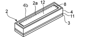
- FIG. 1 is a schematic perspective view showing a wavelength conversion member according to the first embodiment of the present invention.
- FIG. 2 is a schematic cross-sectional view taken along the line AA in FIG.
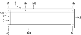
- FIG. 3 is a schematic plan view of the second main surface side of the side wall constituting the wavelength conversion member according to the first embodiment of the present invention.
- FIG. 4 is a schematic perspective view for explaining the method for manufacturing the wavelength conversion member according to the first embodiment of the present invention.
- FIG. 5 is a schematic perspective view for explaining the method for manufacturing the wavelength conversion member according to the first embodiment of the present invention.
- FIG. 6 is a schematic perspective view for explaining the method for manufacturing the wavelength conversion member according to the first embodiment of the present invention.
- FIG. 1 is a schematic perspective view showing a wavelength conversion member according to the first embodiment of the present invention.
- FIG. 2 is a schematic cross-sectional view taken along the line AA in FIG.
- FIG. 3 is a schematic plan view of the second main surface side of the side wall constituting the wavelength conversion
- FIG. 7 is a schematic perspective view for explaining the method for manufacturing the wavelength conversion member according to the first embodiment of the present invention.
- FIG. 8 is a schematic perspective view for explaining the method for manufacturing the wavelength conversion member according to the first embodiment of the present invention.
- FIG. 9 is a schematic plan view for explaining a laser irradiation method in the method of manufacturing a wavelength conversion member according to the first embodiment of the present invention.
- FIG. 10 is a schematic cross-sectional view showing a wavelength conversion member according to the second embodiment of the present invention.
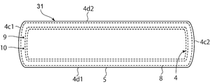
- FIG. 11 is a schematic plan view showing a wavelength conversion member according to the third embodiment of the present invention.
- FIG. 1 is a schematic perspective view showing a wavelength conversion member according to the first embodiment of the present invention.
- FIG. 2 is a schematic cross-sectional view taken along the line AA in FIG.
- the wavelength conversion member 1 includes a container 2, a resin 6, a phosphor 7, and a cover member 5.
- the resin 6 and the phosphor 7 constitute a resin layer 12.
- the resin layer 12 is filled in the recess 2 a of the container 2.
- the container 2 has a bottom plate 3 and a side wall 4.
- the planar shape of the bottom plate 3 is a rectangle.
- a frame-like side wall 4 is provided on the bottom plate 3.
- the side wall 4 has a first main surface 4a and a second main surface 4b facing each other.
- the first main surface 4a is disposed on the bottom plate 3 side.
- the second main surface 4 b is disposed on the side opposite to the bottom plate 3.
- Cover member 5 is arranged on second main surface 4b.
- the cover member 5 is provided so as to seal the container 2. More specifically, the cover member 5 is joined to the side wall 4 of the container 2 via the first glass frit 8.
- the first glass frit 8 is a glass frit that is melted by laser irradiation.
- FIG. 3 is a schematic plan view of the second main surface side of the side wall constituting the wavelength conversion member according to the first embodiment of the present invention.
- the side wall 4 has a pair of short sides 4c1, 4c2 facing each other and a pair of long sides 4d1, 4d2 facing each other.
- the short sides 4c1 and 4c2 and the long sides 4d1 and 4d2 are linear.
- the second main surface 4b is the main surface of the side wall 4 on the first glass frit 8 side.
- the laser scanning start point 9 and end point 10 are located on the second side 4c1 of the side wall 4 on the short side 4c1 side.
- the start point 9 and the end point 10 of the laser scanning may be provided on the short side 4 c 2 side on the second main surface 4 b of the side wall 4.
- the short side 4c1 side of the second main surface 4b includes corner portions 4f and 4g.
- the short side 4c2 side in the 2nd main surface 4b shall contain the corner
- the wavelength conversion member 1 converts the wavelength of the excitation light emitted from the light source. More specifically, excitation light enters from the bottom plate 3 in the wavelength conversion member 1. The incident excitation light passes through the bottom plate 3 and enters the resin layer 12. The phosphor 7 in the resin layer 12 is excited by the excitation light, and the fluorescence is emitted. The fluorescent light or the mixed light of the fluorescent light and the excitation light is emitted through the cover member 5.
- (Manufacturing method of wavelength conversion member) 4 to 8 are schematic perspective views for explaining the method for manufacturing the wavelength conversion member according to the first embodiment of the present invention.
- the container 2 is prepared as follows.
- a second glass frit 11 is printed on the bottom plate 3 and fired.
- the firing can be performed at a temperature of 300 ° C. to 550 ° C., for example.
- the side wall 4 is arranged on the bottom plate 3 so that the first main surface 4 a shown in FIG. 2 is placed on the portion where the second glass frit 11 is provided.
- the side wall 4 should just be provided so that at least one part may overlap with the part in which the 2nd glass frit 11 is provided in planar view. But it is preferable that the side wall 4 is provided so that it may overlap with the part in which the 2nd glass frit 11 is provided in planar view.
- the container 2 is obtained by baking with the side wall 4 disposed on the bottom plate 3 via the second glass frit 11.
- the firing can be performed, for example, in an electric furnace.
- the firing can be performed at a temperature of 590 ° C. to 650 ° C., for example.
- the container 2 may be one in which the bottom plate 3 and the side wall 4 are integrally formed.
- the first glass frit 8 is printed on the second main surface 4 b of the side wall 4 in the obtained container 2 and fired.
- the firing can be performed at a temperature of 300 ° C. to 550 ° C., for example.
- resin and phosphor are filled into the recess 2 a of the container 2 to form a resin layer 12.
- the resin layer 12 may be formed so as to completely fill the concave portion 2 a of the container 2, or may be formed so as to leave a part of the void in the concave portion 2 a of the container 2. Further, in the resin layer 12, it is desirable that the phosphor is dispersed in the resin.
- the cover member 5 is disposed on the second main surface 4 b of the side wall 4 in a portion where the first glass frit 8 is provided.
- the cover member 5 should just be provided so that at least one part may overlap with the part in which the 1st glass frit 8 is provided in planar view. But it is preferable that the cover member 5 is provided so that it may overlap with the part in which the 1st glass frit 8 is provided in planar view.
- the laser 14 is irradiated from the laser light source 13 to seal the recess 2 a of the container 2. Stop.
- the irradiation method of the laser 14 will be described in more detail with reference to FIG.
- FIG. 9 is a schematic plan view for explaining a laser irradiation method in the method of manufacturing a wavelength conversion member according to the first embodiment of the present invention.
- the starting point 9 is irradiated with laser.
- the laser is scanned along the direction of the arrow and circulated.
- the circulated laser is irradiated from the start point 9 to the end point 10.
- the recess of the container is sealed.
- the end point 10 of the laser scanning may be a position exceeding the starting point 9 after the laser is circulated, or may be the same position as the starting point 9. If the start point 9 and the end point 10 of the laser scanning are located on the short side 4c1 or the short side 4c2 side on the second main surface 4b of the side wall 4, there is no particular limitation.
- the start point 9 and the end point 10 of the laser scanning are located on the short side 4c1 or short side 4c2 side on the second main surface 4b of the side wall 4. Therefore, compared with the case where the start point 9 and the end point 10 of laser scanning are located on the long side 4d1 or the long side 4d2 side, cracks in the wavelength conversion member 1 are less likely to occur.
- the short sides 4c1 and 4c2 of the side wall 4 are short and thus are not easily deformed. That is, a large residual stress is applied to the side wall 4 on the short side 4c1 and 4c2 side. Does not occur.
- the long sides 4d1 and 4d2 of the side wall 4 are long, deformation is likely to occur, that is, a large residual stress is likely to be generated on the side wall 4 on the long side 4d1 and 4d2 side. Further, stress is also generated at the start point 9 and the end point 10 of the laser scanning.
- the residual stress is suppressed to an allowable range by positioning the laser scanning start point 9 and end point 10 on the short sides 4c1 and 4c2 side where only a small stress remains, rather than the long sides 4d1 and 4d2 side where a large stress remains. It is thought that it is possible.
- the length of the short sides 4c1 and 4c2 is preferably 4 mm or less, particularly preferably 3 mm or less.
- the length of the short sides 4c1 and 4c2 is preferably 0.2 mm or more, particularly 0.3 mm or more.
- the ratio of the lengths of the long sides 4d1 and 4d2 to the short sides 4c1 and 4c2 (long side / short side) is preferably 1.5 or more, more preferably 2.0 or more, and preferably 6.0 or less. Preferably it is 5.0 or less.
- the cover member 5 since the cover member 5 is not easily cracked particularly in the wavelength conversion member 1, the thickness of the cover member 5 can be reduced. Therefore, the wavelength conversion member 1 can be downsized.
- the thickness of the cover member 5 is preferably 0.2 mm or less, more preferably 0.1 mm or less.
- the container has a bottom plate and side walls.
- the side wall is provided on the bottom plate.
- the bottom plate can be made of a transparent material, for example.
- glass can be used as a material constituting the bottom plate.
- the glass include SiO 2 —B 2 O 3 —RO (R is Mg, Ca, Sr, or Ba) glass, SiO 2 —B 2 O 3 —R ′ 2 O (R ′ is Li, Na, or Ka).
- Series glass SiO 2 —B 2 O 3 —RO—R ′ 2 O (R is Mg, Ca, Sr or Ba, R ′ is Li, Na or Ka) series glass, SnO—P 2 O 5 series glass, TeO 2 -based glass or Bi 2 O 3 -based glass can be used.
- the side wall is preferably made of ceramics with high reflectivity. In this case, since excitation light and fluorescence can be reflected, the light utilization efficiency can be further enhanced.
- a ceramic with high reflectance for example, low temperature co-sintered ceramic (LTCC) can be mentioned.
- LTCC low temperature co-sintered ceramic
- alumina-glass ceramics can be used as the LTCC.
- the container may be formed by integrally molding the bottom plate and the side wall.
- the container in which the bottom plate and the side wall are integrally formed, it is possible to further suppress deformation of the container when the resin filled in the concave portion of the container is cured.
- the resin layer includes a resin and a phosphor.
- the phosphor is preferably dispersed in the resin.
- an ultraviolet curable resin or a thermosetting resin is used.
- an epoxy curable resin, an acrylic ultraviolet curable resin, a silicone curable resin, or the like can be used.
- quantum dots can be used.
- quantum dots include II-VI group compounds and III-V group compounds.
- the II-VI group compounds include CdS, CdSe, CdTe, ZnS, ZnSe, ZnTe and the like.
- the III-V group compound include InP, GaN, GaAs, GaP, AlN, AlP, AlSb, InN, InAs, and InSb. At least one selected from these compounds, or a composite of two or more of these can be used as quantum dots.
- the composite include those having a core-shell structure, such as those having a core-shell structure in which the surface of CdSe particles is coated with ZnS.
- the phosphor is not limited to quantum dots.
- oxide phosphor, nitride phosphor, oxynitride phosphor, chloride phosphor, acid chloride phosphor, sulfide phosphor, oxysulfide Inorganic phosphor particles such as a product phosphor, a halide phosphor, a chalcogenide phosphor, an aluminate phosphor, a halophosphate phosphor, or a garnet compound phosphor may be used.
- the first glass frit is a glass frit that is melted by laser irradiation.
- the first glass frit for example, a glass frit containing inorganic powder containing SnO-containing glass powder and a pigment can be used.
- the SnO-containing glass preferably contains SnO 35 to 70% and P 2 O 5 10 to 30% in terms of glass composition.
- SnO is a component that lowers the melting point of glass.
- P 2 O 5 is a component that enhances the thermal stability of the glass.
- SnO-containing glass ZnO, B 2 O 3, Al 2 O 3, SiO 2, In 2 O 3, Ta 2 O 5, La 2 O 3, MoO 3, WO 3, Li 2 O, Na 2 O , K 2 O, MgO, BaO or F 2 may be contained.
- the pigment is preferably an inorganic pigment, and more preferably contains at least one metal selected from Fe, Mn, Cu and the like or a compound containing the above metal in order to easily generate heat by absorbing laser light.
- a glass frit containing an inorganic powder containing a SnO-containing glass powder can be used as the second glass frit.
- the SnO-containing glass preferably contains SnO 35 to 70% and P 2 O 5 10 to 30% in terms of glass composition.
- SnO is a component that lowers the melting point of glass.
- P 2 O 5 is a component that enhances the thermal stability of the glass.
- SnO-containing glass ZnO, B 2 O 3, Al 2 O 3, SiO 2, In 2 O 3, Ta 2 O 5, La 2 O 3, MoO 3, WO 3, Li 2 O, Na 2 O , K 2 O, MgO, BaO or F 2 may be contained.
- the second glass frit preferably does not contain an inorganic pigment such as at least one metal selected from Fe, Mn and Cu or a compound containing the above metal. In that case, since the excitation light and fluorescence are not absorbed by the inorganic pigment, the light utilization efficiency can be further enhanced.
- an inorganic pigment such as at least one metal selected from Fe, Mn and Cu or a compound containing the above metal.
- the cover member can be made of a transparent material, for example.
- glass can be used as a material constituting the cover member.
- the glass include SiO 2 —B 2 O 3 —RO (R is Mg, Ca, Sr, or Ba) glass, SiO 2 —B 2 O 3 —R ′ 2 O (R ′ is Li, Na, or Ka).
- Series glass SiO 2 —B 2 O 3 —RO—R ′ 2 O (R is Mg, Ca, Sr or Ba, R ′ is Li, Na or Ka) series glass, SnO—P 2 O 5 series glass, TeO 2 -based glass or Bi 2 O 3 -based glass can be used.
- the bottom plate and the cover member are made of glass, the permeation of moisture and oxygen can be further suppressed. In this case, since the phosphor contained in the resin layer is less likely to deteriorate, a more reliable wavelength conversion member can be obtained.
- FIG. 10 is a schematic cross-sectional view of a wavelength conversion member according to the second embodiment of the present invention.
- a reflection member 22 is provided on the side surfaces of the container 2 and the cover member 5.
- a material which comprises the reflection member 22 For example, the ceramic and metal containing an alumina, a titania, etc. can be used. Other points are the same as in the first embodiment.
- the wavelength conversion member 21 since the start point and end point of laser scanning are located on the short side on the second main surface 4b of the side wall 4, the residual stress in the sealing portion by the laser is suppressed to an allowable range. be able to. Therefore, the wavelength conversion member 21 is hardly cracked. In particular, since the cover member 5 is not easily cracked in the wavelength conversion member 21, the thickness of the cover member 5 can be reduced, and the wavelength conversion member 21 can be downsized.
- the reflection member 22 is provided in the wavelength conversion member 21, excitation light and fluorescence can be reflected. Therefore, the light utilization efficiency can be further enhanced.
- the reflection member 22 is provided in the whole side surface of the container 2 and the cover member 5, the reflection member 22 may be provided only in the side surface of the side wall 4 in the container 2. As shown in FIG. Even in that case, excitation light and fluorescence can be reflected, and the utilization efficiency of light can be further enhanced.
- FIG. 11 is a schematic plan view of a wavelength conversion member according to the third embodiment of the present invention.
- the outer peripheral portions on the short side 4 c 1 side and the short side 4 c 2 side are each arcuate. Further, the short side 4c1 and the short side 4c2 of the side wall 4 are also arc-shaped. Other points are the same as in the first embodiment.
- the wavelength conversion member 31 since the laser scanning start point 9 and end point 10 are located on the short side 4c1 side on the second main surface of the side wall 4, the residual stress in the laser sealing portion is within an allowable range. Can be suppressed. Therefore, the wavelength conversion member 31 is not easily cracked. In particular, since the crack of the cover member 5 in the wavelength conversion member 31 is unlikely to occur, the thickness of the cover member 5 can be reduced, and the wavelength conversion member 31 can be downsized.
Landscapes
- Chemical & Material Sciences (AREA)
- Engineering & Computer Science (AREA)
- Geochemistry & Mineralogy (AREA)
- Life Sciences & Earth Sciences (AREA)
- Chemical Kinetics & Catalysis (AREA)
- General Chemical & Material Sciences (AREA)
- Materials Engineering (AREA)
- Organic Chemistry (AREA)
- Physics & Mathematics (AREA)
- Ceramic Engineering (AREA)
- General Physics & Mathematics (AREA)
- Optics & Photonics (AREA)
- Optical Filters (AREA)
Abstract
L'invention concerne un procédé de fabrication d'un élément de conversion de longueur d'onde dans lequel les craquelures provoquées par le scellage laser ne se produisent pas facilement. L'invention concerne un procédé de fabrication d'un élément de conversion de longueur d'onde (1) comprenant un récipient (2) ayant des parois latérales (4) sous la forme d'un cadre, de la résine et des phosphores qui remplissent l'intérieur du récipient (2) et un élément couvercle (5) disposé sur le dessus des parois latérales (4) du récipient (2) ; les parois latérales (4) comprenant une paire de côtés longs mutuellement opposés et une paire de côtés courts mutuellement opposés ; ledit procédé comprenant : une étape de préparation du récipient (2) ; une étape de remplissage de l'intérieur du récipient (2) avec la résine et les phosphores ; et une étape dans laquelle l'élément couvercle (5) est disposé sur les parois latérales (4) du récipient (2) avec une première fritte de verre (8) entre eux et la première fritte de verre est irradiée avec un laser et ainsi fondue, de manière à lier les parois latérales (4) du récipient (2) à l'élément couvercle (5) ; pendant l'irradiation laser, le laser est irradié et le récipient (2) est scellé, de sorte que le point de départ et le point de fin pour le balayage laser soient situés sur un côté court des parois latérales (4) du récipient (2).
Applications Claiming Priority (2)
| Application Number | Priority Date | Filing Date | Title |
|---|---|---|---|
| JP2016-048061 | 2016-03-11 | ||
| JP2016048061A JP2017161818A (ja) | 2016-03-11 | 2016-03-11 | 波長変換部材の製造方法及び波長変換部材 |
Publications (1)
| Publication Number | Publication Date |
|---|---|
| WO2017154355A1 true WO2017154355A1 (fr) | 2017-09-14 |
Family
ID=59790275
Family Applications (1)
| Application Number | Title | Priority Date | Filing Date |
|---|---|---|---|
| PCT/JP2017/001449 Ceased WO2017154355A1 (fr) | 2016-03-11 | 2017-01-18 | Procédé de fabrication d'élément de conversion de longueur d'onde, et élément de conversion de longueur d'onde |
Country Status (2)
| Country | Link |
|---|---|
| JP (1) | JP2017161818A (fr) |
| WO (1) | WO2017154355A1 (fr) |
Citations (11)
| Publication number | Priority date | Publication date | Assignee | Title |
|---|---|---|---|---|
| JP2010109128A (ja) * | 2008-10-30 | 2010-05-13 | Kyocera Corp | パッケージの製造方法 |
| WO2011065105A1 (fr) * | 2009-11-25 | 2011-06-03 | 浜松ホトニクス株式会社 | Procédé de soudage de verre et procédé de fixation de couche de verre |
| JP2011256092A (ja) * | 2010-06-11 | 2011-12-22 | Asahi Glass Co Ltd | 封着材料層付きガラス部材の製造方法及び製造装置、並びに電子デバイスの製造方法 |
| WO2012093698A1 (fr) * | 2011-01-06 | 2012-07-12 | 旭硝子株式会社 | Procédé et dispositif de fabrication d'éléments en verre comportant une couche de matériau d'étanchéité, et procédé de fabrication de dispositifs électroniques |
| WO2012098740A1 (fr) * | 2011-01-18 | 2012-07-26 | 日本電気硝子株式会社 | Dispositif électroluminescent, cellule pour dispositif électroluminescent, et procédé pour la fabrication de dispositif électroluminescent |
| WO2013150713A1 (fr) * | 2012-04-02 | 2013-10-10 | シャープ株式会社 | Dispositif d'affichage électroluminescent organique, et procédé de fabrication associé |
| JP2013239609A (ja) * | 2012-05-16 | 2013-11-28 | Asahi Glass Co Ltd | 気密部材とその製造方法 |
| JP2014015363A (ja) * | 2012-07-10 | 2014-01-30 | Hitachi Ltd | 焼成装置及びその制御方法 |
| WO2014092013A1 (fr) * | 2012-12-10 | 2014-06-19 | 旭硝子株式会社 | Matière de scellement, substrat comprenant une couche de matière de scellement, corps stratifié et dispositif électronique |
| JP2014225379A (ja) * | 2013-05-16 | 2014-12-04 | ソニー株式会社 | 発光装置、表示装置および照明装置 |
| US20150253482A1 (en) * | 2014-03-04 | 2015-09-10 | Samsung Display Co., Ltd. | Backlight assembly and display device having the same |
-
2016
- 2016-03-11 JP JP2016048061A patent/JP2017161818A/ja active Pending
-
2017
- 2017-01-18 WO PCT/JP2017/001449 patent/WO2017154355A1/fr not_active Ceased
Patent Citations (11)
| Publication number | Priority date | Publication date | Assignee | Title |
|---|---|---|---|---|
| JP2010109128A (ja) * | 2008-10-30 | 2010-05-13 | Kyocera Corp | パッケージの製造方法 |
| WO2011065105A1 (fr) * | 2009-11-25 | 2011-06-03 | 浜松ホトニクス株式会社 | Procédé de soudage de verre et procédé de fixation de couche de verre |
| JP2011256092A (ja) * | 2010-06-11 | 2011-12-22 | Asahi Glass Co Ltd | 封着材料層付きガラス部材の製造方法及び製造装置、並びに電子デバイスの製造方法 |
| WO2012093698A1 (fr) * | 2011-01-06 | 2012-07-12 | 旭硝子株式会社 | Procédé et dispositif de fabrication d'éléments en verre comportant une couche de matériau d'étanchéité, et procédé de fabrication de dispositifs électroniques |
| WO2012098740A1 (fr) * | 2011-01-18 | 2012-07-26 | 日本電気硝子株式会社 | Dispositif électroluminescent, cellule pour dispositif électroluminescent, et procédé pour la fabrication de dispositif électroluminescent |
| WO2013150713A1 (fr) * | 2012-04-02 | 2013-10-10 | シャープ株式会社 | Dispositif d'affichage électroluminescent organique, et procédé de fabrication associé |
| JP2013239609A (ja) * | 2012-05-16 | 2013-11-28 | Asahi Glass Co Ltd | 気密部材とその製造方法 |
| JP2014015363A (ja) * | 2012-07-10 | 2014-01-30 | Hitachi Ltd | 焼成装置及びその制御方法 |
| WO2014092013A1 (fr) * | 2012-12-10 | 2014-06-19 | 旭硝子株式会社 | Matière de scellement, substrat comprenant une couche de matière de scellement, corps stratifié et dispositif électronique |
| JP2014225379A (ja) * | 2013-05-16 | 2014-12-04 | ソニー株式会社 | 発光装置、表示装置および照明装置 |
| US20150253482A1 (en) * | 2014-03-04 | 2015-09-10 | Samsung Display Co., Ltd. | Backlight assembly and display device having the same |
Also Published As
| Publication number | Publication date |
|---|---|
| JP2017161818A (ja) | 2017-09-14 |
Similar Documents
| Publication | Publication Date | Title |
|---|---|---|
| JP5482378B2 (ja) | 発光装置 | |
| KR20170114919A (ko) | 발광 장치의 제조 방법 | |
| JP2010272847A5 (fr) | ||
| TWI746534B (zh) | 波長轉換構件及其製造方法、以及發光裝置 | |
| WO2018225424A1 (fr) | Convertisseur de longueur d'onde et son procédé de fabrication, et dispositif électroluminescent utilisant le convertisseur de longueur d'onde | |
| JP6874288B2 (ja) | 発光装置及びバックライト光源 | |
| US10644208B2 (en) | Method of manufacturing light emitting device | |
| JP4771800B2 (ja) | 半導体発光装置及びその製造方法 | |
| TW201810731A (zh) | 波長轉換構件及其製造方法、以及發光裝置 | |
| US20120140496A1 (en) | Wavelength conversion member, light emitting device, illuminating device, vehicle headlamp, and production method | |
| WO2023063103A1 (fr) | Dispositif fluorescent et dispositif électroluminescent | |
| WO2017154355A1 (fr) | Procédé de fabrication d'élément de conversion de longueur d'onde, et élément de conversion de longueur d'onde | |
| JP6658829B2 (ja) | 発光装置の製造方法 | |
| JP2018018871A (ja) | 波長変換部材及び発光デバイス | |
| JP2019045609A (ja) | 波長変換部材 | |
| JP2019091849A (ja) | パッケージ及び波長変換部材の製造方法 | |
| JP2018004975A (ja) | 波長変換部材及びその製造方法、並びに発光デバイス | |
| WO2018142910A1 (fr) | Procédé de fabrication d'un boîtier et d'un élément de conversion de longueur d'onde, boîtier, élément de conversion de longueur d'onde, dispositif électroluminescent, matériau de base de boîtier, et matériau de base de récipient | |
| JP7360054B2 (ja) | 発光装置の製造方法、接合方法、及び、発光装置 | |
| WO2018074170A1 (fr) | Dispositif électroluminescent | |
| JP6848582B2 (ja) | 波長変換部材及び発光デバイス | |
| WO2023058541A1 (fr) | Dispositif à luminophore et dispositif électroluminescent | |
| JP2024066549A (ja) | 蛍光体デバイス及び発光装置 | |
| JP2017151239A (ja) | 波長変換部材の製造方法 | |
| CN117438522A (zh) | 发光装置 |
Legal Events
| Date | Code | Title | Description |
|---|---|---|---|
| NENP | Non-entry into the national phase |
Ref country code: DE |
|
| 121 | Ep: the epo has been informed by wipo that ep was designated in this application |
Ref document number: 17762701 Country of ref document: EP Kind code of ref document: A1 |
|
| 122 | Ep: pct application non-entry in european phase |
Ref document number: 17762701 Country of ref document: EP Kind code of ref document: A1 |