WO2017154751A1 - Disque de réception d'échantillon et dispositif de détection de fluorescence l'utilisant - Google Patents
Disque de réception d'échantillon et dispositif de détection de fluorescence l'utilisant Download PDFInfo
- Publication number
- WO2017154751A1 WO2017154751A1 PCT/JP2017/008403 JP2017008403W WO2017154751A1 WO 2017154751 A1 WO2017154751 A1 WO 2017154751A1 JP 2017008403 W JP2017008403 W JP 2017008403W WO 2017154751 A1 WO2017154751 A1 WO 2017154751A1
- Authority
- WO
- WIPO (PCT)
- Prior art keywords
- signal
- sample storage
- track
- disk
- sample
- Prior art date
- Legal status (The legal status is an assumption and is not a legal conclusion. Google has not performed a legal analysis and makes no representation as to the accuracy of the status listed.)
- Ceased
Links
Images


Classifications
-
- G—PHYSICS
- G01—MEASURING; TESTING
- G01N—INVESTIGATING OR ANALYSING MATERIALS BY DETERMINING THEIR CHEMICAL OR PHYSICAL PROPERTIES
- G01N21/00—Investigating or analysing materials by the use of optical means, i.e. using sub-millimetre waves, infrared, visible or ultraviolet light
- G01N21/01—Arrangements or apparatus for facilitating the optical investigation
- G01N21/03—Cuvette constructions
-
- G—PHYSICS
- G01—MEASURING; TESTING
- G01N—INVESTIGATING OR ANALYSING MATERIALS BY DETERMINING THEIR CHEMICAL OR PHYSICAL PROPERTIES
- G01N21/00—Investigating or analysing materials by the use of optical means, i.e. using sub-millimetre waves, infrared, visible or ultraviolet light
- G01N21/62—Systems in which the material investigated is excited whereby it emits light or causes a change in wavelength of the incident light
- G01N21/63—Systems in which the material investigated is excited whereby it emits light or causes a change in wavelength of the incident light optically excited
- G01N21/64—Fluorescence; Phosphorescence
-
- G—PHYSICS
- G01—MEASURING; TESTING
- G01N—INVESTIGATING OR ANALYSING MATERIALS BY DETERMINING THEIR CHEMICAL OR PHYSICAL PROPERTIES
- G01N35/00—Automatic analysis not limited to methods or materials provided for in any single one of groups G01N1/00 - G01N33/00; Handling materials therefor
-
- G—PHYSICS
- G01—MEASURING; TESTING
- G01N—INVESTIGATING OR ANALYSING MATERIALS BY DETERMINING THEIR CHEMICAL OR PHYSICAL PROPERTIES
- G01N37/00—Details not covered by any other group of this subclass
Definitions
- the present invention relates to a sample storage disk for storing a sample prepared by fluorescently staining a subject such as a cell and a fluorescence detection apparatus using the same.
- Patent Document 1 discloses a technique for quickly and easily detecting such cells.
- a fluorescently labeled antigen to be detected is fixed to a track on a disc using the principle of a sandwich method using an antigen-antibody reaction. Thereafter, the track is scanned with laser light serving as excitation light to generate fluorescence from the antigen to be detected, and the antigen to be detected is detected and counted.
- address information in a radial direction and a track direction can be obtained from a disk by recording an address signal in advance in a track portion that is not connected to a flow path into which a sample flows. Describes that the position where the fluorescence is detected can be specified based on the address information.
- Detecting cells infected with pathogenic bacteria or cells having a predetermined form from a large number of cells is particularly important in the medical field such as clinical sites.
- an apparatus for performing such cell detection quickly and easily for example, an apparatus described in Patent Document 2 is known.
- a laser beam is irradiated to a sample containing target cells that are fluorescently labeled. Then, the fluorescence excited from the target cell by the laser light is detected by the photodetector. In this case, since the excited fluorescence is weak, the signal from the photodetector is easily affected by stray light.
- confocality is generated in the fluorescence, and stray light is removed by arranging a pinhole at the confocal position.
- the sample storage disk includes a substrate, a track formed on the upper surface of the substrate so as to turn around the center of the disk, and a sample storage unit disposed on the upper side of the track to store the sample.
- the track is configured to be scanned in the scanning direction. Address signals indicating the positions of the track portions are respectively recorded on the upstream side and the downstream side of the sample storage portion in the scanning direction of the track portion straddling the sample storage portion of the track.
- This sample storage disk can acquire a fluorescent image smoothly.
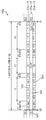
- FIG. 1A is a plan view schematically showing a configuration of a sample storage disk according to the first embodiment.
- FIG. 1B is a view of the sample storage disk shown in FIG. 1A along line 1B-1B.
- FIG. 2 is a diagram schematically showing the structure of grooves, lands, and pits of the sample storage disk according to the first embodiment.
- FIG. 3A is a plan view schematically showing area division in the circumferential direction of the sample storage disk according to the first embodiment.
- FIG. 3B is a plan view schematically showing the zoning in the radial direction of the sample storage disk according to the first embodiment.
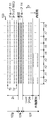
- FIG. 4 is a diagram in which the grooves and lands of each zone of the sample storage disk according to the first embodiment are linearly developed.
- FIG. 5A is a diagram illustrating a format of each field set in a track portion (groove) of one area of the sample storage disk according to the first embodiment.
- FIG. 5B is a diagram schematically illustrating an angle range of each field of the sample storage disk according to the first embodiment.
- FIG. 6A is a diagram illustrating a signal format of each field of the sample storage disk according to the first embodiment.
- FIG. 6B is a schematic enlarged view of the sample storage disk according to the first embodiment.
- FIG. 7 is a configuration diagram of a fluorescence detection pickup for reading fluorescence from the sample storage disk according to the first embodiment.
- FIG. 8 is a diagram illustrating a configuration of a signal calculation circuit of the fluorescence detection pickup according to the first embodiment.
- FIG. 9 is a configuration diagram of the fluorescence detection apparatus according to the first embodiment.
- FIG. 10A is a flowchart illustrating an address signal acquisition process of the fluorescence detection device according to the first embodiment.
- FIG. 10B is a flowchart illustrating the fluorescence signal extraction processing of the fluorescence detection apparatus according to the first embodiment.
- FIG. 11A is a flowchart illustrating a fluorescence signal cut-out process of the fluorescence detection device according to the first embodiment.
- FIG. 11B is a flowchart illustrating a cut-out signal invalidation process of the fluorescence detection device according to the first embodiment.
- FIG. 12 is a diagram for explaining a fluorescence signal cut-out process of the fluorescence detection device according to the first embodiment.
- FIG. 13 is a diagram in which grooves and lands in each zone of the sample storage disk according to the second embodiment are linearly developed.
- FIG. 14A is a diagram illustrating a format of each field set in a track portion of one area of the sample storage disk according to the second embodiment.
- FIG. 14B is a diagram illustrating a configuration for inverting the polarity of the tracking error signal of the fluorescence detection device according to the second embodiment.
- FIG. 14C is a diagram schematically illustrating beam scanning and polarity inversion timing of the tracking error signal in the fluorescence detection device according to the second exemplary embodiment.
- FIG. 14D is a diagram schematically illustrating the structure of grooves, lands, and pits of another sample storage disk according to the second embodiment.
- FIG. 15A is a diagram illustrating a part of the signal format of the sample storage disk according to the third embodiment.
- FIG. 15B is a diagram illustrating a part of the signal format of the sample storage disk according to the third embodiment.
- FIG. 15C is a diagram schematically illustrating the configuration of the synchronization adjustment pit SB1 of the sample storage disk according to the third embodiment.
- FIG. 16 is a diagram illustrating a configuration of the fluorescence detection apparatus according to the third embodiment.
- FIG. 17A is a diagram schematically illustrating the detection position of the synchronization adjustment pit on the signal light image of the fluorescence detection device according to the third exemplary embodiment.
- FIG. 17B is a diagram schematically illustrating a fluorescence image correction process of the fluorescence detection device according to the third embodiment.
- FIG. 17C is a diagram schematically illustrating a fluorescence image correction process of the fluorescence detection device according to the third embodiment.
- FIG. 18 is a diagram illustrating a part of a signal format of another sample storage disk according to the third embodiment.
- FIG. 19 is a diagram illustrating a format of each field set in a track portion (groove) of one area according to the fourth embodiment.
- FIG. 20 is a diagram illustrating a signal format of each field according to the fourth embodiment.
- FIG. 21 is a configuration diagram of a signal calculation circuit and an output processing circuit of the fluorescence detection apparatus according to the fourth embodiment.
- FIG. 22 is a configuration diagram of the fluorescence detection apparatus according to the fourth embodiment.
- FIG. 23A is a configuration diagram of an output processing circuit of a fluorescence detection device of a comparative example.
- FIG. 23B is a diagram schematically illustrating a reproduction RF signal input to the AD conversion circuit of the output processing circuit of the comparative example.
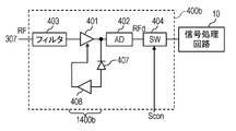
- FIG. 24A is a configuration diagram of an output processing circuit of the fluorescence detection apparatus according to the fourth embodiment.
- FIG. 24B is a diagram schematically illustrating a reproduction RF signal input to the AD conversion circuit of the output processing circuit when the modulation structure is not formed in the groove of the fluorescence detection device according to the fourth exemplary embodiment.
- FIG. 24C is a diagram schematically illustrating a reproduction RF signal input to the AD conversion circuit of the output processing circuit when the modulation structure is formed in the groove of the fluorescence detection device according to the fourth exemplary embodiment.
- FIG. 25A is a configuration diagram of another output processing circuit according to the fourth embodiment.
- FIG. 25B is a configuration diagram of still another output processing circuit according to the fourth embodiment.
- FIG. 25C is a diagram showing a format of a track area of another sample storage disk according to the fourth embodiment.
- FIG. 26A is a flowchart illustrating a process of stopping the output of various signals from the output processing circuit of the fluorescent device according to the fourth embodiment.
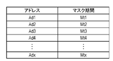
- FIG. 26B is a diagram illustrating a configuration of a table referred to in setting a mask period of the fluorescence detection apparatus according to the fourth embodiment.
- FIG. 27 is a diagram showing the format of each field set in the track portion of one area of the sample storage disk according to the fifth embodiment.
- FIG. 28A is a diagram in which grooves and lands of other sample storage disks according to Embodiments 4 and 5 are linearly developed.
- FIG. 28B is a diagram in which grooves and lands of still another sample storage disk according to Embodiments 4 and 5 are linearly developed.
- FIG. 29 is a configuration diagram of the fluorescence detection pickup according to the sixth embodiment.
- FIG. 30A is a configuration diagram of a light shielding body of the fluorescence detection pickup according to the sixth embodiment.
- FIG. 30B is a configuration diagram of another light shielding body of the fluorescence detection pickup according to the sixth embodiment.
- FIG. 30C is a cross-sectional view of the light-shielding unit of the fluorescence detection pickup according to the sixth embodiment.
- FIG. 31 is a cross-sectional view of the light shielding unit according to the sixth embodiment.
- FIG. 32A is a cross-sectional view of the light shielding unit according to Embodiment 6.
- FIG. 32B is a cross-sectional view of another light shielding unit according to Embodiment 6.
- FIG. 33A is a cross-sectional view of still another light shielding unit according to Embodiment 6.
- FIG. 33B is a cross-sectional view of still another light shielding unit according to Embodiment 6.
- FIG. 33A is a cross-sectional view of still another light shielding unit according to Embodiment 6.
- FIG. 33C is a cross-sectional view of still another light shielding unit according to Embodiment 6.
- FIG. 34A is a cross-sectional view of still another light shielding unit according to Embodiment 6.
- FIG. 34B is a cross-sectional view of still another light shielding unit according to Embodiment 6.
- FIG. 35 is a configuration diagram of still another fluorescence detection pickup according to the sixth embodiment.
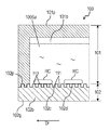
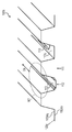
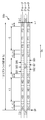
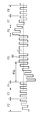
- FIG. 1A is a plan view schematically showing an external configuration of a sample storage disk 100 in the first embodiment.
- FIG. 1B is a cross-sectional view of the sample storage disk shown in FIG. 1A taken along line 1B-1B.
- FIG. 1B is a partially enlarged view of the sample storage disk 100 cut along a plane perpendicular to the disk surface and passing through the disk center Pc. Show.
- the sample storage disk 100 is used, for example, to detect red blood cells infected with malaria parasites.
- the sample storage disk 100 has a disk shape like an optical disk (CD, DVD, etc.), and a circular opening 101a is formed at the disk center Pc.
- the sample storage disk 100 includes a substrate 102 and a substrate 101 bonded to the upper surface 102p of the substrate 102.
- the substrate 101 constitutes a sample storage unit 101b. Both the substrate 101 and the substrate 102 are made of a resin material.
- the substrate 102 is made of a material that can transmit light.
- FIG. 1A By bonding the substrate 101 to the upper surface 102p of the substrate 102, nine sample accommodating portions 101b are formed as shown in FIG. 1A. These sample storage portions 101b are arranged at regular intervals in the disk circumferential direction Dc. Further, two boundaries (ends) of the sample storage unit 101b arranged in the disk circumferential direction Dc extend radially from the disk center Pc so as to be away from the disk center Pc. The nine sample storage portions 101b extend over an angular range Wa centered on the disc center Pc. As shown in FIG. 1B, the sample container 101b is a space having a predetermined height. When viewed from above, the sample storage unit 101b has a trapezoidal shape with rounded corners. The nine sample storage portions 101b have the same shape and are arranged at the same position in the disk radial direction Dr perpendicular to the disk circumferential direction Dc from the disk center Pc.
- Two holes 101c that continue to the upper surface 101p of the sample container 101b are formed on the inner peripheral side of the sample container 101b that faces the disk center Pc.
- the sample storage portion 101b is filled with the sample 100Sa from the one hole 101c.
- Sample 100Sa is prepared such that the malaria parasite in red blood cells RC is labeled with a fluorescent dye.
- the two holes 101c are closed with a lid.
- the sample 100Sa prepared from nine types of specimens is filled in the sample storage unit 101b.
- FIG. 1B schematically shows the red blood cells RC stored in the sample storage unit 101b.
- the track 102c is composed of a series of grooves 111 that spirally turn around the disk center Pc. Groove 111 is formed in the track area 102a indicated by hatching in FIG. 1A from the outermost circumference that is the outermost edge farthest from the disk center Pc of the track area 102a to the innermost circumference that is the outermost edge closest to the disk center Pc.
- the substrate 102 is formed by injection molding by the same process as that for CD and DVD.
- the semi-transmissive film 102d is formed by a sputtering process.
- the semi-transmissive film 102d reflects a part of the laser beam incident from the lower surface 102q of the substrate 102 from the lower surface 102dq of the semi-transmissive film 102d, and transmits the rest of the laser light to the semi-transmissive film 102d, thereby forming the semi-transmissive film 102d.
- the sample is guided to the sample container 101b through the upper surface 102dp.
- the semi-transmissive film 102d transmits the fluorescence generated in the sample storage portion 101b to the substrate 102 through the lower surface 102q.
- the reflectivity of the semi-transmissive film 102d is set to about 5% to 20% so that more laser light can be guided to the sample container 101b and more fluorescence can be transmitted to the substrate 102. .
- the sample storage disk 100 is divided into nine areas A0 to A8 in the disk circumferential direction Dc. Each area includes one sample container 101b. As will be described later, one track portion Ta in each area of the track 102c constitutes one unit of information recording area. Various signals are recorded in portions of the track portion Ta that do not overlap the sample storage portion 101b when viewed from above. In the present embodiment, these signals are recorded by a pit string composed of one or more pits.
- FIG. 2 is an enlarged view of the semi-transmissive film 102d located on the upper surface 102p of the substrate 102, and schematically shows the structure of the groove 111, the land 112, and the pit 113.
- FIG. 2 shows only the semipermeable membrane 102d. 2 is the substrate 102 side. That is, in FIG. 2, the upper surface 102dp of the semi-permeable membrane 102d faces downward and the lower surface 102dq faces upward.
- a groove 111 is formed on the substrate 102 (semi-transmissive film 102d).
- the lands 112 connected to the grooves 111 and between the grooves 111 constitute an upper surface 102 p of the substrate 102.
- a pit 113 is formed in a groove 111 corresponding to a portion of the track portion Ta that does not overlap the sample accommodating portion 101b, and a predetermined signal is recorded.
- the groove 111 includes pits 113 and spaces 113s. In the space 113s, the pit 113 is not formed, and the groove 111 extends monotonously. The format of the signal to be recorded will be described later. No signal is recorded on the land 112 between adjacent grooves 111. Further, the groove 111 and the land 112 extend spirally around the disc center Pc without meandering.
- the beam spot B1 of the laser beam applied to the lower surface 102q of the substrate 102 moves relatively along the groove 111 and scans the track 102c in the scanning direction Ds.
- the beam spot B1 scans the groove 111 (track 102c) from the outermost peripheral part farthest from the disk center Pc of the groove 111 toward the innermost peripheral part closest to the disk center Pc.
- the laser beam forming the beam spot B1 hits the lower surface 102dq of the semi-transmissive film 102d, a part of the laser beam is reflected by the lower surface 102q as described above and becomes reflected light.
- the intensity of the reflected light from the groove 111 decreases.
- the reflected light is modulated by the pits 113 and the intensity of the reflected light changes.
- the photodetector receives the modulated reflected light and outputs a detection signal that changes according to the intensity of the reflected light. By demodulating the detection signal, various information recorded in the pit 113 is reproduced.
- the diameter of the beam spot B1 is substantially the same as the pitch of the tracks 102c (grooves 111) extending spirally in the disc radial direction Dr, that is, the track pitch that is the interval between the track portions Ta adjacent to each other in the disc radial direction Dr. In the first embodiment, the track pitch is about 0.3 ⁇ m to 2.0 ⁇ m.
- FIG. 3A is a plan view of the sample storage disk 100, schematically showing areas A0 to A8 arranged in the disk circumferential direction Dc.
- FIG. 3B is a plan view of the sample storage disk 100.
- the track region 102a of the sample storage disk 100 is divided into a plurality of zones Z0 to Zn arranged in the disk radial direction Dr.
- FIG. 3B schematically shows a plurality of zones Z0 to Zn.
- Areas A0 to A8 shown in FIG. 3A and zones Z0 to Zn shown in FIG. 3B are logically assigned to the sample storage disk 100 in order to set a signal format to be described later on the track 102c in relation to the sample storage unit 101b. It is a thing and is not divided by physical structures, such as a barrier and a groove
- the sample storage disk 100 is divided into a plurality of areas at a predetermined constant angular interval with respect to the disc center Pc.
- nine areas are provided at an angular interval of 40 degrees with respect to the disc center Pc. It is divided into A0 to A8.
- the track portion included in each area is the track portion Ta in FIG. 1A.
- the track area 102a shown in FIG. 1A is detected between the outer area 102e farthest from the disk center Pc, the inner area 102f closest to the disk center Pc, and the outer area 102e and the inner area 102f in the disk radial direction Dr. It is divided into an area 102g.
- the outer area 102e is a lead-in area
- the inner area 102f is a lead-out area and an appearance identification area.
- the groove 111 of the lead-in area (outer area 102e), various information necessary for scanning the sample storage disk 100 is recorded in pit rows.
- a signal indicating the lead-out area is recorded as a pit string.
- the appearance identification area (inner area 102f) is provided with a structure for visually displaying the type and the like of the sample storage disk 100 by making the groove 111 discontinuous. The appearance identification area is set on the inner circumference side closer to the disk center Pc of the lead-out area.
- the detection region 102g of the sample storage disk 100 is divided into a plurality of zones Z0 to Zn in the disk radial direction Dr.
- the sample storage disk 100 is divided into, for example, 75 zones.
- the number of track portions arranged in the disk radial direction Dr included in each zone in the track 102c is the same.
- the track 102c (groove 111) of one zone is scanned by the beam spot B1 at the same angular velocity with respect to the disc center Pc.
- the angular velocity of each zone is set so that the track portion Ta of the track 102c (groove 111) at the center position of the zone in the disc radial direction Dr is scanned by the beam spot B1 at the same linear velocity.
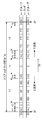
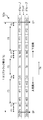
- FIG. 4 shows the groove 111 and the land 112 of each zone developed in a straight line.
- the groove 111 and the land 112 for one round are shown by one straight line.
- the lengths of the grooves 111 and lands 112 shown in FIG. 4 are not physical lengths, but are standardized so that the length of one round is the same in all the grooves 111 and lands 112 for convenience. Has been.
- the detection area 102g is divided into a plurality of zones Z0 to Zn in the disk radial direction Dr.
- Each zone includes a plurality of tracks 102c (grooves 111) arranged in the disk radial direction Dr.
- track numbers T0 to Tm from the outer peripheral side are given to the track portion Ta of the track 102c in one zone.
- the number of track portions Ta of the track 102c included in one zone is, for example, 800.
- FIG. 5A shows a format of fields F1 to F9 set in each of a plurality of track portions Ta (groove 111) in each area Ax of areas A0 to A8.
- FIG. 5B schematically shows the angle range of the fields F1 to F9.
- fields F1 to F9 are set in each of a plurality of track portions Ta (groove 111) in one area Ax.
- the fields F2, F5, and F7 no signal is recorded in the pit 113 (see FIG. 2), and only the groove 111 (G) including only the monotonically extending space 113s (see FIG. 2) is formed.
- the field F5 overlaps the sample storage portion 101b in the entire length. That is, both ends of the field F5 coincide with two boundaries (ends) arranged in the disk circumferential direction Dc of the sample storage unit 101b. Therefore, no signal is recorded on the track portion that overlaps the sample storage portion 101b when viewed from above, and only the groove 111 that extends monotonously and flat is formed.
- the track portion Ta starts at the start end SP and ends at the end EP along the scanning direction Ds.
- the start ends SP of all track portions Ta within the same area are aligned in one disk radial direction Dr1, that is, located on a straight line Lr1 extending from the disk center Pc in the disk radial direction Dr1.
- the end points EP of all track portions Ta in the same area are aligned in one disc radial direction Dr, that is, located on a straight line Lr2 extending from the disc center Pc in the disc radial direction Dr2.
- the start ends of the fields F5 in all the track portions Ta in the same area are aligned in the disc radial direction Dr, and the end ends of the field F5 are aligned in another disc radial direction Dr.
- the start ends of the field F1 in all the track portions Ta in the same area are aligned in another disk radial direction Dr, and the ends of the field F1 are aligned in another disk radial direction Dr.
- the start ends of the field F3 in all the track portions Ta in the same area are aligned in another disk radial direction Dr, and the ends of the field F3 are aligned in another disk radial direction Dr.
- the start ends of the fields F4 in all track portions Ta in the same area are aligned in another disk radial direction Dr, and the ends of the field F4 are aligned in another disk radial direction Dr.
- the start ends of the fields F6 in all the track portions Ta in the same area are aligned in another disk radial direction Dr, and the ends of the field F6 are aligned in another disk radial direction Dr.
- the start ends of the field F8 in all the track portions Ta in the same area are aligned in another disk radial direction Dr, and the ends of the field F8 are aligned in another disk radial direction Dr.
- the start ends of the fields F9 in all the track portions Ta in the same area are aligned in another disk radial direction Dr, and the ends of the field F9 are aligned in another disk radial direction Dr.
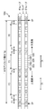
- FIG. 6A shows a signal format of the fields F1 to F9 of a certain track portion Ta1 among the plurality of track portions Ta.
- Each of the plurality of track portions Ta has the same configuration as the track portion Ta1.
- a hatched portion indicates a region where the pit 113 is formed in the groove 111, and a white portion where the hatched hatch is not illustrated indicates a region of only the groove 111 where the pit 113 is not formed.
- the time length 1T indicates the time length of the minimum pit when the groove 111 is scanned at a constant angular velocity as described above.
- a signal En composed of pits and spaces that are alternately repeated 10 times is recorded. Both the pit and the space of the signal En have a time length 2T that is twice the time length 1T.
- the signal En recorded in the field F1 indicates the start point SP (see FIG. 5A) of the track portion Ta1 of one area, and the signal En recorded in the field F9 is the end point EP of the track portion Ta1 of one area (see FIG. 5A). ).
- the pits 113 are not formed in the fields F2, F5, and F7, and the fields F2, F5, and F7 are composed of only the space 113s.
- Field F4 starts with a space having a time length 8T which is eight times the time length 1T, a pit having a time length 1T and a space having a time length 1T which are alternately repeated four times after the space.
- a signal V3 is recorded.
- the start signal V3 indicates a position where the sample storage unit 101b starts in the scanning direction Ds.
- an end signal Vs composed of repeated pits and spaces alternately 5 times is recorded. Both the pit and space of the end signal Vs have a time length 4T that is four times the time length 1T.
- the end signal Vs indicates a position where the sample storage unit 101b ends along the scanning direction Ds.
- the field F3 is composed of three header areas HE0 to HE2.
- the header area HE0 is a reserved area in which an arbitrary signal not defined by the format can be recorded.
- an identification signal for identifying the header area HE1 an address signal indicating the position of the track portion Ta1, and an error correction signal for performing error detection or error correction on the address signal are recorded. These signals have a fixed bit length.
- the address signal includes the track number of the track portion Ta1 of the track numbers T0 to Tm shown in FIG. 4, the zone number indicating the zone including the track portion Ta1 of the zones Z0 to Zn, and the areas A0 to A9. And an area number indicating an area including the track portion Ta1.
- signals similar to those in the header area HE1 are recorded.
- the field F8 includes three footer areas FT0 to FT2.
- the footer area FT0 is a reserved area like the header area HE0.
- an identification signal, an address signal, and an error correction signal are recorded. These signals have a fixed bit length.
- the address signal includes the track number of the track portion Ta1 of the track numbers T0 to Tm, the zone number indicating the zone including the track portion Ta1 of the zones Z0 to Zn, and the track portion Ta1 of the areas A0 to A9.
- the area number indicating the area to be included is included.
- a signal similar to that in the footer area FT1 is recorded.
- the identification signals in the footer areas FT1 and FT2 are different from the identification signals in the header areas HE1 and HE2.
- the address signals in the footer areas FT1 and FT2 are the same as the address signals in the header areas HE1 and HE2.
- digital signals (bit signals) having values of 1 and 0 are recorded depending on pits and spaces.
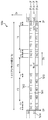
- FIG. 6B is a schematic enlarged view of the sample storage disk 100, and shows a field F4 in a track portion Ta of track numbers T11 to T15. As shown in FIG.
- a space Sc1 having a time length 8T, a pit Pt1 having a time length 1T, and a space Sc2 having a time length 1T along the scanning direction Ds A pit Pt2 having a time length 1T, a space Sc3 having a time length 1T, a pit Pt3 having a time length 1T, a space Sc4 having a time length 1T, a pit Pt4 having a time length 1T, and a time length 1T Space Sc5 is arranged in this order. As shown in FIG.
- both ends of the space Sc1 of the field F4 in all the track portions Ta of each zone including the track numbers T11 to T15 are aligned in the disk radial directions Dr11 and Dr12 that are separated from the disk center Pc. And located on straight lines Lr11 and Lr12 extending in the disk radial direction Dr11 and Dr12 from the disk center Pc, respectively.
- Both ends of the pit Pt1 of the field F4 of all the track portions Ta of each zone of each area including the track numbers T11 to T15 are aligned in the disk radial directions Dr12 and Dr13 away from the disk center Pc, and the disk diameter from the disk center Pc. They are located on straight lines Lr12 and Lr13 extending in directions Dr12 and Dr13, respectively.
- Both ends of the space Sc2 of the field F4 of all track portions Ta of each zone of each area including the track numbers T11 to T15 are aligned in the disk radial directions Dr13 and Dr14 away from the disk center Pc, and the disk diameter from the disk center Pc. They are located on straight lines Lr13 and Lr14 extending in directions Dr13 and Dr14, respectively. Both ends of the pit Pt2 of the field F4 of all track portions Ta of each zone of each area including the track numbers T11 to T15 are aligned in the disk radial directions Dr14 and Dr15 away from the disk center Pc, respectively. They are located on straight lines Lr14 and Lr15 extending in directions Dr14 and Dr15, respectively.
- Both ends of the space Sc3 of the field F4 of all track portions Ta of each zone of each area including the track numbers T11 to T15 are aligned in the disk radial directions Dr15 and Dr16 away from the disk center Pc, and the disk diameter from the disk center Pc. They are located on straight lines Lr15 and Lr16 extending in the directions Dr15 and Dr16, respectively.
- Both ends of the pit Pt3 of the field F4 of all track portions Ta of each zone of each area including the track numbers T11 to T15 are aligned in the disc radial directions Dr16 and Dr17, respectively, away from the disc center Pc. They are located on straight lines Lr16 and Lr17 extending in directions Dr16 and Dr17, respectively.
- Both ends of the space Sc4 of the field F4 of all the track portions Ta of each zone of each area including the track numbers T11 to T15 are aligned in the disk radial directions Dr17 and Dr18 away from the disk center Pc. They are located on straight lines Lr17 and Lr18 extending in the directions Dr17 and Dr18, respectively. Both ends of the pit Pt4 of the field F4 of all track portions Ta of each zone of each area including the track numbers T11 to T15 are aligned in the disc radial directions Dr18 and Dr19, respectively, away from the disc center Pc. They are located on straight lines Lr18 and Lr19 extending in directions Dr18 and Dr19, respectively.
- Both ends of the space Sc5 of the field F4 of all the track portions Ta of each zone of each area including the track numbers T11 to T15 are aligned in the disk radial directions Dr19 and Dr110 that are separated from the disk center Pc, and the disk diameter from the disk center Pc. They are located on straight lines Lr19 and Lr110 extending in directions Dr19 and Dr110, respectively.
- the pits and spaces formed in the fields F1 and F9 are aligned in the disc radial direction Dr in the track portion Ta included in all the zones of the same area. Since the pits and spaces formed in the fields F3 and F8 have different time lengths depending on the contents of the address signal, the positions of the pits and spaces in the plurality of track portions Ta are shifted in the disk circumferential direction Dc.
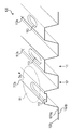
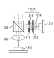
- FIG. 7 is a configuration diagram of a fluorescence detection pickup 200 for reading fluorescence from the sample storage disk 100.
- fluorescence is detected from the sample storage portion 101 b of the sample storage disk 100 using the fluorescence detection pickup 200.
- fluorescence is detected from the sample storage disk 100 to determine whether the red blood cells RC are infected with malaria parasites.
- the sample 100Sa is prepared so that the malaria parasite in the red blood cells RC is labeled with a fluorescent dye.
- the fluorescent dye when the fluorescent dye is irradiated with light having a wavelength of 405 nm, the fluorescent dye generates fluorescence having a wavelength of about 450 to 540 nm.
- the sample 100Sa thus prepared is filled into the nine sample storage portions 101b of the sample storage disk 100 for each specimen. Thereafter, the opening 101a (see FIG. 1A) of the sample storage disk 100 is fixed to the turntable 230 supported by the spindle motor 220.
- the fluorescence detection pickup 200 includes a semiconductor laser 201, a half-wave plate 202, a polarizing beam splitter (PBS) 203, a collimator lens 204, a quarter-wave plate 205, an objective lens 206, and an objective lens actuator. 207, a dichroic prism 208, an anamorphic lens 209, a photodetector 210, and a fluorescence detector 211.
- PBS polarizing beam splitter
- the semiconductor laser 201 emits a laser beam having a wavelength of about 405 nm.
- the polarization direction of the laser light emitted from the semiconductor laser 201 is adjusted by the half-wave plate 202 so as to be S-polarized with respect to the PBS 203.
- the laser beam is reflected by the PBS 203 and enters the collimator lens 204.
- the PBS 203 has polarization dependency of characteristics such as reflection and transmission only for light near the wavelength of the laser light emitted from the semiconductor laser 201, and has a wavelength other than the wavelength of the laser light, for example, a wavelength of about 450 to 540 nm. Light does not have polarization dependency of the above characteristics.
- the collimator lens 204 converts laser light incident from the PBS 203 side into parallel light.
- the quarter-wave plate 205 converts the laser light incident from the collimator lens 204 side into circularly polarized light, and the polarization direction when the laser light incident from the objective lens 206 side is incident from the collimator lens 204 side.
- the laser light reflected by the semi-transmissive film 102d of the sample storage disk 100 passes through the PBS 203 as it is and is not reflected toward the fluorescence detector 211.
- the objective lens 206 converges the laser light incident from the 1 ⁇ 4 wavelength plate 205 side on the semi-transmissive film 102d of the sample storage disk 100.
- the objective lens actuator 207 is displaced by driving the objective lens 206 in the focus direction and the tracking direction so that the laser beam converges on the groove 111 of the sample storage disk 100 by a servo circuit 50 (see FIG. 9) described later.
- the dichroic prism 208 transmits light having a wavelength of about 405 nm of the laser light emitted from the semiconductor laser 201 and reflects light having a fluorescence wavelength other than the wavelength of the laser light emitted from the semiconductor laser 201, for example, about 450 to 540 nm. It is configured as follows. As a result, the fluorescence incident from the PBS 203 side is reflected by the dichroic prism 208, and the laser light incident from the PBS 203 side passes through the dichroic prism 208.
- the anamorphic lens 209 introduces astigmatism into the laser light transmitted through the dichroic prism 208.
- the laser light that has passed through the anamorphic lens 209 enters the photodetector 210.
- the photodetector 210 has a four-divided sensor for receiving laser light on the light receiving surface.
- the detection signal output from the photodetector 210 is processed by a signal arithmetic circuit 300 (see FIG. 8) described later.
- the fluorescence reflected by the dichroic prism 208 is guided to the light receiving surface of the fluorescence detector 211 while being converged by the collimator lens 204.
- the fluorescence detector 211 has a sensor for receiving fluorescence by being provided on the light receiving surface.
- the detection signal of the fluorescence detector 211 is amplified by a signal amplification circuit.
- a barrier for preventing the laser light emitted from the semiconductor laser 201 from entering the fluorescence detector 211 is optically appropriately used. It is preferable to arrange in the system.
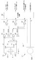
- FIG. 8 is a configuration diagram of the signal arithmetic circuit 300 according to the first embodiment.
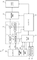
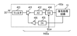
- FIG. 9 is a configuration diagram of the fluorescence detection apparatus 1 according to the first embodiment.
- the light detector 210 has a quadrant sensor for receiving laser light as described above.
- the upper left sensor 2101, the upper right sensor 2102, the lower right sensor 2103, and the lower left sensor 2104 of the quadrant sensor output detection signals S1, S2, S3, and S4 based on the beam spot of the received laser beam, respectively.
- the signal arithmetic circuit 300 processes the detection signals S1 to S4 to generate a focus error signal FE, a tracking error signal TE, and a reproduction RF signal RF.
- the focus error signal FE and the tracking error signal TE are generated according to the astigmatism method and the one-beam push-pull method used in existing optical disc apparatuses.
- the signal operation circuit 300 includes adders 301 to 304 and 307 and subtractors 305 and 306.
- the adder 301 outputs a signal (S1 + S3) obtained by adding the detection signals S1 and S3 to the subtractor 305
- the adder 302 outputs a signal (S2 + S4) obtained by adding the detection signals S2 and S4 to the subtractor 305.
- the adder 303 outputs a signal (S1 + S4) obtained by adding the detection signals S1 and S4 to the subtractor 306 and the adder 307
- the adder 304 adds the signal (S2 + S3) obtained by adding the detection signals S2 and S3 to the subtractor 306. And output to the adder 307.
- the subtracter 305 subtracts the output signal of the adder 302 from the output signal of the adder 301 and outputs a focus error signal FE.
- the subtracter 306 subtracts the output signal of the adder 304 from the output signal of the adder 303 and outputs a tracking error signal TE.
- the adder 307 adds the output signals of the adders 303 and 304 and outputs a reproduction RF signal RF (SUM signal).
- the focal position of the objective lens 206 when the focal position of the objective lens 206 is positioned on the semi-transmissive film 102d of the sample storage disk 100, the beam spot on the four-divided sensors 2101 to 2104 of the photodetector 210 becomes a minimum circle of confusion, and a focus error signal.
- the value of FE becomes 0.
- the focal position of the objective lens 206 is positioned at the center position in the disk radial direction Dr of the track 102c (groove 111) of the sample storage disk 100, the beam spots on the quadrant sensors 2101 to 2104 of the photodetector 210.
- the size of the portion applied to the left two sensors 2101 and 2104 is equal to the size of the portion applied to the two right sensors 2102 and 2103, and the value of the tracking error signal TE is zero.
- the objective lens actuator 207 shown in FIG. 7 has the objective lens 206 mounted on the substrate of the sample storage disk 100 so that both the focus error signal FE and the tracking error signal TE become zero under the control of the servo circuit 50 shown in FIG. Driving is performed in a focus direction perpendicular to the upper surface 102p of the substrate 102 and a tracking direction parallel to the upper surface 102p of the substrate 102.
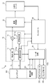
- the fluorescence detection apparatus 1 includes a signal processing circuit 10, an image processing unit 20, an input / output unit 30, a controller 40, and a servo.
- a circuit 50 and a thread motor 240 are provided.
- the signal operation circuit 300 in FIG. 8 is provided in the fluorescence detection pickup 200.
- the signal processing circuit 10 of the fluorescence detection apparatus 1 processes the fluorescence signal FL and the reproduction RF signal RF output from the fluorescence detection pickup 200.
- the fluorescence signal is output from the fluorescence detector 211 in FIG. 7, and the reproduction RF signal RF is output from the adder 307 in FIG.
- the signal processing circuit 10 includes a signal detection unit 11, a signal reproduction unit 12, a cutout unit 13, and a superposition unit 14.
- the signal detection unit 11 and the signal reproduction unit 12 constitute a signal acquisition unit 11a.
- the signal detection unit 11 processes the reproduction RF signal RF input from the fluorescence detection pickup 200, detects various signals shown in FIG. 6A, and sends the detected signals to the signal reproduction unit 12, the cutout unit 13, and the controller 40. Output.
- the signal reproduction unit 12 reproduces the signals in the fields F3 and F8 input from the signal detection unit 11, that is, the signals in the header areas HE0 to HE2 and the footer areas FT0 to FT2, and acquires an address signal.
- the signal reproducing unit 12 outputs the acquired address signal to the superimposing unit 14.
- the cutout unit 13 converts each sample value obtained by sampling the fluorescence signal input from the fluorescence detection pickup 200 with a sampling clock of a predetermined period into a digital signal and outputs the digital signal to the superimposition unit 14.
- the cutout unit 13 ends the sampling of the fluorescence signal FLd in response to detection of the start signal V3 (see FIG. 5A) by the signal detection unit 11.
- the sample storage disk 100 is rotated at a different angular velocity for each zone. Accordingly, the time during which the track portion Ta is scanned with the laser light varies from zone to zone. For this reason, when a fluorescence signal is cut out with a timing signal having the same period for each zone, the number of cut out signal groups differs for each zone.
- the period of the sampling clock in the cutout unit 13 is adjusted so that the same number of signal groups are cut out from the track portion Ta of each zone. Thereby, in each zone, the fluorescence signal FL is cut out at substantially the same angular interval.
- the superimposing unit 14 adds the address signal input from the signal reproducing unit 12 to the fluorescence signal acquired by the clipping unit 13 and outputs the signal to the image processing unit 20.
- the image processing unit 20 connects the input fluorescent signals to generate a fluorescent image for each of the areas A0 to A8.
- the image processing unit 20 performs image processing on the fluorescent image, counts the number of fluorescent bright spots, and calculates the infection rate of malaria in the red blood cells RC. These fluorescent images, count values, infection rates, and the like are output from the image processing unit 20 to the input / output unit 30 as needed.
- the controller 40 controls the servo circuit 50 and the signal processing circuit 10 so that the period from the start signal V3 in which the address signal has changed to the end signal Vs is scanned again with the laser light and the fluorescent signal is extracted.
- the input / output unit 30 includes input devices such as a keyboard, a mouse, and a touch panel, and output devices such as a monitor and a speaker.
- An instruction for starting fluorescence detection is input via the input / output unit 30.
- the fluorescence image, the number of bright spots, the infection rate of malaria, and the like are displayed on the input / output unit 30.
- a method of obtaining a fluorescent image of the entire flow path by staining the cells to be detected with a fluorescent dye and storing them in the flow path can be used.
- the presence / absence and number of detection target cells can be acquired by analyzing the acquired fluorescence image, and based on this, the infection rate of pathogenic bacteria and the like can be acquired. It is also possible to display the acquired fluorescence image as appropriate and visually confirm the occurrence of fluorescence.
- the controller 40 includes a processing circuit such as a CPU (Central Processing Unit) and a memory such as a ROM (Read Only Memory) and a RAM (Random Access Memory), and controls each unit according to a program stored in the memory.
- a processing circuit such as a CPU (Central Processing Unit) and a memory such as a ROM (Read Only Memory) and a RAM (Random Access Memory), and controls each unit according to a program stored in the memory.
- the servo circuit 50 controls the objective lens actuator 207 based on the focus error signal FE and the tracking error signal TE generated by the signal calculation circuit 300 in FIG.
- the servo circuit 50 controls the spindle motor 220 so that the zones Z0 to Zn shown in FIG. 3B are scanned by the beam spot B1 at the angular velocity set in each zone.
- the servo circuit 50 is a thread for sending the fluorescence detection pickup 200 in the disk radial direction Dr of the sample storage disk 100 so that the beam spot B1 can be scanned from the outermost position to the innermost position of the track 102c.
- the motor 240 is controlled.
- the servo circuit 50, the fluorescence detection pickup 200, the spindle motor 220, and the sled motor 240 constitute a scanning unit 1200 that irradiates the sample storage disk 100 with light and scans the sample storage disk 100 in the scanning direction Ds.
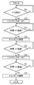
- FIG. 10A is a flowchart showing an address signal acquisition process.
- the signal reproduction unit 12 acquires a signal in the header region HE1 from the signal detection unit 11 (S11), and applies an error correction signal to the address signal in the acquired signal to perform error correction processing (S12). If the error correction process is appropriate (S13: YES), the signal reproduction unit 12 does not perform the address signal reproduction process on the header region HE2, and uses the address signal acquired by the error correction process in the field F3 (FIG. 5A). Reference) address signal (S14), and the process ends. On the other hand, if the error correction processing is not appropriate (S13: NO), the signal reproduction unit 12 further acquires a signal in the header area HE2 (S15), and applies an error correction signal to the address signal in the acquired signal to generate an error. Correction processing is performed (S16). If the error correction process is appropriate (S17: YES), the signal reproduction unit 12 acquires the address signal acquired by the error correction process as the address signal of the field F3 (see FIG. 5A) (S18), and performs the process. finish.
- steps S12 and S16 error detection processing and error correction processing are performed using the error correction signals included in the header areas HE1 and HE2. If no error is detected in the address signal, it is determined that the address signals included in the header areas HE1 and HE2 are appropriate. When an error is detected, an error bit in the address signal is extracted by an operation using the error correction signal, and the error bit is corrected. If the determination in step S17 is NO, the controller 40 scans the track portion Ta again.
- the address signal acquisition process for the footer areas FT1 and FT2 is performed in the same manner as the address signal acquisition process for the header areas HE1 and HE2 shown in FIG. 10A. That is, in the address signal acquisition process for the footer areas FT1 and FT2, the processing steps S11 and S12 for acquiring the signals of the header areas HE1 and HE2 in FIG. 10A are replaced with processes for acquiring the signals of the footer areas FT1 and FT2, respectively. It is done.
- the address signal since the address signal is recorded in each of the header areas HE1 and HE2, the address signal can be acquired from the header area HE2 even when the address signal cannot be properly read from the header area HE1. .
- FIG. 10B is a flowchart showing tracking control.
- the servo circuit 50 maintains the tracking servo signal at the previous signal value (S22) and waits for the time Ts1 to elapse. (S23).
- the time Ts1 is set to a time required for the beam spot B1 to pass through the start end of the field F5. Since the starting end of the field F5 is located at the boundary (end) of the sample storage unit 101b, the reflectance of the laser beam changes greatly at this position, and the tracking error signal is easily disturbed. When the tracking error signal is disturbed, there is a possibility that the scanning position of the beam spot B1 is shifted from the target track to an adjacent track or the like.
- the tracking servo signal is maintained at the previous signal value until the beam spot B1 passes through the beginning of the field F5, that is, until the time Ts1 elapses (S22). It prevents it from coming off. Thereby, the track 102c can be stably scanned with the laser beam.
- the servo circuit 50 resumes tracking servo (S24). Thereafter, when the time Ts2 elapses (S25: YES), the servo circuit 50 again maintains the tracking servo signal at the previous signal value (S26), and waits for the time Ts3 to elapse (S27). When the time Ts3 has elapsed (S27: YES), the servo circuit 50 resumes tracking servo (S28).
- the time Ts2 is set to the time required for the beam spot B1 to reach the position immediately before the end of the field F5.
- the time Ts3 is set to the time required for the beam spot B1 to pass through the end of the field F5 from the position immediately before the end of the field F5.
- the purpose of maintaining the tracking servo signal near the end of the field F5 in the processing of steps S25 to S27 and the effect thereof are the purpose of maintaining the tracking servo signal near the start of the field F5 in the processing of steps S22 to S23 and The effect is the same. That is, this process also takes into consideration that the reflectance of the laser beam changes greatly at the end of the field F5 and the tracking error signal is likely to be greatly disturbed. By these processes, the track 102c can be stably scanned, and as a result, the fluorescence signal extraction process can be smoothly advanced.
- step S27 it is determined that the time Ts3 to reach the end of the field F5 has elapsed, but a predetermined signal is further recorded before the end of the field F5, and the process is performed by detecting this signal. You may move to.
- FIG. 11A is a flowchart showing a cutting process for cutting out a fluorescent signal.
- the extraction unit 13 starts extraction (sampling) of the fluorescence signal (S32). Thereafter, when the signal detection unit 11 detects the end signal Vs (see FIG. 5A) (S33: YES), the extraction unit 13 ends the extraction (sampling) of the fluorescence signal (S34).
- the controller 40 may control the cutout unit 13 so that the cutout unit 13 starts to cut out the fluorescence signal later.
- the extraction of the fluorescence signal ends in response to the detection of the end signal Vs.
- the extraction unit 13 outputs the fluorescence signal at the timing immediately before the end of the field F5.
- the controller 40 may control the cutting unit 13 so that the cutting is finished.
- FIG. 11B is a flowchart showing invalidation processing for invalidating the cut-out signal.
- the controller 40 acquires the address signal reproduced from the header areas HE1 and HE2 while scanning one track portion Ta (S41), and acquires the address signal reproduced from the footer areas FT1 and FT2 (S42). .
- the controller 40 determines whether or not the two address signals acquired in this way match (S43). If the two address signals do not match (S43: No), the controller 40 invalidates the fluorescence signal cut out from the track portion Ta (S44), scans the track portion Ta again with laser light, and outputs the fluorescence signal.
- the cutting unit 13 is controlled so as to cut out (S45). When the two address signals match (S43: Yes), the controller 40 ends the process without invalidating the fluorescent signal cut out from the track portion Ta.
- the laser beam spot B1 may have moved out of the groove 111 and moved to another groove while scanning the groove 111 overlapping the sample storage unit 101b. .
- the fluorescence signal cut out in the meantime is acquired across two track portions, and is not a fluorescence signal acquired from one track portion.
- the fluorescence detection apparatus 1 while the process of FIG. 11B is executed and the groove 111 that overlaps the sample storage unit 101b is scanned, the beam spot B1 of the laser beam is separated from the groove 111 and moves to another groove. If there is a possibility of movement, the fluorescence signal acquired during that time is invalidated and the fluorescence signal is cut out again. Thereby, a fluorescence signal is appropriately acquired from one track portion Ta.
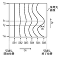
- FIG. 12 is a diagram for explaining the fluorescence signal cutting process.
- the cutout unit 13 samples the fluorescence signal output from the fluorescence detection pickup 200 in synchronization with the sampling clock Sck with a certain period while the laser beam scans the field F5, and acquires the sample value at each timing.
- FIG. 12 schematically shows the sampling clock Sck and signals cut out from one group of track portions Ta (track numbers T0 to Tm) included in the same area in the same zone.
- k signals SP1 to SPk are obtained from one track portion Ta.
- red blood cells RC infected with malaria are present in the sample at the timing when the signal SP5 is scanned while the track portion Ta of the track number T1 is scanned with the laser beam.
- the sampling value of the signal SP5 of the track number T1 is higher than the other signals SP1 to SP4 and SP6 to SPk of the track number T1 and the signals SP1 to SPk of the other tracks (track numbers T0, T2 to Tm).
- Sample values of signals around signal SP5 are larger than those of signals SP5 of signals SP4 to SP6 and the surrounding signals. It is high.
- the higher the sample value the higher the hatching density.
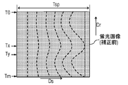
- the image processing unit 20 in FIG. 9 performs the scanning order and track number of signals of one group of track portions Ta included in the same area in the same zone based on the signal and address signal input from the superimposing unit 14. Are arranged in this order to generate a fluorescence image showing one sample storage unit 101b.
- the image processing unit 20 analyzes the fluorescence image thus generated, counts the number of fluorescent bright spots, that is, the number of red blood cells RC infected with malaria, and based on the number, malaria of red blood cells RC contained in the sample 100Sa. Calculate the infection rate.
- the image processing unit 20 outputs the acquired count value and infection rate to the input / output unit 30 together with the fluorescent image. As a result, the fluorescence image, the number of detected malaria, the malaria infection rate, and the like are displayed on the input / output unit 30.
- the sample container 101b is arranged so that two boundaries (ends) in the disk circumferential direction Dc extend radially from the disk center Pc. For this reason, when the sample storage disk 100 is rotated at a constant angular velocity, the range of the sample storage portion 101b is scanned when a laser beam is used to scan an arbitrary track portion Ta that overlaps one sample storage portion 101b as viewed from above. The period of time is substantially constant. Thereby, in the fluorescence detection device 1 as described above, the start signal V3 and the end signal Vs (see FIG.
- the fluorescent signal is sampled and cut out at a predetermined interval. Accordingly, a series of fluorescent image fragments along one track portion Ta can be acquired from the sample 100Sa accommodated in the sample accommodating portion 101b. The fragments acquired in this manner are joined together as shown in FIG. 12, whereby a fluorescence image of the entire sample storage unit 101b can be acquired.
- a header region HE1, HE2 and a footer region FT1, FT2 are provided upstream and downstream of the sample storage portion 101b in the scanning direction of the track 102c, respectively. Is set.
- address signals having the same contents are recorded in the header areas HE1 and HE2 and the footer areas FT1 and FT2, respectively.
- the sample storage disk 100 is divided into areas A0 to A8 in the disk circumferential direction Dc.
- Two boundaries (ends) in the disk circumferential direction Dc of each area extend radially from the disk center Pc in the disk radial direction Dr. That is, the two boundaries B01 and B80 aligned in the disk circumferential direction Dc of the area A0 extend in the disk radial direction Dr away from the disk center Pc.
- the two boundaries B01 and B12 aligned in the disk circumferential direction Dc of the area A1 extend in the disk radial direction Dr away from the disk center Pc.
- Two boundaries B12 and B23 aligned in the disk circumferential direction Dc of the area A2 extend in the disk radial direction Dr away from the disk center Pc.
- Two boundaries B23 and B34 aligned in the disk circumferential direction Dc of the area A3 extend in the disk radial direction Dr away from the disk center Pc.
- Two boundaries B34 and B45 aligned in the disk circumferential direction Dc of the area A4 extend in the disk radial direction Dr away from the disk center Pc.
- Two boundaries B45 and B56 aligned in the disk circumferential direction Dc of the area A5 extend in the disk radial direction Dr away from the disk center Pc.
- Two boundaries B56 and B67 aligned in the disk circumferential direction Dc of the area A6 extend in the disk radial direction Dr away from the disk center Pc.
- Two boundaries B67 and B78 aligned in the disk circumferential direction Dc of the area A7 extend in the disk radial direction Dr away from the disk center Pc.
- Two boundaries B78 and B80 arranged in the disk circumferential direction Dc of the area A8 extend in the disk radial direction Dr away from the disk center Pc.
- Sample storage portions 101b are arranged in the areas A0 to A8, respectively, and the track portion Ta included in each area straddles the sample storage portion 101b. Thereby, when the sample storage disk 100 is rotated at a constant angular velocity, the track portions Ta included in each area are all scanned with the same time length. Therefore, the same signal format can be applied uniformly to all track portions Ta.
- the angular ranges of the areas A0 to A8 in the disk circumferential direction Dc with respect to the disk center Pc are set to be equal to each other. Therefore, the fluorescence signal can be cut out from all the areas A0 to A8 by the same processing.
- the sample storage disk 100 is divided into a plurality of zones Z0 to Zn in the disk radial direction Dr, and signals are recorded at a constant angular velocity in the track portion Ta of each zone.
- the angular velocities of the zones Z0 to Zn are set so that the linear velocities of the track portions Ta at the center position in the disk radial direction Dr of each zone are the same.
- the difference between the linear velocity on the inner periphery side of the disc and the linear velocity on the outer periphery side of the disc can be suppressed.
- the track portion Ta includes a signal indicating a zone including the track portion Ta, a signal indicating the position (track number) of the track portion in the disk radial direction Dr in the zone, A signal indicating the position (area) of the track portion Ta in the disk circumferential direction Dc is recorded as an address signal.
- the sample storage disk 100 that stores the sample 100Sa is disposed above the substrate 102, the track 102c formed on the upper surface 102p of the substrate 102 so as to turn around the disk center Pc, and the track 102c. And one or more sample storage portions 101b for storing the sample 100Sa.
- the track 102c is configured to be scanned in the scanning direction Ds.
- Each of the plurality of track portions Ta straddling each sample storage portion 101b of the one or more sample storage portions 101b in the track 102c is upstream of each sample storage portion 101b in the scanning direction Ds of each track portion Ta.
- An address signal indicating the position of the track portion Ta is recorded.
- Another address signal indicating the position of each track portion Ta is recorded on the downstream side of each sample storage portion 101b in the scanning direction Ds of each track portion Ta.
- a plurality of start signals V3 indicating the start of the respective sample storage portions 101b in the scanning direction Ds are upstream from the respective sample storage portions 101b in the scanning direction Ds of the plurality of track portions Ta. May be recorded so as to be aligned with each other.
- a plurality of end signals Vs indicating the end of each sample storage portion 101b in the scanning direction Ds are separated from the disc center Pc. It may be recorded so as to be aligned in the direction Dr.
- the area of the sample storage disk (track area 102a) on which the track 102c is formed extends in the disk circumferential direction Dc perpendicular to the plurality of disk radial directions Dr at a plurality of boundaries extending in the plurality of disk radial directions Dr away from the disk center Pc. It may be divided into a plurality of arranged areas A0 to A8. A plurality of sample storage portions 101b are respectively arranged in the plurality of areas A0 to A8.
- the plurality of areas A0 to A8 may be arranged within the same angular range from the disc center Pc.
- the portions of the plurality of track portions Ta that overlap one or more sample storage portions 101b as viewed from above may be monotonously extended without signals being recorded.
- the synchronization adjustment signals may be recorded in at least one of the portions of the plurality of track portions Ta that overlap one or more sample storage portions 101b as viewed from above.
- the plurality of track portions Ta may be arranged in the disc radial direction Dr away from the disc center Pc. Even if the plurality of signals En indicating the start ends SP at which the plurality of track portions Ta start in the scanning direction Ds are arranged in another disc radial direction Dr away from the disc center Pc, they are recorded at the start ends SP of the plurality of track portions Ta. Good. A plurality of signals En indicating end EPs at which the plurality of track portions Ta end in the scanning direction Ds are recorded at the end EPs of the plurality of track portions Ta so as to be arranged in another disc radial direction Dr away from the disc center Pc. Also good.
- the sample storage disk 100 may be divided into a plurality of zones Z0 to Zn along the disk radial direction Dr away from the disk center Pc.
- a plurality of groups of track portions Ta among the plurality of track portions Ta are respectively arranged in the plurality of zones Z0 to Zn.
- a signal may be recorded at a constant angular velocity on each track portion Ta of the plurality of track portions.
- the constant angular velocity is set so that the linear velocity of the track portion Ta at the center position in the disk radial direction Dr of the track portions Ta of each group becomes a predetermined linear velocity in the track portions Ta of the plurality of groups. It may be.
- Each of the two address signals includes a signal indicating a zone including each track portion Ta among the plurality of zones Z0 to Zn, and a signal indicating a position of each track portion Ta in the zone in the disk radial direction Dr. , And a signal indicating the position of each track portion Ta in the disk circumferential direction Dc perpendicular to the disk radial direction Dr and surrounding the disk center Pc.
- the address signal is recorded by a pit row composed of a plurality of pits 113 formed on the track 102c.
- the two boundaries arranged in the disk circumferential direction Dc surrounding the disk center Pc of the one or more sample storage units 100b may extend radially from the disk center Oc.
- the fluorescence detection apparatus 1 includes a scanning unit 1200 that irradiates the sample storage disk 100 with light and scans the sample storage disk 100 in the scanning direction Ds, and a light detection that outputs a detection signal according to the light reflected by the sample storage disk 100.
- a signal acquisition unit 11a that operates according to the detection signal
- a fluorescence detector 211 that outputs a fluorescence signal corresponding to the fluorescence generated from the sample 100Sa accommodated in the sample accommodation unit 101b by the irradiated light
- a cutout unit 13 that samples and cuts out the fluorescent signal
- a controller 40 that controls processing of the cut out fluorescent signal are provided.
- the signal acquisition unit 11a acquires two address signals based on the signal output from the photodetector 210. Based on the two address signals acquired by the signal acquisition unit 11a, the controller 40 controls the above processing on the cut-out fluorescence signal.
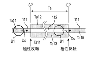
- FIG. 13 is a diagram in which grooves and lands in each zone of the sample storage disk 100a according to the second embodiment are developed in a straight line.
- the same reference numerals are assigned to the same parts as those of the sample storage disk 100 in the first embodiment shown in FIGS. 1A to 6A.
- the groove 111 extends spirally from the outermost periphery to the innermost periphery.
- the groove 111 and the land 112 are alternately replaced each time the area is switched in the disk circumferential direction Dc. Yes.
- the track area 102a of the sample storage disk 100a is divided into nine areas A0 to A8 in the disk circumferential direction Dc. Therefore, when the track 102 c starting from the groove 111 makes one round, the next one track 102 c starts from the land 112.
- the groove 111 and the land 112 are alternately repeated in the disk radial direction Dr.
- the number of track portions Ta of each zone is set so that the track 102c of the track number T0 of all zones starts from the groove 111.
- the number of tracks 102c (track portions Ta) included in one zone is, for example, 1600, which is twice that of the sample storage disk 100 in the first embodiment.
- the sample storage disk 100 In the sample storage disk 100 according to the first embodiment, only the groove 111 is scanned with laser light.
- the sample storage disk 100a according to the second embodiment as shown in FIG. 13, since the track 102c is formed by alternately repeating the groove 111 and the land 112, the groove 111 and the land 112 are alternately scanned in the disk circumferential direction Dc. Is done. Therefore, the land 112 that is not scanned by the sample storage disk 100 in the first embodiment is also scanned by the laser beam in the sample storage disk 100a in the second embodiment. For this reason, the number of areas scanned by the laser beam of the sample storage disk 100a in the second embodiment is twice that of the sample storage disk 100 in the first embodiment, and the scanning density of the sample storage section 101b is also doubled. It becomes.
- the density at which the fluorescence signal is cut out in the sample storage disk 100a in the second embodiment is twice that in the sample storage disk 100 in the first embodiment, and a higher-definition fluorescent image is obtained with the sample storage disk 100a in the second embodiment. It is done.
- FIG. 14A shows the format of each field set in the track portion Ta of one area of the sample storage disk 100a according to the second embodiment.
- a signal is recorded only on the track portion Ta (Ta12 to Ta15) made of the groove 111, and the signal is recorded on the track portion Ta (Ta11) made of the land 112. Is not recorded.
- the format of the signal recorded on the track portion Ta (Ta11) made of the groove 111 is the same as the format of the sample storage disk 100 in the first embodiment shown in FIG. 5A.
- the reason why the signal is not recorded in the track portion Ta (Ta11) including the land 112 is as follows. That is, when a signal is recorded on the track portion Ta composed of the lands 112, when the signal is read by scanning the track portion Ta composed of the grooves 111 with the beam spot B1, the track portion Ta composed of the land 112 adjacent thereto is simultaneously read. The beam spot B1 is applied, and light is modulated by the track portion Ta made of the land 112. For this reason, the reproduction RF signal RF from the track portion Ta composed of the groove 111 to be originally read is disturbed, and the signal cannot be acquired properly. For this reason, in the sample storage disk 100a according to the second embodiment, a signal is recorded only on the track portion Ta made of the groove 111.
- the fields F1, F4, F6, and F9 are Each is aligned in the disk radial direction Dr.
- the same signal is recorded in each of the track portions Ta (Ta12 and Ta13) including the grooves 111 arranged in the disk radial direction Dr.
- the portions on both sides of the beam spot B1 in the disc radial direction Dr become adjacent two track portions Ta (Ta12, Ta13). Therefore, the signals are modulated by signals recorded in the fields F1, F4, F6, and F9 of the track portion Ta (Ta12, Ta13). Therefore, even when the track portion Ta (Ta11) made of the lands 112 is scanned with laser light, the track portion Ta (Ta12, Ta13) adjacent to the track portion Ta (Ta11) in the disk radial direction Dr. The signals recorded in the fields F1, F4, F6, and F9 can be properly read.
- the signals V3 and Vs are appropriately transmitted from the track portions Ta (Ta12 and Ta13) adjacent to the disk radial direction Dr. To be acquired. Therefore, even when the track portion Ta (Ta11) made of the land 112 is scanned with the laser beam, the control shown in FIGS. 10B and 11A is performed when the track portion Ta (Ta12 to Ta15) made of the groove 111 is scanned with the laser beam. Can be done as well.
- signals recorded in the fields F3 and F8 shown in FIG. 14A that is, address signals
- the track portion Ta (Ta11) formed of the lands 112 is scanned with laser light
- the address signal cannot be properly acquired from F3 and F8.
- the track portion Ta (Ta11) including the land 112 is adjacent to the track portion Ta (Ta14) adjacent to the upstream side in the scanning direction Ds with respect to the track portion Ta (Ta11).
- Address signals acquired from the footer areas FT1 and FT2 and addresses acquired from the header areas HE1 and HE2 of the track part Ta (Ta15) adjacent downstream in the scanning direction Ds with respect to the track part Ta (Ta11). Based on the signal, the processing of FIG. 11B is performed.
- step S41 an address signal is acquired from the header areas HE1 and HE2 of the track portion Ta (Ta15) on the downstream side of the track portion Ta (Ta11) including the land 112.
- step S42 the track portion including the land 112 is obtained.
- Address signals are acquired from the footer areas FT1 and FT2 of the track portion Ta (Ta14) on the upstream side of Ta (Ta11).
- step S43 it is determined whether or not the relationship between both address signals is appropriate. That is, when the zone numbers of both address signals match, the track numbers of both address signals match, and the area numbers of both address signals have continuity, it is determined that the relationship between both address signals is appropriate.
- the area numbers of both address signals have continuity means that the area number acquired from the address signal recorded in the track portion Ta15 and the area number acquired from the address signal recorded in the track portion Ta14 are three consecutive numbers. This means that the area number relationship of the areas at both ends of the area is satisfied. For example, when the track portion Ta14, the track portion Ta11, and the track portion Ta15 are respectively arranged in areas with consecutive area numbers increased by 1 in this order, the address signal recorded in the track portion Ta11. When the difference between the area number acquired from the above and the area number acquired from the address signal recorded in the track portion Ta15 is 2, the area numbers of both address signals have continuity.
- the relationship between both address signals is not appropriate Determined.
- the processing of steps S44 and S45 is performed.
- the fluorescence signal is validated and the processing shown in FIG. 11B is performed. Finish.
- the region of the beam spot B1 modulated by the groove 111 is the beam spot B1.
- Dr the polarity of the tracking error signal TE is reversed every time the position where the beam spot B1 scans passes the boundary between the groove 111 and the land 112.
- FIG. 14B is a diagram illustrating a polarity inversion unit 51 that inverts the polarity of the tracking error signal TE according to the second embodiment.
- FIG. 14C is a diagram schematically illustrating the timing of reversing the scanning of the beam spot B1 and the polarity of the tracking error signal TE related to the sample storage disk 100a in the second embodiment.
- the polarity reversing unit 51 is provided in the servo circuit 50 shown in FIG.
- the signal detector 11 is provided in the signal processing circuit 10 shown in FIG.
- the polarity inversion unit 51 inverts the polarity of the tracking error signal TE and supplies it to the circuit unit for tracking servo.
- the beam spot B1 moves from the track portion Ta (Ta14) made of the groove 111 to the track portion Ta (Ta11) made of the land 112
- the track portion Ta (Ta14) and the track portion are moved.
- the polarity of the tracking error signal TE is inverted at the timing of passing through the boundary with Ta (Ta11).
- the beam spot B1 can be positioned on the track 102c without deviation even when the scanning position shifts from the groove 111 to the land 112.
- the beam spot B1 moves from the track portion Ta (Ta11) made of the land 112 to the track portion Ta (Ta15) made of the groove 111, the beam spot B1 passes through the boundary with the track portion Ta (Ta15) that becomes the track portion Ta (Ta11).
- the polarity of the tracking error signal TE returns to the original and is output from the polarity inverting unit 51 with the same polarity.
- the beam spot B1 can be positioned on the track 102c without deviation even when the scanning position shifts from the land 112 to the groove 111. Therefore, it is possible to stably extract the fluorescence signal.
- the same effect as that of the sample storage disk 100 in the first embodiment can be achieved.
- the area of the land 112 is also scanned with the laser light. Therefore, the number of areas scanned with the laser light is equal to the number of the areas that are scanned with the laser light.
- the scanning density for the sample container 101b is also doubled. Therefore, in the sample storage disk 100a in the second embodiment, the density at which the fluorescence signal is cut out is twice that of the sample storage disk 100 in the first embodiment, and a higher-definition fluorescent image is obtained.
- FIG. 14D schematically shows the structure of the groove 111, the land 112, and the pit 113 of another sample storage disk 100b according to the second embodiment. 14D, the same reference numerals are assigned to the same portions as those of the sample storage disk 100 according to Embodiment 1 shown in FIG. 2 showing the structure of the sample storage disk 100a.
- the land 102 may constitute the track 102c. That is, by forming the pit 113 on the land 112, the signal of each field shown in FIG. 5A may be recorded. In this case, the pit 113 is not formed in the groove 111 and extends monotonously and flatly.
- a signal is recorded on the track 102c in a pit row including a plurality of pits 113 formed on one of the groove 111 and the land 112.
- the light is not modulated by a different signal from a track adjacent to the track, and the signal can be read appropriately from the track.
- the track 102c is configured so that the groove 111 and the land 112 are switched each time the areas A0 to A8 are switched. For this reason, compared with the case where the track 102c is constituted by the series of grooves 111, the sample storage portion 101b can be scanned with a fine pitch in the disk radial direction Dr. In addition, a signal is recorded by the pit 113 only in the groove 111 of the groove 111 and the land 112. For this reason, when the groove 111 is scanned with the beam spot B1, the beam spot B1 is not modulated by a different signal of the adjacent land 112, and the signal can be appropriately read from the track 102c.
- the sample storage unit 101b is configured such that two boundaries in the disk circumferential direction Dc extend radially from the disk center Pc, respectively, when the sample storage disk 100a (100b) is rotated at a constant angular velocity, 1 Regardless of which track 102c that overlaps one sample storage unit 101b is scanned with laser light, the period during which the range of the sample storage unit 101b is scanned is substantially constant. Therefore, by extracting the fluorescence signal by the process of FIG. 11A of the first embodiment, a signal group of a series of fluorescence images along one track 102c can be acquired from the sample 100Sa accommodated in the sample accommodating portion 101b. it can. By connecting the acquired signal group in the disk circumferential direction Dc and the disk radial direction Dr, a fluorescence image of the entire sample storage unit 101b can be acquired.
- a signal En for recording that the track structure is switched from the groove 111 to the land 112 is recorded at the end EP of the groove 111 in the scanning direction Ds. Therefore, with the configuration of FIG. 14B, the track 102c can be smoothly scanned with the beam spot B1 by inverting the polarity of the tracking error signal TE in accordance with the detection of the signal En.
- the angle ranges of the areas A0 to A8 centered on the disc center Pc in the disc circumferential direction Dc are set to be equal to each other. Therefore, the fluorescence signal can be cut out from all the areas A0 to A8 by the same processing.
- the groove 111 includes a start signal V3 indicating the start of the sample storage unit 101b on the upstream side and the downstream side of the sample storage unit 101b in the scanning direction Ds, and the sample storage unit.
- An end signal Vs indicating the end of 101b is recorded.
- Each pit 113 for recording the start signal V3 included in the same area is formed to be aligned radially from the disc center Pc.
- Each pit for recording the end signal Vs included in the same area is formed so as to be aligned radially from the disc center Pc.
- the substrate 102 includes lands 112 that constitute the upper surface 102 p of the substrate 102, and grooves 111 that are provided on the upper surface 102 p and are connected to the lands 112.
- the track 102c is provided in the land 112 and the groove 111 so as to be alternately switched between the groove 111 and the land 112 at a plurality of boundaries.
- a signal is recorded on the track 102c in a pit row composed of a plurality of pits 113 formed on one of the groove 111 and the land 112.
- FIG. 15A shows the format of each field set in the track portion Ta (groove 111) of one area of the sample storage disk 100c in the third embodiment.
- FIG. 15B shows a part of the signal format of the sample storage disk 100c in the third embodiment, and particularly shows the field F5.
- FIG. 15C is a diagram schematically illustrating the configuration of the synchronization adjustment pit SB1 that constitutes the synchronization adjustment signal recorded on the sample storage disk 100c according to the third embodiment.
- 15A to 15C the same reference numerals are assigned to the same portions as those of the sample storage disk 100 in the first embodiment shown in FIGS. 1A to 6B.
- the pit 113 is not formed in the groove 111 of the field F5.
- the pit 113 for synchronization adjustment is formed in the groove 111 of the field F5.
- the fluorescence signal is sampled according to the sampling clock Sck having a constant period, and the signals SP1 to SPk are acquired.
- the sample storage disk 100 is rotated at a constant angular velocity for each zone as described above.
- the angular velocity of the rotation of the sample storage disk 100 fluctuates and uneven rotation occurs.
- the rotation unevenness may cause distortion in the scanning direction Ds in the signal of one column of each track, and as a result, the accuracy of the fluorescent image may decrease. .
- the pit 113 for synchronization adjustment is formed in the groove 111 of the field F5, and the distortion generated in the fluorescent image is corrected using the pit 113.
- synchronization adjustment pits SB1 to SB6 are arranged at a constant angular interval with respect to the disk center Pc.
- the synchronization adjustment pits SB1 are aligned in the disc radial direction Dr.
- the other synchronization adjustment pits SB2 to SB6 are similarly configured. That is, both ends of each pit 113 of the synchronization adjustment pits SB2 to SB6 are also aligned in the disk radial direction Dr in all zones and tracks.
- the field F5 overlaps the sample storage portion 101b in the entire length.
- both ends of the field F5 coincide with two boundaries (ends) arranged in the disk circumferential direction Dc of the sample storage unit 101b.
- No signal is recorded other than the synchronization adjustment pits SB1 to SB6 in the portion of the track portion Ta that overlaps the sample storage portion 101b, and the portion other than the portion where the synchronization adjustment pits SB1 to SB6 are recorded is a monotonically extending groove. Only 111 is formed.
- the synchronization adjustment pit SB1 includes a plurality of pits 113.
- five pits 113 are shown as the synchronization adjustment pits SB1, but actually, the synchronization adjustment pits SB1 are composed of about several tens of pits 113.
- the synchronization adjustment pit SB1 is formed of a combination of a pit length and a land length different from any other pit recorded in the groove 111.
- both ends of each pit 113 of the synchronization adjustment pit SB1 are aligned in the disc radial direction Dr in all zones and tracks.
- FIG. 15C shows the configuration of the synchronization adjustment pit SB1, but the synchronization adjustment pits SB2 to SB6 have the same contents and configuration as the synchronization adjustment pit SB1. That is, both ends of each pit 113 of the synchronization adjustment pits SB2 to SB6 are also aligned in the disk radial direction Dr in all zones and tracks.
- the beam spot B1 is the land 112 portion in the signal format of the second embodiment.
- both ends of the beam spot B1 are simultaneously applied to the pits 113 of the synchronization adjustment pits SB2 to SB6 formed in the groove 111 adjacent to the land 112 in the disk radial direction Dr. It can be detected properly. Therefore, even when the field F5 of the land 112 is scanned with the beam spot B1, the synchronization adjustment pits SB1 to SB6 can be properly detected.
- a signal output from the photodetector 210 is combined with a sampled signal in the same manner as a fluorescent image to obtain one signal light image, and from the acquired signal light image
- the synchronization adjustment pit SB1 can be detected by image processing.
- FIG. 16 is a configuration diagram of the fluorescence detection device 1a used together with the sample storage disk 100c.
- the fluorescence detection apparatus 1a illustrated in FIG. 16 further includes a cutout unit 15 and a superimposition unit 16, and an address signal is superimposed on a signal obtained by sampling the signal output from the photodetector 210 and output to the image processing unit 20.
- the image processing unit 20 connects the input signals to generate a signal light image corresponding to the fluorescent image.
- the image processing unit 20 processes the generated signal light image to detect the synchronization adjustment pits SB1 to SB6 of the track portion Ta on the signal light image.
- the image of one synchronization adjustment pit has a remarkably high correlation coefficient at a position aligned with the reference image of the synchronization adjustment pit. If the reference image is shifted in the scanning direction Ds, the correlation coefficient is adjusted to be remarkably low at any shift position.
- the synchronization adjustment pits SB1 to SB6 are formed of pit patterns that satisfy such a correlation with the reference image in detection by image processing.
- FIG. 17A schematically shows a detection position where the synchronization adjustment pits SB1 to SB6 are detected on the signal light image obtained from the sample storage disk 100c by a solid line.
- the shift amount between the track portions Ta of the synchronization adjustment pits SB1 to SB6 gradually increases as the signal proceeds from the cutout start position to the downstream side in the scanning direction Ds.
- the shift amounts of the synchronization adjustment pits SB1 to SB6 between the track portions Ta adjacent to each other in the disk radial direction Dr are relative to the position in the scanning direction Ds from the position where the cutting starts. Increases monotonically and increases linearly.
- the shift amount of each of the synchronization adjustment pits SB1 to SB6 between the track portions Ta periodically repeats the maximum value and the minimum value in 8 to 10 track portions, and the shift amount Remains within the range of 100 pixels.
- FIG. 17A schematically shows that the detection positions of the synchronization adjustment pits SB1 to SB6 change due to the rotation unevenness of the sample storage disk 100 for convenience of explanation.
- the shift amounts of the synchronization adjustment pits SB1 to SB6 between the track portions Ta adjacent to each other in the disk radial direction Dr are periodically set to the maximum value every 8 to 10 track portions. It fluctuates periodically to repeat the minimum value.
- the 16 corrects the fluorescent image based on the distribution of the synchronization adjustment pits SB1 to SB6 on the signal light image shown in FIG. 17A. Specifically, the image processing unit 20 corrects the fluorescence image so that the fluorescence signals cut out at the positions of the synchronization adjustment pits SB1 to SB6 on the fluorescence image are arranged in a line in the disk radial direction Dr. .
- FIG. 17B and FIG. 17C schematically show fluorescent image correction processing. Specifically, FIG. 17B shows a fluorescence image before correction by the signal light image, and FIG. 17C shows a fluorescence image after correction by the signal light image. For convenience, FIGS. 17B and 17C show the detection positions of the synchronization adjustment pits SB1 to SB6 by broken lines.
- the synchronization adjustment pit SB6 is located on the most downstream side in the scanning direction Ds.
- the image processing unit 20 uses, as a reference signal group, a signal group composed of signals of the track portion Ta of the track number Tx whose detection position of the synchronization adjustment pit SB6 is the most downstream in the scanning direction Ds among the track numbers T0 to Tm. Decide.
- a signal group (correction) composed of signals of the track portion Ta of other track numbers Ty (y is an arbitrary integer satisfying 0 ⁇ y ⁇ x ⁇ 1 or x + 1 ⁇ y ⁇ m) with reference to the reference signal group Interpolation processing is applied to the signal group).
- the image processing unit 20 scans in the scanning direction Ds between the signal at the detection position of the synchronization adjustment pit SB6 in the reference signal group and the signal at the detection position of the synchronization adjustment pit SB6 in the correction signal group. The amount of deviation ds is obtained. Thereafter, the image processing unit 20 evenly distributes the gaps of the interpolation signals whose number of deviations ds is zero to a range from the correction signal group cutting start position to the detection position of the synchronization adjustment pit SB6 at regular intervals.
- the image processing unit 20 also performs the process of distributing the gaps of the interpolation signals at regular intervals also in the range after the synchronization adjustment pit SB6 of the correction signal group, and performs all processing up to the cut-out end position of the correction signal group.
- the gap of the interpolation signal is distributed to the range based on the shift amount ds.
- the image processing unit 20 adds an interpolation signal based on signals before and after the gap (for example, an average value of the signals before and after) to the distributed gap.
- the image processing unit 20 acquires the fluorescence image after the interpolation processing shown in FIG. 17C from the fluorescence image before correction shown in FIG. 17B. Since a new signal is inserted into the signal group of each track by the interpolation process, as shown in FIG. 17C, the period of the signal group of each track part is longer than before correction.
- the image processing unit 20 extracts only the fluorescence signal in the range of the extraction period Tsp similar to the fluorescence image before the correction from the fluorescence image after the interpolation process, and acquires the image based on the extracted fluorescence signal as the corrected fluorescence image. .
- the amount of deviation between the reference signal group and the correction signal group is obtained using the synchronization adjustment pit SB6 among the synchronization adjustment pits SB1 to SB6.
- the shift amount ds between the reference signal group and the correction signal group may be obtained using any one of the synchronization adjustment pits SB1 to SB5 other than the synchronization adjustment pit SB6.
- the shift amount between the adjacent track portions in the scanning direction Ds increases linearly with respect to the distance from the cutout start position of the position in accordance with the change in the position in the scanning direction Ds.
- the six synchronization adjustment pits SB1 to SB6 are not necessarily arranged in the field F5 as shown in FIG. 15B.
- any one of the synchronization adjustment pits SB1 to SB6 may be arranged in the field F5.
- the signal group cannot be corrected for the track.
- FIG. 15B by arranging a plurality of synchronization adjustment pits SB1 to SB6 in the field F5, the probability that at least any synchronization adjustment pit can be detected from one track is increased.
- the distribution of the synchronization adjustment pits SB1 to SB6 shown in FIG. 17A is previously compared with the reference image of the synchronization adjustment pits SB1 to SB6 and the signal light image. Is acquired.
- the detection method of the synchronization adjustment pits SB1 to SB6 is not limited to this, and synchronization is performed based on the correlation between the signal waveform acquired from one track and the signal waveform acquired from a track adjacent to this track. Adjustment pits SB1 to SB6 may be detected.
- the scanning direction Ds is centered on the timing at which the signal waveform is acquired for a track portion adjacent to this track.
- a predetermined range for example, a range of about 100 pixels
- a correlation coefficient between this signal waveform and the adjacent track portion signal is obtained.
- the position where the obtained correlation coefficient is remarkably high is specified as the position of the synchronization adjustment pit in the adjacent track portion.
- the difference between the position specified as the adjacent track and the position at which the signal waveform is acquired in the track is acquired as the shift amount of the synchronization adjustment pits in these two tracks.
- the positions of the synchronization adjustment pits SB1 to SB6 are not necessarily detected by image processing of the signal light image as described above.
- the synchronization adjustment pits SB1 are obtained from the reproduction RF signal RF.
- the synchronization adjustment pits SB1 to SB6 may be detected depending on whether or not a waveform (bit signal) corresponding to SB6 is obtained.
- the fluorescent image correction processing is not limited to the interpolation processing as described above, and other processing may be used. For example, only a part of the field F5 in the disk circumferential direction Dc may be cut out, and only the position in the scanning direction Ds may be corrected using the shift amount.
- the image is divided every 1000 pixels in the disk circumferential direction Dc to obtain a plurality of divided images, and the shift amount at the center (500th pixel) of these divided images is determined from the distance from the synchronization adjustment pit at the center. May be obtained by linear interpolation based on this, and adjustment may be performed by moving the pixel in the scanning direction Ds for each track portion based on this value.
- the signal group acquired in the period for scanning the field F5 is left without being deleted except for the signal group near the scanning end position. Therefore, for example, it is possible to prevent the fluorescence signal cut out at the timing when the laser light scans the red blood cells RC infected with malaria from being deleted. Therefore, target cells such as malaria can be detected more appropriately.
- FIG. 18 shows a part of the signal format of another sample storage disk 100d according to the third embodiment.
- the same reference numerals are assigned to the same parts as those of the sample storage disk 100c shown in FIG. 15A.
- a signal for synchronization adjustment is recorded by the synchronization adjustment bits SB1 to SB6 in the field F5 of the sample storage disk 100 in the first embodiment shown in FIG. 5A.
- signals for synchronization adjustment are recorded by the synchronization adjustment bits SB1 to SB6 in the field F5 of the sample storage disk 100a in the second embodiment shown in FIGS. 13 and 14A.
- the sample storage disk 100d can more smoothly suppress the distortion of the fluorescent image due to the rotation unevenness of the sample storage disk 100d by the synchronization adjustment bits SB1 to SB6, and, similarly to the sample storage disk 100a in the second embodiment, 2 A double-density high-definition fluorescent image can be obtained.
- a signal for synchronization adjustment is recorded by forming pits 113 in the groove 111.
- a signal for synchronization adjustment is recorded by forming pits 113 in the groove 111.
- the track areas 102a of the sample storage discs 100 and 100a to 100c in the first to third embodiments are divided into nine areas A0 to A8 in the disc circumferential direction Dc.
- the number of areas in which the area of the sample storage disk 100 is divided in the disk circumferential direction Dc is not limited to this.
- the track area 102a of the sample storage disk 100b is an odd number. Divide into areas. In this case, a fluorescent image can be acquired for a plurality of types of samples 100Sa by setting the number of areas allocated to the sample storage disk 100 to an odd number of 3 or more.
- the shape of the sample container 101b and the internal structure of the sample container 101b can be changed as appropriate other than the forms shown in FIGS. 1A and 1B. Furthermore, it is also possible to delete or change a predetermined field as appropriate from the signal format set in one track portion Ta and the format of FIG. 5A, or to add a new field.
- both ends of the field F5 do not have to coincide with two boundaries (ends) aligned in the disk circumferential direction Dc of the sample storage unit 101b of the sample storage disks 100, 100a, 100b, and 100c in the first to third embodiments.
- the both ends of the field F5 may be set so that the range of the field F5 is slightly wider than the range between the two boundaries (ends) of the sample storage unit 101b. Further, the content of the signal recorded in each field can be appropriately changed from the signal shown in FIG. 6A.
- the shape of the sample container 101b as viewed from above is not necessarily a trapezoid.
- the shape of the sample storage portion 101b viewed from above may be, for example, a U-shape that extends in the outer peripheral direction from the inner peripheral position, then bends in the disk peripheral direction Dc, and then extends in the inner peripheral direction.
- the range of the field F5 shown in FIG. 5A can include a portion that does not overlap the sample storage portion 101b.
- the synchronization adjustment pits of the third embodiment may be arranged in a portion of the field F5 that does not overlap the sample storage unit 101b.
- the signal of each field does not necessarily have to be recorded in the groove 111, and the signal of each field may be recorded in the land 112 instead of the groove 111. Further, all or part of the signals in the fields F1 to F9 may be recorded by wobble instead of the pits 113.
- the configuration of the fluorescence detection pickup 200 can be appropriately changed from the configuration of FIG.
- the sample storage disk in the fourth embodiment has basically the same structure as the sample storage disks 100, 100a to 100d in the first to third embodiments, but the structures of the fields F2, F5, and F7 are different.
- a synchronization signal is recorded in a pit row including one or more pits in a portion of the track portion Ta that overlaps the sample storage portion 101b.
- a predetermined modulation structure is formed in the track portion Ta on the upstream side of the address signal. This modulation structure is also formed by a pit string composed of one or more pits, like the address signal.
- FIG. 19 shows the formats of the fields F1 to F9 set in the plurality of track portions Ta (grooves 111) in the respective areas Ax of the areas A0 to A8 of the sample storage disk 100e in the fourth embodiment.
- the above-described modulation structure Md is formed in the fields F2 and F7, and the synchronization signal Sy is recorded in the field F5.
- the field F5 overlaps with the sample storage portion 101b in the entire length. That is, both ends of the field F5 coincide with two boundaries (ends) arranged in the disk circumferential direction Dc of the sample storage unit 101b. Therefore, the synchronization signal Sy is recorded in the portion of the track portion Ta that overlaps the sample storage portion 101b.
- a modulation structure Md is formed by the pits 113 shown in FIG.
- the fields F2 and F7 are also aligned in the disk radial direction Dr in all track portions Ta in the same zone and the same area.
- FIG. 20 shows a signal format of fields F1 to F9 of a certain track portion Ta1 among the plurality of track portions Ta.
- the same reference numerals are assigned to the same parts as those of the sample storage disk 100 shown in FIG. 6A.
- Each of the plurality of track portions Ta has the same configuration as the track portion Ta1.
- a hatched portion indicates a region where the pit 113 is formed in the groove 111, and a white portion where the pit 113 is not formed is a white portion where the pit 113 is not formed (see FIG. 2). ) Only the groove 111 is shown.
- the time length of the space 113s used for signal recording is set to eight stages of time lengths 1T to 8T, and the time length of the pit 113 used for signal recording is also set to time lengths 1T to 8T. There are 8 levels.
- the time length of the space 113s and the pit 113 of the modulation structure Md is set to a time length other than 1T to 8T. That is, the modulation structure Md is for modulating the reflected light reflected by the semi-transmissive film 102d, and a predetermined signal is not recorded by the pits 113 and the spaces 113s in the modulation structure Md. The signal is not reproduced from there.
- the signal En is recorded in the fields F1 and F9 as in the case of the sample storage disc 100 in the first embodiment.
- the signal En recorded in the field F1 indicates the start end SP (see FIG. 19) of the track portion Ta of the area Ax
- the signal En recorded in the field F9 indicates the end EP (see FIG. 19) of the track portion Ta of the area Ax. ).
- a signal having the same pattern as the signal En that is, a synchronization signal Sy composed of alternately repeated pits having a time length 2T and spaces having a time length 2T is recorded.
- the synchronization signal Sy is used for rotation control of the sample storage disk 100 and adjustment of the fluorescence signal cut-out timing.
- the signal En recorded in the fields F1 and F9 is also used for the rotation control of the sample storage disk 100 and the adjustment of the fluorescence signal cut-out timing, like the synchronization signal Sy.
- a pit having a time length 10T that is 10 times the time length 1T and a time that is 10 times the time length 1T are alternately repeated.
- a modulation structure Md comprising a space having a length of 10T is formed over the entire length of the field.
- a start signal V3 indicating the position where the sample storage unit 101b starts in the scanning direction Ds is recorded in the field F4. Yes.
- an end signal Vs indicating the end position of the sample storage unit 101b in the scanning direction Ds is recorded in the field F6. Yes.
- the field F3 includes three header areas HE0 to HE2.
- the field F8 is composed of three footer areas FT0 to FT2, as with the sample storage disk 100 in the first embodiment.
- the pits and spaces formed in the fields other than the fields F3 and F8 have a disk diameter in all track portions Ta in the same zone and the same area. It is aligned in the direction Dr.
- the pits and spaces formed in the fields F1 and F9 are aligned in the disk radial direction Dr in the track portions Ta included in all the zones of the same area. ing.
- pits and spaces each having a time length of 10T formed in the field F5 are aligned in the disc radial direction Dr in the track portions Ta included in all zones of the same area. Since the pits and spaces formed in the fields F3 and F8 vary in length depending on the contents of the address signal, the positions in the disk circumferential direction Dc are shifted between the track portions Ta.
- the fluorescence detection device in the fourth embodiment includes a fluorescence detection pickup 200 shown in FIG.
- FIG. 21 is a configuration diagram of the signal arithmetic circuit 300 and the output processing circuit 400 in the fourth embodiment.
- FIG. 22 is a configuration diagram of the fluorescence detection apparatus 1b according to the fourth embodiment. 21 and 22, the same reference numerals are assigned to the same portions as those in the fluorescence detection device 1 in the first embodiment shown in FIGS. 8 and 9.
- the output processing circuit 400 amplifies the analog signal generated by the signal arithmetic circuit 300 and the fluorescence signal that is the analog signal output from the fluorescence detector 211, converts the analog signal into a digital signal, and outputs the digital signal.
- the signal calculation circuit 300 and the output processing circuit 400 are arranged on the substrate of the fluorescence detection pickup 200.
- the focus error signal FE, the tracking error signal TE, and the reproduction RF signal RF which are analog signals generated by the signal arithmetic circuit 300, are amplified by the output processing circuit 400 and converted into a digital signal, and then the focus error signal FEd, The tracking error signal TEd and the reproduction RF signal RFd are output to the signal processing circuit 10 and the servo circuit 50 (see FIG. 22).
- the signal FL which is an analog signal output from the fluorescence detector 211, is amplified by the output processing circuit 400 and AD-converted into a digital signal, and then output as a signal FLd to the signal processing circuit 10 (see FIG. 22).
- the signal processing circuit 10 of the fluorescence detection device 1b processes the fluorescence signal FLd and the reproduction RF signal RFd output from the fluorescence detection pickup 200.
- the fluorescence signal FLd is obtained by amplifying the signal FL output from the fluorescence detector 211 (see FIG. 7) by the output processing circuit 400 of FIG. 21, and the reproduction RF signal RFd is the adder of FIG.
- the reproduction RF signal RF output from 307 is amplified by the output processing circuit 400 and obtained.
- the signal processing circuit 10 includes a signal detection unit 11, a signal reproduction unit 12, a cutout unit 13, and a superposition unit 14.
- the signal detection unit 11 and the signal reproduction unit 12 constitute a signal acquisition unit 11a.
- the signal detection unit 11 processes the reproduction RF signal RFd input from the fluorescence detection pickup 200, detects various signals shown in FIG. 20, and sends the detected signals to the signal reproduction unit 12, the cutout unit 13, and the controller 40. Output.
- the signal reproduction unit 12 reproduces the signals in the fields F3 and F8 input from the signal detection unit 11, that is, the signals in the header areas HE0 to HE2 and the footer areas FT0 to FT2, and acquires an address signal.
- the signal reproducing unit 12 outputs the acquired address signal to the superimposing unit 14.
- the cutout unit 13 outputs each sample value obtained by sampling the fluorescence signal FLd input from the fluorescence detection pickup 200 with the sampling clock Sck having a predetermined cycle to the superposition unit 14.
- the cutout unit 13 starts sampling of the fluorescent signal FLd in response to the start signal V3 (see FIG. 19) detected by the signal detection unit 11, and the end signal Vs (see FIG. 19) is detected by the signal detection unit 11. In response to this, the sampling of the fluorescence signal FLd is terminated.
- the extraction unit 13 samples the fluorescence signal FLd output from the fluorescence detection pickup 200 so that the signal is extracted from the sample 100Sa at regular intervals based on the synchronization signal Sy input from the signal detection unit 11.
- the interval that is, the period of the sampling clock Sck is adjusted. That is, the cutout unit 13 generates the sampling clock Sck synchronized with the signal En and the synchronization signal Sy input from the signal detection unit 11, and samples the fluorescent signal FLd according to the generated sampling clock Sck.
- the sample storage disk 100e is rotated at a different angular velocity for each zone. Accordingly, the time during which the track portion Ta is scanned with the laser light varies from zone to zone. For this reason, when a fluorescence signal is cut out with a timing signal having the same period for each zone, the number of cut out signal groups differs for each zone.
- the sampling clock Sck in the cutout unit 13 is adjusted so that the same number of signal groups are cut out from the track portion Ta of each zone. Specifically, as described above, the cutout unit 13 generates the sampling clock Sck synchronized with the signal En and the synchronization signal Sy input from the signal detection unit 11. For this reason, the fluorescence signal FLd is cut out at substantially the same angular interval in each zone.
- the superimposing unit 14 adds the address signal input from the signal reproducing unit 12 to the fluorescence signal acquired by the clipping unit 13 and outputs the signal to the image processing unit 20.
- the image processing unit 20 connects the input signal groups and generates a fluorescence image for each of the areas A0 to A8.
- the image processing unit 20 performs image processing on the fluorescence image, counts the number of fluorescent bright spots, and calculates the infection rate of malaria in the red blood cells RC. These fluorescent images, count values, infection rates, and the like are output from the image processing unit 20 to the input / output unit 30 as needed.
- the controller 40 controls the servo circuit 50 and the signal processing circuit 10 so that the period from the start signal V3 in which the address signal has changed to the end signal Vs is scanned again with the laser light and the fluorescent signal is extracted.
- the servo circuit 50 controls the objective lens actuator 207 based on the focus error signal FEd and the tracking error signal TEd input from the fluorescence detection pickup 200 via the output processing circuit 400.
- the servo circuit 50 controls the spindle motor 220 so that the zones Z0 to Zn shown in FIG. 3B are scanned by the beam spot B1 at the angular velocity set in each zone.
- the servo circuit 50 controls the spindle motor 220 so as to suppress the rotation unevenness of the sample storage disk 100e based on the signal En and the synchronization signal Sy input from the signal detection unit 11. That is, the servo circuit 50 controls the spindle motor 220 so as to eliminate the phase shift between the signal En and the synchronization signal Sy input from the signal detection unit 11 and the reference clock.
- the servo circuit 50 is a thread for sending the fluorescence detection pickup 200 in the disk radial direction Dr of the sample storage disk 100e so that the beam spot B1 can be scanned from the outermost position to the innermost position of the track 102c.
- the motor 240 is controlled.
- FIG. 23A is a configuration diagram of an output processing circuit 900 according to a comparative example provided instead of the output processing circuit 400 shown in FIG.
- FIG. 23B schematically shows the reproduction RF signal RF input to the AD conversion circuit 402 of the output processing circuit 900 according to the comparative example.
- FIG. 23B showing a comparative example schematically shows the waveform of the voltage of the reproduction RF signal RF when the modulation structure Md is not formed in the fields F2 and F7.
- FIG. 23B also shows a portion of a period corresponding to the fields F2 to F8 of the reproduction RF signal RF.
- the output processing circuit 900 of the comparative example includes an amplifier 401 and an AD conversion circuit 402 as a circuit unit for processing the reproduction RF signal.
- the amplifier 401 amplifies the reproduction RF signal RF
- the AD conversion circuit 402 converts the amplified reproduction RF signal RF into a reproduction RF signal RFd that is a digital signal.
- the reproduction RF signal RF is shaken by signals (pits and spaces) recorded in the fields F3 to F6 and F8.
- the voltage of the reproduction RF signal RF varies from the baseline voltage V1 to the peak voltage V1p.
- the baseline voltage V2 in the scanning period corresponding to the field other than the field F5 the voltage of the reproduction RF signal RF varies from the baseline voltage V2 to the peak voltage V2p.
- the peak voltage V1p is equal to the baseline voltage V2, but may be different.
- the reflectance differs between the region that overlaps the sample container 101b and the region that does not overlap, so that the baseline voltage V1 in the scanning period corresponding to the field F5 and the scanning period corresponding to the field other than the field F5.
- the voltage range of AD conversion is set so as to include the amplitude range Vd of the voltage waveform that fluctuates in the baseline voltages V1 and V2.
- the baseline voltage of a reflected light signal obtained when a track is scanned with laser light changes due to warpage or individual variation. Also, the baseline voltage changes between a portion that overlaps the flow path of the track and a portion that does not overlap the flow path.
- an analog voltage waveform of a reflected light signal obtained by scanning the track with a laser beam is converted into a digital signal by an AD converter. At this time, since the voltage range and resolution of the AD converter are limited, if the baseline voltage of the voltage waveform varies, the decoding accuracy of the signal decreases.
- FIG. 24A is a configuration diagram of the output processing circuit 400 according to the fourth embodiment.
- FIG. 24B schematically shows a reproduction RF signal RF input to the AD conversion circuit 402 of the output processing circuit 400 according to the fourth embodiment when the modulation structure Md is not formed in the groove 111 of the sample storage disk.
- the vertical axis represents the voltage of the reproduction RF signal RF
- the horizontal axis represents time.
- a filter 403 is disposed in front of the amplifier 401, and a switch 404 is provided in the subsequent stage of the AD conversion circuit 402.
- the filter 403 passes a high frequency component that is a frequency component higher than a certain frequency in the entire frequency band of the reproduction RF signal RF, and has a frequency equal to or lower than the certain frequency in the entire frequency band of the reproduction RF signal RF.
- This is a high-pass filter that blocks low-frequency components that are components without passing them.
- the high-frequency component of the reproduction RF signal RF is a frequency component that fluctuates due to pits and spaces.
- the filter 403 By arranging the filter 403 in front of the amplifier 401, the high frequency component of the reproduction RF signal RF is extracted as shown in FIG. 24B. At this time, the filter 403 functions to bring the amplitude center of the voltage waveform in the period corresponding to the field F5 closer to the amplitude center of the voltage waveform in the period corresponding to the field other than the field F5. Thereby, the amplitude range Vd of the voltage waveform is compressed, and the reproduction RF signal RF can be AD-converted with high resolution without greatly expanding the voltage range of the AD conversion circuit 402.
- the reproduction RF signal RF when the reproduction RF signal RF is passed through the filter 403, the reproduction RF signal is output during a period from when the baseline voltage is switched until the amplitude center of the voltage waveform converges to a predetermined level. Transient distortion may occur in the RF voltage waveform.
- transient distortion occurs in the voltage waveform when the baseline voltage is switched to the baseline voltage V1, that is, when scanning is shifted from the field F4 to the field F5.
- the baseline voltage is switched to the baseline voltage V2, that is, when the scanning shifts from the field F4 to the field F5
- a transient distortion occurs in the voltage waveform.
- the baseline voltage V2 also changes due to the warp of the sample storage disk 100 and the variation of the individual, and this also causes a transition to the reproduced RF signal RF, such as the waveform of the field F2 in FIG. 24B. Distortion may occur.
- the reproduction RF signal RF maintains the peak voltage V2p in the period corresponding to the fields F2 and F5. Since it is not shaken, in these periods, the function of making the amplitude center of the reproduction RF signal RF close to the amplitude center of the reproduction RF signal in the period up to these periods becomes difficult to work.
- the distortion generated in the reproduction RF signal RF does not sufficiently converge in the period corresponding to the fields F2 and F7, and the distortion easily shifts to the fields F3 and F8.
- the waveform distortion reaches the voltage waveforms of the fields F3 and F8, that is, the voltage waveform corresponding to the address signal. For this reason, the address signal may not be decoded properly.
- the modulation structures Md are formed in the fields F2 and F7.
- FIG. 24C schematically illustrates the reproduction RF signal RF input to the AD conversion circuit 402 of the output processing circuit 400 when the sample storage disk 100e in which the modulation structure Md is formed in the groove is scanned according to the fourth embodiment. Show.
- the vertical axis represents the voltage of the reproduction RF signal RF
- the horizontal axis represents time.
- the modulation structures Md are formed in the fields F2 and F7 upstream of the fields F3 and F8 where address signals are recorded in the scanning direction Ds. Therefore, as shown in FIG. 24C, the reproduction RF signal RF is modulated and shaken by the modulation structure Md even in the period corresponding to the fields F2 and F7. Therefore, the distortion generated in the reproduction RF signal RF due to the fluctuation of the baseline voltage of the reproduction RF signal RF corresponds to the fields F2 and F7 by the filter 403 before reaching the reproduction RF signal RF in the period corresponding to the fields F3 and F8. It is converged in the period to do. Therefore, the voltage waveforms of the fields F3 and F8, that is, the voltage waveform corresponding to the address signal are not easily distorted, and therefore the address signal can be properly decoded.
- the amplitude of the voltage waveform in the period corresponding to the field F5 is different from the amplitude of the voltage waveform in the period other than the period corresponding to the field F5. This is due to the fact that the reflectance differs between the region of the track portion Ta that overlaps the sample storage portion 101b and the region that does not overlap the sample storage portion 101b. In order to improve the S / N ratio with noise, it is preferable to align the voltage waveform having the smaller amplitude with the amplitude of the voltage waveform having the larger amplitude.
- FIG. 25A is a configuration diagram of another output processing circuit 400a according to the fourth embodiment. 25A, the same reference numerals are given to the same portions as those of the output processing circuit 400 shown in FIG. 23A.
- the output processing circuit 400a constitutes an AGC (Automatic Gain Control) circuit 1400a, and a voltage waveform having a smaller amplitude can be aligned with the amplitude of a voltage waveform having a larger amplitude.
- AGC Automatic Gain Control
- the reproduction RF signal RF is detected by the signal processing circuit 10, an average value (DC component) of the preceding reproduction RF signal RF is obtained, and the obtained average value is converted into a D / A conversion circuit.
- the AGC circuit 1400a is configured by sequentially converting to an analog signal in 405, amplifying the analog signal by the amplifier 406, and returning the analog signal to the amplifier 401.
- the gain of the amplifier 401 is changed by the analog signal, and a voltage waveform having a smaller amplitude can be aligned with the amplitude of the voltage waveform having a larger amplitude and input to the AD conversion circuit 402.
- FIG. 25B is a configuration diagram of still another output processing circuit 400b according to the fourth embodiment. 25B, the same reference numerals are assigned to the same portions as those of the output processing circuits 400 and 400a shown in FIGS. 23A and 25A.
- the output processing circuit 400b constitutes an AGC circuit 1400b, and a voltage waveform having a smaller amplitude can be aligned with the amplitude of a voltage waveform having a larger amplitude.
- the reproduced RF signal RF is detected by the detection circuit 407, the DC component of the preceding reproduced RF signal is obtained, the obtained DC component is amplified by the amplifier 408, and returned to the amplifier 401.
- an AGC circuit 1400b is configured.
- the gain of the amplifier 401 is changed by the analog signal, and a voltage waveform having a smaller amplitude can be aligned with the amplitude of the voltage waveform having a larger amplitude and input to the AD conversion circuit 402.
- a relatively large distortion occurs in the reproduction RF signal RF in the period F5a immediately after the start of the period corresponding to the field F5. For this reason, in the period F5a, it may be difficult to properly decode the synchronization signal Sy from the reproduction RF signal RF.
- the unstable synchronization signal Sy acquired from the reproduction RF signal RF in the period F5a is used for the synchronization control of the spindle motor 220 in the servo circuit 50 and the generation of the timing signal in the cutout unit 13, the accuracy of the synchronization control can be improved. There is a possibility that the accuracy of the generation of the timing signal is lowered.
- the controller 40 shown in FIG. 22 supplies the control signal Scon to the switch 404 shown in FIG. 24A, FIG. 25A, or FIG. 25B in the period F5a.
- the switch 404 receives the control signal Scon
- the switch 404 does not supply the signal processing circuit 10 with the reproduction RF signal RFd converted into a digital signal by AD.
- the switch 404 supplies the signal processing circuit 10 with the reproduction RF signal RFd converted into a digital signal.
- the supply of the reproduction RF signal to the signal processing circuit 10 is interrupted in the period F5a, and the synchronization control and the generation of the timing signal using the unstable synchronization signal Sy are suppressed.
- the reproduction RF signal RFd is not supplied to the signal processing circuit 10 in the period F5a, the synchronization signal Sy may not be recorded in the range of the field F5 corresponding to the period F5a.
- FIG. 25C shows the format of the track area 102a of another sample storage disk 100f according to Embodiment 4, and particularly shows the vicinity of the boundary between the fields F4 and F5.
- a modulation structure Md is formed in the range of the field F5 corresponding to the period F5a instead of the synchronization signal Sy.
- the synchronization signal Sy can be converged in the period F5a by the filter 403 in the same manner as the address signal. For this reason, the synchronization signal Sy can be obtained appropriately.
- the configuration of the circuit unit that processes the reproduction RF signal RF among the circuit units included in the output processing circuit 400 has been described, but is included in the output processing circuit 400.
- the circuit unit that processes the focus error signal FE, the tracking error signal TE, and the fluorescence signal FL may also be configured in the same manner as in FIG. 24A or 25A and 25B.
- an address signal is acquired by the same processing as that in the first embodiment shown in FIG. 10A, FIG. 10B, FIG. 11A, and FIG.
- tracking control, fluorescence signal extraction, and extraction signal invalidation processing are performed.
- FIG. 26A is a flowchart showing processing for stopping the output of various signals from the output processing circuit 400.
- FIG. 26B shows a table referred to in setting the mask period.
- the controller 40 Based on the address signal obtained from one of the header areas HE1 and HE2 of the field F3 of the track portion Ta1 among the plurality of track portions Ta, the controller 40 addresses the track portion Ta1 (zone number, area number, When the track number is acquired (S51: YES), a mask period corresponding to the address is set with reference to the table shown in FIG. 26B (S52). When the controller 40 does not obtain an address signal (S51: No), the controller 40 determines again whether or not the address signal has been acquired in step S51.
- the sample storage disk 100e is driven at a constant angular velocity in the zone. Therefore, the linear velocity is closer between the inner circumference side closer to the disk center Pc and the outer circumference side farther from the disk center Pc. Differently, the frequency of the reproduction RF signal RF is different. For this reason, the period F5a shown in FIG. 24C differs between the inner peripheral side and the outer peripheral side of the zone. Further, since the angular velocities are different in the zones Z0 to Zn, the period F5a shown in FIG. 24C is different in the track portion Ta having the same track number in different zones.
- the controller 40 sets a period F5a corresponding to the acquired address as a mask period (S52).
- the controller 40 stops outputting various signals from the output processing circuit 400 during the mask period.
- the controller 40 holds a table shown in FIG. 26B in advance. This table stores addresses Ad1, Ad2,..., Adx of the track portion Ta and mask periods Mt1, Mt2,..., Mtx which are periods F5a corresponding to the addresses Ad1, Ad2,. From this table, the controller 40 sets a mask period corresponding to the address of the track portion Ta being scanned in step S52. Note that the table in FIG. 26B may be prepared for each zone or for each area.
- the controller 40 monitors whether or not the start signal V3 is detected from the field F4 located immediately before the field F5 in the scanning direction Ds (S53).
- the controller 40 gives the control signal Scon to the switch 404 shown in FIG. 24A or FIG. 25A and FIG. 25B.
- the output processing circuit 400 cuts off the signal supply to the signal processing circuit 10 (S54).
- the controller 40 continues to supply the control signal Scon to the switch 404 until the mask period set in step S52 ends (S55). When the mask period ends (S55: YES), the controller 40 ends the supply of the control signal Scon. Thereby, supply of the signal from the output processing circuit 400 to the signal processing circuit 10 is resumed (S56). Thereafter, the controller 40 returns the process to step S51 and repeats the same process.
- the fluorescence detection device 1b according to the fourth embodiment performs a fluorescence signal cut-out process by the process shown in FIG. 12, as with the fluorescence detection device 1 according to the first embodiment.
- the AGC circuits 1400a and 1400b shown in FIGS. 25A and 25B can improve the S / N ratio by aligning the amplitude of the voltage after passing through the filter 403 to the larger amplitude. As a result, signal processing can be performed with high accuracy by the circuit unit at the subsequent stage, and a highly accurate fluorescent image can be acquired.
- header regions HE1 and HE2 are set on the upstream side of the sample storage unit 101b in the scanning direction Ds in the track portion Ta straddling the sample storage unit 101b, and downstream of the sample storage unit 101b in the scanning direction Ds.
- Footer areas FT1 and FT2 are set on the side.
- the modulation structure Md is formed on the upstream side of the header regions HE1 and HE2, and the modulation structure Md is formed on the upstream side of the footer regions FT1 and FT2. Therefore, as described above, the address signal can be accurately detected from the upstream side and the downstream side of the sample storage unit 101b. Then, the processing shown in FIG.
- a synchronization signal (signal En, synchronization signal Sy) that modulates the light reflected from the track 102c monotonously, that is, modulates with a constant frequency and a constant amplitude. Recorded in the track portion Ta. Then, the rotation of the sample storage disk 100e is controlled to be synchronized with the signals En and Sy. Therefore, the rotation unevenness of the sample storage disk 100e can be suppressed, and as a result, the accuracy of the fluorescent image can be increased.
- the sampling clock Sck in the cutout unit 13 is generated so as to be synchronized with a signal for synchronization (signal En, synchronization signal Sy). Therefore, even if rotation unevenness occurs in the sample storage disk 100e, the cut-out portion 13 can cut out the fluorescence signal at a constant angular interval. Thereby, the precision of a fluorescence image can be improved.
- the synchronization signal Sy is recorded in the field F5 that overlaps the sample container 101b. Therefore, the synchronization signal Sy can be acquired while the sample storage unit 101b is scanned with the laser beam, and during this time, the rotation control of the sample storage disk 100e and the synchronization adjustment of the sampling clock Sck can be performed. Therefore, it is possible to more reliably suppress the occurrence of rotation unevenness in the sample storage disk 100e, particularly during the period in which the sample storage unit 101b is scanned, and to more reliably suppress the synchronization of the sampling clock Sck.
- the signal supply from the fluorescence detection pickup 200 to the signal processing circuit 10 is cut off, and the synchronization signal (synchronization signal Sy) is used. Control is stopped. Thereby, the synchronization control by the unstable signal for synchronization (synchronization signal Sy) is suppressed, and it can prevent that the precision of synchronization control falls.
- the sample storage disk 100e is divided into areas A0 to A8 in the disk circumferential direction Dc, and two boundaries in the disk circumferential direction Dc of each area ( End) extend radially from the disc center Pc.
- Sample storage portions 101b are arranged in the areas A0 to A8, respectively, and a track portion included in each area constitutes a track portion Ta.
- a synchronization signal (signal En) is recorded at both ends of the track portion Ta. For this reason, when the start end SP of the track portion Ta is scanned, the rotation unevenness of the sample storage disk 100e can be suppressed using the synchronization signal (signal En). Therefore, the track portion Ta can be scanned smoothly, and various signals recorded on the track portion Ta can be acquired appropriately.
- the angular ranges of the areas A0 to A8 in the disk circumferential direction Dc are set to be equal to each other with respect to the disk center Pc. Therefore, the fluorescence signal can be cut out from all the areas A0 to A8 by the same processing.
- sample storage disk 100e similarly to the sample storage disk 100 in the first embodiment shown in FIG. 1A, a plurality of pieces of a series of fluorescent images along the plurality of track portions Ta are joined together as shown in FIG.
- the fluorescence image of the entire sample storage unit 101b can be acquired.
- the sample storage disk 100e is divided into a plurality of zones Z0 to Zn in the disk radial direction Dr in the same manner as the sample storage disk 100 in the first embodiment shown in FIG. 3B.
- the signal is recorded at angular velocity.
- the angular velocities of the zones Z0 to Zn are set so that the linear velocities of the track portions Ta at the center position in the disk radial direction Dr of each zone are the same.
- the difference between the linear velocity on the inner periphery side of the disc and the linear velocity on the outer periphery side of the disc can be suppressed.
- the track portion Ta includes a signal indicating a zone including the track portion Ta, a signal indicating a position (track number) in the disk radial direction Dr of the track portion in the zone, A signal indicating the position (area) of the track portion Ta in the disk circumferential direction Dc is recorded as an address signal.
- FIG. 27 shows the format of each field set in one track portion Ta of the sample storage disk 100g according to the fifth embodiment. It has the same groove and land configuration as the sample storage disk 100a according to the second embodiment shown in FIG. 27, the same reference numerals are assigned to the same portions as those of the sample storage disk 100a in the second embodiment shown in FIGS. 13 and 14A and the sample storage disk 100e in the fourth embodiment shown in FIG.
- a signal is recorded only on the track portion Ta made of the groove 111, and no signal is recorded on the track portion Ta made of the land 112.
- the format of the signal recorded on the track portion Ta made of the groove 111 is the same as the format shown in FIG. 19 of the sample storage disk 100e in the fourth embodiment.
- a signal is recorded only on the track portion Ta formed of the groove 111 for the same reason as the sample storage disk 100a in the second embodiment.
- the various signals recorded on the track portion Ta are used as they are, and the fluorescence in the first embodiment shown in FIGS. 10A, 10B, 11A, and 11B is used. The same control as that of the detection apparatus 1 is performed.
- fields F1, F2, F4, F5, F6, F7, F9 is aligned in the disk radial direction Dr.
- the same signal is recorded in each of the track portions Ta12 and Ta13 including the groove 111 arranged in the disc radial direction Dr.
- the same modulation structure Md is formed in each of the track portions Ta12 and Ta13 including the grooves 111 arranged in the disk radial direction Dr.
- the portions on both sides in the disc radial direction Dr of the beam spot B1 are applied to the two adjacent track portions Ta12 and Ta13, and the track portion Ta12. , Ta13 are modulated by pits formed in the fields F1, F2, F4, F5, F6, F7, and F9.
- the signal recorded in F9 can be read properly, and can be affected by the modulation structure Md formed in the fields F2 and F7.
- the fifth embodiment even when the track portion Ta11 formed of the land 112 is scanned with the laser beam, the signals V3 and Vs are appropriately acquired from the track portions Ta12 and Ta13. Therefore, even when the track portion Ta11 made of the land 112 is scanned with the laser beam, the control shown in FIGS. 10B and 11A in the first embodiment is performed when the track portions Ta12 to Ta15 made of the groove 111 are scanned with the laser beam. The same can be done.
- signals for synchronization (signal En, synchronization signal Sy) are appropriately acquired from the track portions Ta12 and Ta13 adjacent in the disk radial direction Dr. . Therefore, when scanning the land 112, the rotation control (synchronization control) of the sample storage disk 100 can be performed using the synchronization signal, and the fluorescence signal extraction using the synchronization signal can be performed.
- a sampling clock Sck can be generated.
- the laser light is modulated by the modulation structure Md. Therefore, even when the land 112 is scanned, the voltage of the reproduction RF signal RF shown in FIG. 24C can be obtained by the filter 403 in the fourth embodiment shown in FIG. 24A.
- the signals recorded in the fields F3 and F8 shown in FIG. 27, that is, the address signals, are different in the track portion Ta adjacent in the disk radial direction Dr. For this reason, when the track portion Ta11 formed of the land 112 is scanned with the laser beam, the address signal is appropriately transmitted from the fields F3 and F8 of the track portions Ta12 and Ta13 adjacent to the track portion Ta in the disk radial direction Dr. I can't get it.
- the processing shown in FIG. 11B is performed in the same manner as the sample storage disk 100a in the second embodiment.
- step S51 shown in FIG. 26A in the fluorescence detection device 1b according to the fourth embodiment address signals are acquired from the footer areas FT1 and FT2 of the track portion Ta14 on the upstream side of the track portion Ta11 made of the land 112.
- step S52 the mask period corresponding to the acquired address signal is acquired from the table of FIG. 26B.
- the start signal V3 detected in step S53 is acquired from the track portions Ta12 and Ta13 that are adjacent to the track portion Ta11 including the land 112 in the disk radial direction Dr. In this way, the process of FIG. 26A is performed.
- the groove The region of the beam spot B1 modulated by 111 is switched between the center position of the beam spot B1 and both side positions in the disk radial direction Dr. For this reason, the polarity of the tracking error signal TE is reversed every time the position where the beam spot B1 scans passes the boundary between the groove 111 and the land 112.
- the polarity reversing unit 51 according to the second embodiment illustrated in FIG. 14B reverses the polarity of the tracking error signal TE. 14B, even if the scanning position on the sample storage disk 100g in the fifth embodiment shifts from the groove 111 to the land 112, the beam spot B1 is not shifted on the track 102c. Can be positioned. Therefore, it is possible to stably extract the fluorescence signal.
- the same effects as in the fourth embodiment can be achieved.
- the region that was the land 112 in the fourth embodiment is also scanned with the laser beam, so that the region scanned with the laser beam is twice that in the fourth embodiment.
- the scanning density for the sample storage unit 101b is also doubled. Therefore, the cut-out density of the fluorescent signal is doubled as compared with the fourth embodiment, and a higher-definition fluorescent image can be obtained.
- ⁇ Example of change> The shape of the sample container 101b and the internal structure of the sample container 101b can be changed as appropriate other than the forms shown in FIGS. 1A and 1B. Further, as for the signal format set in one track portion Ta, a predetermined field can be appropriately deleted or changed from the format of FIG. 19, or a new field can be added. For example, both ends of the field F5 do not have to coincide with two boundaries (ends) aligned in the disk circumferential direction Dc of the sample storage unit 101b of the sample storage disks 100e to 100g in the fourth and fifth embodiments. May be set slightly wider than the range between the two boundaries (ends) of the sample container 101b. When a space is generated between the fields, the synchronization signal Sy or the modulation structure Md may be formed to fill the space. Further, the content of the signal recorded in each field can be appropriately changed from the signal shown in FIG.
- the shape of the sample container 101b as viewed from above is not necessarily a trapezoid.
- the shape of the sample container 101b viewed from above may be, for example, a U-shape that extends in the outer circumferential direction from the inner circumferential position, then bends in the disk circumferential direction Dc, and then extends in the inner circumferential direction.
- the range of the field F5 shown in FIG. 19 may include a portion that does not overlap the sample storage unit 101b.
- the synchronization signal Sy may be recorded in a portion of the field F5 that does not overlap the sample storage unit 101b.
- FIG. 28A shows a groove and a land of another sample storage disk 100h according to Embodiments 4 and 5 developed in a straight line.
- a write-once area 102h is provided between the outer area 102e and the detection area 102g.
- the groove in the write-once area 102h is composed of a write-once groove 114 made of a recordable recording layer.
- the number of red blood cells RC infected with malaria detected by the image processing unit 20 and the infection rate are recorded in the additional recording groove 114 in the additional recording area 102h together with the specimen identification information (patient information, etc.) and the analysis date and time. can do. Therefore, necessary information can be confirmed by appropriately reproducing the additional write area 102h.
- FIG. 28B shows the grooves and lands of still another sample storage disk 100i according to Embodiments 4 and 5 expanded linearly.
- a write-once area 102h is provided between the inner area 102f and the detection area 102g. It is constituted by an additional recording groove 114 made of a recording layer capable of additionally recording the groove of the additional recording area 102h.
- 28A and 28B can be formed in the sample storage disks 100 and 100a to 100d in the first to third embodiments, and has the same effect.
- the signal of each field does not necessarily have to be recorded in the groove 111, and the signal of each field may be recorded in the land 112 instead of the groove 111.
- the modulation structures Md partially formed corresponding to the fields F2 and F7 and the period F5a of the field F5 of the sample storage disk 100f shown in FIG. 25C do not have to be the same pattern. Each may be different.
- the configuration of the fluorescence detection pickup 200 can also be appropriately changed from the configuration of FIG.
- FIG. 29 is a configuration diagram of a fluorescence detection pickup 200a that reads fluorescence from the sample storage disks 100 and 100a to 100i according to the first to fifth embodiments.
- the same reference numerals are assigned to the same portions as those in the fluorescence detection pickup 200 in the first embodiment shown in FIG. 29 includes a light blocking body 212, 213, and a light absorber 214 provided between the dichroic prism 208 and the fluorescence detector 211 of the fluorescence detection pickup 200 in the first embodiment illustrated in FIG. Is further provided.
- the fluorescence detection pickup 200a shown in FIG. 29 the light received by the fluorescence detector 211 while the fluorescence reflected by the dichroic prism 208 is converged by the collimator lens 204, as in the fluorescence detection pickup 200 shown in FIG. Guided to the surface 211s.
- the fluorescence detector 211 has a sensor for receiving fluorescence on the light receiving surface 211s.
- the detection signal of the fluorescence detector 211 is amplified by a signal amplification circuit.
- the fluorescence generated from the sample storage disk 100 is weak, it is preferable that stray light other than fluorescence is not incident on the fluorescence detector 211 in the optical system shown in FIG.
- stray light other than fluorescence is not incident on the fluorescence detector 211 in the optical system shown in FIG.
- laser light emitted from the semiconductor laser 201 as a light emission source enters the fluorescence detector 211 as stray light.
- the semiconductor laser 201 and the fluorescence detector 211 are arranged so as to face each other, the laser light emitted from the semiconductor laser 201 is likely to enter the fluorescence detector 211. For this reason, it is preferable to arrange a structure for preventing the laser light emitted from the semiconductor laser 201 from entering the fluorescence detector 211 in the optical system.
- a light shielding body 212, a light shielding body 213, and a light absorber 214 are arranged in the convergence light path of the fluorescence before the fluorescence detector 211.
- the light shielding body 212, the light shielding body 213, and the light absorber 214 constitute a light shielding unit 1212 that removes stray light that travels toward the fluorescence detector 211.
- FIG. 30A and 30B are configuration diagrams of the light shielding body 212 and the light shielding body 213, respectively.
- FIG. 30C is a cross-sectional view of the light shielding body 212 and the light shielding body 213 of the light shielding unit 1212.
- 30A and 30B are plan views of the light shielding body 212 and the light shielding body 213 as seen from the direction of travel of fluorescence.
- FIG. 30C shows a cross section when the central positions of the light shielding body 212 and the light shielding body 213 are cut by a plane parallel to the traveling direction of fluorescence.
- FIG. 30C schematically shows the fluorescent light FL0 and the stray lights L1 to L4 which are laser lights.
- the light shielding body 212 and the light shielding body 213 are formed of plate-like members having a square outline in plan view light.
- the light shield 212 and the light shield 213 are both made of a material that does not transmit light.
- a circular opening 212a having a diameter D1 is formed at the central position of the light shielding body 212, and a circular opening 213a having a diameter D2 is formed at the central position of the light shielding body 213.
- the diameter D2 is smaller than the diameter D1.
- the diameter D1 of the opening 212a is set to be approximately equal to the beam diameter of the fluorescent light FL0 at the position where the light shield 212 is disposed.
- the diameter D2 of the opening 213a is set to be approximately equal to the beam diameter of the fluorescent light FL0 at the position where the light shield 213 is disposed. That is, the fluorescence FL0 generated in the sample 100Sa is captured within the effective diameter range of the objective lens 206 shown in FIG. The captured fluorescence FL0 is converged by the collimator lens 204. For this reason, the fluorescence FL0 toward the fluorescence detector 211 becomes convergent light having a circular cross section.
- the diameters D1 and D2 are substantially equal to the beam diameter of the fluorescent light FL0 at the position where the light shielding body 212 and the light shielding body 213 are arranged. Specifically, a slight error due to adjustment, for example, about 0.5 mm is fluorescent. It is desirable that the diameter be added to the beam diameter of FL0.
- the light blocking body 212 is disposed at a position where the diameter of the cross section of the fluorescent light FL0 is substantially equal to the diameter D1 of the opening 212a in the optical path of the fluorescent light FL0.
- the light shield 213 is disposed at a position where the diameter of the cross section of the fluorescent light FL0 is substantially equal to the diameter D2 of the opening 213a in the optical path of the fluorescent light FL0.
- the light shielding body 212 and the light shielding body 213 are arranged so that the centers of the openings 212a and 213a respectively coincide with the optical axis of the fluorescence FL0. That is, the light shielding body 212 and the light shielding body 213 are arranged so that the openings 212a and 213a and the outer peripheral edge of the fluorescence FL0 are substantially aligned.
- the fluorescence FL0 reflected by the dichroic prism 208 passes through the opening 212a of the light shielding body 212 and the opening 213a of the light shielding body 213.
- the fluorescence detector 211 To the fluorescence detector 211.
- stray light generated from laser light emitted from the semiconductor laser 201 is blocked by the light blocking body 212 and the light blocking body 213.
- a part of the stray light passes through the opening 212a of the light shielding body 212, but a part of the stray light is shielded by a part other than the opening 213a of the light shielding body 213 like the stray light L2.
- FIG. 31 is a cross-sectional view of the light shielding unit 1212 and schematically shows a range of light cut by the openings 212a and 213a. As shown in FIG. 31, it is ideal between the optical distance L obtained by dividing the space length between the openings 212a and 213a by the refractive index, the convergence angle ⁇ (full angle) of the fluorescence, and the diameters D1 and D2 of the openings 212a and 213a.
- the following relational expression holds.
- stray light having a large incident angle such as stray light L3
- the light can be shielded by adjusting the diameters D1 and D2. Therefore, the distance D3 is preferably as wide as possible.
- stray light having a small incident angle such as stray light L4 cannot be shielded even if the distance D3 is increased and the diameters D1 and D2 of the openings 212a and 212b are adjusted. Therefore, in the present embodiment, as shown in FIG. 29, a light absorber 214 is disposed between the light shield 212 and the light shield 213 in order to remove stray light that has passed through the opening 212a. If stray light with a small incident angle, such as stray light L4, does not significantly affect the detection of the fluorescence FL0, the fluorescence detection pickup 200a may not include the light absorber 214.
- 32A is a cross-sectional view of the fluorescence detection pickup, and shows the action of the light absorber 214 when the light absorber 214 is disposed between the light shield 212 and the light shield 213.
- FIG. 32A is a cross-sectional view of the fluorescence detection pickup, and shows the action of the light absorber 214 when the light absorber 214 is disposed between the light shield 212 and the light shield 213.
- the light absorber 214 is made of a member that absorbs light having a wavelength of about 405 nm, which is the wavelength of the laser light, and transmits light having a wavelength of about 450-540 nm, which is the wavelength band of the fluorescence FL0.
- the light absorber 214 is made of, for example, colored glass.
- the light absorber 214 may be made of a member that absorbs not only light having a wavelength of about 405 nm but also light having a wavelength other than the wavelength of about 450 to 540 nm.
- the light absorber 214 has a rectangular parallelepiped shape having a thickness equal to the distance D3.
- the light shielding body 212 and the light shielding body 213 are fixed to both surfaces of the light absorber 214 with an adhesive or the like, respectively.
- the light blocking body 212 and the light blocking body 213 are fixed to the light absorber 214 so that the centers of the openings 212a and 213a coincide with each other in the fluorescence traveling direction.
- the stray lights L2 to L4 that have passed through the opening 212a are absorbed while passing through the light absorber 214. For this reason, for example, stray light having a small incident angle such as stray light L4 can be prevented from passing through the opening 213a of the light shield 213.
- the fluorescence FL0 passes through the light absorber 214 without being substantially absorbed by the light absorber 214. Therefore, according to the configuration of FIG. 32A, it is possible to more reliably prevent stray light from entering the fluorescence detector 211.
- FIG. 32B is a cross-sectional view of another light-shielding unit 1212a according to Embodiment 6.
- a filter 215 that reflects stray light and transmits fluorescence FL0 is disposed on one side of the light absorber 214 facing the light blocking body 212. Thereby, it can suppress more reliably that stray light injects into the fluorescence detector 211.
- the filter 215 is composed of, for example, a plurality of laminated dielectric films.
- the filter 215 is configured by laminating a plurality of dielectric films on one surface of the light absorber 214 by a film forming process such as vacuum deposition.
- the light blocking body 212 is fixed to the surface of the filter 215 with an adhesive or the like.
- the filter 215 may not transmit only the stray light having a small incident angle.
- the filter 215 is configured by laminating a plurality of dielectric films, light in a wavelength band of fluorescence is transmitted in a small angle range, and light in a wavelength band other than fluorescence, for example, the wavelength of laser light
- the dielectric film may be designed so as to reflect light in the vicinity of 405 nm.
- the filter 215 is configured to reflect stray light having an incident angle that passes through both the opening 212a of the light blocking body 212 and the opening 213a of the light blocking body 213. Thereby, the filter 215 can be designed so that the filter characteristics can be exhibited easily and more reliably.
- the fluorescence FL0 generated from the sample 100Sa passes through both the opening 212a of the light shielding body 212 and the opening 213a of the light shielding body 213, and the fluorescence detector 211. Led to. On the other hand, a part of the stray light L1 to L4 directed to the fluorescence detector 211 is shielded by either the light shield 212 or the light shield 213.
- the arrangement and position of the light shielding body can be easily adjusted as compared with the case where the pinhole is arranged at the confocal position of the fluorescence. .
- the fluorescence detection pickup 200a since the light shielding body 212 and the light shielding body 213 are arranged in the fluorescence convergence optical path, the objective lens 206 and the fluorescence detector are different from the case where the pinhole is arranged at the confocal position of the fluorescence.
- the optical path to 211 does not become long. Therefore, according to the fluorescence detection pickup 200a according to the sixth embodiment, stray light other than fluorescence can be removed smoothly, and the assembling work can be simplified and the optical system can be downsized.
- the light absorber 214 is disposed together with the light shield 212 and the light shield 213, stray light having a small incident angle that passes through the two openings 212a and 213a can be removed by the light absorber 214. .
- the wavelength band of the laser light emitted from the semiconductor laser 201 (near 405 nm) is included in the wavelength band of the light absorbed by the light absorber 214.
- the stray light can be removed by the light absorber 214.
- the light blocking body 212 and the light blocking body 213 are fixed and integrated with the light absorbing body 214, the light absorbing body 214, the light blocking body 212, and the light blocking body 213 can be easily arranged in the optical system. .
- the relative positions of the light shielding body 212 and the light shielding body 213 are determined via the light absorber 214, it is not necessary to adjust the positions of both the light shielding body 212 and the light shielding body 213 in the arrangement. Therefore, the arrangement work of the light shielding body 212 and the light shielding body 213 can be simplified.
- the light blocking body 212 and the light blocking body 213 are arranged so as to sandwich the light absorbing body 214, the light absorbing body 214 is disposed at a position other than the gap between the light blocking body 212 and the light blocking body 213. There is no need to secure space for Therefore, the optical system can be accommodated in a compact manner.
- the stray light absorption capability of the light absorber 214 increases as the thickness of the light absorber 214 in the fluorescence traveling direction increases. Therefore, in the configuration in which the light absorber 214 is sandwiched between the light shield 212 and the light shield 213 as shown in FIG. 32A, the light shield 214 is increased in thickness by increasing the distance D3 between the light shield 212 and the light shield 213, thereby increasing the thickness of the light absorber 214. Both the ability to block stray light by 212 and the light shielding body 213 and the ability to block stray light by the light absorber 214 can be enhanced at the same time, and stray light can be more efficiently removed.
- 32B further includes a filter 215 that transmits fluorescence generated from the sample 100Sa and reflects stray light in a wavelength band other than the fluorescence wavelength band. Therefore, even the stray light with a small incident angle that passes through the two openings 212a and 213a can be removed by the filter 215, and the stray light can be further prevented from entering the fluorescence detector 211.
- a filter 215 that transmits fluorescence generated from the sample 100Sa and reflects stray light in a wavelength band other than the fluorescence wavelength band. Therefore, even the stray light with a small incident angle that passes through the two openings 212a and 213a can be removed by the filter 215, and the stray light can be further prevented from entering the fluorescence detector 211.
- the filter 215 when the filter 215 is configured to reflect the stray light in the angular range that passes through both the openings 212a and 213a, the filter 215 is easily and more easily formed by forming the filter 215 from a plurality of dielectric films.
- the filter 215 can be designed so as to reliably exhibit the filter characteristics.
- FIG. 33A is a cross-sectional view of still another light-shielding unit 1212b according to Embodiment 6, and shows other components of the fluorescence detection pickup 200a.
- the light absorber 1214 is made of the same material as the light absorber 214, and is provided on the surface of the light shield 213 that faces the fluorescence detector 211.
- FIG. 33B is a cross-sectional view of still another light shielding unit 1212c according to the sixth embodiment, and shows other components of the fluorescence detection pickup 200a.
- the light shielding unit 1212c shown in FIG. 33B three light absorbers 214, 1214, and 2214 are disposed in the optical path between the collimator lens 204 and the fluorescence detector 211. Thereby, the combined thickness of the plurality of light absorbers 214, 1214, and 2214 can be increased, and stray light that passes through both of the two openings 212a and 213a can be more reliably removed.
- the light absorber 1214 is fixed to the surface of the light shield 213 facing the fluorescence detector 211 with an adhesive or the like.
- the light absorber 2214 is fixed to the surface of the light shielding body 212 facing the dichroic prism 208 with an adhesive or the like.
- the light shield 212 and the light shield 213 are not necessarily fixed to the light absorbers 214, 1214, and 2214, and the light shield 212, the light shield 213, and the light absorbers 214, 1214, and 2214 may be separately arranged. . Further, the light blocking body 212 and the light blocking body 213 do not have to be arranged so as to sandwich the light absorbing body 214, and the light absorbing body 214 may be disposed at a position other than the gap between the light blocking body 212 and the light blocking body 213.
- the light shielding body 212 and the light shielding body 213 are integrated, the light shielding body 212 and the light shielding body 213 are not necessarily integrated via the light absorber 214.
- the light shielding body 212 and the light shielding body 213 may be integrated by a support member that supports the light shielding body 212 and the light shielding body 213 separately, or the light shielding body 212 and the light shielding body 213 are bridged and formed integrally. May be.
- FIG. 33C is a cross-sectional view of still another light shielding unit 1212d according to the sixth embodiment.
- the filters 215 and 215a are arranged in the optical path between the collimator lens 204 and the fluorescence detector 211.
- the filter 215a has the same configuration as the filter 215.
- filters 215 and 215a are formed on both surfaces of the light absorber 214, respectively. As a result, stray light passing through both of the two openings 212a and 213a can be more reliably removed.
- the filters 215 and 215a may not be formed on the side surface of the light absorber 214, and may be separate from the light absorber 214. Further, the filters 215 and 215a are not necessarily arranged between the light shielding body 212 and the light shielding body 213, and the filters 215 and 215a may be arranged at positions other than the gap between the light shielding body 212 and the light shielding body 213. Further, the light absorber 214 may be omitted, and only the light shield 212, the light shield 213, and the filters 215 and 215a may be disposed.
- a light absorber or a filter may be arranged in at least one of the openings 212a and 213a.
- FIG. 34A is a cross-sectional view of still another light shielding unit 1212e in the sixth embodiment.
- the light absorber 214 has protrusions 214a and 214b that protrude from surfaces 214p and 214q of the light absorber 214 facing the light shields 212 and 213, respectively.
- the protrusions 214a and 214b have a cylindrical shape and fit into the openings 212a and 213a, respectively.
- the protrusions 214a and 214b may be fitted into the openings 212a and 213a.
- FIG. 34B is a cross-sectional view of still another light shielding unit 1212f according to the sixth embodiment.
- the filter 215 is separate from the light absorber 214, and is fitted into the opening 212a and fixed.
- the fluorescence is converged by the collimator lens 204.
- the configuration for converging the fluorescence is not limited to this, and a converging lens for converging the fluorescence may be separately disposed in the optical system.
- FIG. 35 is a configuration diagram of still another fluorescence detection pickup 200b according to the sixth embodiment.
- the collimator lens 204 is disposed between the half-wave plate 202 and the PBS 203, and the convergence for converging the fluorescence between the dichroic prism 208 and the fluorescence detector 211 is performed.
- a lens 216 is disposed to focus the fluorescence.
- the light shielding unit 1212 having the light shielding body 212 and the light shielding body 213 is disposed in the optical path where the fluorescence converges, that is, in the optical path between the convergence lens 216 and the fluorescence detector 211.
- the light absorber 214 and the filter 215 are not necessarily arranged in the optical path where the fluorescence converges.
- the light absorber 214 and the filter 215 may be disposed in the parallel optical path between the dichroic prism 208 and the converging lens 216.
- the dichroic prism 208 and the converging lens 216 are disposed in a fluorescent light path that does not overlap the optical path of the excitation laser light.
- terms indicating directions such as “upper surface”, “lower surface”, and “upward” indicate relative directions determined only by the relative positional relationship of the constituent members such as the substrates 101 and 102 of the sample storage disk, and are vertical. It does not indicate an absolute direction such as a direction.
Landscapes
- Health & Medical Sciences (AREA)
- Physics & Mathematics (AREA)
- Life Sciences & Earth Sciences (AREA)
- Chemical & Material Sciences (AREA)
- Analytical Chemistry (AREA)
- Biochemistry (AREA)
- General Health & Medical Sciences (AREA)
- General Physics & Mathematics (AREA)
- Immunology (AREA)
- Pathology (AREA)
- Nuclear Medicine, Radiotherapy & Molecular Imaging (AREA)
- Optical Recording Or Reproduction (AREA)
Abstract
L'invention concerne un disque de réception d'échantillon qui comprend un substrat, des pistes formées sur la surface supérieure du substrat de manière à former un cercle autour du centre du disque, et des parties de réception d'échantillon qui sont disposées au-dessus des pistes et qui logent un échantillon. Les pistes sont conçues de façon à être balayées dans une direction de balayage. Pour chaque partie de piste des pistes qui passe sous une partie de réception d'échantillon, des signaux d'adresse indiquant la position de la partie de piste sont enregistrés sur le côté amont et le côté aval de la partie de réception d'échantillon dans la direction de balayage. Le disque de réception d'échantillon permet d'obtenir avec aisance une image de fluorescence.
Applications Claiming Priority (10)
| Application Number | Priority Date | Filing Date | Title |
|---|---|---|---|
| JP2016-048383 | 2016-03-11 | ||
| JP2016048384A JP2019074316A (ja) | 2016-03-11 | 2016-03-11 | 試料収容ディスクおよびそれを用いた蛍光検出装置 |
| JP2016-048384 | 2016-03-11 | ||
| JP2016-048381 | 2016-03-11 | ||
| JP2016048380A JP2019074312A (ja) | 2016-03-11 | 2016-03-11 | 試料収容ディスクおよびそれを用いた蛍光検出装置 |
| JP2016048383A JP2019074315A (ja) | 2016-03-11 | 2016-03-11 | 蛍光検出用ピックアップおよびそれを用いた蛍光検出装置 |
| JP2016048381A JP2019074313A (ja) | 2016-03-11 | 2016-03-11 | 試料収容ディスクおよびそれを用いた蛍光検出装置 |
| JP2016048382A JP2019074314A (ja) | 2016-03-11 | 2016-03-11 | 試料収容ディスクおよびそれを用いた蛍光検出装置 |
| JP2016-048382 | 2016-03-11 | ||
| JP2016-048380 | 2016-03-11 |
Publications (1)
| Publication Number | Publication Date |
|---|---|
| WO2017154751A1 true WO2017154751A1 (fr) | 2017-09-14 |
Family
ID=59790442
Family Applications (1)
| Application Number | Title | Priority Date | Filing Date |
|---|---|---|---|
| PCT/JP2017/008403 Ceased WO2017154751A1 (fr) | 2016-03-11 | 2017-03-03 | Disque de réception d'échantillon et dispositif de détection de fluorescence l'utilisant |
Country Status (1)
| Country | Link |
|---|---|
| WO (1) | WO2017154751A1 (fr) |
Cited By (1)
| Publication number | Priority date | Publication date | Assignee | Title |
|---|---|---|---|---|
| JP2019168420A (ja) * | 2018-03-26 | 2019-10-03 | 株式会社Jvcケンウッド | 微粒子計測機、分析装置、及び、分析方法 |
Citations (7)
| Publication number | Priority date | Publication date | Assignee | Title |
|---|---|---|---|---|
| JP2004093415A (ja) * | 2002-08-30 | 2004-03-25 | Sony Corp | バイオアッセイ用基板と基板情報読み取り装置及び基板情報読み取り方法 |
| JP2004239790A (ja) * | 2003-02-07 | 2004-08-26 | Matsushita Electric Ind Co Ltd | 分析装置 |
| JP2005516336A (ja) * | 2002-01-28 | 2005-06-02 | バースタイン テクノロジーズ,インコーポレイティド | 論理的なトリガのための方法および装置 |
| US20070031856A1 (en) * | 2002-12-20 | 2007-02-08 | Gilbert Hong | Biodisc microarray and its fabrication, use, and scanning |
| JP2007121186A (ja) * | 2005-10-31 | 2007-05-17 | Matsushita Electric Ind Co Ltd | 分析装置 |
| WO2013146364A1 (fr) * | 2012-03-29 | 2013-10-03 | 三洋電機株式会社 | Support de maintien d'échantillon, et système de détection de fluorescence et dispositif de détection de fluorescence l'utilisant |
| WO2014068951A1 (fr) * | 2012-10-30 | 2014-05-08 | パナソニック株式会社 | Support d'échantillon et détecteur de fluorescence l'utilisant |
-
2017
- 2017-03-03 WO PCT/JP2017/008403 patent/WO2017154751A1/fr not_active Ceased
Patent Citations (7)
| Publication number | Priority date | Publication date | Assignee | Title |
|---|---|---|---|---|
| JP2005516336A (ja) * | 2002-01-28 | 2005-06-02 | バースタイン テクノロジーズ,インコーポレイティド | 論理的なトリガのための方法および装置 |
| JP2004093415A (ja) * | 2002-08-30 | 2004-03-25 | Sony Corp | バイオアッセイ用基板と基板情報読み取り装置及び基板情報読み取り方法 |
| US20070031856A1 (en) * | 2002-12-20 | 2007-02-08 | Gilbert Hong | Biodisc microarray and its fabrication, use, and scanning |
| JP2004239790A (ja) * | 2003-02-07 | 2004-08-26 | Matsushita Electric Ind Co Ltd | 分析装置 |
| JP2007121186A (ja) * | 2005-10-31 | 2007-05-17 | Matsushita Electric Ind Co Ltd | 分析装置 |
| WO2013146364A1 (fr) * | 2012-03-29 | 2013-10-03 | 三洋電機株式会社 | Support de maintien d'échantillon, et système de détection de fluorescence et dispositif de détection de fluorescence l'utilisant |
| WO2014068951A1 (fr) * | 2012-10-30 | 2014-05-08 | パナソニック株式会社 | Support d'échantillon et détecteur de fluorescence l'utilisant |
Cited By (1)
| Publication number | Priority date | Publication date | Assignee | Title |
|---|---|---|---|---|
| JP2019168420A (ja) * | 2018-03-26 | 2019-10-03 | 株式会社Jvcケンウッド | 微粒子計測機、分析装置、及び、分析方法 |
Similar Documents
| Publication | Publication Date | Title |
|---|---|---|
| US7463561B2 (en) | Optical pick-up head, optical information apparatus, and optical information reproducing method | |
| KR100691661B1 (ko) | 광 헤드, 수발광 소자 및 광 기록 매체 기록 재생 장치 | |
| US8072868B2 (en) | Optical pickup and information device for reducing an influence of stray light in an information recording medium | |
| JP3618769B2 (ja) | 光学式情報記録再生装置 | |
| WO2017154751A1 (fr) | Disque de réception d'échantillon et dispositif de détection de fluorescence l'utilisant | |
| WO2013179673A1 (fr) | Dispositif d'information à disque optique et dispositif de traitement d'information | |
| KR20030003081A (ko) | 다층 구조의 정보 매체 및 이 매체를 이용하는 장치와 방법 | |
| JP2013065363A (ja) | 光記録媒体、記録装置、記録方法 | |
| JP2003217142A (ja) | 光ディスクフォーカスエラー検出方法および光ディスク装置 | |
| US8830803B2 (en) | Optical drive device | |
| WO2018135404A1 (fr) | Disque de réception d'échantillon et détecteur de fluorescence | |
| JP2019074315A (ja) | 蛍光検出用ピックアップおよびそれを用いた蛍光検出装置 | |
| RU2377665C2 (ru) | Способ записи информации, записываемый носитель информации и способ записи и воспроизведения и устройство для его осуществления | |
| JP2009099221A (ja) | 光ピックアップ装置 | |
| JP2009110589A (ja) | 光ピックアップ装置 | |
| JP3883889B2 (ja) | 光ディスク装置およびサブビームの照射位置決定方法 | |
| JP2019074314A (ja) | 試料収容ディスクおよびそれを用いた蛍光検出装置 | |
| JPH02187929A (ja) | 光学ヘッド | |
| JP2019074312A (ja) | 試料収容ディスクおよびそれを用いた蛍光検出装置 | |
| JP5675460B2 (ja) | ディスク装置 | |
| JP2019074313A (ja) | 試料収容ディスクおよびそれを用いた蛍光検出装置 | |
| US9484054B2 (en) | Optical disc information device and information processing device | |
| JP2019074316A (ja) | 試料収容ディスクおよびそれを用いた蛍光検出装置 | |
| JPH05217196A (ja) | 光学ヘッド | |
| KR20040036580A (ko) | 광 디스크 장치 |
Legal Events
| Date | Code | Title | Description |
|---|---|---|---|
| NENP | Non-entry into the national phase |
Ref country code: DE |
|
| 121 | Ep: the epo has been informed by wipo that ep was designated in this application |
Ref document number: 17763091 Country of ref document: EP Kind code of ref document: A1 |
|
| 122 | Ep: pct application non-entry in european phase |
Ref document number: 17763091 Country of ref document: EP Kind code of ref document: A1 |
|
| NENP | Non-entry into the national phase |
Ref country code: JP |