WO2017155102A1 - Matériau luminescent, élément luminescent organique, et composé - Google Patents
Matériau luminescent, élément luminescent organique, et composé Download PDFInfo
- Publication number
- WO2017155102A1 WO2017155102A1 PCT/JP2017/009762 JP2017009762W WO2017155102A1 WO 2017155102 A1 WO2017155102 A1 WO 2017155102A1 JP 2017009762 W JP2017009762 W JP 2017009762W WO 2017155102 A1 WO2017155102 A1 WO 2017155102A1
- Authority
- WO
- WIPO (PCT)
- Prior art keywords
- group
- compound
- general formula
- bonded
- light emitting
- Prior art date
- Legal status (The legal status is an assumption and is not a legal conclusion. Google has not performed a legal analysis and makes no representation as to the accuracy of the status listed.)
- Ceased
Links
- XMWINMVFKPHMJB-UHFFFAOYSA-N CC1=CCCC=C1 Chemical compound CC1=CCCC=C1 XMWINMVFKPHMJB-UHFFFAOYSA-N 0.000 description 1
- MGSXVYGCGKKYIL-IUTDRKLJSA-N CC[C@](C)(/C=C\C#C)[n]1c(C(C[C@@H](C2)C(C)=C)=CC2c2nc3ccccc3[n]2C2=CC=CCC2)nc2c1cccc2 Chemical compound CC[C@](C)(/C=C\C#C)[n]1c(C(C[C@@H](C2)C(C)=C)=CC2c2nc3ccccc3[n]2C2=CC=CCC2)nc2c1cccc2 MGSXVYGCGKKYIL-IUTDRKLJSA-N 0.000 description 1
- CNKHMQUBHFIEGP-UHFFFAOYSA-N O=P(c1ccccc1)c(cccc1)c1Oc1ccccc1P(c1ccccc1)=O Chemical compound O=P(c1ccccc1)c(cccc1)c1Oc1ccccc1P(c1ccccc1)=O CNKHMQUBHFIEGP-UHFFFAOYSA-N 0.000 description 1
- MZYDBGLUVPLRKR-UHFFFAOYSA-N c(cc1)cc(c2ccccc22)c1[n]2-c1cc(-[n]2c3ccccc3c3c2cccc3)ccc1 Chemical compound c(cc1)cc(c2ccccc22)c1[n]2-c1cc(-[n]2c3ccccc3c3c2cccc3)ccc1 MZYDBGLUVPLRKR-UHFFFAOYSA-N 0.000 description 1
Images


Classifications
-
- C—CHEMISTRY; METALLURGY
- C07—ORGANIC CHEMISTRY
- C07D—HETEROCYCLIC COMPOUNDS
- C07D209/00—Heterocyclic compounds containing five-membered rings, condensed with other rings, with one nitrogen atom as the only ring hetero atom
- C07D209/02—Heterocyclic compounds containing five-membered rings, condensed with other rings, with one nitrogen atom as the only ring hetero atom condensed with one carbocyclic ring
- C07D209/04—Indoles; Hydrogenated indoles
- C07D209/08—Indoles; Hydrogenated indoles with only hydrogen atoms or radicals containing only hydrogen and carbon atoms, directly attached to carbon atoms of the hetero ring
-
- H—ELECTRICITY
- H10—SEMICONDUCTOR DEVICES; ELECTRIC SOLID-STATE DEVICES NOT OTHERWISE PROVIDED FOR
- H10K—ORGANIC ELECTRIC SOLID-STATE DEVICES
- H10K85/00—Organic materials used in the body or electrodes of devices covered by this subclass
- H10K85/60—Organic compounds having low molecular weight
- H10K85/649—Aromatic compounds comprising a hetero atom
- H10K85/657—Polycyclic condensed heteroaromatic hydrocarbons
- H10K85/6572—Polycyclic condensed heteroaromatic hydrocarbons comprising only nitrogen in the heteroaromatic polycondensed ring system, e.g. phenanthroline or carbazole
-
- C—CHEMISTRY; METALLURGY
- C07—ORGANIC CHEMISTRY
- C07D—HETEROCYCLIC COMPOUNDS
- C07D209/00—Heterocyclic compounds containing five-membered rings, condensed with other rings, with one nitrogen atom as the only ring hetero atom
- C07D209/56—Ring systems containing three or more rings
- C07D209/80—[b, c]- or [b, d]-condensed
- C07D209/82—Carbazoles; Hydrogenated carbazoles
- C07D209/86—Carbazoles; Hydrogenated carbazoles with only hydrogen atoms, hydrocarbon or substituted hydrocarbon radicals, directly attached to carbon atoms of the ring system
-
- C—CHEMISTRY; METALLURGY
- C07—ORGANIC CHEMISTRY
- C07D—HETEROCYCLIC COMPOUNDS
- C07D219/00—Heterocyclic compounds containing acridine or hydrogenated acridine ring systems
- C07D219/02—Heterocyclic compounds containing acridine or hydrogenated acridine ring systems with only hydrogen, hydrocarbon or substituted hydrocarbon radicals, directly attached to carbon atoms of the ring system
-
- C—CHEMISTRY; METALLURGY
- C07—ORGANIC CHEMISTRY
- C07D—HETEROCYCLIC COMPOUNDS
- C07D241/00—Heterocyclic compounds containing 1,4-diazine or hydrogenated 1,4-diazine rings
- C07D241/36—Heterocyclic compounds containing 1,4-diazine or hydrogenated 1,4-diazine rings condensed with carbocyclic rings or ring systems
- C07D241/38—Heterocyclic compounds containing 1,4-diazine or hydrogenated 1,4-diazine rings condensed with carbocyclic rings or ring systems with only hydrogen or carbon atoms directly attached to the ring nitrogen atoms
- C07D241/46—Phenazines
-
- C—CHEMISTRY; METALLURGY
- C07—ORGANIC CHEMISTRY
- C07D—HETEROCYCLIC COMPOUNDS
- C07D265/00—Heterocyclic compounds containing six-membered rings having one nitrogen atom and one oxygen atom as the only ring hetero atoms
- C07D265/28—1,4-Oxazines; Hydrogenated 1,4-oxazines
- C07D265/34—1,4-Oxazines; Hydrogenated 1,4-oxazines condensed with carbocyclic rings
- C07D265/38—[b, e]-condensed with two six-membered rings
-
- C—CHEMISTRY; METALLURGY
- C07—ORGANIC CHEMISTRY
- C07D—HETEROCYCLIC COMPOUNDS
- C07D401/00—Heterocyclic compounds containing two or more hetero rings, having nitrogen atoms as the only ring hetero atoms, at least one ring being a six-membered ring with only one nitrogen atom
- C07D401/02—Heterocyclic compounds containing two or more hetero rings, having nitrogen atoms as the only ring hetero atoms, at least one ring being a six-membered ring with only one nitrogen atom containing two hetero rings
- C07D401/10—Heterocyclic compounds containing two or more hetero rings, having nitrogen atoms as the only ring hetero atoms, at least one ring being a six-membered ring with only one nitrogen atom containing two hetero rings linked by a carbon chain containing aromatic rings
-
- C—CHEMISTRY; METALLURGY
- C09—DYES; PAINTS; POLISHES; NATURAL RESINS; ADHESIVES; COMPOSITIONS NOT OTHERWISE PROVIDED FOR; APPLICATIONS OF MATERIALS NOT OTHERWISE PROVIDED FOR
- C09K—MATERIALS FOR MISCELLANEOUS APPLICATIONS, NOT PROVIDED FOR ELSEWHERE
- C09K11/00—Luminescent materials, e.g. electroluminescent or chemiluminescent
- C09K11/06—Luminescent materials, e.g. electroluminescent or chemiluminescent containing organic luminescent materials
-
- H—ELECTRICITY
- H10—SEMICONDUCTOR DEVICES; ELECTRIC SOLID-STATE DEVICES NOT OTHERWISE PROVIDED FOR
- H10K—ORGANIC ELECTRIC SOLID-STATE DEVICES
- H10K85/00—Organic materials used in the body or electrodes of devices covered by this subclass
- H10K85/60—Organic compounds having low molecular weight
- H10K85/649—Aromatic compounds comprising a hetero atom
- H10K85/656—Aromatic compounds comprising a hetero atom comprising two or more different heteroatoms per ring
-
- H—ELECTRICITY
- H10—SEMICONDUCTOR DEVICES; ELECTRIC SOLID-STATE DEVICES NOT OTHERWISE PROVIDED FOR
- H10K—ORGANIC ELECTRIC SOLID-STATE DEVICES
- H10K85/00—Organic materials used in the body or electrodes of devices covered by this subclass
- H10K85/60—Organic compounds having low molecular weight
- H10K85/649—Aromatic compounds comprising a hetero atom
- H10K85/657—Polycyclic condensed heteroaromatic hydrocarbons
-
- H—ELECTRICITY
- H10—SEMICONDUCTOR DEVICES; ELECTRIC SOLID-STATE DEVICES NOT OTHERWISE PROVIDED FOR
- H10K—ORGANIC ELECTRIC SOLID-STATE DEVICES
- H10K2101/00—Properties of the organic materials covered by group H10K85/00
- H10K2101/30—Highest occupied molecular orbital [HOMO], lowest unoccupied molecular orbital [LUMO] or Fermi energy values
-
- H—ELECTRICITY
- H10—SEMICONDUCTOR DEVICES; ELECTRIC SOLID-STATE DEVICES NOT OTHERWISE PROVIDED FOR
- H10K—ORGANIC ELECTRIC SOLID-STATE DEVICES
- H10K2101/00—Properties of the organic materials covered by group H10K85/00
- H10K2101/40—Interrelation of parameters between multiple constituent active layers or sublayers, e.g. HOMO values in adjacent layers
-
- H—ELECTRICITY
- H10—SEMICONDUCTOR DEVICES; ELECTRIC SOLID-STATE DEVICES NOT OTHERWISE PROVIDED FOR
- H10K—ORGANIC ELECTRIC SOLID-STATE DEVICES
- H10K50/00—Organic light-emitting devices
- H10K50/10—OLEDs or polymer light-emitting diodes [PLED]
- H10K50/11—OLEDs or polymer light-emitting diodes [PLED] characterised by the electroluminescent [EL] layers
Definitions
- the present invention relates to a compound useful as a light emitting material and an organic light emitting device using the compound.
- organic light emitting devices such as organic electroluminescence devices (organic EL devices)
- organic compounds that serve as light-emitting materials
- molecular structures focused on charge transfer and energy states within the molecule have been energetically studied, and as a result, several compound groups that can achieve high luminous efficiency have been found.
- a compound group having a structure in which a donor group and an acceptor group are linked has been proposed. When the compound having such a structure is excited by the recombination energy of carriers supplied from each electrode of the organic electroluminescence element, electrons move from the donor group to the acceptor group.
- Non-Patent Document 1 Non-Patent Document 1
- organic compounds capable of realizing efficient light emission were considered to be compounds having a donor group and an acceptor group.
- search for useful compounds has been made on the premise that they have a donor group and an acceptor group.
- the present inventors have studied the usefulness of a compound group having a donor group but not an acceptor group as a luminescent material, and aiming to find a compound having excellent luminescent properties. Repeated research. In addition, studies have been conducted with the aim of generalizing the structure of an organic light-emitting device having high light-emitting efficiency by deriving that there is a common feature in the structure of a compound useful as a light-emitting material.
- the present inventors have obtained a compound having a structure in which two or more donor groups having different structures are linked via a linking group, and having no acceptor group. It has been found that it has excellent properties as a light emitting material. In addition, it has been clarified that an organic light-emitting element with high luminous efficiency can be provided by using such a compound as a light-emitting material. Based on these findings, the present inventors have provided the following present invention as means for solving the above problems.
- a luminescent material composed of a compound comprising two or more donor groups and one or more linking groups, The compound has a donor group having a structure different from each other, The light emitting material, wherein the linking group is an aromatic group composed of one or more benzene rings optionally substituted with an alkyl group or a halogeno group.
- L 1 [ ⁇ D 1 ⁇ L 2 ⁇ (D 2 ′ ⁇ L 2 ′ ) n1 ⁇ D 2 ⁇ n2 ] m
- L 1 , L 2 and L 2 ′ each independently represents an aromatic group composed of one or more benzene rings which may be substituted with an alkyl group or a halogeno group.
- D 1 , D 2 and D 2 ′ each independently represent a donor group. However, at least two of the donor groups present in the molecule of the compound having the structure represented by the general formula (1) have different structures.
- m represents an integer of 2 or more.
- n1 represents an integer of 0 or more
- n2 represents an integer of 0 or more.
- the plurality of D 1 , L 2 , D 2 ′ , L 2 ′ , D 2 , n1, and n2 may be the same as or different from each other.
- the plurality of D 2 ′ and L 2 ′ may be the same as or different from each other.
- the plurality of L 2 , D 2 ′ , L 2 ′ , D 2 and n 1 may be the same as or different from each other.
- D 1 ′ , D 1 and D 2 each independently represents a donor group other than a substituted or unsubstituted diarylamino group. However, at least two donor groups present in the molecule of the compound having the structure represented by the general formula (3) have structures different from each other. n2 ′ represents 0 or 1. ]
- D 1 ′ , D 1 and D 2 are each a group consisting of only two or more atoms selected from the group consisting of a hydrogen atom, a carbon atom, a nitrogen atom, an oxygen atom and a sulfur atom.
- the light emitting material according to any one of [8].
- At least one of D 1 ′ , D 1 , and D 2 is a group consisting of only a hydrogen atom and a carbon atom, and at least one of the other groups is a group consisting of only a hydrogen atom, a carbon atom and a nitrogen atom,
- the luminescent material as described in [9] which is a group which consists only of 1 or more types of atoms selected from an oxygen atom and a sulfur atom, and a hydrogen atom, a carbon atom, and a nitrogen atom.
- a group D 1 is to be bonded to the linking group with a nitrogen atom, D 1 'is a group attached to the linking group via a carbon atom, the light emitting according to any one of [4] to [10] material.
- D 2 is a group bonded to the linking group by a carbon atom.
- D 1 is a group bonded to the linking group at the carbon atom, a group D 1 'is bound to the linking group at the nitrogen atom, the light emitting according to any one of [4] to [10] material.
- R 11 and R 12 , R 12 and R 13 , R 13 and R 14 , R 17 and R 18 , R 18 and R 19 , and R 19 and R 20 may be bonded to each other to form a cyclic structure.
- * Represents a bonding position with a linking group.
- R 71 to R 79 each independently represents a hydrogen atom or a substituent.
- R 71 and R 72 , R 72 and R 73 , R 73 and R 74 , R 74 and R 75 , R 76 and R 77 , R 77 and R 78 , R 78 and R 79 are bonded to each other to form a cyclic structure. You may do it.
- * Represents a bonding position with a linking group.
- the group bonded to the linking group at the nitrogen atom is divalent, it is further bonded at any one of R 71 to R 79 .
- R 21 to R 24 , R 27 to R 38 , R 41 to R 48 , R 51 to R 59 , R 81 to R 90 are each independently a hydrogen atom or a substituent. Represents a group.
- R 21 and R 22 , R 22 and R 23 , R 23 and R 24 , R 27 and R 28 , R 28 and R 29 , R 29 and R 30 , R 31 and R 32 , R 32 and R 33 , R 33 And R 34 , R 35 and R 36 , R 36 and R 37 , R 37 and R 38 , R 41 and R 42 , R 42 and R 43 , R 43 and R 44 , R 45 and R 46 , R 46 and R 47 , R 47 and R 48 , R 51 and R 52 , R 52 and R 53 , R 53 and R 54 , R 55 and R 56 , R 56 and R 57 , R 57 and R 58 , R 54 and R 59 , R55 and R59 , R81 and R82 , R82 and R83 , R83 and R84 , R85 and R86 , R86 and R87 , R87 and R88 , R89 and R90 are bonded to each other.
- a ring structure may be formed.
- * Represents a bonding position with a linking group.
- the light-emitting material according to any one of [11] to [17], wherein the group bonded to the linking group at the carbon atom is a group represented by the following general formula (11).
- R 91 to R 99 each independently represents a hydrogen atom or a substituent.
- R 91 and R 92, R 92 and R 93, R 93 and R 94, R 94 and R 95, R 95 and R 96, R 96 and R 97, R 97 and R 98, R 98 and R 99, R 91 And R 99 may be bonded to each other to form a cyclic structure.
- * Represents a bonding position with a linking group. When the group bonded to the linking group at the carbon atom is divalent, it is further bonded at any one of R 91 to R 99 .
- [19] The light emitting material according to any one of [1] to [18], wherein an energy difference between HOMO and LUMO of the compound is 2.5 to 3.6 eV.
- An organic light emitting device comprising the light emitting material according to any one of [1] to [22] as a light emitting material in a light emitting layer.
- the luminescent material of the present invention can emit light efficiently while being composed of a compound having no acceptor group.
- the compound of the present invention is useful as a light emitting material.
- An organic light emitting device using the compound of the present invention as a light emitting material can realize high luminous efficiency.
- a numerical range represented by using “to” means a range including numerical values described before and after “to” as a lower limit value and an upper limit value.
- the isotope species of the hydrogen atom present in the molecule of the compound used in the present invention is not particularly limited. For example, all the hydrogen atoms in the molecule may be 1 H, or a part or all of them are 2 H. (Deuterium D) may be used.
- the light emitting material of the present invention is a light emitting material composed of a compound (referred to as “compound of the present invention”) composed of two or more donor groups and one or more linking groups.
- the compound of the present invention has donor groups having different structures.
- the linking group connects at least two donor groups and is an aromatic group composed of one or more benzene rings which may be substituted with an alkyl group or a halogeno group.
- the “donor group” constituting the compound of the present invention is an atom or atomic group constituting a part of the compound and donating the electrons held by the atom to the atomic group constituting the other part of the compound It has the function to do.
- the compound of the present invention has two or more donor groups as described above in the molecule.
- the number of donor groups that the compound has is preferably 2 or more, more preferably 2 to 4, and still more preferably 2 or 3.
- the compound of this invention has a donor group from which a structure mutually differs. That is, each donor group that the compound of the present invention has has a structure different from that of at least one other donor group that the compound has. Each donor group that the compound of the present invention has may have a structure different from all of the other donor groups that the compound has, or a structure that differs from only some of the other donor groups. The structure may be the same as a part of. Donor groups having different structures have different electron-donating strengths. For the electron donating strength, the oxidation-reduction potential can be used as an index.
- the electron donating strengths of the donor groups D are compared. be able to.
- the donor groups present in the compound of the present invention having different structures from each other preferably have a difference in redox potential measured in this way of 0.01 V or more, more preferably 0.05 V or more, More preferably, it is 0.1 V or more, and even more preferably 0.2 V or more.
- the difference in redox potential between donor groups having different structures is preferably 1.5 V or less, more preferably 1.2 V or less, and even more preferably 1.0 V or less.
- the donor group present in the compound of the present invention has a Hammett ⁇ p + value of less than 0, preferably less than ⁇ 0.15, preferably less than ⁇ 0.3, and ⁇ 0 It is more preferably .45 or less, and further preferably -0.6 or less.
- the “Hammett ⁇ p + value” in the present invention is the L. P. Proposed by Hammett, it quantifies the effect of substituents on the reaction rate or equilibrium of para-substituted benzene derivatives. Specifically, the following formula is established between the substituent in the para-substituted benzene derivative and the reaction rate constant or equilibrium constant: This is a constant ( ⁇ p ) peculiar to the substituent in.
- k is a rate constant of a benzene derivative having no substituent
- k 0 is a rate constant of a benzene derivative substituted with a substituent
- K is an equilibrium constant of a benzene derivative having no substituent
- K 0 is a substituent.
- the equilibrium constant of the benzene derivative substituted with ⁇ , ⁇ represents the reaction constant determined by the type and conditions of the reaction.
- the linking group in the compound of the present invention links at least two donor groups.
- the compound of the present invention comprises such a linking group and a donor group, and is characterized in that it does not contain a group having a high electron withdrawing property (acceptor group), which has been considered essential in conventional luminescent materials.
- acceptor group a group having a high electron withdrawing property
- the term “acceptor group” is a group that does not belong to any of the donor group and the linking group.
- the “donor group” in the present application does not include an alkyl group or a halogeno group substituted on a benzene ring constituting a linking group.
- the compound of the present invention does not have a group having a Hammett ⁇ p + value exceeding 0.3 in the molecule, and has a group having a Hammett ⁇ p + value exceeding 0.2 in the molecule. It is preferable that the molecule does not have a group having a Hammett's ⁇ p + value exceeding 0.1, and the Hammett's ⁇ p + value is 0.
- the linking group may link two donor groups, or may link three or more donor groups radially.
- the number of donor groups to which the linking group is linked is preferably 2 to 6, more preferably 2 to 4, still more preferably 2 or 3, and particularly preferably 2.
- the linking group may form a chain structure in which the donor group and the linking group are sequentially and repeatedly bonded together with the donor group.
- the linking group is an aromatic group composed of one or more benzene rings which may be substituted with an alkyl group or a halogeno group.
- the alkyl group herein is preferably an alkyl group having 1 to 20 carbon atoms, and more preferably an alkyl group having 1 to 6 carbon atoms. Specific examples include a methyl group, an ethyl group, an n-propyl group, an isopropyl group, an n-butyl group, an isobutyl group, and a t-butyl group.
- the halogeno group include a group consisting of a fluorine atom, a chlorine atom, a bromine atom, and an iodine atom.
- the halogeno group and the alkyl group it is preferable to employ an alkyl group.
- the benzene ring constituting the aromatic group may be only one, or two or more. When there are two or more, the benzene rings may be connected to each other or may be condensed. Preference is given to benzene rings linked together.
- a preferred aromatic group is an aromatic group consisting of a benzene ring optionally substituted with an alkyl group or a halogeno group, and a more preferred aromatic group consists of a benzene ring optionally substituted with an alkyl group. It is an aromatic group.
- the compound of the present invention has one or more linking groups as described above in the molecule.
- the number of linking groups possessed by the compound of the present invention is preferably 1 to 5, more preferably 1 to 3, and even more preferably 1 or 2.
- the compound constituting the light emitting material of the present invention preferably has a structure represented by the following general formula (1).
- General formula (1) L 1 [ ⁇ D 1 ⁇ L 2 ⁇ (D 2 ′ ⁇ L 2 ′ ) n1 ⁇ D 2 ⁇ n2 ] m
- L 1 , L 2 and L 2 ′ each independently represent an aromatic group composed of one or more benzene rings optionally substituted with an alkyl group or a halogeno group.
- the aromatic group here is a linking group having a structure in which a hydrogen atom corresponding to the bonding position of D 1 , D 2 , D 2 ′ is removed from an aromatic compound composed of one or more benzene rings.
- the valence of L 2 and L 2 ′ is 2.
- the valence of L 1 is equal to m and is 2 or more.
- the valence of L 1 is preferably 2 to 6, more preferably 2 to 4, still more preferably 2 or 3, and particularly preferably 2.
- D 1 , D 2 and D 2 ′ each independently represent a donor group. However, at least two of the donor groups present in the molecule of the compound represented by the general formula (1) have structures different from each other.
- D 1 , D 2 , and D 2 ′ preferably have an aromatic ring, and more preferably have an aromatic polycyclic structure.
- the aromatic polycyclic structure may be a polycyclic structure constituting an aromatic hydrocarbon group or a polycyclic structure constituting a heteroaromatic group.
- the “structure” may be a polycyclic condensed structure or a ring assembly structure in which a plurality of aromatic rings are connected by a single bond, but is preferably a polycyclic condensed structure.
- the aromatic polycyclic structure preferably has 8 to 40 carbon atoms, more preferably 12 to 20 carbon atoms.
- Examples of the heteroatom of the polycyclic structure constituting the heteroaromatic group include a nitrogen atom, an oxygen atom and a sulfur atom, and the polycyclic structure constituting the heteroaromatic group preferably contains at least one nitrogen atom. .
- D 1 , D 2 and D 2 ′ are also preferably groups consisting of only two or more atoms selected from the group consisting of a hydrogen atom, a carbon atom, a nitrogen atom, an oxygen atom and a sulfur atom.
- a combination of two or more kinds of atoms a combination of a binary system composed of a hydrogen atom and a carbon atom, a combination of a ternary system composed of a hydrogen atom, a carbon atom and a nitrogen atom, a hydrogen atom, a carbon atom, a nitrogen atom and an oxygen atom
- the combination of the binary system consisting of a hydrogen atom and a carbon atom, the combination of the ternary system consisting of a hydrogen atom, a carbon atom and a nitrogen atom, the quaternary system consisting of a hydrogen atom, a carbon atom, a nitrogen atom and an oxygen atom It is more preferable that it is a combination.
- the group consisting only of these atoms may be in any form of linear, branched or cyclic, but preferably forms a cyclic structure, more preferably forms an aromatic ring.
- an aromatic polycyclic structure is formed.
- the number of carbon atoms of the group consisting of only two or more atoms selected from the group consisting of a hydrogen atom, a carbon atom, a nitrogen atom, an oxygen atom and a sulfur atom is preferably 8 to 40, and preferably 12 to 24. Is more preferable.
- At least two of the donor groups present in the molecule of the compound having the structure represented by the general formula (1) have structures different from each other.
- the above description of the “donor group having a different structure” can be referred to.
- the following can be mentioned as a preferable example of the aspect in which at least two of the donor groups have different structures.
- At least one of D 1 , D 2 and D 2 ′ is a group consisting of only a hydrogen atom and a carbon atom, and the remaining at least one is a group consisting of only a hydrogen atom, a carbon atom and a nitrogen atom, or oxygen
- a group consisting of only one or more atoms selected from an atom and a sulfur atom, and a hydrogen atom, a carbon atom and a nitrogen atom is preferred.
- at least one of D 1 , D 2 , and D 2 ′ is a donor group consisting of an aromatic hydrocarbon ring, and at least one of the other is a donor group consisting of a heteroaromatic ring containing a nitrogen atom. Is also preferable.
- At least one of D 1 , D 2 and D 2 ′ is a group bonded to the linking group by a nitrogen atom, and at least one of the remaining is a group bonded to the linking group by a carbon atom.
- the group bonded to the linking group with a nitrogen atom is preferably a group represented by the following general formulas (4) to (10), and the group bonded to the linking group with a carbon atom constitutes a ring skeleton of a benzene ring. It is preferable that it is a group couple
- n1 represents an integer of 0 or more, preferably 0 to 4, more preferably 0 or 1, and still more preferably 0.
- n2 represents an integer of 0 or more, preferably 0 to 5, more preferably 0 to 3, still more preferably 0 to 2, and particularly preferably 0 or 1.
- the partial structure represented by -D 1 ⁇ -L 2- (D 2 ' -L 2' ) n1 -D 2 ⁇ n2 is A structure represented by -D 1 ⁇ -L 2 -D 2 ⁇ 3 , that is, four bonds extend radially from D 1 , and -L 2 -D 2 is bonded to three of them, The remaining bond is bonded to L 1 . Also at this time, the three -L 2 -D 2 may be the same or different.
- the plurality of D 1 , L 2 , D 2 ′ , L 2 ′ , D 2 , n1, and n2 may be the same as or different from each other.
- the plurality of D 2 ′ and L 2 ′ may be the same as or different from each other.
- the plurality of L 2 , D 2 ′ , L 2 ′ , D 2 and n 1 may be the same as or different from each other.
- the compound constituting the light emitting material of the present invention more preferably has a structure represented by the following general formula (2).
- General formula (2) D 1 ′ ⁇ L 1 ⁇ D 1 ⁇ L 2 ⁇ D 2 ⁇ n2 ′
- L 1 and L 2 are each independently an aromatic group composed of one or more benzene rings optionally substituted with an alkyl group or a halogeno group.
- L 1 and described with preferred ranges of L 2 for example, referring to the preferred range, specific examples and description of the L 1 and L 2 linking groups and the general formula (1) of the compounds of the present invention Can do.
- D 1 ′ , D 1 and D 2 each independently represents a donor group.
- at least two of the donor groups present in the molecule of the compound having the structure represented by the general formula (2) have structures different from each other.
- the explanation and preferred ranges of D 1 ′ , D 1 and D 2 the explanation and preferred ranges of D 1 and D 2 in the general formula (1) can be referred to.
- the explanation about “at least two of the donor groups have different structures” the corresponding description in the explanation of the general formula (1) can be referred to.
- n2 ′ represents 0 or 1, and is preferably 0.
- D 1 ′ and D 1 are donor groups having different structures.
- D 1 , D 1 and D 2 may all be donor groups having a structure different from the other two donor groups, or D 1 ′ , Two of D 1 and D 2 may be a donor group having the same structure, and the other one may be a donor group having a structure different from these donor groups.
- D 1 ′ and D 2 are preferably donor groups having the same structure, and D 1 is preferably a donor group having a structure different from D 1 ′ and D 2 .
- one of D 1 ′ and D 1 is a group consisting of only a hydrogen atom and a carbon atom, and the other is a group consisting of only a hydrogen atom, a carbon atom and a nitrogen atom, Or it is also preferable that it is a group which consists only of 1 or more types of atoms selected from an oxygen atom and a sulfur atom, and a hydrogen atom, a carbon atom, and a nitrogen atom.
- n2 ′ when n2 ′ is 1, at least one of D 1 ′ , D 1 , and D 2 is a group consisting of only a hydrogen atom and a carbon atom, and at least one of the remaining is a hydrogen atom and a carbon atom.
- a group consisting of only a nitrogen atom, or a group consisting of only one or more atoms selected from an oxygen atom and a sulfur atom, a hydrogen atom, a carbon atom and a nitrogen atom is also preferred.
- either D 1 ′ or D 1 is a group bonded to the linking group by a nitrogen atom, and the other is a group bonded to the linking group by a carbon atom. preferable.
- n2 ' when it is 1, a group D 1 is bonded to a linking group with a nitrogen atom
- D 1' is preferably is a group attached to the linking group via a carbon atom
- D 2 carbon More preferably, it is a group bonded to the linking group by an atom.
- D 1 is preferably a group bonded to the linking group by a carbon atom
- D 1 ′ is preferably a group bonded to the linking group by a nitrogen atom
- D 2 is a group bonded to the linking group by a nitrogen atom.
- D 1 is a group bonded to the linking group by a carbon atom
- D 1 ′ and D 2 are groups bonded to the linking group by a nitrogen atom.
- the group bonded to the linking group with a nitrogen atom is preferably a group represented by the following general formulas (4) to (10), and the group bonded to the linking group with a carbon atom constitutes a ring skeleton of a benzene ring. It is preferable that it is a group couple
- the compound constituting the light emitting material of the present invention further preferably has a structure represented by the following general formula (3).
- General formula (3) D 1 ' -Ph 1 -D 1 ⁇ -L 2 -D 2 ⁇ n2'
- Ph 1 represents a phenylene group which may be substituted with an alkyl group or a halogeno group.
- D 1 ′ , D 1 and D 2 each independently represents a donor group other than a substituted or unsubstituted diarylamino group. However, at least two of the donor groups present in the molecule represented by the general formula (1) have structures different from each other.
- n2 ′ represents 0 or 1.
- L 2, D 1 of the general formula (3) ', D 1, D 2, n2 is, L 2, D 1 of the general formula (2)', has the same meaning as D 1, D 2, n2, and their description
- the phenylene group in Ph 1 may be any of 1,2-phenylene group, 1,3-phenylene group, and 1,4-phenylene group, but may be 1,3-phenylene group or 1,4-phenylene group. Preferably, it is a 1,4-phenylene group.
- the corresponding descriptions in the description on the linking group can be referred to.
- D 1 , D 2 and D 2 ′ in the general formula ( 1 ) are groups in which D 1 ′ , D 1 and D 2 in the general formulas (2) and (3) are linked to a linking group by a nitrogen atom, A group represented by formula (4) or (5) is preferred.
- R 11 to R 20 and R 71 to R 79 each independently represents a hydrogen atom or a substituent.
- R 15 and R 16 are bonded to each other to form a cyclic structure. Binding of R 15 and R 16 may be a so as to form a single bond between the carbon atoms to carbon atoms and R 16 which R 15 is bonded is bonded, by bonding R 15 It may be a bond that forms a divalent linking group between the carbon atom to which R 16 is bonded.
- divalent linking group examples include an alkylene group, an imino group (—NH—), an oxy group (—O—), a thio group (—S—), and a divalent linking group in which two or more of these groups are combined. Groups and the like. Among these linking groups, those capable of taking a substituent may be substituted with a substituent. For the explanation and preferred ranges of substituents, the explanation and preferred ranges of substituents that can be taken by the following R 11 to R 14 and the like can be referred to.
- the number of substituents among R 11 to R 14 , R 17 to R 20 , R 71 to R 79 is not particularly limited, and all of R 11 to R 14 , R 17 to R 20 , and R 71 to R 79 are all It may be unsubstituted (that is, a hydrogen atom).
- R 11 to R 14 and R 17 to R 20 are substituents
- R 71 to R 79 are substituents
- the plurality of substituents are the same as each other. Or different.
- the substituent is preferably any one of R 72 to R 74 , R 77 and R 78 .
- R 11 to R 14 , R 17 to R 20 , and R 71 to R 79 can take include, for example, a hydroxy group, a halogen atom, a cyano group, an alkyl group having 1 to 20 carbon atoms, and an alkoxy group having 1 to 20 carbon atoms.
- substituents are a halogen atom, a cyano group, a substituted or unsubstituted alkyl group having 1 to 20 carbon atoms, an alkoxy group having 1 to 20 carbon atoms, a substituted or unsubstituted aryl group having 6 to 40 carbon atoms, carbon A substituted or unsubstituted heteroaryl group having 3 to 40 carbon atoms, and a dialkyl-substituted amino group having 1 to 20 carbon atoms.
- substituents are a halogen atom, a cyano group, a substituted or unsubstituted alkyl group having 1 to 20 carbon atoms, an alkoxy group having 1 to 20 carbon atoms, a substituted or unsubstituted aryl group having 6 to 40 carbon atoms, carbon A substituted or unsubstituted heteroaryl group having 3 to 40 carbon atoms, and a dialkyl-substituted amino group having 1 to 20 carbon
- substituents are a fluorine atom, a chlorine atom, a cyano group, a substituted or unsubstituted alkyl group having 1 to 10 carbon atoms, a substituted or unsubstituted alkoxy group having 1 to 10 carbon atoms, and a substituted group having 6 to 15 carbon atoms.
- it is an unsubstituted aryl group or a substituted or unsubstituted heteroaryl group having 3 to 12 carbon atoms.
- R 11 and R 12 , R 12 and R 13 , R 13 and R 14 , R 17 and R 18 , R 18 and R 19 , R 19 and R 20 , R 71 and R 72 , R 72 and R 73 , R 73 And R 74 , R 74 and R 75 , R 76 and R 77 , R 77 and R 78 , and R 78 and R 79 may be bonded to each other to form a cyclic structure.
- the cyclic structure may be an aromatic ring or an alicyclic ring, may contain a hetero atom, and the cyclic structure may be a condensed ring of two or more rings.
- the hetero atom here is preferably selected from the group consisting of a nitrogen atom, an oxygen atom and a sulfur atom.
- cyclic structures formed include benzene ring, naphthalene ring, pyridine ring, pyridazine ring, pyrimidine ring, pyrazine ring, pyrrole ring, imidazole ring, pyrazole ring, triazole ring, imidazoline ring, oxazole ring, isoxazole ring, thiazole And a ring, an isothiazole ring, a cyclohexadiene ring, a cyclohexene ring, a cyclopentaene ring, a cycloheptatriene ring, a cycloheptadiene ring, and a cycloheptaene ring.
- the groups represented by general formula (4) and general formula (5) may be divalent. In that case, the group represented by the general formula (4) is further bonded at any one of R 11 to R 20 , and the group represented by the general formula (5) is further represented at any one of R 71 to R 79. Join.
- the group connected to the linking group by a nitrogen atom is more preferably a group represented by any one of the following general formulas (6) to (10).
- R 21 to R 24 , R 27 to R 38 , R 41 to R 48 , R 51 to R 59 , and R 81 to R 90 are each independently a hydrogen atom or a substituent. Represents.
- R 21 to R 24 , R 27 to R 38 , R 41 to R 48 , R 51 to R 59 , and R 81 to R 90 are each independently a hydrogen atom or a substituent.
- R 21 to R 24 , R 27 to R 38 , R 41 to R 48 , R 51 to R 59 , and R 81 to R 90 are each independently a hydrogen atom or a substituent. Represents.
- R 21 to R 24 , R 27 to R 38 , R 41 to R 48 , R 51 to R 59 , and R 81 to R 90 are each independently a hydrogen atom or a substituent. Represents.
- R 11 to R 14 and the like can be referred.
- the number of substituents in the general formulas (6) to (10) is not particularly
- R 21 to R 24 , R 27 to R 38 , R 41 to R 48 , R 51 to R 59 , R 81 to R 90 and the above R 71 to R 79 are each independently the above general formulas (5) to ( The group represented by any one of 10) is also preferable. It is also preferred that all are unsubstituted (ie hydrogen atoms). Further, in each of the general formulas (6) to (10), when there are two or more substituents, these substituents may be the same or different. Further, when a substituent is present in the general formulas (6) to (10), the substituent is any one of R 22 to R 24 and R 27 to R 29 in the general formula (6). And more preferably at least one of R 23 and R 28.
- R is preferable. It is preferably any one of 42 to R 47 , and is preferably any of R 52 to R 57 and R 59 in the case of the general formula (9), and R 82 to R in the case of the general formula (10).
- 87 , R 89 , or R 90 is preferable, and R 89 and R 90 are preferable.
- the substituent represented by R 89 and R 90 is preferably a substituted or unsubstituted aryl group having 6 to 40 carbon atoms, and more preferably a substituted or unsubstituted phenyl group.
- the substituents represented by R 89 and R 90 are preferably the same.
- R 21 and R 22 , R 22 and R 23 , R 23 and R 24 , R 27 and R 28 , R 28 and R 29 , R 29 and R 30 , R 31 and R 32 , R 32 and R 33 , R 33 and R 34 , R 35 and R 36 , R 36 and R 37 , R 37 and R 38 , R 41 and R 42 , R 42 and R 43 , R 43 and R 44 R 45 and R 46 , R 46 and R 47 , R 47 and R 48 , R 51 and R 52 , R 52 and R 53 , R 53 and R 54 , R 55 and R 56 , R 56 and R 57 , R 57 and R 58 , R 54 and R 59 , R 55 and R 59 , R 81 and R 82 , R 82 and R 83 , R 83 and R 84 , R 85 and R 86 , R 86 and R 87 , R 87 and R 88 , R 89 and R 90 may
- the groups represented by the general formulas (6) to (10) may be divalent. In that case, in the group represented by the general formula (6), further bonding is performed at any of R 21 to R 24 and R 27 to R 30 , and in the group represented by the general formula (7), R 31 to R In the group represented by the general formula (8) further bonded at any one of 38 , further bonded at any one of R 41 to R 48 , and as the group represented by the general formula (9), R 51 to R In the group represented by general formula (10), further bonding is performed at any one of 59 , and further bonding is performed at any of R 81 to R 90 .
- R 91 to R 99 each independently represents a hydrogen atom or a substituent.
- R 91 and R 92, R 92 and R 93, R 93 and R 94, R 94 and R 95, R 95 and R 96, R 96 and R 97, R 97 and R 98, R 98 and R 99, R 91 And R 99 may be bonded to each other to form a cyclic structure.
- * Represents a bonding position with a linking group.
- R 91 to R 99 each independently represents a hydrogen atom or a substituent.
- the number of substituents in general formula (11) is not particularly limited.
- R 91 to R 99 are preferably all unsubstituted (that is, hydrogen atoms).
- the substituent when there are two or more substituents, these substituents may be the same or different.
- the substituent is preferably any one of R 93 to R 96 .
- R 91 and R 92 , R 92 and R 93 , R 93 and R 94 , R 94 and R 95 , R 95 and R 96 , R 96 and R 97 , R 97 and R 98 , R 98 and R 99 and R 91 and R 99 may be bonded to each other to form a cyclic structure.
- R 91 and R 92 are preferably bonded to each other to form a cyclic structure.
- R 91 and R 92 When R 91 and R 92 are bonded to each other to form a cyclic structure, R 91 and R 92 have a linking group between the carbon atom to which R 91 is bonded and the carbon atom to which R 92 is bonded. It is preferable to combine so as to form, and it is more preferable to combine so as to form an alkylene group.
- the alkylene group preferably has 1 to 3 carbon atoms, more preferably 1 or 2, and still more preferably 1.
- the alkylene group may be substituted with a substituent.
- substituents reference can be made to the explanations and preferred ranges of the substituents that can be taken by the above R 11 to R 14 and the like.
- the substituent of the alkylene group is preferably an alkyl group having 1 to 20 carbon atoms, more preferably an alkyl group having 1 to 10 carbon atoms, and an alkyl group having 1 to 5 carbon atoms. More preferably.
- * Represents a bonding position with a linking group. The position of * may be the para position relative to the bonding position of the other benzene ring (the benzene ring in which substituents and the like are defined by R 92 to R 96 ), or the meta position.
- R 98 and R 99 are bonded to the remaining positions excluding the bonding positions of R 91 , R 97 and * on one benzene ring (the benzene ring whose substituents are defined by R 91 and R 97 to R 99 ). To do.
- R 98 and R 99 are both bonded to the meta position, and the position of * is meta to the bonding position of the other benzene ring.
- one of R 91 and R 97 is bonded to the para position, and the other is bonded to the meta position which is in a line symmetry position with the position of *.
- the group represented by the general formula (11) is a divalent group bonded to a linking group different from the linking group bonded with * in any of R 91 to R 99. May be.
- R 91 to R 99 R 93 to R 95 are preferable, and R 94 is more preferable as the bonding position with the linking group.
- the molecular weight of the compound constituting the luminescent material of the present invention is preferably 1500 or less, and preferably 1200 or less, when, for example, the organic layer containing the compound is intended to be formed by vapor deposition. More preferably, it is more preferably 1000 or less, and even more preferably 800 or less.
- the compound constituting the light emitting material may be formed by a coating method regardless of the molecular weight. If a coating method is used, a film can be formed even with a compound having a relatively large molecular weight.
- the energy difference between HOMO and LUMO of the compound constituting the light emitting material of the present invention is preferably 2.5 to 3.6 eV, more preferably 2.5 to 3.4 eV, and more preferably 2.8 to 3 More preferably, it is 1 eV.
- the energy level of HOMO of the compound is preferably ⁇ 5.7 eV or more, and more preferably ⁇ 5.3 eV or more.
- the difference ⁇ E ST between the lowest excited singlet energy level E S1 and the lowest excited triplet energy level E T1 of the compound constituting the light emitting material of the present invention is preferably 0.3 eV or less, and 0.2 eV or less. It is more preferable that it is 0.1 eV or less.
- the energy level of HOMO may be expressed as “HOMO level” and the energy level of LUMO may be expressed as “LUMO level”.
- a compound containing a plurality of structures represented by the general formula (1) in the molecule as a light emitting material.
- a polymer obtained by previously polymerizing a polymerizable group in the structure represented by the general formula (1) and polymerizing the polymerizable group as a light emitting material Specifically, a monomer containing a polymerizable functional group is prepared in any one of L 1 , L 2 , L 2 ′ , D 1 , D 2 , and D 2 ′ in the general formula (1), and this is used alone.
- a polymer having a repeating unit is obtained by polymerization or copolymerization with other monomers, and the polymer is used as a light emitting material.
- a dimer or trimer by coupling compounds having a structure represented by the general formula (1) and use them as a light emitting material.
- a polymer having a repeating unit including the structure represented by the general formula (1) a polymer including a structure represented by the following general formula (10) or (11) can be given.
- Q represents a group including the structure represented by general formula (1)
- L 1a and L 2a represent a linking group.
- the linking group preferably has 0 to 20 carbon atoms, more preferably 1 to 15 carbon atoms, and still more preferably 2 to 10 carbon atoms.
- X 11 represents an oxygen atom or a sulfur atom, and is preferably an oxygen atom.
- L 11 represents a linking group, preferably a substituted or unsubstituted alkylene group, or a substituted or unsubstituted arylene group, and a substituted or unsubstituted alkylene group having 1 to 10 carbon atoms, or a substituted or unsubstituted group A phenylene group is more preferable.
- R 101 , R 102 , R 103 and R 104 each independently represent a substituent.
- it is a substituted or unsubstituted alkyl group having 1 to 6 carbon atoms, a substituted or unsubstituted alkoxy group having 1 to 6 carbon atoms, or a halogen atom, more preferably an unsubstituted alkyl group having 1 to 3 carbon atoms.
- An unsubstituted alkoxy group having 1 to 3 carbon atoms, a fluorine atom, and a chlorine atom and more preferably an unsubstituted alkyl group having 1 to 3 carbon atoms and an unsubstituted alkoxy group having 1 to 3 carbon atoms.
- the linking group represented by L 1a and L 2a is any one of L 1 , L 2 , L 2 ′ , D 1 , D 2 , D 2 ′ having the structure of the general formula (1) constituting Q, Any one of L 1 , L 2 , D 1 ′ , D 1 , D 2 in (2), Ph 1 , L 2 , D 1 ′ , D 1 , D 2 of the structure of the general formula (3) Can be combined. Two or more linking groups may be linked to one Q to form a crosslinked structure or a network structure.
- the polymer having a repeating unit containing these formulas (12) to (15) is any one of L 1 , L 2 , L 2 ′ , D 1 , D 2 , D 2 ′ having the structure of the general formula (1). It can be synthesized by introducing a hydroxy group into the polymer, reacting the following compound with it as a linker to introduce a polymerizable group, and polymerizing the polymerizable group.
- the polymer containing the structure represented by the general formula (1) in the molecule may be a polymer composed only of repeating units having the structure represented by the general formula (1), or other structures may be used. It may be a polymer containing repeating units.
- the repeating unit having a structure represented by the general formula (1) contained in the polymer may be a single type or two or more types. Examples of the repeating unit not having the structure represented by the general formula (1) include those derived from monomers used in ordinary copolymerization. Examples thereof include a repeating unit derived from a monomer having an ethylenically unsaturated bond such as ethylene and styrene.
- the compound represented by the general formula (3) is a novel compound.
- General formula (3) D 1 ' -Ph 1 -D 1 ⁇ -L 2 -D 2 ⁇ n2' Ph 1 represents a phenylene group which may be substituted with an alkyl group or a halogeno group.
- D 1 ′ , D 1 and D 2 each independently represents a donor group other than a substituted or unsubstituted diarylamino group. However, at least two of the donor groups present in the molecule represented by the general formula (1) have structures different from each other.
- n2 ′ represents 0 or 1.
- the compound represented by the general formula (3) of the present invention is useful as a light emitting material for an organic light emitting device. For this reason, the compound represented by General formula (3) of this invention can be effectively used as a luminescent material for the light emitting layer of an organic light emitting element.
- the compound represented by the general formula (3) can be synthesized by combining known reactions.
- D 1 ′ in the general formula (3) is a group represented by the general formula (4)
- D 1 is a group represented by the general formula (11)
- Ph 1 is a 1,4-phenylene group.
- the compound in which n2 ′ is 0 can be synthesized by reacting the following two compounds.
- X represents a halogen atom, and examples thereof include a fluorine atom, a chlorine atom, a bromine atom, and an iodine atom, and a chlorine atom, a bromine atom, and an iodine atom are preferable.
- the above reaction is an application of a known coupling reaction, and known reaction conditions can be appropriately selected and used. The details of the above reaction can be referred to the synthesis examples described below.
- the compound represented by the general formula (3) can also be synthesized by combining other known synthesis reactions.
- the light emitting material of the present invention can be effectively used for a light emitting layer of an organic light emitting device.
- the light emitting material of the present invention includes a delayed fluorescent material (delayed phosphor) that emits delayed fluorescence.
- the light emitting material used for the light emitting layer may or may not emit delayed fluorescence, but preferably emits.
- a light emitting material that emits delayed fluorescence for the light emitting layer high luminous efficiency can be obtained.
- the principle will be described below by taking an organic electroluminescence element as an example.
- the organic electroluminescence element carriers are injected into the light emitting material from both positive and negative electrodes to generate an excited light emitting material and emit light.
- 25% of the generated excitons are excited to the excited singlet state, and the remaining 75% are excited to the excited triplet state. Therefore, the use efficiency of energy is higher when phosphorescence, which is light emission from an excited triplet state, is used.
- the excited triplet state has a long lifetime, energy saturation occurs due to saturation of the excited state and interaction with excitons in the excited triplet state, and in general, the quantum yield of phosphorescence is often not high.
- delayed fluorescent materials after energy transition to an excited triplet state due to intersystem crossing, etc., are then crossed back to an excited singlet state due to triplet-triplet annihilation or absorption of thermal energy, and emit fluorescence.
- a thermally activated delayed fluorescent material by absorption of thermal energy is particularly useful.
- excitons in the excited singlet state emit fluorescence as usual.
- excitons in the excited triplet state absorb heat generated by the device and cross between the excited singlets to emit fluorescence.
- the light is emitted from the excited singlet, the light is emitted at the same wavelength as the fluorescence, but the light lifetime (luminescence lifetime) generated by the reverse intersystem crossing from the excited triplet state to the excited singlet state is normal. Since the fluorescence becomes longer than the fluorescence and phosphorescence, it is observed as fluorescence delayed from these. This can be defined as delayed fluorescence. If such a heat-activated exciton transfer mechanism is used, the ratio of the compound in an excited singlet state, which normally generated only 25%, is increased to 25% or more by absorbing thermal energy after carrier injection. It can be raised.
- the heat of the device will sufficiently cause intersystem crossing from the excited triplet state to the excited singlet state and emit delayed fluorescence. Efficiency can be improved dramatically.
- an excellent organic light emitting device such as an organic photoluminescence device (organic PL device) or an organic electroluminescence device (organic EL device) can be provided.
- the organic photoluminescence element has a structure in which at least a light emitting layer is formed on a substrate.
- the organic electroluminescence element has a structure in which an organic layer is formed at least between an anode, a cathode, and an anode and a cathode.
- the organic layer includes at least a light emitting layer, and may consist of only the light emitting layer, or may have one or more organic layers in addition to the light emitting layer.
- Examples of such other organic layers include a hole transport layer, a hole injection layer, an electron blocking layer, a hole blocking layer, an electron injection layer, an electron transport layer, and an exciton blocking layer.
- the hole transport layer may be a hole injection / transport layer having a hole injection function
- the electron transport layer may be an electron injection / transport layer having an electron injection function.
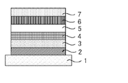
- FIG. 1 A specific example of the structure of an organic electroluminescence element is shown in FIG. In FIG. 1, 1 is a substrate, 2 is an anode, 3 is a hole injection layer, 4 is a hole transport layer, 5 is a light emitting layer, 6 is an electron transport layer, and 7 is a cathode. Below, each member and each layer of an organic electroluminescent element are demonstrated. In addition, description of a board
- the organic electroluminescence device of the present invention is preferably supported on a substrate.
- the substrate is not particularly limited and may be any substrate conventionally used for organic electroluminescence elements.
- a substrate made of glass, transparent plastic, quartz, silicon, or the like can be used.
- an electrode material made of a metal, an alloy, an electrically conductive compound, or a mixture thereof having a high work function (4 eV or more) is preferably used.
- electrode materials include metals such as Au, and conductive transparent materials such as CuI, indium tin oxide (ITO), SnO 2 , and ZnO.
- conductive transparent materials such as CuI, indium tin oxide (ITO), SnO 2 , and ZnO.
- an amorphous material such as IDIXO (In 2 O 3 —ZnO) that can form a transparent conductive film may be used.
- a thin film may be formed by vapor deposition or sputtering of these electrode materials, and a pattern of a desired shape may be formed by photolithography, or when pattern accuracy is not so high (about 100 ⁇ m or more) ), A pattern may be formed through a mask having a desired shape at the time of vapor deposition or sputtering of the electrode material.
- wet film-forming methods such as a printing system and a coating system, can also be used.
- the transmittance be greater than 10%, and the sheet resistance as the anode is preferably several hundred ⁇ / ⁇ or less.
- the film thickness depends on the material, it is usually selected in the range of 10 to 1000 nm, preferably 10 to 200 nm.
- cathode a material having a low work function (4 eV or less) metal (referred to as an electron injecting metal), an alloy, an electrically conductive compound, and a mixture thereof as an electrode material is used.
- electrode materials include sodium, sodium-potassium alloy, magnesium, lithium, magnesium / copper mixture, magnesium / silver mixture, magnesium / aluminum mixture, magnesium / indium mixture, aluminum / aluminum oxide (Al 2 O 3 ) Mixtures, indium, lithium / aluminum mixtures, rare earth metals and the like.
- a mixture of an electron injecting metal and a second metal which is a stable metal having a larger work function value than this for example, a magnesium / silver mixture, Magnesium / aluminum mixtures, magnesium / indium mixtures, aluminum / aluminum oxide (Al 2 O 3 ) mixtures, lithium / aluminum mixtures, aluminum and the like are preferred.
- the cathode can be produced by forming a thin film of these electrode materials by a method such as vapor deposition or sputtering.
- the sheet resistance as the cathode is preferably several hundred ⁇ / ⁇ or less, and the film thickness is usually selected in the range of 10 nm to 5 ⁇ m, preferably 50 to 200 nm.
- the emission luminance is advantageously improved.
- a transparent or semi-transparent cathode can be produced. By applying this, an element in which both the anode and the cathode are transparent is used. Can be produced.
- the light emitting layer is a layer that emits light after excitons are generated by recombination of holes and electrons injected from each of the anode and the cathode, and the light emitting material may be used alone for the light emitting layer.
- the luminescent material is composed of the compound defined in the present invention (the luminescent material of the present invention), and may be composed of one kind of the compound defined in the present invention, or defined by the present invention. It may contain two or more types of compounds.
- the organic electroluminescence device and the organic photoluminescence device of the present invention In order for the organic electroluminescence device and the organic photoluminescence device of the present invention to exhibit high luminous efficiency, it is important to confine singlet excitons and triplet excitons generated in the light emitting material in the light emitting material. Therefore, it is preferable to use a host material in addition to the light emitting material in the light emitting layer.
- a host material an organic compound having at least one of excited singlet energy and excited triplet energy higher than that of the light emitting material of the present invention can be used.
- singlet excitons and triplet excitons generated in the light emitting material of the present invention can be confined in the molecules of the light emitting material of the present invention, and the light emission efficiency can be sufficiently extracted.
- light emission is generated from the light emitting material of the present invention contained in the light emitting layer.
- This light emission may be only normal fluorescent light emission that is not delayed (simply referred to as “fluorescent light emission”), or may include both fluorescent light emission and delayed fluorescent light emission.
- light emission from the host material may be partly or partly emitted.
- the amount of the compound of the present invention which is a light emitting material, is preferably 0.1% by weight or more, more preferably 1% by weight or more, and 50% or more. It is preferably no greater than wt%, more preferably no greater than 20 wt%, and even more preferably no greater than 10 wt%.
- the host material in the light-emitting layer is preferably an organic compound that has a hole transporting ability and an electron transporting ability, prevents the emission of longer wavelengths, and has a high glass transition temperature.
- the injection layer is a layer provided between the electrode and the organic layer for lowering the driving voltage and improving the luminance of light emission.
- the injection layer can be provided as necessary.
- the blocking layer is a layer that can prevent diffusion of charges (electrons or holes) and / or excitons existing in the light emitting layer to the outside of the light emitting layer.
- the electron blocking layer can be disposed between the light emitting layer and the hole transport layer and blocks electrons from passing through the light emitting layer toward the hole transport layer.
- a hole blocking layer can be disposed between the light emitting layer and the electron transporting layer to prevent holes from passing through the light emitting layer toward the electron transporting layer.
- the blocking layer can also be used to block excitons from diffusing outside the light emitting layer. That is, each of the electron blocking layer and the hole blocking layer can also function as an exciton blocking layer.
- the term “electron blocking layer” or “exciton blocking layer” as used herein is used in the sense of including a layer having the functions of an electron blocking layer and an exciton blocking layer in one layer.
- the hole blocking layer has a function of an electron transport layer in a broad sense.
- the hole blocking layer has a role of blocking holes from reaching the electron transport layer while transporting electrons, thereby improving the recombination probability of electrons and holes in the light emitting layer.
- the material for the hole blocking layer the material for the electron transport layer described later can be used as necessary.
- the electron blocking layer has a function of transporting holes in a broad sense.
- the electron blocking layer has a role to block electrons from reaching the hole transport layer while transporting holes, thereby improving the probability of recombination of electrons and holes in the light emitting layer. .
- the exciton blocking layer is a layer for preventing excitons generated by recombination of holes and electrons in the light emitting layer from diffusing into the charge transport layer. It becomes possible to efficiently confine in the light emitting layer, and the light emission efficiency of the device can be improved.
- the exciton blocking layer can be inserted on either the anode side or the cathode side adjacent to the light emitting layer, or both can be inserted simultaneously.
- the layer when the exciton blocking layer is provided on the anode side, the layer can be inserted adjacent to the light emitting layer between the hole transport layer and the light emitting layer, and when inserted on the cathode side, the light emitting layer and the cathode Between the luminescent layer and the light-emitting layer.
- a hole injection layer, an electron blocking layer, or the like can be provided between the anode and the exciton blocking layer adjacent to the anode side of the light emitting layer, and the excitation adjacent to the cathode and the cathode side of the light emitting layer can be provided.
- an electron injection layer, an electron transport layer, a hole blocking layer, and the like can be provided.
- the blocking layer is disposed, at least one of the excited singlet energy and the excited triplet energy of the material used as the blocking layer is preferably higher than the excited singlet energy and the excited triplet energy of the light emitting material.
- the hole transport layer is made of a hole transport material having a function of transporting holes, and the hole transport layer can be provided as a single layer or a plurality of layers.
- the hole transport material has any one of hole injection or transport and electron barrier properties, and may be either organic or inorganic.
- hole transport materials that can be used include, for example, triazole derivatives, oxadiazole derivatives, imidazole derivatives, carbazole derivatives, indolocarbazole derivatives, polyarylalkane derivatives, pyrazoline derivatives and pyrazolone derivatives, phenylenediamine derivatives, arylamine derivatives, Examples include amino-substituted chalcone derivatives, oxazole derivatives, styrylanthracene derivatives, fluorenone derivatives, hydrazone derivatives, stilbene derivatives, silazane derivatives, aniline copolymers, and conductive polymer oligomers, particularly thiophene oligomers.
- An aromatic tertiary amine compound and an styrylamine compound are preferably used, and an aromatic tertiary amine compound is more preferably used.
- the electron transport layer is made of a material having a function of transporting electrons, and the electron transport layer can be provided as a single layer or a plurality of layers.
- the electron transport material (which may also serve as a hole blocking material) may have a function of transmitting electrons injected from the cathode to the light emitting layer.
- Examples of the electron transport layer that can be used include nitro-substituted fluorene derivatives, diphenylquinone derivatives, thiopyran dioxide oxide derivatives, carbodiimides, fluorenylidenemethane derivatives, anthraquinodimethane and anthrone derivatives, oxadiazole derivatives, and the like.
- a thiadiazole derivative in which the oxygen atom of the oxadiazole ring is substituted with a sulfur atom, and a quinoxaline derivative having a quinoxaline ring known as an electron withdrawing group can also be used as an electron transport material.
- a polymer material in which these materials are introduced into a polymer chain or these materials are used as a polymer main chain can also be used.
- the compound represented by the general formula (1) may be used not only for the light emitting layer but also for layers other than the light emitting layer.
- the compound represented by General formula (1) used for a light emitting layer and the compound represented by General formula (1) used for layers other than a light emitting layer may be same or different.
- the compound represented by the general formula (1) may be used for the injection layer, blocking layer, hole blocking layer, electron blocking layer, exciton blocking layer, hole transporting layer, electron transporting layer, and the like. .
- the method for forming these layers is not particularly limited, and the layer may be formed by either a dry process or a wet process.
- the preferable material which can be used for an organic electroluminescent element is illustrated concretely.
- the material that can be used in the present invention is not limited to the following exemplary compounds.
- R, R ′, and R 1 to R 10 each independently represent a hydrogen atom or a substituent.
- X represents a carbon atom or a hetero atom forming a ring skeleton
- n represents an integer of 3 to 5
- Y represents a substituent
- m represents an integer of 0 or more.
- the organic electroluminescence device produced by the above-described method emits light by applying an electric field between the anode and the cathode of the obtained device. At this time, if the light is emitted by excited singlet energy, light having a wavelength corresponding to the energy level is confirmed as fluorescence emission and delayed fluorescence emission. In addition, in the case of light emission by excited triplet energy, a wavelength corresponding to the energy level is confirmed as phosphorescence. Since normal fluorescence has a shorter fluorescence lifetime than delayed fluorescence, the emission lifetime can be distinguished from fluorescence and delayed fluorescence.
- the excited triplet energy is unstable and is converted into heat and the like, and the lifetime is short and it is immediately deactivated.
- the excited triplet energy of a normal organic compound it can be measured by observing light emission under extremely low temperature conditions.
- the organic electroluminescence element of the present invention can be applied to any of a single element, an element having a structure arranged in an array, and a structure in which an anode and a cathode are arranged in an XY matrix. According to the present invention, an organic light emitting device with greatly improved luminous efficiency can be obtained by incorporating a compound having a specific structure in the light emitting layer.
- the organic light emitting device such as the organic electroluminescence device of the present invention can be further applied to various uses. For example, it is possible to produce an organic electroluminescence display device using the organic electroluminescence element of the present invention. For details, see “Organic EL Display” (Ohm Co., Ltd.) ) Can be referred to.
- the organic electroluminescence device of the present invention can be applied to organic electroluminescence illumination and backlights that are in great demand.
- source meter manufactured by Keithley: 2400 series
- semiconductor parameter analyzer manufactured by Agilent Technologies: E5273A
- optical power meter measuring device manufactured by Newport: 1930C
- optical spectrometer Ocean Optics, USB2000
- spectroradiometer Topcon, SR-3
- streak camera Haamamatsu Photonics C4334
- the HOMO and LUMO energy levels of the compounds used in the examples and comparative examples were determined by the following methods.
- the energy level of HOMO is obtained by measuring the oxidation potential (half-wave potential of the first oxidation wave) of each compound in dichloromethane and using the following formula provided in Org. Electronics, 2005, 6, 11-20. It was.
- HOMO (ev) ⁇ 1.4E 1/2 (vs. Fc / Fc + ) ⁇ 4.6
- E 1/2 (vs. Fc / Fc + ) is a half-wave potential of the first oxidation wave with reference to the ferrocene electrode.
- the LUMO energy level is determined by determining the energy gap E gap between the HOMO energy level and the LUMO energy level from the absorption spectrum, and calculating the difference between the measured value of the HOMO energy level and the energy gap E gap. Asked.
- the energy gap E gap was determined from the wavelength value at the intersection of the rising tangent on the short wavelength side of the absorption spectrum and the horizontal axis.
- the reaction solution was cooled to room temperature, and separated into two layers, an aqueous layer and an organic layer. Among these, the aqueous layer was collected and extracted three times with 30 mL of ethyl acetate. The obtained organic layer was washed twice with 30 mL of saturated brine, dried by adding sodium sulfate, and then filtered. The solvent was removed from the filtrate, and the obtained residue was purified by silica gel column chromatography using a mixed solvent of dichloromethane: hexane (1: 3) as an eluent. When the obtained fraction was concentrated, a white solid of the target compound 1 was obtained in a yield of 1.1 g and a yield of 77%.
- the reaction solution was cooled to room temperature and 50 mL of water was added to separate the aqueous layer and the organic layer into two layers. Among these, the aqueous layer was collected and extracted three times with 30 mL of ethyl acetate. The obtained organic layer was washed twice with 30 mL of saturated brine, dried by adding sodium sulfate, and then filtered. The solvent was removed from the obtained filtrate, and the remaining residue was purified by silica gel column chromatography using hexane as an eluent. By concentrating the obtained fraction, a white solid of intermediate a was obtained in a yield of 5.25 g and a yield of 52%.
- 5-phenyl-5,10-dihydrophenazine (20 mmol, 30 mL as a toluene solution), 4-iodo-bromobenzene (5.66 g, 20 mmol), copper iodide (110 mg, 0.6 mmol), sodium tert-butoxide (2 .95 g, 30 mmol), 0.20 mL of 1,2-diaminocyclohexane and 50 mL of 1,4-dioxane were placed in a container, the inside of the container was replaced with nitrogen, and the mixture in the container was stirred at 100 ° C. for 24 hours.
- Compound 9 was synthesized according to the following procedure. 9,9-dimethyl-10- (4- (4,4,5,5-tetramethyl-1,3,2-dioxaborolan-2-yl) phenyl) -9,10-dihydroacridine (2.05 g, 5 mmol ), Di-2,7-bromo-9,9-dimethylfluorene (704 mg, 2 mmol), tetrakis (triphenylphosphine) palladium (0) (232 mg, 0.2 mmol), potassium carbonate (6.91 g), 150 mL of tetrahydrofuran And 70 mL of water was put into the container, and the inside of the container was degassed under reduced pressure, and then replaced with nitrogen.
- the container was placed in an oil bath and the mixture in the container was heated at 80 ° C. for 24 hours. After heating, the reaction solution was cooled to room temperature, and the deposited precipitate was collected by filtration. The obtained crude product was purified by a sublimation method to obtain the target compound 9 as a white solid in a yield of 852 mg and a yield of 56%.
- the starting material 4- (9,9-dimethyl-9,10-dihydroacridine) bromobenzene was synthesized by the method described in J. Am. Chem. Soc. 2014, 136, 18070-18081
- 4- (3,6-di-tert-butylcarbazole) bromobenzene was synthesized by the method described in W. Chem. Lett. 2008, 37, 986
- 5-phenyl-5,10-dihydrophenazine was Synthesized by the method described in J. Org. Chem. 70, 10073-10081 (2005).
- Examples 1 to 11 Preparation and Evaluation of Solutions Using Compounds 1 to 11 Toluene solutions of compounds 1 to 11 (concentration 10 ⁇ 5 mol / L) were prepared, and nitrogen gas replacement was performed. With respect to the prepared solutions of each compound, an absorption spectrum and an emission spectrum by 340 nm excitation light were obtained. Table 1 shows the maximum absorption wavelength of the absorption spectrum and the minimum emission wavelength of the emission spectrum of each solution. Table 1 also shows the HOMO level and the LUMO level.
- Example 12 Production and evaluation of solid organic thin film using compound 2 A thin film of compound 2 having a thickness of 250 nm was formed on a quartz substrate by a vacuum deposition method under a vacuum degree of 2 ⁇ 10 -4 Pa. Thus, a solid organic thin film was obtained. Table 3 shows the maximum emission wavelength and photoluminescence quantum efficiency of the prepared compound 2 thin film.
- Example 13 Production and evaluation of solid organic thin film using compound 11 A thin film of compound 11 having a thickness of 200 nm was formed on a quartz substrate by a vacuum vapor deposition method under the condition of a vacuum degree of 2 ⁇ 10 -4 Pa. Thus, a solid organic thin film was obtained. Separately, the compound 11 and PPT or DPEPO are co-deposited from different vapor deposition sources on a quartz substrate by a vacuum vapor deposition method under a vacuum degree of 2 ⁇ 10 ⁇ 4 Pa, and the concentration of the compound 11 is 8 wt%. A thin film having a thickness of 200 nm was formed into a solid organic thin film. Table 2 shows the results of measuring the maximum emission wavelength and the photoluminescence quantum yield (PL quantum yield) of each thin film produced.
- PL quantum yield photoluminescence quantum yield
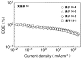
- Example 14 Production and evaluation of organic electroluminescence device using compound 2 Each thin film was vacuum-deposited on a glass substrate on which an anode made of indium tin oxide (ITO) having a thickness of 100 nm was formed. And a degree of vacuum of 2 ⁇ 10 ⁇ 4 Pa. First, ⁇ -NPD was formed to a thickness of 40 nm on ITO, and mCP was formed to a thickness of 10 nm thereon. Next, Compound 2 was deposited to a thickness of 25 nm to form a light emitting layer, and TPBi was formed to a thickness of 40 nm thereon.
- ITO indium tin oxide
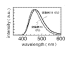
- FIG. 2 shows the emission spectrum (PL) of the solid organic thin film produced in Example 12.
- Example 15 Preparation and evaluation of organic electroluminescence device using compound 11 [1] Each thin film was laminated at a vacuum degree of 2 ⁇ 10 ⁇ 4 Pa by a vacuum deposition method on a glass substrate on which an anode made of indium tin oxide (ITO) having a thickness of 100 nm was formed. First, TAPC was formed to a thickness of 40 nm on ITO. Next, Compound 11 was deposited to a thickness of 20 nm to form a light emitting layer. Subsequently, DPEPO was formed to a thickness of 10 nm, and TPBi was formed thereon to a thickness of 40 nm.
- ITO indium tin oxide
- LiF lithium fluoride
- Al aluminum
- Example 16 Preparation and evaluation of organic electroluminescence device using compound 11 [2] Each thin film was laminated at a vacuum degree of 2 ⁇ 10 ⁇ 4 Pa by a vacuum deposition method on a glass substrate on which an anode made of indium tin oxide (ITO) having a thickness of 100 nm was formed. First, TAPC was formed to a thickness of 40 nm on ITO. Next, Compound 11 and PPT were co-evaporated from different vapor deposition sources to form a 20 nm thick layer to be a light emitting layer. At this time, the concentration of Compound 11 was 8% by weight.
- ITO indium tin oxide
- PPT was formed to a thickness of 10 nm, and TPBi was formed thereon to a thickness of 40 nm. Further, lithium fluoride (LiF) was formed to a thickness of 1 nm, and then aluminum (Al) was evaporated to a thickness of 100 nm to form a cathode, whereby an organic electroluminescent element was obtained.
- Table 3 shows the element characteristics of the manufactured organic electroluminescence element.
- Example 17 Preparation and evaluation of organic electroluminescence device using compound 11 [3] Each thin film was laminated at a vacuum degree of 2 ⁇ 10 ⁇ 4 Pa by a vacuum deposition method on a glass substrate on which an anode made of indium tin oxide (ITO) having a thickness of 100 nm was formed. First, TAPC was formed to a thickness of 40 nm on ITO. Next, Compound 11 and DPEPO were co-deposited from different vapor deposition sources to form a 20 nm thick layer as a light emitting layer. At this time, the concentration of Compound 11 was 8% by weight.
- ITO indium tin oxide
- DPEPO was formed to a thickness of 10 nm, and TPBi was formed thereon to a thickness of 40 nm. Further, lithium fluoride (LiF) was formed to a thickness of 1 nm, and then aluminum (Al) was evaporated to a thickness of 100 nm to form a cathode, whereby an organic electroluminescent element was obtained.
- Table 3 shows the element characteristics of the manufactured organic electroluminescence element.
- Example 18 Production and evaluation of organic electroluminescence device using compound 11 [4] Each thin film was laminated at a vacuum degree of 2 ⁇ 10 ⁇ 4 Pa by a vacuum deposition method on a glass substrate on which an anode made of indium tin oxide (ITO) having a thickness of 100 nm was formed. First, TAPC was formed to a thickness of 40 nm on ITO. Next, Compound 11 and DPEPO were co-deposited from different vapor deposition sources to form a 20 nm thick layer as a light emitting layer. At this time, the concentration of Compound 11 was 8% by weight. Subsequently, a layer gradually changing from DPEPO to TPBi was formed to a thickness of 10 nm.
- ITO indium tin oxide
- FIG. 4 shows the emission spectrum of the produced organic electroluminescence device
- FIG. 5 shows the voltage-current density-luminance characteristics
- FIG. 6 shows the current density-external quantum efficiency characteristics.
- Table 3 shows element characteristics of the organic electroluminescence element.
- Each of the manufactured organic electroluminescence elements had good element characteristics. From this, it was confirmed that a compound having a donor group but not having an acceptor group has a sufficient function as a light-emitting material of an organic electroluminescence element.
- the compound of the present invention is useful as a luminescent material. For this reason, the compound of this invention is effectively used as a luminescent material for organic light emitting elements, such as an organic electroluminescent element. Since the compounds of the present invention include those that emit delayed fluorescence, it is also possible to provide an organic light-emitting device with high luminous efficiency. For this reason, this invention has high industrial applicability.
Landscapes
- Chemical & Material Sciences (AREA)
- Organic Chemistry (AREA)
- Engineering & Computer Science (AREA)
- Materials Engineering (AREA)
- Physics & Mathematics (AREA)
- Spectroscopy & Molecular Physics (AREA)
- Optics & Photonics (AREA)
- Electroluminescent Light Sources (AREA)
- Heterocyclic Carbon Compounds Containing A Hetero Ring Having Nitrogen And Oxygen As The Only Ring Hetero Atoms (AREA)
- Plural Heterocyclic Compounds (AREA)
- Indole Compounds (AREA)
- Other In-Based Heterocyclic Compounds (AREA)
Abstract
L'invention concerne un composé qui est constitué d'au moins deux groupes donneurs de structures différentes, et d'un groupe de liaison liant ces groupes donneurs. Ce composé dans lequel ledit groupe de liaison consiste en un groupe aromatique configuré par au moins un cycle benzène pouvant être substitué par un groupe alkyl ou un groupe halogène, possède des caractéristiques luminescentes satisfaisantes.
Priority Applications (1)
| Application Number | Priority Date | Filing Date | Title |
|---|---|---|---|
| US16/083,633 US20200343453A1 (en) | 2016-03-11 | 2017-03-10 | Light-emitting material, organic light-emitting element, and compound |
Applications Claiming Priority (2)
| Application Number | Priority Date | Filing Date | Title |
|---|---|---|---|
| JP2016-048057 | 2016-03-11 | ||
| JP2016048057A JP2017163075A (ja) | 2016-03-11 | 2016-03-11 | 発光材料、有機発光素子および化合物 |
Publications (1)
| Publication Number | Publication Date |
|---|---|
| WO2017155102A1 true WO2017155102A1 (fr) | 2017-09-14 |
Family
ID=59790550
Family Applications (1)
| Application Number | Title | Priority Date | Filing Date |
|---|---|---|---|
| PCT/JP2017/009762 Ceased WO2017155102A1 (fr) | 2016-03-11 | 2017-03-10 | Matériau luminescent, élément luminescent organique, et composé |
Country Status (3)
| Country | Link |
|---|---|
| US (1) | US20200343453A1 (fr) |
| JP (1) | JP2017163075A (fr) |
| WO (1) | WO2017155102A1 (fr) |
Cited By (2)
| Publication number | Priority date | Publication date | Assignee | Title |
|---|---|---|---|---|
| WO2018155642A1 (fr) * | 2017-02-24 | 2018-08-30 | 国立大学法人九州大学 | Composé, matériau électroluminescent et élément électroluminescent |
| US20200295269A1 (en) * | 2019-03-11 | 2020-09-17 | Samsung Display Co., Ltd. | Heterocyclic compound and organic light-emitting device including the same |
Families Citing this family (1)
| Publication number | Priority date | Publication date | Assignee | Title |
|---|---|---|---|---|
| KR20220006001A (ko) | 2020-07-07 | 2022-01-14 | 호도가야 가가쿠 고교 가부시키가이샤 | 유기 패터닝층, 및 그것을 사용한 금속 패터닝 방법 |
Citations (5)
| Publication number | Priority date | Publication date | Assignee | Title |
|---|---|---|---|---|
| JPH11224779A (ja) * | 1998-02-04 | 1999-08-17 | Mitsui Chem Inc | 有機電界発光素子 |
| JP2004091350A (ja) * | 2002-08-30 | 2004-03-25 | Canon Inc | モノアミノフルオレン化合物およびそれを使用した有機発光素子 |
| KR20100132109A (ko) * | 2009-06-09 | 2010-12-17 | 주식회사 이엘엠 | 유기 전기 발광 조성물 및 이를 포함하는 유기 전기 발광 소자 |
| JP2013521238A (ja) * | 2010-03-02 | 2013-06-10 | メルク パテント ゲーエムベーハー | 電子デバイス用化合物 |
| KR20140020208A (ko) * | 2012-08-07 | 2014-02-18 | 주식회사 동진쎄미켐 | 아크리딘 유도체를 포함하는 유기발광 화합물 및 이를 포함하는 유기발광소자 |
-
2016
- 2016-03-11 JP JP2016048057A patent/JP2017163075A/ja active Pending
-
2017
- 2017-03-10 US US16/083,633 patent/US20200343453A1/en not_active Abandoned
- 2017-03-10 WO PCT/JP2017/009762 patent/WO2017155102A1/fr not_active Ceased
Patent Citations (5)
| Publication number | Priority date | Publication date | Assignee | Title |
|---|---|---|---|---|
| JPH11224779A (ja) * | 1998-02-04 | 1999-08-17 | Mitsui Chem Inc | 有機電界発光素子 |
| JP2004091350A (ja) * | 2002-08-30 | 2004-03-25 | Canon Inc | モノアミノフルオレン化合物およびそれを使用した有機発光素子 |
| KR20100132109A (ko) * | 2009-06-09 | 2010-12-17 | 주식회사 이엘엠 | 유기 전기 발광 조성물 및 이를 포함하는 유기 전기 발광 소자 |
| JP2013521238A (ja) * | 2010-03-02 | 2013-06-10 | メルク パテント ゲーエムベーハー | 電子デバイス用化合物 |
| KR20140020208A (ko) * | 2012-08-07 | 2014-02-18 | 주식회사 동진쎄미켐 | 아크리딘 유도체를 포함하는 유기발광 화합물 및 이를 포함하는 유기발광소자 |
Cited By (4)
| Publication number | Priority date | Publication date | Assignee | Title |
|---|---|---|---|---|
| WO2018155642A1 (fr) * | 2017-02-24 | 2018-08-30 | 国立大学法人九州大学 | Composé, matériau électroluminescent et élément électroluminescent |
| US12120952B2 (en) | 2017-02-24 | 2024-10-15 | Kyulux, Inc. | Compound, light-emitting material and light-emitting element |
| US20200295269A1 (en) * | 2019-03-11 | 2020-09-17 | Samsung Display Co., Ltd. | Heterocyclic compound and organic light-emitting device including the same |
| US12004422B2 (en) * | 2019-03-11 | 2024-06-04 | Samsung Display Co., Ltd. | Heterocyclic compound and organic light-emitting device including the same |
Also Published As
| Publication number | Publication date |
|---|---|
| US20200343453A1 (en) | 2020-10-29 |
| JP2017163075A (ja) | 2017-09-14 |
Similar Documents
| Publication | Publication Date | Title |
|---|---|---|
| JP7758385B2 (ja) | 化合物、発光材料および発光素子 | |
| JP6318155B2 (ja) | 化合物、発光材料および有機発光素子 | |
| JP6263524B2 (ja) | 化合物、発光材料および有機発光素子 | |
| JP6293417B2 (ja) | 化合物、発光材料および有機発光素子 | |
| JP5594750B2 (ja) | 化合物、発光材料および有機発光素子 | |
| JP6383538B2 (ja) | 発光材料、有機発光素子および化合物 | |
| JP6466913B2 (ja) | 発光材料、有機発光素子および化合物 | |
| JP6225111B2 (ja) | 発光材料、化合物、およびそれらを用いた有機発光素子 | |
| JP6367189B2 (ja) | 発光材料、有機発光素子および化合物 | |
| WO2015080183A1 (fr) | Substance électroluminescente, élément électroluminescent organique, et composé | |
| JP2018100411A (ja) | 発光材料、化合物および有機発光素子 | |
| JP2017119663A (ja) | 化合物、発光材料および有機発光素子 | |
| JPWO2013161437A1 (ja) | 発光材料および有機発光素子 | |
| WO2015133501A1 (fr) | Matériau électroluminescent, élément organique électroluminescent et composé | |
| WO2015002213A1 (fr) | Matériau électroluminescent, substance fluorescente de longue durée, élément électroluminescent organique et composé | |
| JP2017222623A (ja) | 化合物および有機発光素子 | |
| JP2015134874A (ja) | 発光材料、有機発光素子および化合物 | |
| WO2014189122A1 (fr) | Composé, matériau électroluminescent et élément électroluminescent organique | |
| JP6249150B2 (ja) | 発光材料およびそれを用いた有機発光素子 | |
| JP6647514B2 (ja) | 有機発光素子ならびにそれに用いる発光材料および化合物 | |
| WO2017155102A1 (fr) | Matériau luminescent, élément luminescent organique, et composé | |
| WO2017115834A1 (fr) | Composé, matériau électroluminescent et élément électroluminescent organique | |
| JP2018111751A (ja) | 発光材料、化合物および有機発光素子 | |
| JP2016084283A (ja) | 化合物、発光材料および有機発光素子 |
Legal Events
| Date | Code | Title | Description |
|---|---|---|---|
| NENP | Non-entry into the national phase |
Ref country code: DE |
|
| 121 | Ep: the epo has been informed by wipo that ep was designated in this application |
Ref document number: 17763434 Country of ref document: EP Kind code of ref document: A1 |
|
| 122 | Ep: pct application non-entry in european phase |
Ref document number: 17763434 Country of ref document: EP Kind code of ref document: A1 |