WO2017157015A1 - 阵列摄像模组及其模塑感光组件和制造方法以及电子设备 - Google Patents
阵列摄像模组及其模塑感光组件和制造方法以及电子设备 Download PDFInfo
- Publication number
- WO2017157015A1 WO2017157015A1 PCT/CN2016/103736 CN2016103736W WO2017157015A1 WO 2017157015 A1 WO2017157015 A1 WO 2017157015A1 CN 2016103736 W CN2016103736 W CN 2016103736W WO 2017157015 A1 WO2017157015 A1 WO 2017157015A1
- Authority
- WO
- WIPO (PCT)
- Prior art keywords
- photosensitive
- chip
- photosensitive member
- camera module
- molded
- Prior art date
- Legal status (The legal status is an assumption and is not a legal conclusion. Google has not performed a legal analysis and makes no representation as to the accuracy of the status listed.)
- Ceased
Links
Images










Classifications
-
- G—PHYSICS
- G02—OPTICS
- G02B—OPTICAL ELEMENTS, SYSTEMS OR APPARATUS
- G02B7/00—Mountings, adjusting means, or light-tight connections, for optical elements
- G02B7/02—Mountings, adjusting means, or light-tight connections, for optical elements for lenses
- G02B7/021—Mountings, adjusting means, or light-tight connections, for optical elements for lenses for more than one lens
-
- H—ELECTRICITY
- H04—ELECTRIC COMMUNICATION TECHNIQUE
- H04N—PICTORIAL COMMUNICATION, e.g. TELEVISION
- H04N23/00—Cameras or camera modules comprising electronic image sensors; Control thereof
- H04N23/50—Constructional details
-
- B—PERFORMING OPERATIONS; TRANSPORTING
- B29—WORKING OF PLASTICS; WORKING OF SUBSTANCES IN A PLASTIC STATE IN GENERAL
- B29C—SHAPING OR JOINING OF PLASTICS; SHAPING OF MATERIAL IN A PLASTIC STATE, NOT OTHERWISE PROVIDED FOR; AFTER-TREATMENT OF THE SHAPED PRODUCTS, e.g. REPAIRING
- B29C45/00—Injection moulding, i.e. forcing the required volume of moulding material through a nozzle into a closed mould; Apparatus therefor
- B29C45/14—Injection moulding, i.e. forcing the required volume of moulding material through a nozzle into a closed mould; Apparatus therefor incorporating preformed parts or layers, e.g. injection moulding around inserts or for coating articles
- B29C45/14639—Injection moulding, i.e. forcing the required volume of moulding material through a nozzle into a closed mould; Apparatus therefor incorporating preformed parts or layers, e.g. injection moulding around inserts or for coating articles for obtaining an insulating effect, e.g. for electrical components
-
- G—PHYSICS
- G02—OPTICS
- G02B—OPTICAL ELEMENTS, SYSTEMS OR APPARATUS
- G02B13/00—Optical objectives specially designed for the purposes specified below
- G02B13/001—Miniaturised objectives for electronic devices, e.g. portable telephones, webcams, PDAs, small digital cameras
-
- G—PHYSICS
- G02—OPTICS
- G02B—OPTICAL ELEMENTS, SYSTEMS OR APPARATUS
- G02B13/00—Optical objectives specially designed for the purposes specified below
- G02B13/001—Miniaturised objectives for electronic devices, e.g. portable telephones, webcams, PDAs, small digital cameras
- G02B13/0015—Miniaturised objectives for electronic devices, e.g. portable telephones, webcams, PDAs, small digital cameras characterised by the lens design
- G02B13/002—Miniaturised objectives for electronic devices, e.g. portable telephones, webcams, PDAs, small digital cameras characterised by the lens design having at least one aspherical surface
- G02B13/004—Miniaturised objectives for electronic devices, e.g. portable telephones, webcams, PDAs, small digital cameras characterised by the lens design having at least one aspherical surface having four lenses
-
- G—PHYSICS
- G02—OPTICS
- G02B—OPTICAL ELEMENTS, SYSTEMS OR APPARATUS
- G02B3/00—Simple or compound lenses
- G02B3/0006—Arrays
- G02B3/0075—Arrays characterized by non-optical structures, e.g. having integrated holding or alignment means
-
- G—PHYSICS
- G02—OPTICS
- G02B—OPTICAL ELEMENTS, SYSTEMS OR APPARATUS
- G02B5/00—Optical elements other than lenses
- G02B5/20—Filters
- G02B5/201—Filters in the form of arrays
-
- G—PHYSICS
- G02—OPTICS
- G02B—OPTICAL ELEMENTS, SYSTEMS OR APPARATUS
- G02B7/00—Mountings, adjusting means, or light-tight connections, for optical elements
- G02B7/006—Filter holders
-
- H—ELECTRICITY
- H04—ELECTRIC COMMUNICATION TECHNIQUE
- H04N—PICTORIAL COMMUNICATION, e.g. TELEVISION
- H04N23/00—Cameras or camera modules comprising electronic image sensors; Control thereof
- H04N23/45—Cameras or camera modules comprising electronic image sensors; Control thereof for generating image signals from two or more image sensors being of different type or operating in different modes, e.g. with a CMOS sensor for moving images in combination with a charge-coupled device [CCD] for still images
-
- H—ELECTRICITY
- H04—ELECTRIC COMMUNICATION TECHNIQUE
- H04N—PICTORIAL COMMUNICATION, e.g. TELEVISION
- H04N23/00—Cameras or camera modules comprising electronic image sensors; Control thereof
- H04N23/50—Constructional details
- H04N23/51—Housings
-
- H—ELECTRICITY
- H04—ELECTRIC COMMUNICATION TECHNIQUE
- H04N—PICTORIAL COMMUNICATION, e.g. TELEVISION
- H04N23/00—Cameras or camera modules comprising electronic image sensors; Control thereof
- H04N23/50—Constructional details
- H04N23/54—Mounting of pick-up tubes, electronic image sensors, deviation or focusing coils
-
- H—ELECTRICITY
- H04—ELECTRIC COMMUNICATION TECHNIQUE
- H04N—PICTORIAL COMMUNICATION, e.g. TELEVISION
- H04N23/00—Cameras or camera modules comprising electronic image sensors; Control thereof
- H04N23/50—Constructional details
- H04N23/55—Optical parts specially adapted for electronic image sensors; Mounting thereof
-
- H—ELECTRICITY
- H04—ELECTRIC COMMUNICATION TECHNIQUE
- H04N—PICTORIAL COMMUNICATION, e.g. TELEVISION
- H04N23/00—Cameras or camera modules comprising electronic image sensors; Control thereof
- H04N23/57—Mechanical or electrical details of cameras or camera modules specially adapted for being embedded in other devices
-
- H—ELECTRICITY
- H05—ELECTRIC TECHNIQUES NOT OTHERWISE PROVIDED FOR
- H05K—PRINTED CIRCUITS; CASINGS OR CONSTRUCTIONAL DETAILS OF ELECTRIC APPARATUS; MANUFACTURE OF ASSEMBLAGES OF ELECTRICAL COMPONENTS
- H05K1/00—Printed circuits
- H05K1/02—Details
- H05K1/0201—Thermal arrangements, e.g. for cooling, heating or preventing overheating
- H05K1/0203—Cooling of mounted components
-
- H—ELECTRICITY
- H05—ELECTRIC TECHNIQUES NOT OTHERWISE PROVIDED FOR
- H05K—PRINTED CIRCUITS; CASINGS OR CONSTRUCTIONAL DETAILS OF ELECTRIC APPARATUS; MANUFACTURE OF ASSEMBLAGES OF ELECTRICAL COMPONENTS
- H05K1/00—Printed circuits
- H05K1/02—Details
- H05K1/0274—Optical details, e.g. printed circuits comprising integral optical means
-
- H—ELECTRICITY
- H05—ELECTRIC TECHNIQUES NOT OTHERWISE PROVIDED FOR
- H05K—PRINTED CIRCUITS; CASINGS OR CONSTRUCTIONAL DETAILS OF ELECTRIC APPARATUS; MANUFACTURE OF ASSEMBLAGES OF ELECTRICAL COMPONENTS
- H05K1/00—Printed circuits
- H05K1/18—Printed circuits structurally associated with non-printed electric components
- H05K1/182—Printed circuits structurally associated with non-printed electric components associated with components mounted in printed circuit boards [PCB], e.g. insert-mounted components [IMC]
- H05K1/183—Printed circuits structurally associated with non-printed electric components associated with components mounted in printed circuit boards [PCB], e.g. insert-mounted components [IMC] associated with components mounted in and supported by recessed areas of the PCBs
-
- H—ELECTRICITY
- H05—ELECTRIC TECHNIQUES NOT OTHERWISE PROVIDED FOR
- H05K—PRINTED CIRCUITS; CASINGS OR CONSTRUCTIONAL DETAILS OF ELECTRIC APPARATUS; MANUFACTURE OF ASSEMBLAGES OF ELECTRICAL COMPONENTS
- H05K1/00—Printed circuits
- H05K1/18—Printed circuits structurally associated with non-printed electric components
- H05K1/182—Printed circuits structurally associated with non-printed electric components associated with components mounted in printed circuit boards [PCB], e.g. insert-mounted components [IMC]
- H05K1/185—Printed circuits structurally associated with non-printed electric components associated with components mounted in printed circuit boards [PCB], e.g. insert-mounted components [IMC] associated with components encapsulated in the insulating substrate of the PCBs; associated with components incorporated in internal layers of multilayer circuit boards
-
- H—ELECTRICITY
- H05—ELECTRIC TECHNIQUES NOT OTHERWISE PROVIDED FOR
- H05K—PRINTED CIRCUITS; CASINGS OR CONSTRUCTIONAL DETAILS OF ELECTRIC APPARATUS; MANUFACTURE OF ASSEMBLAGES OF ELECTRICAL COMPONENTS
- H05K1/00—Printed circuits
- H05K1/18—Printed circuits structurally associated with non-printed electric components
- H05K1/189—Printed circuits structurally associated with non-printed electric components characterised by the use of flexible or folded printed circuits
-
- H—ELECTRICITY
- H05—ELECTRIC TECHNIQUES NOT OTHERWISE PROVIDED FOR
- H05K—PRINTED CIRCUITS; CASINGS OR CONSTRUCTIONAL DETAILS OF ELECTRIC APPARATUS; MANUFACTURE OF ASSEMBLAGES OF ELECTRICAL COMPONENTS
- H05K3/00—Apparatus or processes for manufacturing printed circuits
- H05K3/22—Secondary treatment of printed circuits
- H05K3/28—Applying non-metallic protective coatings
- H05K3/284—Applying non-metallic protective coatings for encapsulating mounted components
-
- H—ELECTRICITY
- H10—SEMICONDUCTOR DEVICES; ELECTRIC SOLID-STATE DEVICES NOT OTHERWISE PROVIDED FOR
- H10F—INORGANIC SEMICONDUCTOR DEVICES SENSITIVE TO INFRARED RADIATION, LIGHT, ELECTROMAGNETIC RADIATION OF SHORTER WAVELENGTH OR CORPUSCULAR RADIATION
- H10F39/00—Integrated devices, or assemblies of multiple devices, comprising at least one element covered by group H10F30/00, e.g. radiation detectors comprising photodiode arrays
- H10F39/011—Manufacture or treatment of image sensors covered by group H10F39/12
- H10F39/018—Manufacture or treatment of image sensors covered by group H10F39/12 of hybrid image sensors
-
- H—ELECTRICITY
- H10—SEMICONDUCTOR DEVICES; ELECTRIC SOLID-STATE DEVICES NOT OTHERWISE PROVIDED FOR
- H10F—INORGANIC SEMICONDUCTOR DEVICES SENSITIVE TO INFRARED RADIATION, LIGHT, ELECTROMAGNETIC RADIATION OF SHORTER WAVELENGTH OR CORPUSCULAR RADIATION
- H10F39/00—Integrated devices, or assemblies of multiple devices, comprising at least one element covered by group H10F30/00, e.g. radiation detectors comprising photodiode arrays
- H10F39/011—Manufacture or treatment of image sensors covered by group H10F39/12
- H10F39/024—Manufacture or treatment of image sensors covered by group H10F39/12 of coatings or optical elements
-
- H—ELECTRICITY
- H10—SEMICONDUCTOR DEVICES; ELECTRIC SOLID-STATE DEVICES NOT OTHERWISE PROVIDED FOR
- H10F—INORGANIC SEMICONDUCTOR DEVICES SENSITIVE TO INFRARED RADIATION, LIGHT, ELECTROMAGNETIC RADIATION OF SHORTER WAVELENGTH OR CORPUSCULAR RADIATION
- H10F39/00—Integrated devices, or assemblies of multiple devices, comprising at least one element covered by group H10F30/00, e.g. radiation detectors comprising photodiode arrays
- H10F39/011—Manufacture or treatment of image sensors covered by group H10F39/12
- H10F39/026—Wafer-level processing
-
- H—ELECTRICITY
- H10—SEMICONDUCTOR DEVICES; ELECTRIC SOLID-STATE DEVICES NOT OTHERWISE PROVIDED FOR
- H10F—INORGANIC SEMICONDUCTOR DEVICES SENSITIVE TO INFRARED RADIATION, LIGHT, ELECTROMAGNETIC RADIATION OF SHORTER WAVELENGTH OR CORPUSCULAR RADIATION
- H10F39/00—Integrated devices, or assemblies of multiple devices, comprising at least one element covered by group H10F30/00, e.g. radiation detectors comprising photodiode arrays
- H10F39/80—Constructional details of image sensors
- H10F39/804—Containers or encapsulations
-
- H—ELECTRICITY
- H10—SEMICONDUCTOR DEVICES; ELECTRIC SOLID-STATE DEVICES NOT OTHERWISE PROVIDED FOR
- H10F—INORGANIC SEMICONDUCTOR DEVICES SENSITIVE TO INFRARED RADIATION, LIGHT, ELECTROMAGNETIC RADIATION OF SHORTER WAVELENGTH OR CORPUSCULAR RADIATION
- H10F39/00—Integrated devices, or assemblies of multiple devices, comprising at least one element covered by group H10F30/00, e.g. radiation detectors comprising photodiode arrays
- H10F39/80—Constructional details of image sensors
- H10F39/805—Coatings
- H10F39/8053—Colour filters
-
- H—ELECTRICITY
- H10—SEMICONDUCTOR DEVICES; ELECTRIC SOLID-STATE DEVICES NOT OTHERWISE PROVIDED FOR
- H10F—INORGANIC SEMICONDUCTOR DEVICES SENSITIVE TO INFRARED RADIATION, LIGHT, ELECTROMAGNETIC RADIATION OF SHORTER WAVELENGTH OR CORPUSCULAR RADIATION
- H10F39/00—Integrated devices, or assemblies of multiple devices, comprising at least one element covered by group H10F30/00, e.g. radiation detectors comprising photodiode arrays
- H10F39/80—Constructional details of image sensors
- H10F39/806—Optical elements or arrangements associated with the image sensors
-
- H—ELECTRICITY
- H10—SEMICONDUCTOR DEVICES; ELECTRIC SOLID-STATE DEVICES NOT OTHERWISE PROVIDED FOR
- H10F—INORGANIC SEMICONDUCTOR DEVICES SENSITIVE TO INFRARED RADIATION, LIGHT, ELECTROMAGNETIC RADIATION OF SHORTER WAVELENGTH OR CORPUSCULAR RADIATION
- H10F39/00—Integrated devices, or assemblies of multiple devices, comprising at least one element covered by group H10F30/00, e.g. radiation detectors comprising photodiode arrays
- H10F39/80—Constructional details of image sensors
- H10F39/806—Optical elements or arrangements associated with the image sensors
- H10F39/8063—Microlenses
-
- H—ELECTRICITY
- H10—SEMICONDUCTOR DEVICES; ELECTRIC SOLID-STATE DEVICES NOT OTHERWISE PROVIDED FOR
- H10F—INORGANIC SEMICONDUCTOR DEVICES SENSITIVE TO INFRARED RADIATION, LIGHT, ELECTROMAGNETIC RADIATION OF SHORTER WAVELENGTH OR CORPUSCULAR RADIATION
- H10F39/00—Integrated devices, or assemblies of multiple devices, comprising at least one element covered by group H10F30/00, e.g. radiation detectors comprising photodiode arrays
- H10F39/80—Constructional details of image sensors
- H10F39/809—Constructional details of image sensors of hybrid image sensors
-
- H—ELECTRICITY
- H10—SEMICONDUCTOR DEVICES; ELECTRIC SOLID-STATE DEVICES NOT OTHERWISE PROVIDED FOR
- H10F—INORGANIC SEMICONDUCTOR DEVICES SENSITIVE TO INFRARED RADIATION, LIGHT, ELECTROMAGNETIC RADIATION OF SHORTER WAVELENGTH OR CORPUSCULAR RADIATION
- H10F39/00—Integrated devices, or assemblies of multiple devices, comprising at least one element covered by group H10F30/00, e.g. radiation detectors comprising photodiode arrays
- H10F39/80—Constructional details of image sensors
- H10F39/811—Interconnections
-
- H—ELECTRICITY
- H10—SEMICONDUCTOR DEVICES; ELECTRIC SOLID-STATE DEVICES NOT OTHERWISE PROVIDED FOR
- H10W—GENERIC PACKAGES, INTERCONNECTIONS, CONNECTORS OR OTHER CONSTRUCTIONAL DETAILS OF DEVICES COVERED BY CLASS H10
- H10W90/00—Package configurations
-
- B—PERFORMING OPERATIONS; TRANSPORTING
- B29—WORKING OF PLASTICS; WORKING OF SUBSTANCES IN A PLASTIC STATE IN GENERAL
- B29L—INDEXING SCHEME ASSOCIATED WITH SUBCLASS B29C, RELATING TO PARTICULAR ARTICLES
- B29L2031/00—Other particular articles
- B29L2031/34—Electrical apparatus, e.g. sparking plugs or parts thereof
- B29L2031/3481—Housings or casings incorporating or embedding electric or electronic elements
-
- H—ELECTRICITY
- H05—ELECTRIC TECHNIQUES NOT OTHERWISE PROVIDED FOR
- H05K—PRINTED CIRCUITS; CASINGS OR CONSTRUCTIONAL DETAILS OF ELECTRIC APPARATUS; MANUFACTURE OF ASSEMBLAGES OF ELECTRICAL COMPONENTS
- H05K2201/00—Indexing scheme relating to printed circuits covered by H05K1/00
- H05K2201/01—Dielectrics
- H05K2201/0137—Materials
- H05K2201/0141—Liquid crystal polymer [LCP]
-
- H—ELECTRICITY
- H05—ELECTRIC TECHNIQUES NOT OTHERWISE PROVIDED FOR
- H05K—PRINTED CIRCUITS; CASINGS OR CONSTRUCTIONAL DETAILS OF ELECTRIC APPARATUS; MANUFACTURE OF ASSEMBLAGES OF ELECTRICAL COMPONENTS
- H05K2201/00—Indexing scheme relating to printed circuits covered by H05K1/00
- H05K2201/01—Dielectrics
- H05K2201/0137—Materials
- H05K2201/0158—Polyalkene or polyolefin, e.g. polyethylene [PE], polypropylene [PP]
-
- H—ELECTRICITY
- H05—ELECTRIC TECHNIQUES NOT OTHERWISE PROVIDED FOR
- H05K—PRINTED CIRCUITS; CASINGS OR CONSTRUCTIONAL DETAILS OF ELECTRIC APPARATUS; MANUFACTURE OF ASSEMBLAGES OF ELECTRICAL COMPONENTS
- H05K2201/00—Indexing scheme relating to printed circuits covered by H05K1/00
- H05K2201/01—Dielectrics
- H05K2201/0137—Materials
- H05K2201/0175—Inorganic, non-metallic layer, e.g. resist or dielectric for printed capacitor
-
- H—ELECTRICITY
- H05—ELECTRIC TECHNIQUES NOT OTHERWISE PROVIDED FOR
- H05K—PRINTED CIRCUITS; CASINGS OR CONSTRUCTIONAL DETAILS OF ELECTRIC APPARATUS; MANUFACTURE OF ASSEMBLAGES OF ELECTRICAL COMPONENTS
- H05K2201/00—Indexing scheme relating to printed circuits covered by H05K1/00
- H05K2201/09—Shape and layout
- H05K2201/09009—Substrate related
- H05K2201/09036—Recesses or grooves in insulating substrate
-
- H—ELECTRICITY
- H05—ELECTRIC TECHNIQUES NOT OTHERWISE PROVIDED FOR
- H05K—PRINTED CIRCUITS; CASINGS OR CONSTRUCTIONAL DETAILS OF ELECTRIC APPARATUS; MANUFACTURE OF ASSEMBLAGES OF ELECTRICAL COMPONENTS
- H05K2201/00—Indexing scheme relating to printed circuits covered by H05K1/00
- H05K2201/10—Details of components or other objects attached to or integrated in a printed circuit board
- H05K2201/10007—Types of components
- H05K2201/10121—Optical component, e.g. opto-electronic component
Definitions
- the invention relates to the field of camera modules, and further relates to an array camera module, a molded photosensitive component thereof, a manufacturing method and an electronic device.
- a camera module with more than one lens such as a dual-lens camera module.
- the dual-lens camera module provides a way of simulating the human eye structure, and the dual-lens camera module is in 3D shooting. With scanning, gesture position recognition, color fidelity, fast focus, panoramic deep shooting, background blur shooting and many other aspects have better performance than single-lens camera module, therefore, the camera module with more than one lens is the future The important direction of the development of the camera module industry.
- the dual-lens camera module obtains images from two locations by using two imaging modules with spatial differences, and then separately photographs the two imaging modules according to the image synthesis method.
- the final image of the multi-lens camera module is obtained. It can be understood that, in this process, the consistency of the image effects such as the resolution, shading, and color of each imaging module of the multi-lens camera module, and the deviation values in the horizontal, vertical, and longitudinal directions are measured. An important indicator of the imaging quality of the dual lens camera module.
- FIG. 1A illustrates a prior art dual lens camera module including a circuit board 10P, two mirror mounts 20P, two imaging modules 30P, and a bracket 40P.
- Each of the imaging modules 30P includes a motor lens assembly 31P. .
- Each of the mirror mounts 20P is separately located on the same side of the wiring board 10P, and each of the mirror mounts 20P is connected together by the wiring board 10P, and each of the motor lens assemblies 31P is disposed at each The lens holder 20P is supported by each of the lens holders 20P, and the holder 40P is wrapped around the outside of each of the motor lens assemblies 31P.
- the lens holder 20P may also be a unitary structure, that is, each of the motor lens assemblies 31P may be disposed on the lens holder 20P. different positions.
- each of the lens holders 20P is separately mounted on the circuit board 10P, thereby causing each The size, position, and the like between the mirror holders 20P are difficult to control, so that the consistency of parameters such as size and position between each of the two-lens camera module brackets is poor.
- each of the lens holders 20P is independent, and each of the lens holders 20P is only passed through the circuit board 10P.
- the circuit board 10P since the circuit board 10P usually selects a PCB circuit board, so that the circuit board 10P itself is relatively soft and easily deformed, at this time, the overall rigidity of the dual lens camera module is difficult to ensure, when the double lens Such a structure is liable to cause relative dimensional instability, positional tolerance, and each of the various components of the imaging module 30P, such as the motor lens assembly 31P, during use after the camera module is assembled.
- the optical axis of the imaging module 30P is easily deviated from the preset position and the like. Once any of these conditions occur, the imaging quality of the dual-lens camera module, such as image synthesis, may not be brought to the final imaging effect. Control factors or larger adverse effects.
- the bracket 40P is wrapped around the outer side of each of the motor lens assemblies 31P, and glue is required to be filled between the motor lens assembly 31P and the bracket 40P, causing the size of the dual lens camera module to be further Increase.
- the assembly of the multi-lens camera module is based on a conventional COB (Chip On Board) process
- the circuit board 10P usually has a protruding circuit device 11P, and a photosensitive chip 12P is mounted on the circuit board.
- the photosensitive chip 12P is usually connected to the wiring board 10P through a gold wire 121P, and the gold wire 121P is generally curved and protruded from the wiring board main body, and therefore, the protruding circuit device 11P and The gold wire 121P also brings some disadvantages to the assembly of the camera module.
- the circuit device 11P and the gold wire 21P are directly exposed to the surface of the circuit board 10P, so that in the subsequent assembly process, for example, the process of attaching the lens holder 20P and soldering the motor lens assembly 31P is inevitable.
- the solder resist, dust, and the like at the time of soldering are likely to adhere to the circuit device 11P, and the circuit device 11P and the photo sensor chip 12P are located in a space in which the mutual contact is made, so that dust contaminants are easily affected.
- the photosensitive chip 12P such an effect may cause undesirable phenomena such as black spots on the assembled camera module, and the product yield is lowered.
- the lens holder 20P is located outside the circuit device 11P. Therefore, when the lens holder 20P and the circuit board 10P are mounted, a certain reservation between the lens holder 20P and the circuit device 11P is required.
- the safety distance and the safety distance need to be reserved in the horizontal direction and the upward direction, which increases the thickness of the camera module to a certain extent, making it difficult to reduce the thickness.
- the molding of a multi-camera relative to the molding of a single camera involves coordination problems between a plurality of camera modules, and the optical axes are required to be uniform between the plurality of lenses, and the optical axes of the plurality of lenses based on the conventional COB process are Consistency is hard to secure.
- the overall size of the multi-camera module is relatively large, which is more sensitive to the strength and flatness of the circuit board, so the thickness of the circuit board is large.
- An object of the present invention is to provide an array camera module, a molded photosensitive member thereof, a manufacturing method, and an electronic device, wherein the molded photosensitive member includes a package portion and a photosensitive portion, and the photosensitive portion includes a line a plate and at least two photosensitive elements, the photosensitive element being integrally joined by the joint package and the circuit board.
- An object of the present invention is to provide an array camera module, a molded photosensitive member thereof, a manufacturing method, and an electronic device, wherein the photosensitive member is electrically connected to the circuit board through at least one lead, and the connected package is covered The lead.
- An object of the present invention is to provide an array camera module, a photosensitive member thereof, and a manufacturing method thereof, wherein the photosensitive member has a photosensitive region and a non-sensitive region, and the connected package portion extends to the non-photosensitive region.
- the outer edge of the molded photosensitive member is reduced by expanding the moldable region of the joined package inwardly.
- An object of the present invention is to provide an array camera module, a molded photosensitive member thereof, a manufacturing method, and an electronic device, wherein the molded photosensitive member includes a circuit board and at least one electronic component, and the electronic component protrudes In the circuit board, the electronic component is covered by the connected package so as not to be directly exposed to the outside.
- An object of the present invention is to provide an array camera module, a molded photosensitive member thereof, a manufacturing method thereof, and an electronic device, wherein the joint package portion includes a filter element mounting portion adapted to mount a plurality of filter elements, thereby No additional separate support components are required.
- An object of the present invention is to provide an array camera module, a molded photosensitive member thereof, a manufacturing method thereof, and an electronic device, wherein the circuit board has a plurality of inner grooves, and each of the photosensitive members is disposed in the inner groove In order to reduce the relative height of the photosensitive element and the circuit board, thereby reducing the height requirement of the connected package.
- An object of the present invention is to provide an array camera module, a molded photosensitive member thereof, a manufacturing method thereof, and an electronic device, wherein the circuit board has a plurality of vias and a plurality of outer grooves, and the outer grooves are connected to the a passage, the outer groove being adapted to flip mount the photosensitive element.
- An object of the present invention is to provide an array camera module, a molded photosensitive member thereof, a manufacturing method, and an electronic device, wherein the circuit board portion includes a reinforcing layer laminated on the bottom of the circuit board to enhance the The structural strength and heat dissipation performance of the circuit board.
- An object of the present invention is to provide an array camera module, a molded photosensitive member thereof, a manufacturing method and an electronic device, wherein the circuit board body has at least one reinforcing hole, and the connected package portion extends into the reinforcing hole Thereby enhancing the structural strength of the wire board body.
- An object of the present invention is to provide an array camera module, a molded photosensitive member thereof, a manufacturing method thereof, and an electronic device, wherein the package portion includes a lens mounting portion adapted to mount a plurality of optical lenses, thereby The optical lens provides the mounting position.
- An object of the present invention is to provide an array camera module, a molded photosensitive member thereof, a manufacturing method and an electronic device, wherein the molded photosensitive member provides a supporting member for supporting the supporting member during a molding process The pressing surface of the molding die is prevented from being pressed against the lead of the molded photosensitive member to prevent the lead from being deformed.
- An object of the present invention is to provide an array camera module, a molded photosensitive member thereof, a manufacturing method, and an electronic device, wherein an upper mold and a lower mold of the molding mold are clamped to each other when the molding process is performed
- the pressing surface of the mold is in contact with the top surface of the supporting member, and at this time, the supporting member supports the upper mold upward to prevent the pressing surface of the upper mold from directly pressing the lead wire, thereby preventing the The lead is deformed by pressure.
- An object of the present invention is to provide an array camera module, a molded photosensitive member thereof, a manufacturing method, and an electronic device, wherein an upper mold and a lower mold of the molding mold are clamped to each other when the molding process is performed a pressing surface of the mold is in contact with a top surface of the support member, at which time the support member supports the upper mold upward to reserve a safe distance between the lead and the pressing surface of the upper mold, Thereby, the pressing surface of the upper mold is prevented from directly contacting the lead.
- An object of the present invention is to provide an array camera module, a molded photosensitive member thereof, a manufacturing method and an electronic device, wherein the support member is formed of a material having elasticity so that the support member can absorb the upper mold An impact force generated when the pressing surface contacts the top surface of the supporting member, thereby preventing the photosensitive member, the wiring board of the molded photosensitive member from being damaged when the upper mold and the lower mold of the molding die are closed; Electronic components and the leads.
- An object of the present invention is to provide an array camera module, a molded photosensitive member thereof, a manufacturing method and an electronic device, wherein the supporting member is formed of a material having elasticity to apply pressure on a pressing surface of the upper mold When the top surface of the support member is supported, the top surface of the support member is capable of avoiding a gap between the top surface of the support member and the pressing surface of the upper mold by creating deformation, thereby When a molding base of the plastic photosensitive member is formed, the phenomenon of "flashing" occurs at a light window position of the molding base, thereby facilitating the yield of the array camera module when being packaged. And ensuring the imaging quality of the array camera module.
- An object of the present invention is to provide an array camera module, a molded photosensitive member thereof, a manufacturing method and an electronic device, wherein the supporting member is formed of a material having elasticity to apply pressure on a pressing surface of the upper mold When the top surface of the support member is supported, the top surface of the support member can prevent a gap between the top surface of the support member and the pressing surface of the upper mold from being generated by deformation to cause the photosensitive
- the photosensitive region of the component is in a sealed environment to prevent the molding material used to form the molded substrate from entering the sealed environment to contaminate the photosensitive region of the photosensitive member.
- An object of the present invention is to provide an array camera module, a molded photosensitive member thereof, a manufacturing method and an electronic device, wherein the supporting member is formed of a hard material, and the pressure of the upper mold is performed during a molding process.
- a cover film is disposed overlappingly, and when the pressing surface of the upper mold is pressed against the top surface of the support member, the cover film is located at a pressing surface of the upper mold and a top of the support member Between the surfaces, the cover film can thereby prevent the photosensitive member, the wiring board, the electronic component, and the lead from being damaged when the upper mold and the lower mold are clamped.
- An object of the present invention is to provide an array camera module, a molded photosensitive member thereof, a manufacturing method and an electronic device, wherein the supporting member is formed of a hard material, and the pressure of the upper mold is performed during a molding process.
- the cover film is disposed overlappingly to overlap a photosensitive surface of the photosensitive member in the sealed environment when a pressing surface of the upper mold is pressed against a top surface of the support member. Thereby, the molding material is prevented from entering the sealed environment to contaminate the photosensitive region of the photosensitive member.
- An object of the present invention is to provide an array camera module, a molded photosensitive member thereof, a manufacturing method and an electronic device, wherein the supporting member is formed of a hard material, and the pressure of the upper mold is performed during a molding process.
- the cover film is disposed overlappingly to prevent deformation of the support member when the pressing surface of the upper mold is pressed against the top surface of the support member, thereby preventing the lead from being deformed to protect The lead has good electrical properties.
- An object of the present invention is to provide an array camera module, a molded photosensitive member thereof, a manufacturing method and an electronic device.
- the support member encloses at least a portion of the non-photosensitive region of the photosensitive member to prevent non-photosensitive removal of the molding material through the support member and the photosensitive member during a molding process The contact location of the region enters the sealed environment to contaminate the photosensitive region of the photosensitive element.
- An object of the present invention is to provide an array camera module, a molded photosensitive member thereof, a manufacturing method thereof, and an electronic device, wherein the supporting member covers a chip connector of the photosensitive member and a connection position of the lead and the The connection position of the circuit board connector of the wiring board and the lead wire, so that the support member isolates each connection position and the molding material during the molding process to make each connection position more reliable.
- An object of the present invention is to provide an array camera module, a molded photosensitive member thereof, a manufacturing method, and an electronic device, wherein the supporting member covers a portion of an edge region of the wiring board, thereby performing a molding process.
- the support member is capable of blocking the fluid-like molding material from impinging on the lead.
- An object of the present invention is to provide an array camera module, a molded photosensitive member thereof, a manufacturing method and an electronic device, wherein the supporting member covers a portion of an edge region of the wiring board to keep the supporting member away from a photosensitive region of the photosensitive member, such that during formation of the support member, the material for forming the support member does not contaminate the photosensitive region of the photosensitive member to avoid the occurrence of stain spots on the photosensitive member .
- An object of the present invention is to provide an array camera module, a molded photosensitive member thereof, a manufacturing method and an electronic device, wherein the supporting member simultaneously covers a portion of an edge region of the wiring board and a non-photosensitive photosensitive member At least a portion of the region to fix the wiring board and the photosensitive member such that when the upper mold and the lower mold are closed and the molding material is added to be formed in the upper mold and the lower mold
- the support member is capable of covering the photosensitive member and the wiring board without being displaced during a molding space.
- An object of the present invention is to provide an array camera module, a molded photosensitive member thereof, a manufacturing method and an electronic device, wherein the supporting member simultaneously covers a portion of an edge region of the wiring board and a non-photosensitive photosensitive member At least a portion of the region to prevent the molding material from entering between the photosensitive member and the wiring board during the molding process.
- An object of the present invention is to provide an array camera module, a molded photosensitive member thereof, a manufacturing method and an electronic device, wherein the supporting member covers at least a portion of the lead to support the molding process
- the components maintain the leads in an optimal state to ensure that the leads have good electrical properties.
- An object of the present invention is to provide an array camera module, a molded photosensitive member thereof, a manufacturing method and an electronic device, wherein the supporting member covers at least a portion of the lead wire for subsequent use of the array camera module
- the stray light can be prevented from being generated inside the array camera module and affecting the imaging quality of the array camera module.
- An object of the present invention is to provide an array camera module, a molded photosensitive member thereof, a manufacturing method, and an electronic device, wherein the support member has adhesiveness to enable the support member to be adhered before the molding base is molded A contaminant such as solder powder generated when the electronic component is mounted on the circuit board is attached to prevent the contaminant from contaminating the photosensitive region of the photosensitive member to cause a staining point.
- An object of the present invention is to provide an array camera module, a molded photosensitive member thereof, a manufacturing method and an electronic device, wherein a top surface of the supporting member is higher than a chip connector of the photosensitive member to perform a molding process The chip connector of the photosensitive member is not damaged.
- An object of the present invention is to provide an array camera module, a molded photosensitive member thereof, a manufacturing method and an electronic device, wherein the supporting member covers a chip connector of the photosensitive member to avoid during a molding process The molding material contacts the chip connector of the photosensitive member to cover the chip connector of the photosensitive member.
- the support member is capable of preventing the molding material from contacting the circuit board connector of the circuit board, thereby protecting the circuit board connector of the circuit board.
- An object of the present invention is to provide an array camera module, a molded photosensitive member thereof, a manufacturing method and an electronic device, wherein the supporting member is disposed outside a chip connector of the photosensitive member to perform a molding process When the molding material is prevented from contacting the chip connector of the photosensitive member, the chip connector of the photosensitive member is covered. Similarly, the support member can prevent the molding material from contacting the circuit board connector of the circuit board, thereby protecting the circuit board connection of the circuit board Connector.
- An object of the present invention is to provide an array camera module, a molded photosensitive member thereof, a manufacturing method thereof, and an electronic device, wherein the array camera module provides a bracket, and the bracket has at least two mounting channels for assembling the Drivers or mirror mounts of the optical lens are respectively assembled to each of the mounting passages of the bracket to maintain the coaxiality of each of the optical lenses by the bracket.
- An object of the present invention is to provide an array camera module, a molded photosensitive member thereof, a manufacturing method thereof, and an electronic device, wherein the array camera module provides at least one filter element, and the filter element is held at the photosensitive Between the component and the optical lens, the filter component is configured to filter stray light from the optical lens into the interior of the array camera module for improving image quality of the array camera module.
- the invention provides a photosensitive assembly of an array camera module, comprising:
- a photosensitive portion wherein the photosensitive portion comprises a wiring board and at least two photosensitive members, and the connected packaging portion integrally encapsulates the wiring board and each of the photosensitive members.
- the conjoined package portion forms at least two light windows, each of the light windows being opposite to each of the photosensitive elements to provide a light path of the photosensitive element.
- the bottom of each of the light windows of the connected package portion has an inclined shape that gradually increases from bottom to top.
- the top end of the connected package is adapted to mount a support member, an optical lens, a driver or a filter element of the array camera module.
- the top end of the connected package has at least one mounting slot, and each of the mounting slots is connected to the corresponding light window for mounting the support of the array camera module and filtering Optical component, optical lens or driver.
- the connected package portion includes a covering portion, a filter element mounting portion and a lens mounting portion, and the filter element mounting portion and the lens mounting portion are sequentially by the package
- the cover is extended upwardly and has a stepped shape to facilitate mounting of the filter element and the optical lens of the array camera module.
- the filter element mounting section has at least one mounting groove communicating with the corresponding light window to form the stepped first step to facilitate mounting the filter element.
- the lens mounting section has at least one lens mounting groove forming the second step of the stepped shape to facilitate mounting the optical lens of the array camera module.
- the optical lens mounting section has at least one lens inner wall, and the inner wall surface of the lens is flat to be adapted to mount the optical lens without threads.
- the photosensitive portion includes at least one lead wire, each of the leads electrically connecting the photosensitive member and the wiring board, and the connected package portion covers the lead wire to cause the lead wire Not directly exposed to the outside.
- the lead is selected from the group consisting of: a gold wire, a silver wire, a copper wire or an aluminum wire.
- the lead wire connects the wiring board and the photosensitive element in an arc shape.
- each of the photosensitive elements includes a photosensitive region and a non-sensitive region surrounding the periphery of the photosensitive region, and the connected package portion is molded to the photosensitive member
- the non-photosensitive area extends the inward moldable range of the connected package portion to reduce the peripheral size of the connected package portion.
- the photosensitive portion includes at least one electronic component, the electronic component protrudes from the circuit board, and the connected package covers the electronic component such that the Electronic components are not directly exposed to the outside.
- the electronic component selects a combination of one or more of a resistor, a capacitor, a diode, a triode, a potentiometer, a relay, and a processor.
- the photosensitive portion includes at least two filter elements, the filter element covers the photosensitive element, and the connected package portion is formed on the circuit board, the photosensitive element, and the The filter element is configured to protect the photosensitive element by the filter element and reduce the back focus of the array camera module to reduce its height.
- the photosensitive portion includes a reinforcing layer, and the reinforcing laminated layer is disposed at the bottom of the circuit board To enhance the structural strength of the circuit board.
- the reinforcing layer is a metal plate to enhance heat dissipation performance of the photosensitive portion.
- the photosensitive portion includes a shielding layer that wraps the wiring board and the package portion to enhance electromagnetic interference resistance of the photosensitive member.
- the shielding layer is a metal plate or a metal mesh.
- the circuit board has at least one reinforcing hole, and the connected package portion extends into the reinforcing hole to enhance the structural strength of the circuit board.
- the reinforcing holes are in the shape of a groove.
- the reinforcing holes are perforated such that the molding material of the joint package portion is in sufficient contact with the wiring board and is easy to manufacture.
- the material of the wiring board may be selected from a combination: a soft and hard bonding board, a ceramic substrate, a PCB hard board or an FPC.
- the material of the joint package is selected from the group consisting of one or more of epoxy, nylon, LCP or PP.
- the photosensitive assembly includes at least two motor connection structures, each of the motor connection structures includes at least one connection line, the connection line is disposed on the joint package portion, and is electrically connected to the
- the circuit board has a motor connection end exposed in the joint package portion for facilitating connection of a motor pin.
- the photosensitive assembly includes at least two motor connection structures including at least one connecting wire and having at least one lead slot, the connecting wire is disposed on the connected package portion, and electrically connected
- the pin slot is disposed at an upper end of the connected package portion, the connecting wire has a motor connecting end, and the motor connecting end is exposed on the bottom wall of the slot to facilitate a motor
- the pin is electrically connected to the motor connection end when the pin slot is inserted.
- the photosensitive assembly includes at least two motor connection structures, each of the motor connection structures having at least one lead slot and at least one circuit contact, the circuit contacts being electrically connected to the circuit board, a lead slot is disposed in the connected package portion, the circuit board extends to a top end of the connected package portion, and the circuit contact is exposed in the pin slot to facilitate a motor pin insertion When connected to the pin slot, it is electrically connected to the circuit contact.
- the photosensitive assembly includes at least two motor connection structures, each of the motor connection structures includes at least one engraving line, and the engraving line is disposed on the conjoined package portion and electrically connected to the line Board to facilitate electrical connection to a motor pin.
- the engraving line is disposed on the conjoined package portion by laser plating and metal plating.
- the present invention further provides an array camera module, including:
- the photosensitive assembly comprises a connected package portion and a photosensitive portion, wherein the photosensitive portion comprises a circuit board and at least two photosensitive elements, and the connected package portion integrally encapsulates the circuit board and each Sensing element;
- At least two optical lenses wherein each of the optical lenses is located on a photosensitive path of the photosensitive member of the photosensitive member.
- the array camera module includes at least one support member, the support member is mounted on the photosensitive member, wherein the array camera module includes at least two filter elements, each of the filters A light element is mounted to the support.
- the array camera module comprises at least two drivers, each of the optical lenses being mounted on a corresponding one of the drivers, each of the drivers being mounted on the photosensitive component.
- the array camera module comprises at least two filter elements, each of the filter elements being mounted to the photosensitive component.
- the array camera module comprises at least two filter elements, each of the filter elements being integrally packaged corresponding to the photosensitive elements.
- the present invention further provides a method of fabricating a photosensitive assembly of an array camera module, wherein the manufacturing method includes the steps of integrally molding a connected package on a circuit board and at least two photosensitive elements. .
- the manufacturing method includes the steps of attaching each of the photosensitive elements to a wiring board and electrically connecting through at least one lead.
- the manufacturing method includes the step of cladding the lead by the joint package.
- the manufacturing method includes the step of extending the conjoined package to a non-photosensitive area of the photosensitive element.
- the manufacturing method comprises the step of forming at least a mounting groove at the top end of the connected package portion to facilitate mounting of a support member, a filter element, a driver or an optical lens.
- the manufacturing method includes the steps of extending the connected package portion upward and internally forming a two-step stepped structure to facilitate mounting of the filter element or the optical lens.
- the manufacturing method includes the step of providing a threaded structure on the inner wall of the joint package portion to facilitate mounting of the threaded optical lens.
- the manufacturing method includes the steps of: providing at least one groove-shaped reinforcing hole on the circuit board, and extending the connected package portion into the reinforcing hole.
- the manufacturing method includes the steps of: providing at least one perforated reinforcing hole on the circuit board and extending the connected package portion into the reinforcing hole.
- the manufacturing method includes the step of attaching a reinforcement layer to the bottom layer of the circuit board to enhance the structural strength of the circuit board.
- the manufacturing method includes the steps of: coating a shielding layer on the wiring board and the joint package portion to enhance electromagnetic interference resistance of the photosensitive member.
- the manufacturing method includes the steps of: embedding a plurality of connection lines to the conjoined package portion, and electrically connecting the leads to the circuit board to respectively connect a driver.
- the manufacturing method includes the steps of: providing a plurality of pin slots to an upper end of the conjoined package portion, and causing a motor connection end of the lead to be exposed to the pin slot.
- the manufacturing method includes the steps of: providing a plurality of circuit contacts to the circuit board, and providing corresponding pin slots to the conjoined package such that the circuit contacts are exposed to the a pin slot for electrically connecting the motor pin to the circuit contact when the motor pin is inserted into the pin slot.
- the manufacturing method includes the steps of: providing a plurality of engraving lines to the conjoined package, the engraving lines being electrically connected to the circuit board to facilitate electrically connecting a driver, respectively.
- the engraving line is disposed on the conjoined package portion by laser plating and metal plating.
- the present invention further provides a molded photosensitive member comprising:
- At least one circuit board wherein each of the circuit boards has at least one chip mounting area
- At least two photosensitive elements wherein each of the photosensitive elements is respectively attached to each of the chip mounting areas of each of the circuit boards;
- At least two sets of leads wherein two ends of each of the sets of leads are respectively connected to a chip connector of each of the photosensitive elements and a circuit board connector of each of the circuit boards;
- a molded base formed of a second medium, wherein the molded base includes a molded body and has at least two light windows, wherein the support member protects the leads when the molded body is molded,
- the wiring board and the photosensitive member after the molding main body is molded, the molding main body is integrally coupled to at least a portion of each of the wiring boards, and the photosensitive regions of each of the photosensitive members respectively correspond to Each of the light windows of the molded base.
- the molded photosensitive member includes two of the support members, one of the wiring boards, two of the photosensitive members, and two sets of the leads, and the wiring board has two The chip mounting area.
- the molded photosensitive member includes two of the support members, two of the circuit boards, and two The photosensitive member and the two sets of the leads, and each of the circuit boards has one of the chip mounting regions.
- the molded photosensitive member further includes at least one electronic component, wherein the wiring board has an edge region, and the edge region and the chip mounting region are integrally formed, each of which The electronic components are respectively mounted on the edge region, wherein the support member is located between the electronic component and the photosensitive region of the photosensitive member.
- the support member comprises a frame-shaped support body and has a through hole, the support body being disposed outside the photosensitive region of the photosensitive member, the The photosensitive region corresponds to the through hole, wherein the molded body covers a portion of the support body.
- the support body has a top surface, an inner side surface and an outer side surface, the top surface extending inwardly and outwardly to connect to the inner side surface and the outer side surface, respectively.
- the inner side forms the through hole, wherein the molded body covers at least the outer side surface of the support body.
- the support body has a top surface, an inner side surface and an outer side surface, the top surface extending inwardly and outwardly to connect to the inner side surface and the outer side surface, respectively.
- the inner side forms the through hole, wherein the molded body covers at least a portion of the outer side surface and the top surface of the support body.
- the non-photosensitive area of the photosensitive element comprises a chip inner portion, a chip connection portion and a chip outer portion
- the chip connector is disposed on the chip connection portion, the chip inner side
- the outer portion of the chip and the outer portion of the chip are respectively located at two sides of the chip connecting portion, wherein the supporting body covers at least a portion of the inner side portion of the chip of the photosensitive element.
- the non-photosensitive area of the photosensitive element comprises a chip inner portion, a chip connection portion and a chip outer portion
- the chip connector is disposed on the chip connection portion, the chip inner side
- the outer portion of the chip and the outer portion of the chip are respectively located at two sides of the chip connecting portion, wherein the supporting body covers at least a portion of the chip connecting portion of the photosensitive element.
- the non-photosensitive area of the photosensitive element comprises a chip inner portion, a chip connection portion and a chip outer portion
- the chip connector is disposed on the chip connection portion, the chip inner side
- the outer portion of the chip and the outer side of the chip are respectively located at two sides of the chip connecting portion, wherein the supporting body covers at least a portion of the outer side portion of the chip of the photosensitive element.
- the non-photosensitive area of the photosensitive element comprises a chip inner portion, a chip connection portion and a chip outer portion
- the chip connector is disposed on the chip connection portion, the chip inner side
- the outer portion of the chip and the outer side of the chip are respectively located at two sides of the chip connecting portion, wherein the supporting body covers at least a portion of the inner side portion of the chip of the photosensitive element and at least a portion of the chip connecting portion.
- the non-photosensitive area of the photosensitive element comprises a chip inner portion, a chip connection portion and a chip outer portion
- the chip connector is disposed on the chip connection portion, the chip inner side
- the outer portion of the chip and the outer side of the chip are respectively located at two sides of the chip connecting portion, wherein the supporting body covers at least a portion of the chip connecting portion of the photosensitive element and at least a portion of the outer side portion of the chip.
- the non-photosensitive area of the photosensitive element comprises a chip inner portion, a chip connection portion and a chip outer portion
- the chip connector is disposed on the chip connection portion, the chip inner side And the outer side of the chip are respectively located at two sides of the chip connecting portion
- the supporting body covers at least a portion of the inner side portion of the chip of the photosensitive element, the chip connecting portion and the outer side of the chip At least part of it.
- the non-photosensitive area of the photosensitive element includes a chip inner portion, a chip connection portion, and a chip outer portion, and the chip connector is disposed at the chip connection portion, the chip The inner side portion and the outer side of the chip are respectively located at two sides of the chip connecting portion, wherein the edge portion of the circuit board includes a circuit board inner portion, a circuit board connecting portion and a circuit board outer portion, a circuit board connector is disposed on the circuit board connecting portion, the circuit board inner portion and the circuit board outer portion are respectively located at two sides of the circuit board connecting portion, wherein the supporting body covers the circuit board At least a portion of the inner side portion of the wiring board and at least a portion of the outer side portion of the chip of the photosensitive member.
- the non-photosensitive area of the photosensitive element comprises a chip inner portion, a chip connection portion and a chip outer portion
- the chip connector is disposed on the chip connection portion, the chip inner side And the outer side of the chip are respectively located at two sides of the chip connecting portion
- the edge region of the circuit board comprises a circuit board inner portion, a circuit board connecting portion and a circuit board outer portion
- the line a board connector is disposed on the circuit board connecting portion
- the inner side of the circuit board and the outer side of the circuit board are respectively located at two sides of the connecting portion of the circuit board
- the supporting body covers the circuit board At least a portion of the inner side of the wiring board and the wiring board connecting portion and at least a portion of the outer side of the chip of the photosensitive element.
- the non-photosensitive area of the photosensitive element comprises a chip inner portion, a chip connection portion and a chip outer portion
- the chip connector is disposed on the chip connection portion, the chip inner side And the outer side of the chip are respectively located at two sides of the chip connecting portion
- the edge region of the circuit board comprises a circuit board inner portion, a circuit board connecting portion and a circuit board outer portion
- the line a board connector is disposed on the circuit board connecting portion
- the inner side of the circuit board and the outer side of the circuit board are respectively located at two sides of the connecting portion of the circuit board
- the supporting body covers the circuit board At least a portion of the inner side portion of the wiring board, the portion of the circuit board connecting portion and the outer side portion of the wiring board, and the outer side portion of the chip of the light receiving element.
- the support body further covers at least a portion of the chip connection of the photosensitive element.
- the support body further covers at least a portion of the chip connection of the photosensitive element.
- the support body further covers at least a portion of the chip connection of the photosensitive element.
- the support body further covers at least a portion of the inner side of the chip of the photosensitive element.
- the support body further covers at least a portion of the inner side of the chip of the photosensitive element.
- the support body further covers at least a portion of the inner side of the chip of the photosensitive element.
- the present invention further provides an array camera module, including:
- At least two optical lenses At least two optical lenses
- a molded photosensitive member wherein the molded photosensitive member further comprises:
- At least one circuit board wherein each of the circuit boards has at least one chip mounting area
- At least two photosensitive elements wherein each of the photosensitive elements is respectively attached to each of the chip mounting areas of each of the circuit boards;
- At least two sets of leads wherein two ends of each of the sets of leads are respectively connected to a chip connector of each of the photosensitive elements and a circuit board connector of each of the circuit boards;
- a molded base formed of a second medium wherein the molded base includes a molded body and has at least two light windows, wherein the support member protects the leads when the molded body is molded,
- the wiring board and the photosensitive member after the molding main body is molded, the molding main body is integrally coupled to at least a portion of each of the wiring boards, and the photosensitive regions of each of the photosensitive members respectively correspond to Each of the optical lenses of the molded base, each of the optical lenses is respectively disposed on a photosensitive path of each of the photosensitive elements, wherein the optical window is the optical lens and the optical lens
- the photosensitive element provides a light path.
- the array camera module further includes at least two drivers, wherein each of the optical lenses is separately assembled to each of the drivers, and each of the drivers is separately assembled to the molding The top surface of the body.
- the array camera module further includes at least one driver and at least one lens barrel, each The optical lenses are respectively assembled to each of the driver and each of the barrels, wherein each of the drivers and each of the barrels are respectively located at different positions of a top surface of the molding body.
- the lens barrel integrally extends over a top surface of the molded body.
- the lens barrel is assembled to a top surface of the molded body.
- the array camera module further includes at least two lens barrels, wherein each of the lens barrels is integrally formed on a top surface of the molding body, and each of the optical lenses is respectively Assembled in each of the barrels.
- the array camera module further includes at least two lens barrels, wherein at least one of the lens barrels is integrally formed on a top surface of the molding body, and the other lens barrel is mounted On the top surface of the molded body, each of the optical lenses is assembled to each of the lens barrels.
- the array camera module further includes at least two lens barrels, wherein each of the lens barrels is respectively mounted on a top surface of the molding body, and each of the optical lenses is respectively Assembled in each of the barrels.
- the array camera module further includes a bracket, wherein the bracket has at least two installation spaces, and each of the drivers is respectively mounted to each of the installation spaces of the bracket.
- the array camera module further includes a bracket, wherein the bracket has at least two installation spaces, and each of the driver and each of the barrels are respectively mounted on each of the brackets The installation space.
- the array camera module further includes a bracket, wherein the bracket has at least two installation spaces, and each of the barrels is respectively mounted to each of the installation spaces of the bracket.
- a filler is filled between each of the driver and the inner wall of the bracket.
- a filler is filled between each of the driver and the inner wall of the bracket and between each of the barrel and the inner wall of the bracket.
- a filler is filled between each of the barrel and the inner wall of the bracket.
- the filler is glue
- the array camera module further includes at least one filter element, wherein each of the filter elements is respectively assembled on a top surface of the molding body such that each of the filters A light element is held between each of the optical lenses and each of the photosensitive elements.
- a top surface of the molded body has at least two inner side surfaces and an outer side surface, wherein each of the filter elements is assembled to each of the inner side surfaces of the molded body Each of the drivers is assembled at a different location on the outer side surface of the molded body.
- the inner side surface of the molded body is located at a lower plane than the outer side surface to form at least one groove of the molded body, wherein each of the filters Light elements are located in each of the grooves.
- the array camera module further includes at least one frame-shaped support member and at least one filter element, each of the filter elements being respectively assembled to each of the support members, each The support members are respectively assembled to a top surface of the molded body such that each of the filter elements is held between each of the optical lenses and each of the photosensitive members.
- a top surface of the molded body has at least two inner side surfaces and an outer side surface, wherein each of the support members is assembled to each of the inner side surfaces of the molded body, Each of the drivers is assembled at a different location on the outer side surface of the molded body.
- the inner side surface of the molded body is located at a lower plane than the outer side surface to form at least one groove of the molded body, wherein each of the supports The pieces are located in each of the grooves.
- the support member comprises a frame-shaped support body and has a through hole, the support body being disposed outside the photosensitive region of the photosensitive member, the The photosensitive region corresponds to the through hole, wherein the molded body covers a portion of the support body.
- the support body encloses a portion of an edge region of the circuit board.
- the support body encloses at least a portion of the non-photosensitive area of the photosensitive element.
- the support body simultaneously covers a portion of the edge region of the circuit board and the sense At least a portion of the non-photosensitive area of the optical element.
- the support element has elasticity.
- the support element has a viscosity
- the support element is formed by glue curing.
- the support member has a Shore hardness range of A50-A80.
- the support element has a modulus of elasticity in the range of 0.1 GPa to 1 GPa.
- the height of the support element is higher than or equal to the height of the lead protruding upward.
- the motor carriers of at least two of said drives are integrally formed.
- the present invention further provides an electronic device comprising:
- array camera module is disposed on the electronic device body for acquiring an image
- array camera module further comprises:
- At least two optical lenses At least two optical lenses
- a molded photosensitive member wherein the molded photosensitive member further comprises:
- At least one circuit board wherein each of the circuit boards has at least one chip mounting area
- At least two photosensitive elements wherein each of the photosensitive elements is respectively attached to each of the chip mounting areas of each of the circuit boards;
- At least two sets of leads wherein two ends of each of the sets of leads are respectively connected to a chip connector of each of the photosensitive elements and a circuit board connector of each of the circuit boards;
- a molded base formed of a second medium wherein the molded base includes a molded body and has at least two light windows, wherein the support member protects the leads when the molded body is molded,
- the wiring board and the photosensitive member after the molding main body is molded, the molding main body is integrally coupled to at least a portion of each of the wiring boards, and the photosensitive regions of each of the photosensitive members respectively correspond to Each of the optical lenses of the molded base, each of the optical lenses is respectively disposed on a photosensitive path of each of the photosensitive elements, wherein the optical window is the optical lens and the optical lens
- the photosensitive element provides a light path.
- FIGS. 1A and 1B are schematic cross-sectional views of a prior art dual lens camera module, respectively.
- Figure 2 is a perspective view of a photosensitive member in accordance with a first preferred embodiment of the present invention.
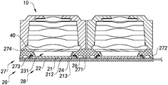
- Figure 3 is a cross-sectional view of a photosensitive member in accordance with a first preferred embodiment of the present invention.
- Figure 4 is a schematic illustration of the manufacturing process of a photosensitive member in accordance with a first preferred embodiment of the present invention.
- Figure 5 is a schematic view showing a method of manufacturing a photosensitive member in accordance with a first preferred embodiment of the present invention.
- 6A and 6B are cross-sectional views of different camera modules in accordance with a first preferred embodiment of the present invention.
- 7A, 7B and 7C are different embodiments of a motor connection structure of a photosensitive member in accordance with a first preferred embodiment of the present invention.
- Figure 8 is a cross-sectional view of another camera module in accordance with a first preferred embodiment of the present invention.
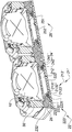
- FIG. 9 is a cross-sectional view of an array camera module and a photosensitive member thereof in accordance with a second preferred embodiment of the present invention.
- 10A through 10C are respectively cross-sectional views of three different embodiments of an array camera module and a photosensitive member thereof according to a third preferred embodiment of the present invention.
- Figure 11 is a cross-sectional view showing an array camera module and a photosensitive member thereof according to a fourth preferred embodiment of the present invention.
- Figure 12 is a cross-sectional view showing an array camera module and a photosensitive member thereof in accordance with a fifth preferred embodiment of the present invention.
- Figure 13 is a cross-sectional view showing an array camera module and a photosensitive member thereof in accordance with a sixth preferred embodiment of the present invention.
- Figure 14 is a cross-sectional view showing an array camera module and a photosensitive member thereof according to a seventh preferred embodiment of the present invention.
- Figure 15 is a cross-sectional view showing an array camera module and a photosensitive member thereof according to an eighth preferred embodiment of the present invention.
- Figure 16 is a schematic view showing a method of manufacturing a photosensitive member according to the above preferred embodiment of the present invention.
- Figure 17 is a cross-sectional view showing a camera module and a photosensitive member thereof according to a ninth preferred embodiment of the present invention.
- FIG. 18 is a perspective, cross-sectional view showing one of the steps of manufacturing an array camera module according to a preferred embodiment of the present invention, wherein the photosensitive element of the array camera module is mounted on a chip mounting area of the circuit board. And the chip connector of the photosensitive element and the circuit board connector of the circuit board are connected by a set of leads, wherein the circuit board is an integrated circuit board.
- FIG. 19 is a perspective, cross-sectional view showing the second step of the manufacturing process of the array camera module according to the above preferred embodiment of the present invention, wherein a support body of the array camera module is disposed to cover the photosensitive element. At least a portion of the non-photosensitive area to form a molded photosensitive member semi-finished product.
- 20A is a perspective, cross-sectional view showing the third step of the manufacturing process of the array camera module according to the above preferred embodiment of the present invention, wherein the molded photosensitive member semi-finished product is placed on an upper mold of a molding die and Between the dies, and the nip of the upper mold is in contact with the top surface of the support body.
- FIG. 20B is a perspective, cross-sectional view showing a modified embodiment of the third embodiment of the array camera module according to the above preferred embodiment of the present invention, wherein a cover film is disposed on the pressing surface of the upper mold, The cover film is located between the pressing surface of the upper mold and the top surface of the support body when the pressing surface of the upper mold is pressed against the top surface of the support body.
- Figure 21 is a perspective, cross-sectional view showing the fourth step of the manufacturing process of the array camera module according to the above preferred embodiment of the present invention, wherein a molding material is added to the molding formed between the upper mold and the lower mold. space.
- FIG. 22 is a perspective, cross-sectional view showing the fifth step of the manufacturing process of the array camera module according to the above preferred embodiment of the present invention, wherein a molding sensitization of the array camera module is formed after the molding material is cured. Component.
- FIG. 23 is a perspective cross-sectional view showing the sixth manufacturing step of the array camera module according to the above preferred embodiment of the present invention, wherein a filter element of the array camera module is assembled to the molding base. The top surface of the seat.
- FIG. 24 is a perspective, cross-sectional view showing the seventh manufacturing step of the array camera module according to the above preferred embodiment of the present invention, wherein an optical lens of the array camera module is assembled to a driver, the driver It is assembled to the top surface of the molded base.
- 25 is a perspective, cross-sectional view showing a modified embodiment of the array camera module according to the above preferred embodiment of the present invention, wherein each of the drivers is mounted on a bracket of the array camera module. Each installation space is formed to form the array camera module.
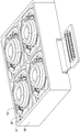
- FIG. 26 is a perspective view of the array camera module according to the above preferred embodiment of the present invention.
- FIG. 27 is a perspective view showing a first modified embodiment of the array camera module according to the above preferred embodiment of the present invention.
- FIG. 28 is a perspective, cross-sectional view showing a second modified embodiment of the array camera module according to the above preferred embodiment of the present invention.
- FIG. 29 is a perspective, cross-sectional view showing a third modified embodiment of the array camera module according to the above preferred embodiment of the present invention.
- Figure 30 is a perspective, cross-sectional view showing a fourth modified embodiment of the array camera module according to the above preferred embodiment of the present invention.
- Figure 31 is a perspective, cross-sectional view showing a fifth modified embodiment of the array camera module according to the above preferred embodiment of the present invention.
- FIG. 32 is a perspective cross-sectional view showing a sixth modified embodiment of the array camera module according to the above preferred embodiment of the present invention.
- Figure 33 is a perspective, cross-sectional view showing a seventh modified embodiment of the array camera module according to the above preferred embodiment of the present invention.
- Figure 34 is a perspective, cross-sectional view showing an eighth modified embodiment of the array camera module according to the above preferred embodiment of the present invention.
- FIG. 35 is a perspective, cross-sectional view showing a ninth modified embodiment of the array camera module according to the above preferred embodiment of the present invention.
- FIG. 35B is a perspective, cross-sectional view showing a tenth modified embodiment of the array camera module according to the above preferred embodiment of the present invention.
- 36A is a perspective view showing a first modified embodiment of the molded photosensitive member semi-finished product of the array camera module according to the above preferred embodiment of the present invention, wherein the support body covers the circuit board. At least a portion of the edge region and at least a portion of the chip outer portion of the non-photosensitive region of the photosensitive element, the chip connection portion, and the chip inner portion.
- 36B is a perspective view showing a second modified embodiment of the molded photosensitive member semi-finished product of the array camera module according to the above preferred embodiment of the present invention, wherein the support body covers the circuit board. At least a portion of the edge region and at least a portion of the chip outer portion of the non-photosensitive region of the photosensitive element and the chip connection portion.
- 36C is a perspective view showing a third modified embodiment of the molded photosensitive member semi-finished product of the array camera module according to the above preferred embodiment of the present invention, wherein the support body covers the circuit board. At least a portion of the edge region and at least a portion of the chip outer portion of the non-photosensitive region of the photosensitive element.
- 36D is a perspective view showing a fourth modified embodiment of the molded photosensitive member semi-finished product of the array camera module according to the above preferred embodiment of the present invention, wherein the support body covers the circuit board. At least a portion of the edge region.
- 36E is a perspective view showing a fifth modified embodiment of the molded photosensitive member semi-finished product of the array camera module according to the above preferred embodiment of the present invention, wherein the support body covers the circuit board. At least a portion of the edge region.
- Figure 37 is a cross-sectional view showing a modified embodiment of the molded photosensitive member of the array camera module according to the above preferred embodiment of the present invention, wherein the molded base covers the outer side of the support body .
- 38 is a perspective, cross-sectional view of an array of camera modules in accordance with another preferred embodiment of the present invention.
- 39 is a perspective, cross-sectional view of an array of image pickup modules in accordance with another preferred embodiment of the present invention.
- FIG. 40 is a perspective, cross-sectional view of an array of image pickup modules in accordance with another preferred embodiment of the present invention.
- 41 is a perspective, cross-sectional view of an array of camera modules in accordance with another preferred embodiment of the present invention.
- FIG. 42 is a perspective, cross-sectional view of an array of image pickup modules in accordance with another preferred embodiment of the present invention.
- 43 is a schematic diagram of an electronic device with the array camera module of the above preferred embodiment of the present invention.
- a molded photosensitive member and an array image pickup module according to a first preferred embodiment of the present invention.
- the molded photosensitive member 20 is used for assembling and manufacturing the array camera module, thereby obtaining a molded type camera module.
- the molded photosensitive member 20 includes a joint package portion 27 and a photosensitive portion 28, and the joint package portion 27 is integrally connected to the photosensitive portion 28, such as moldedly connected to the photosensitive portion 28.
- the photosensitive portion 28 includes a wiring board 22 and at least two photosensitive elements 21, and each of the photosensitive elements 21 is disposed on the wiring board 22.
- the photosensitive member 21 is moldedly connected to the wiring board 22. More specifically, the joint package portion 27 is molded and attached to the photosensitive portion 28 by molding in a mold (Molding on Chip, MOC).
- the joint encapsulation portion 27 forms two light windows 231 such that the joint encapsulation portions 27 surround the respective photosensitive members The outer side of the 21, and the light path of each of the optical lens 10 and the corresponding photosensitive element 21 is provided.
- Each of the photosensitive elements 21 is disposed on the wiring board 22 at a position corresponding to each of the optical windows 231.
- the joint encapsulation portion 27 includes a connecting body 271 and two outer ring bodies 272, and the connecting body 271 is integrally molded integrally between the two outer ring bodies 272, and the outer ring is separated into adjacent
- the two parts form two light windows 231, and the two photosensitive elements 21 are located on both sides of the connecting body 271, so as to be suitable for assembling the array camera module.
- the connecting body 271 is a common part of the two optical lenses 10, that is, when the optical lens 10 is mounted, each of the optical lenses 10 occupies a corresponding portion of the connecting body 271.
- the photosensitive portion 28 includes a connection line (not shown) and at least one electronic component 26.
- the connecting line is preset on the circuit board 22, and the electronic component 26 is electrically connected to the connecting line and the photosensitive element 21 for the photosensitive operation process of the photosensitive element 21.
- the electronic component 26 is convexly disposed on the circuit board 22 .
- the electronic component 26 can be, for example but not limited to, a resistor, a capacitor, a diode, a triode, a potentiometer, a relay or a driver, and the like.
- the connected package 27 encapsulates the electronic component 26 inside, so that the electronic component 26 is not directly exposed to the space, more specifically, is not exposed.
- the electronic component 26 In the environment in contact with the photosensitive element 21, when assembled into the array camera module, the electronic component 26 is not contaminated with dust or the like, and does not affect the photosensitive element 21,
- the electronic component 26 In the conventional camera module, the electronic component 26 is exposed in a manner such as a resisting container member, thereby preventing dust and debris from staying on the surface of the electronic component 26 by molding and covering, thereby avoiding contamination of the photosensitive member 21.
- the camera module has a bad phenomenon such as black spots.
- the electronic component 26 is protruded from the circuit board 22 as an example.
- the electronic component 26 is embedded in the The inside of the circuit board 22, without protruding from the circuit board 22, it will be understood by those skilled in the art that the structure, type and location of the electronic components 26 are not a limitation of the present invention.
- the electronic components 26 can be protruded between the two photosensitive elements 21, which can be covered by the connecting body 271, so that no additional need for the lens holder in the conventional array module is required.
- the installation space is such that the size of the array camera module of the present invention is reduced.
- the photosensitive portion 28 includes a plurality of leads 24 for electrically connecting the photosensitive members 21 and the wiring board 22.
- each of the leads 24 can be implemented, specifically, but not necessarily limited to, a gold wire, a copper wire, an aluminum wire, a silver wire, or the like.
- the lead wires 24 may be connected to the photosensitive member 21 and the wiring board 22 in an arc shape.
- each of the leads 24 is molded inside the connected package portion 27 so that each of the leads 24 can be covered by the joint package portion 27 without being directly exposed to Externally, when assembling the array camera module, the lead wires 24 are not subjected to any contact damage, and the influence of environmental factors on the leads 24, such as temperature, is caused, so that the photosensitive elements 21 and the The communication connection between the circuit boards 22 is stable, which is completely different from the prior art.
- the bottom of the light window 231 of the connected package portion 27 may have an inclined shape that gradually increases from bottom to top.
- the connected package 27 encloses the electronic component 26 and the lead 24, and has the camera module for protecting the electronic component 26 and the lead 24 and obtaining more performance.
- the conjoined package portion 27 is not limited to encasing the electronic component 26 or the lead 24 . That is, in other embodiments of the present invention, the joint package portion 27 may be directly molded to the circuit board 22 of the electronic component 26 without protruding, or may be molded in the Different positions such as the outer side and the periphery of the electronic component 26 are provided.
- the photosensitive element 21 has a photosensitive area 212 and a non-sensitive area 213, and the non-sensitive area 213 surrounds the periphery of the photosensitive area 212.
- the photosensitive region 212 is used for photoreceptive action, and the lead 24 is connected to the non-photosensitive region 213.
- the joint encapsulation portion 27 extends over the non-photosensitive region 213 of the photosensitive member 21, thereby laminating the photosensitive member 21 to the line by molding. Board 22.
- the in-mold moldable range of the joint package portion 27 is expanded by, for example, molding on a chip (MOC).
- MOC molding on a chip
- the conjoined package portion 27 is convexly surrounding the outside of the photosensitive region 212 of the photosensitive member 21, in particular, the conjoined package portion 27 is integrally closedly connected, such that It has a good seal so that when the molded photosensitive member 20 is used to assemble the array camera module, the photosensitive member 21 is sealed inside to form a closed inner space.
- a conventional wiring board may be selected as the wiring board 22, and the two photosensitive elements 21 are disposed on the wiring board 22, For example, attaching each of the photosensitive elements 21 to the circuit board 22, and electrically connecting the photosensitive elements 21 through the leads 24, such as a gold wire, and then the circuit board 22 after preliminary assembly.
- the photosensitive element 21 is integrally packaged on the component, for example, by molding, and the circuit board after the SMT process (Surface Mount Technology surface mount process) is molded by an injection molding machine by an insert molding process.
- the joint package portion 27 is formed by the joint package portion 27 or by a molding process commonly used in a semiconductor package.
- the circuit board 22 can be selected, for example, but not limited to, a soft and hard bonding board, a ceramic substrate (without a soft board), a PCB hard board (without a soft board), and the like.
- the manner in which the conjoined package portion 27 is formed may be selected, for example, but not limited to, an injection molding process, a molding process, and the like.
- the material that can be selected for the joint encapsulation portion 27 is, for example, but not limited to, nylon, LCP (Liquid Crystal Polymer), PP (Polypropylene, polypropylene), etc., and the molding process can be selected. Resin is used.
- the connected package portion 27 includes a covering portion 273 and a filter element mounting portion 274, and the filter element mounting portion 274 is integrally molded integrally connected to the covering portion 273, the covering portion 273 is molded and attached to the wiring board 22 for covering the electronic component 26 and the lead wires 24.
- the filter element mounting section 274 is used to mount the filter element 40, that is, when the molded photosensitive component 20 is used to assemble the array camera module, the filter of the array camera module
- the light element 40 is mounted to the filter element mounting section 274 such that the filter element 40 is located on the photosensitive path of the photosensitive element 21 and does not require the provision of an additional filter element 40 mounting bracket.
- the joint package portion 27 has the function of a conventional bracket here, but based on the advantage of the molding process, the top of the filter element mounting portion 274 can be made to have a good process by means of a mold process.
- the flatness is such that the filter element 40 is mounted flat, which is also superior to the conventional camera module.
- the filter element mounting portion 274 has two mounting slots 2741, and each of the mounting slots 2741 communicates with the corresponding light window 231 to provide sufficient installation space for the two filter elements 40, respectively.
- the filter element 40 does not protrude from the top surface of the filter element mounting section 274. That is, the joint encapsulation portion 27 is provided with two mounting grooves 2741 to facilitate mounting the filter elements 40 to the conjoined package portion 27, and the respective filters are not convex. Out of the connected package portion 27.
- the filter element 40 is an infrared cut filter IRCF.
- the mounting groove 2741 can be used to mount the filter element 40, while in other implementations of the invention, the mounting groove 2741 can be used to mount the device.
- the components of the motor or the lens barrel of the array camera module, those skilled in the art should understand that the shape and use of the mounting groove 2741 are not limited by the present invention.
- the inner wall of the joint package portion 27 may be disposed according to the shape of the lead wire 24, such as being inclined, so that the joint package portion is made while covering the lead wire 24.
- the inner wall of 27 reflects less stray light to improve the imaging quality of the array camera module. It will be understood by those skilled in the art that the shape of the conjoined package portion 27 is not a limitation of the present invention.
- the molded photosensitive member 20 includes at least two motor connection structures 29, each of which is coupled to a driver 30 of the array camera module.
- the driver 30 has at least one motor pin 31.
- Each of the motor connecting structures 29 includes at least one first connecting line 291, and each of the first connecting lines 291 is used for The driver 30 and the circuit board 22 are electrically connected.
- Each of the first connecting lines 291 is electrically connected to the circuit board 22.
- the first connection line 291 is electrically connected to the connection circuit of the circuit board 22.
- the first connection line 291 is disposed on the connected package portion 27 and extends to the top end of the connected package portion 27.
- the first connecting line 291 includes a motor connecting end 2911 exposed at the top end of the connected package portion 27 for electrically connecting the motor pin 31 of the driver 30. It is worth mentioning that the first connecting line 291 can be disposed in an embedded manner when the connected package portion 27 is formed. In the conventional connection method, components such as a drive motor are connected to the wiring board by providing separate wires, and the manufacturing process is relatively complicated, and the manner of embedding the first connection line 291 at the time of molding of the present invention is It can replace the traditional motor welding and other processes, and make the circuit connection more stable.
- the first connecting line 291 is a wire embedded in the inside of the connected package portion 27.
- the motor pin 31 may be connected to the motor connection end 2911 through an anisotropic conductive film, or may be connected to the motor connection end 2911 by soldering.
- the buried position of the first connecting line 291 and the position of the motor connecting end 2911 of the first connecting line 291 displayed on the connected package portion 27 can be set as needed, for example,
- the motor connection end 2911 of the first connection line 291 may be disposed at a periphery of the conjoined package portion 27, that is, a top surface of the conjoined package portion 27,
- the top surface of the filter element mounting portion 274 and in another embodiment of the present invention, the motor connection end 2911 may be disposed in the inner circumference of the conjoined package portion 27, that is, the conjoined package portion 27
- the bottom surface of the mounting groove 2741 can provide different mounting positions of the driver 30.
- the motor connection end 2911 is disposed on the peripheral top surface of the conjoined package portion 27, when the driver 30 needs to be mounted to the office
- the motor connection end 2911 is disposed in the inner circumference of the connected package portion 27, that is, the bottom surface of the mounting groove 2741.
- the photosensitive member 21 is attached to the photosensitive member 21, and then the MOP is molded on the wiring board 22 and the photosensitive member 21.
- the first package line 291 is disposed inside the joint package portion 27 in a buried manner during molding, and the first connection line 291 is electrically connected to the circuit board 22
- the motor connection end 2911 of the first connecting line 291 is displayed on the top end of the connected package portion to facilitate connection to the motor pin 31 of the driver 30.
- each of the motor pins 31 of the driver 30 is connected to the first connecting line 291 by soldering.
- a motor connection end 2911 such that the driver 30 is electrically connected to the circuit board 22, and there is no need to provide a separate wire to connect the driver 30 and the circuit board 22, and the said driver 30 is The length of the motor pin 31 can be reduced.
- a camera module may be an automatic focus camera module (AFCM).
- the array camera module includes a molded photosensitive component 20, two filter elements 40, two of the drivers 30, and two of the optical lenses 10.
- Each of the filter elements 40 is mounted to the molded photosensitive member 20, and each of the optical lenses 10 is mounted to each of the drivers 30, and each of the drivers 30 is mounted on the molded photosensitive member 20.
- the filter element 40 is mounted to the mounting groove 2741 of the filter element mounting section 274 of the joint package portion 27 of the molded photosensitive member 20.
- Each of the drivers 30 is mounted on the top end of the filter element mounting section 274 of the joint package portion 27 of the molded photosensitive member 20.
- the motor pin 31 of the driver 30 is electrically connected to the motor connection end 2911 of the motor connection structure 29, thereby being electrically connected to the circuit board 22 through the motor connection structure 29.
- the motor connection structure 29 includes a first lead slot 292 for receiving the motor pin 31 of the driver 30 of the array camera module.
- the first lead slot 292 is disposed at an upper end of the connected package portion 27.
- the motor connecting structure 29 includes at least one second connecting line 293, and each of the second connecting lines 293 is used for electrically connecting the driver 30 and the The circuit board 22 is described.
- the second connecting line 293 is disposed on the connected package portion 27 and extends upward to the bottom wall of the first lead slot 292 of the connected package portion 27.
- the second connecting line 293 includes a second motor connecting end 2931 exposed on the bottom wall of the first pin slot 292 of the connected package portion 27 for electrically connecting the driver 30 Motor pin 31.
- the second motor connection end 2931 can be implemented as a pad.
- the second connecting line 293 can be implemented as a wire embedded in the inside of the connected package portion 27.
- the photosensitive member 21 is first mounted, and then the connected package is molded in MOC manner on the wiring board 22 and the photosensitive member 21.
- a portion 27, and presets the first lead slot 292 of a predetermined length, and the second connecting line 293 can be disposed in an embedded manner during molding, and the second connecting line 293 is electrically connected to the line a plate 22, and the second motor connection end 2931 of the second connection line 293 is displayed on a bottom wall of the first pin slot 292 of the conjoined package portion 27 to facilitate connection to the The motor pin 31 of the driver 30.
- each of the motor pins 31 of the driver 30 is inserted into the first lead groove 292 and connected by soldering.
- the connection is made such that the motor pins 31 of the driver 30 can be stably connected to prevent externally undesired contact with the motor pins 31.
- the second connecting line 293 can be implemented as a wire embedded in the inside of the connected package portion 27.
- the motor connection structure 29 includes a second lead slot 294 for receiving the motor pin 31 of the driver 30 of the array camera module.
- the second lead slot 294 is disposed in the connected package portion 27.
- the motor connection structure 29 includes at least one circuit contact 295 that is preset to the circuit board 22 and electrically connected to the connection line of the circuit board 22. Further, each of the second lead slots 294 extends from the top end of the conjoined package portion 27 to the circuit board 22, and causes the circuit contacts 295 to be displayed.
- the motor pin 31 is inserted into the second pin slot 294 and may be soldered to the circuit contact 295.
- each of the circuit contacts 295 is preset on the wiring board 22, thereby mounting the photosensitive member 21, and then on the wiring board 22 and the On the photosensitive element 21, the connected package portion 27 is molded in an MOC manner, and the second lead slot 294 of a predetermined length is preset, and the circuit contact 295 is passed through the second lead slot 294. Displayed to facilitate connection to the motor pin 31 of the driver 30.
- each of the motor pins 31 of the driver 30 is inserted into the second lead groove 294 and connected by soldering.
- the circuit contacts 295 on the circuit board 22 such that the driver 30 is electrically connected to the circuit board 22, and the motor pins 31 of the driver 30 can be stably connected to prevent external need Touching the motor pin 31.
- the motor connection structure 29 includes an engraving line 296 for electrically connecting the connection line on the circuit board 22, the photosensitive element 21, and a motor.
- the engraving line 296 can be disposed by way of Laser Direct Structuring (LDS) when forming the conjoined package portion 27.
- LDS Laser Direct Structuring
- components such as a drive motor are connected to the wiring board by providing separate wires, and the manufacturing process is relatively complicated, and the manner in which the engraving line 296 is provided at the time of molding of the present invention can be replaced.
- the engraving line 296 may be formed by first providing an engraving groove in the conjoined package portion 27, and then arranging the circuit in the engraving groove by electroplating.
- the manner in which the driver 30 of the array camera module is connected to the molded photosensitive member 20 is described by taking the connection manner of the motor connection structure 29 as an example.
- the connection manner of the driver 30 can also be combined with the connection manner corresponding to FIG. 7A, 7B, and 7C.
- the driver 30 can be in a conventional manner. It is attached to the molded photosensitive member 20, such as by soldering. It will be understood by those skilled in the art that the manner in which the driver 30 and the molded photosensitive member 20 are attached is not a limitation of the present invention.
- the array camera module can be a certain focus module.
- the array camera module includes a molded photosensitive component 20, two of the filter elements 40, and two of the optical lenses 10.
- Each of the filter elements 40 is mounted to the molded photosensitive member 20, and each of the optical lenses 10 is mounted on the molded photosensitive member 20.
- each of the filter elements 40 is mounted to the mounting groove 2741 of each of the filter element mounting sections 274 of the joint package portion 27 of the molded photosensitive member 20.
- Each of the optical lenses 10 is mounted on the top of the joint package portion 27 of the molded photosensitive member 20.
- each of the optical lenses 10 is mounted on the top end of the connected package portion 27 of the molded photosensitive member 20, so that the connected package portion 27 is equivalent to that in the conventional camera module.
- the function of the bracket provides a support and fixed position for the optical lens 10, but the assembly is different from the conventional COB process.
- the bracket of the camera module of the conventional COB process is fixed to the circuit board in a pasting manner, and the joint package portion 27 is fixed to the circuit board 22 by a molding process, and the fixing process is not required, and the molding method is relatively pasted.
- the fixing has better connection stability and controllability of the process, and the connected package portion 27 and the electronic component 26 mounted on the circuit board 22 are in the joint package portion.
- the connected package portion 27 encloses the electronic component 26 and the
- the lead wires 24 enable the conventional bracket function and the electronic component 26 and the lead wires 24 to be spatially overlapped, without requiring a safety distance around the circuit device like a conventional camera module, thereby enabling the bracket function
- the height of the package portion 27 can be set to a small range, thereby further providing a space in which the thickness of the camera module can be reduced.
- the joint encapsulation portion 27 replaces the conventional bracket, avoiding the tilt error caused by the bracket during the assembly and assembly, and reducing the cumulative tolerance of the assembly of the camera module.
- joint encapsulation portion 27 covers the lead wire 24, and the joint encapsulation portion 27 extends to the non-photosensitive region 213 of the photosensitive member 21, so that the conjoined package portion 27 can be contracted inward, thereby Further reducing the lateral length and width dimensions of the array camera module.
- the circuit board 22H has two inner recesses 2222H, and each of the photosensitive elements 21 is disposed in the inner recess 2222H, thereby causing the photosensitive element 21 and the wiring board
- the relative height of 22H is lowered, so that when the joint package portion 27 covers the photosensitive member 21, the height requirement for the joint package portion 27 is reduced, thereby reducing the assembly of the molded photosensitive member 20.
- the height of the array camera module is the height of the array camera module.
- FIG. 10A it is an embodiment of an array camera module and a photosensitive member thereof according to a third preferred embodiment of the present invention.
- the photosensitive portion 28 of the molded photosensitive member 20 includes a reinforcing layer 280I, and the reinforcing layer 280I is laminatedly connected to the wiring.
- the bottom layer of the board 22 is used to enhance the structural strength of the circuit board 22. That is, the reinforcing layer 280I is placed on the underlayer encapsulation portion 27 and the region where the photosensitive member 21 is located on the circuit board 22, so that the circuit board 22 stably and reliably supports the connection.
- the body package portion 27 and the photosensitive element 21 is used to enhance the structural strength of the circuit board 22.
- the reinforcing layer 280I is a metal plate attached to the bottom layer of the circuit board 22 to increase the structural strength of the circuit board 22, and on the other hand, the molded photosensitive member 20 is increased.
- the heat dissipation performance can effectively dissipate the heat generated by the photosensitive element 21.
- the circuit board 22 can adopt an FPC (Flex Print Circuit), and the rigidity of the FPC by the reinforcement layer 280I enables the FPC with good bending performance to satisfy the requirements.
- the bearing requirements of the molded photosensitive member 20 are described. That is to say, the circuit board 22 has a wider range of options, such as a PCB (Printed Circuit Board), FPC, RG (Rigid Flex, soft and hard board).
- the structural strength of the wiring board 22 is increased by the reinforcing layer 280I and the heat dissipation performance is improved, so that the thickness of the wiring board 22 can be reduced, so that the molded photosensitive member
- the height of 20 is further reduced, and the height of the array camera module assembled therefrom is reduced.
- the circuit board 22 further has at least two receiving spaces 224, each of which is housed in the receiving space 224 of the circuit board 22, in such a manner, can be reduced
- the height difference between the upper surface of the photosensitive element 21 and the upper surface of the wiring board 22 is even such that the upper surface of the photosensitive element 21 and the upper surface of the wiring board 22 are in the same plane, thus enabling
- the height dimension of the array camera module is further reduced, so that the array camera module is particularly suitable for being applied to electronic devices that are thin and thin.
- the accommodation space 224 of the circuit board 22 may be implemented to accommodate a slot, and in this example specific example shown in FIG.
- the accommodation space 224 of the wiring board 22 may be implemented as a through hole, each of the photosensitive elements 21 being electrically connected to the wiring board 22, and each of the photosensitive elements 21 being accommodated in the wiring, respectively.
- the reinforcement layer 280I is disposed to overlap the lower side of the circuit board 22 to reinforce the circuit board 22.
- FIG. 11 there is shown a cross-sectional view of an array camera module and a photosensitive member thereof according to a fourth preferred embodiment of the present invention.
- the circuit board 22 has at least one reinforcing hole 220J, and the connected package portion extends into the reinforcing hole 220J, thereby enhancing the structural strength of the circuit board 22.
- the position of the reinforcing hole 220J can be selected according to needs, and is set according to the structural strength requirement of the circuit board, such as a symmetrical structure.
- the structural strength of the circuit board 22 is enhanced by the arrangement of the reinforcing holes 220J, so that the thickness of the circuit board 22 can be reduced, the thickness of the camera module assembled therefrom can be reduced, and the molding can be improved.
- the heat dissipation performance of the photosensitive member 20 can be selected according to needs, and is set according to the structural strength requirement of the circuit board, such as a symmetrical structure.
- the reinforcing hole 220J is in the shape of a groove, so that when the molded photosensitive member 20 is manufactured, the molding material of the joined portion is not leaked by the reinforcing hole 220J.
- FIG. 12 it is an array image pickup module and a molded photosensitive member 20 thereof according to a fifth preferred embodiment of the present invention.
- the circuit board 22 has at least one reinforcing hole 220K, and the connected package portion extends into the reinforcing hole 220K, thereby enhancing the structural strength of the circuit board 22.
- the position of the reinforcing hole 220K can be selected as needed, and is set according to the structural strength requirement of the circuit board, such as a symmetrical structure.
- the structural strength of the circuit board 22 is enhanced by the arrangement of the reinforcing holes 220K, so that the thickness of the circuit board 22 can be reduced, the thickness of the camera module assembled therefrom can be reduced, and the molding can be improved.
- the heat dissipation performance of the photosensitive member 20 can be selected as needed, and is set according to the structural strength requirement of the circuit board, such as a symmetrical structure.
- the reinforcing holes 220K are perforated, that is, pass through the circuit board 22 such that both sides of the circuit board 22 are communicated, thereby manufacturing the molded photosensitive member 20.
- the molding material of the joint package portion is sufficiently combined with the wiring board 22 to form a more robust composite material structure, and the perforation is easier to manufacture than the structure of the groove.
- FIG. 13 it is an array camera module and a photosensitive member thereof according to a sixth preferred embodiment of the present invention.
- the connected package portion 27L includes a covering portion 273L, a filter element mounting portion 274L, and a lens mounting portion 275L.
- the filter element mounting portion 274L and the lens mounting portion 275L are integrally molded and integrally connected to each other.
- the covering section 273L is molded and connected to the circuit board 22 for covering the electronic component 26 and the lead 24 .
- the filter element mounting section 274L is used to mount the two filter elements 40, that is, when the molded photosensitive component 20 is used to assemble the array camera module, the array camera module
- Each of the filter elements 40 is mounted to the filter element mounting section 274L such that each of the filter elements 40 is located on the photosensitive path of each of the photosensitive elements 21, and there is no need to provide an additional filter element 40 mounting bracket.
- the joint package portion 27L has the function of a conventional bracket here, but based on the advantage of the molding process, the top of the filter element mounting portion 274L can be made to have a good process by means of a mold process.
- the flatness is such that each of the filter elements 40 is mounted flat, which is also superior to the conventional array camera module.
- the lens mounting section 275L is used to mount the two optical lenses 10, that is, when the molded photosensitive component 20 is used to assemble the array camera module, each of the optical lenses 10 is mounted on the same.
- the inside of the lens mounting section 275L of the joint encapsulation portion 27L is provided to provide a stable mounting position for the optical lens 10.
- the joint encapsulation portion 27L includes a connecting body 271L and two outer ring bodies 272L integrally molded between the two outer ring bodies 272L and separating the outer rings into adjacent
- the two parts form two optical windows 231L, and the two chips are located on both sides of the connecting body 271L, so as to be suitable for assembling the array camera module.
- the connecting body 271L is a common part of the two optical lenses 10, that is, when the optical lens 10 is mounted, each of the optical lenses 10 occupies a portion corresponding to the connecting body 271L.
- the filter element mounting portion 274L has two mounting grooves 2741L, and each of the mounting grooves 2741L communicates with the corresponding light window 231L to provide sufficient installation space for the filter element 40, so that the filter The light element 40 does not protrude from the top surface of the filter mounting section.
- the lens mounting section 275L has two lens mounting slots 2751L, and the lens mounting slots 2751L are connected to the corresponding light window 231L to provide sufficient mounting space for the optical lens 10.
- the filter element mounting section 274L and the lens mounting section 275L integrally extend upwardly, and a stepped structure is formed inside to provide a support fixing position for the filter element 40 and the optical lens 10, respectively. There is thus no need to provide additional components to mount the filter element 40 and the optical lens 10.
- the lens mounting section 275L has two lens inner walls 2752L, and the lens inner wall 2752L has a closed annular shape, and is adapted to provide a mounting space for each of the optical lenses 10, respectively. It is worth mentioning that the lens inner wall 2752L of the lens mounting section 275L has a flat surface, so as to be suitable for mounting the unthreaded optical lens 10 to form a fixed focus module. In particular, the optical lens 10 can be fixed to the lens mounting section 275L by bonding.
- the molded photosensitive member 20 includes a shield layer 290 that wraps the wiring board 22 and the joint package portion 27, thereby reinforcing the wiring board 22 At the same time as the structural strength, the electromagnetic interference resistance of the molded photosensitive member 20 is enhanced.
- the array camera module includes a molded photosensitive member 20N.
- the optical lens 10 is mounted on the molded photosensitive member 20N and assembled to form the array camera module.
- the optical lens 10 can be fixed to the top end of the joint package portion 27N of the molded photosensitive member 20N by adhesive bonding, and the joint body is made by the characteristics of mold manufacturing in the molding process.
- the top end of the package portion 27N has a good flatness, and provides good mounting conditions for the optical lens 10, thereby obtaining a high quality camera module.
- the molded photosensitive member 20N is used for assembling and manufacturing the array camera module, thereby obtaining a molded type camera module.
- the molded photosensitive member 20N includes a joint package portion 27N and a photosensitive portion 28N, and the joint package portion 27N is moldedly coupled to the photosensitive portion 28N.
- the circuit board portion includes a circuit board 22N, and the joint package portion 27N forms two light windows 231N such that the joint package portions 27N surround the outer sides of the photosensitive elements 21N, respectively, and provide the respective opticals.
- Each of the photosensitive elements 21N is provided on the wiring board 22N at a position corresponding to each of the optical windows 231N.
- the joint encapsulation portion 27N includes a connecting body 271N and two outer ring bodies 272N integrally molded between the two outer ring bodies 272N and separating the outer ring body 272N into Two adjacent light windows 231N are formed, and the two photosensitive elements 21N are located on both sides of the connecting body 271N, so as to be suitable for assembling the array camera module.
- the connecting body 271N is a common portion of the two drivers 30, that is, when each of the drivers 30 is assembled to the connected package portion 27N of the sochin molded photosensitive member 20N, respectively.
- a part of the two actuators 30 are assembled at different positions of the connecting body 271N.
- the photosensitive portion 28N includes a wiring board 22N and two photosensitive elements 21N, and each of the photosensitive elements 21N is disposed on the wiring board 22N. According to this embodiment of the invention, the photosensitive member 21N is moldedly connected to the wiring board 22.
- the photosensitive portion 28N includes a connection line (not shown) and at least one electronic component 26N.
- the connection line is preset to the circuit board 22N, and the electronic component 26N is electrically connected to the connection line and the photosensitive element 21N for the photosensitive operation process of the photosensitive element 21N.
- the electronic component 26N is convexly It is disposed on the circuit board 22N.
- the electronic component 26N can be, for example but not limited to, a resistor, a capacitor, a diode, a triode, a potentiometer, a relay or a driver, and the like.
- the connected package portion 27N encapsulates the electronic component 26N therein, so that the electronic component 26N is not directly exposed to the space, more specifically, is not exposed.
- the electronic component 26N In an environment in which the photosensitive element 21N is in communication, when assembled into the array camera module, the electronic component 26N is not contaminated with dust or the like, and does not affect the photosensitive element 21N.
- the electronic component 26N In the conventional camera module, the electronic component 26N is exposed in a manner such as a resisting container member, thereby preventing dust and debris from staying on the surface of the electronic component 26N by molding and covering, thereby avoiding contamination of the photosensitive member 21N.
- the camera module has a bad phenomenon such as black spots.
- the photosensitive portion 28N includes a plurality of leads 24N for electrically connecting the photosensitive members 21N and the wiring board 22N.
- each of the leads 24N may be implemented, specifically, but not necessarily limited to, a gold wire, a copper wire, an aluminum wire, a silver wire, or the like.
- each of the leads 24N is molded inside the connected package portion 27N so that each of the leads 24N can be covered by the joint encapsulation portion 27N without being directly exposed to Externally, when assembling the array camera module, the lead 24N is not subjected to any touch damage, and the influence of environmental factors on the lead 24N, such as temperature, is caused, so that the photosensitive element 21N and the The communication connection between the circuit boards 22N is stable, which is not provided at all in the prior art.
- the connected package portion 27N covers the electronic component 26N and the lead wire 24N, and has the camera module for protecting the electronic component 26N and the lead wire 24N and obtaining more performance.
- the conjoined package portion 27N is not limited to encapsulating the electronic component 26N or the lead 24N. That is, in other embodiments of the present invention, the joint encapsulation portion 27N may be directly molded to the wiring board 22N of the electronic component 26N that is not protruding, or may be molded in the Different positions such as the outer side and the periphery of the electronic component 26N.
- the photosensitive element 21N has a photosensitive area 212N and a non-sensitive area 213N, and the non-sensitive area 213N surrounds the periphery of the photosensitive area 212N.
- the photosensitive region 212N is used for photoreaction, and the lead 24N is connected to the non-photosensitive region 213N.
- the joint encapsulation portion 27N extends over the non-photosensitive region 213N of the photosensitive member 21N, thereby laminating the photosensitive member 21N to the line by molding. Plate 22N.
- the molding on chip for example, enlarges the inward moldable range of the joint package portion 27N, so that the wiring board 22N and the joint package can be reduced.
- the outer structural portion of the portion 27N further reduces the length and width dimensions of the molded photosensitive portion 28N, and reduces the length and width dimensions of the array camera module assembled therefrom.
- the molded photosensitive member 20N further includes two filter elements 40N, each of which is moldedly laminated on the corresponding photosensitive element 21N. An edge of each of the filter elements 40N is molded to the joint package portion 27N to fix the filter element 40N. It is worth mentioning that the filter element 40N covers the photosensitive element 21N, and isolates the photosensitive element 21N from the external environment to protect the photosensitive element 21N from damage.
- the photosensitive member 21N is attached to the wiring board 22N, and the lead 24N is connected to the photosensitive member 21N and the wiring board 22N, thereby
- the filter element 40N is attached to the photosensitive element 21N, and further, the wiring board 22N, the photosensitive element 21N, and the filter element 40N are molded to form the connected package portion 27N.
- the filter element 40N is overlaid on the photosensitive element 21N, damage of the molded mold to the photosensitive element 21N can be prevented, and since the filter element 40N and the photosensitive element The distance of 21N is reduced, so that the back focal length of the camera module assembled therefrom can be reduced, thereby reducing the height of the array camera module, and on the other hand, since it is not necessary to provide additional for the filter element 40N
- the support member thus also further reduces the thickness of the array camera module to a certain extent.
- the connected package portion 27N is convexly surrounding the outer side of the photosensitive region 212N of each of the photosensitive elements 21N, and in particular, the connected package portion 27N is integrally closed and connected. Providing good sealing properties, so that when the molded photosensitive member 20N is used to assemble the array camera module, the photosensitive member 21N is sealed therein The part forms a closed inner space.
- a conventional wiring board can be selected as the wiring board 22N, and the photosensitive member 21N is disposed on the wiring board 22N, and the photosensitive member 21N is passed.
- the lead wires 24N are electrically connected, and the filter elements 40N are further overlapped and attached to the corresponding photosensitive elements 21N, and further molded on the molded circuit board 22N and the photosensitive element 21N components after preliminary assembly.
- Molding such as using an injection molding machine, molding a circuit board after performing an SMT process (Surface Mount Technology surface mount process) to form the joint package portion 27N, or commonly used in a semiconductor package by an insert molding process (Insert Molding) process The molding process forms the joint package portion 27N.
- the circuit board 22N may be selected, for example, but not limited to, a soft and hard bonding board, a ceramic substrate (without a soft board), a PCB hard board (without a soft board), and the like.
- the manner in which the joint encapsulation portion 27N is formed may be selected, for example, but not limited to, an injection molding process, a molding process, and the like.
- the material of the joint encapsulation portion 27N can be selected, for example, but not limited to, nylon, LCP (Liquid Crystal Polymer), PP (Polypropylene, polypropylene), etc., and the molding process can be selected. Resin is used. It should be understood by those skilled in the art that the foregoing alternatives and the materials that can be selected are merely illustrative of the embodiments of the invention and are not intended to be limiting.
- the array camera module includes at least one support member 70 for mounting each of the filter elements 40, each of the optical lenses 10 or each of the drivers 30.
- the support member 70 is mounted to the joint package portion 27, and each of the filter elements 40 is mounted to the support member 70, and each of the drivers 30 is mounted to the Support 70.
- the specific shape of the support member 70 can be set as needed, such as providing a boss to facilitate mounting of each of the filters.
- the support member 70 shown may be a one-piece bracket, that is, a plurality of the filter elements 40 may be mounted at a time, or a single bracket, that is, one of the filter elements 40 may be mounted.
- the support member 70 is preferably a joint bracket. It will be understood by those skilled in the art that the specific shape of the support member 70 is not a limitation of the present invention.
- an array camera module according to another preferred embodiment of the present invention is illustrated, wherein the array camera module includes at least two optical lenses 10' and a molding The photosensitive member 20', wherein the molded photosensitive member 20' further includes at least two photosensitive members 21', a wiring board 22', a molding base 23', and at least two sets of leads 24'.
- Each of the photosensitive elements 21' includes a set of chip connectors 211', a photosensitive region 212', and a non-photosensitive region 213', wherein the photosensitive regions 212' and the non-sensitive regions 213' are integrally formed.
- the photosensitive area 212' is located in the middle of the photosensitive element 21'
- the non-sensitive area 213' is located outside the photosensitive element 21'
- the non-sensitive area 213' is around the photosensitive area 212'.
- the chip connector 211' is disposed in the non-photosensitive area 213'.
- the circuit board 22' includes at least two sets of circuit board connectors 221', at least two flat chip mounting areas 222', and an edge area 223', wherein the edge areas 223' and each of the chips
- the mounting area 222' is integrally formed, and the edge area 223' is located around each of the chip mounting areas 222', and the board connector 221' is disposed in the edge area 223'.
- Each of the leads 24' has a chip connection end 241' and a circuit board connection end 242', wherein the lead wire 24' is bent between the chip connection end 241' and the circuit board connection end 242'. Extend the ground.
- Each of the photosensitive elements 21' is respectively attached to each of the chip mounting regions 222' of the wiring board 22', wherein the chip connection end 241' of the leads 24' is connected to the The chip connector 211' of the photosensitive member 21', the circuit board connection end 242' of the lead 24' is connected to the circuit board connector 221' of the circuit board 22', the molding The pedestal 23' is integrally bonded at least to the edge region 223' of the wiring board 22' to form the molded photosensitive member 20', wherein each of the optical lenses 10' is respectively disposed on the mold The photosensitive path of each of the photosensitive elements 21' of the photosensitive photosensitive member 20'. Light reflected by the object enters the interior of the array camera module from each of the optical lenses 10' to be subsequently received and photoelectrically converted by the photosensitive region 212' of each of the photosensitive elements 21', thereby Get an image associated with the object.
- the chip connector 211 ′ of the photosensitive element 21 ′ and the circuit board connector 221 ′ of the circuit board 22 ′ may respectively be a lands That is, the chip connector 211' of the photosensitive element 21' and the circuit board connector 221' of the wiring board 22' may be in the shape of a disk for the said lead 24'
- the chip connection end 241' is connected to the chip connector 211' of the photosensitive element 21' and the said board connection end 242' of the lead 24' is connected to the circuit board 22' a circuit board connector 221'
- the chip connector 211' of the photosensitive element 21' and the circuit board connector of the circuit board 22' 221' may be respectively spherical, for example, solder paste or other solder material is spotted on the non-photosensitive region 213' of the photosensitive element 21' and the edge region 223' of the wiring board 22' to form a
- the chip connector 211' of the photosensitive element 21' and the circuit board connector 221' of the circuit board 22' do not constitute the present invention.
- a limitation of content and range that is, in other examples, the chip connector 211' of the photosensitive element 21' and the circuit board connector 221' of the circuit board 22' may have other such Illustrated shape.
- the non-photosensitive region 213' of the photosensitive element 21' further has a chip inner portion 2131', a chip connecting portion 2132', and a chip outer portion 2133', wherein the chip connector 211' is disposed on the a chip connecting portion 2132', the chip inner portion 2131' is circumferentially surrounding the photosensitive region 212', and both sides of the chip connecting portion 2132' respectively extend and are connected to the chip inner portion 2131' and the chip outer portion 2133'. That is, in the present invention, the region of the non-photosensitive region 213' from the position where the chip connector 211' is disposed to the edge position of the photosensitive region 212' is defined as the chip inner portion 2131.
- the area of the non-photosensitive area 213' where the chip connector 211' is disposed is defined as the chip connection portion 2132', and the non-photosensitive area 213' is set from the chip connector 211
- a region of the position to the outer edge of the photosensitive member 21' is defined as the chip outer portion 2133'.
- the photosensitive member 21' is, in order from the inside of the photosensitive member 21', the photosensitive region 212', the chip inner portion 2131', the chip connecting portion 2132', and the like from the inside to the outside.
- the chip outer portion 2133' is, in order from the inside of the photosensitive member 21', the photosensitive region 212', the chip inner portion 2131', the chip connecting portion 2132', and the like from the inside to the outside.
- the edge region 223' of the circuit board 22' further has a circuit board inner portion 2231', a circuit board connecting portion 2232', and a circuit board outer portion 2233', wherein the circuit board connector 221 'provided in the circuit board connecting portion 2232', the circuit board inner portion 2231' surrounds the chip mounting region 222', and both sides of the circuit board connecting portion 2232' extend and are connected to the The circuit board inner side portion 2231' and the circuit board outer side portion 2233'.
- the edge position of the edge region 223' from the position where the board connecting member 221' is disposed to the edge portion of the chip mounting region 222' is defined as the inner side portion of the wiring board 2231'
- the area of the edge area 223' where the circuit board connector 221' is disposed is defined as the circuit board connection portion 2232'
- the edge area 223' is connected from the circuit board to which the board is disposed
- the area of the member 221' to the outer edge of the wiring board 22' is defined as the outer side portion 2233' of the wiring board.
- the circuit board 22' is an integrated circuit board.
- each of the chip mounting areas 222' are symmetrically respectively.
- the two ends of the circuit board 22' are disposed such that the circuit board 22' forms a symmetrical structure.
- the type of the lead 24 ′ is not limited in the array camera module of the present invention.
- the lead 24 ′ may be implemented as a gold wire, that is, by a gold wire.
- the method can connect the photosensitive element 21' and the circuit board 22' together, so that after the optical signal is converted into an electrical signal by the photosensitive area 212' of the photosensitive element 21', the electrical signal It can be further transferred to the wiring board 22' through the lead 24'.
- the lead 24 ′ can also be implemented as any silver wire, copper wire or the like to enable the electrical signal to be implemented. The material is transferred between the photosensitive element 21' and the wiring board 22'.
- the array camera module can be a fixed focus camera module, or a zoom camera module, or a zoom camera module.
- the array camera module can be under the premise of being controlled by the height dimension. The ability to have auto focus and optical zoom to improve the image quality of the array camera module.
- the array camera module shown in FIG. 24 the array camera module further includes at least two drivers 30', wherein each of the optical lenses 10' is assembled to each of the drivers 30', and each of the drivers 30' is assembled The top surface of the molded base 23' is such that each of the optical lenses 10' is held on the photosensitive path of each of the photosensitive elements 21' of the molded photosensitive member 20', respectively.
- Each of the drivers 30' is electrically connected to the circuit board 22', respectively, to transmit power and control signals to each of the drivers 30' after the circuit board 22', each of the drivers 30'
- Each of the optical lenses 10' can be driven to move back and forth along the photosensitive path of each of the photosensitive elements 21', thereby adjusting the focal length of the array camera module. That is, the optical lens 10' can be drivingly disposed to the driver 30'.
- the type of the driver 30' is not limited in the array camera module of the present invention.
- the driver 30' may be implemented as any such as a voice coil motor.
- the array camera module further includes at least one filter element 40'.
- the array camera module may include one of the filter elements 40', wherein the filter element 40' is assembled to the top of the molded base 23' The surface is such that different positions of the filter element 40' correspond to the photosensitive paths of each of the photosensitive elements 21', respectively.
- the array camera module may include at least two of the filter elements 40', wherein each of the filter elements 40' is assembled to the molded base 23', respectively.
- each of the filter elements 40' respectively corresponds to a photosensitive path of each of the photosensitive elements 21', that is, each of the photosensitive elements 21', each of the array camera modules
- the filter element 40' and each of the optical lenses 10' have a one-to-one correspondence.
- the filter element 40' When the array camera module is used, light reflected by the object enters the interior of the array camera module from the optical lens 10', and can be filtered by the filter element 40'.
- the photosensitive element 21' receives and performs photoelectric conversion. That is, the filter element 40' is capable of filtering stray light, such as the infrared portion, in the light reflected by the object from the optical lens 10' into the array camera module, in such a manner The image quality of the array camera module can be improved.
- the filter element 40' may be directly assembled to the top surface of the molded base 23', or may be assembled by first assembling the filter element 40' to a support member. The components are assembled on the top surface of the molded base 23'. In this way, the size of the filter element 40' can be reduced to reduce the manufacturing cost of the array camera module.
- the filter elements 40' can be implemented in different types, for example, the filter elements 40' can be implemented as infrared A cut filter, a full transmissive spectral filter, and other filters or a combination of multiple filters, for example, the filter element 40' can be implemented as an infrared cut filter and a full transmissive filter. a combination of the infrared cut filter and the full transmissive spectral filter can be switched to be selectively located on the photosensitive path of the photosensitive element 21', for example, in an environment where light is sufficient during daylight hours.
- the infrared cut filter can be switched to the photosensitive path of the photosensitive element 21 ′ to filter the object entering the array camera module by the infrared cut filter. Infrared rays in the reflected light, when the array camera module is used in a dark environment such as at night, the full-transmission spectral filter can be switched to the photosensitive path of the photosensitive element 21' to allow Infrared part of the light into the camera module of the array is reflected by the object in transmission.
- the molded photosensitive member 20' further includes at least one support member 25' to protect the lead 24' and the photosensitive member 21' by the support member 25' when the molding process is performed.
- the number of support elements 25' is implemented as a minimum of two.
- the number of the support elements 25' is identical to the number of the photosensitive elements 21', each of the support elements 25' being provided to cover each of the described before the molding base 23' is formed
- the non-photosensitive region 213' of the photosensitive member 21' after the molding base 23' is molded, the molding base 23' covers the edge region 223' of the wiring board 22', A portion of the non-photosensitive region 213' of the photosensitive member 21' and a portion of the support member 25' to form the molded photosensitive member 20'.
- the support member 25' can effectively improve the array camera module Product yield and improved imaging quality of the array camera module.
- the number of support elements 25' can also be implemented as one, which will be further explained later.
- Each of the support members 25' includes a frame-shaped support body 251' and a through hole 252', wherein the support body 251' is disposed to cover the non-photosensitive region 213' of the photosensitive member 21' At least a portion of the photosensitive region 212' of the photosensitive member 21' corresponds to the through hole 252' of the support body 25.
- the support body 251' covers at least a portion of the chip inner portion 2131' of the non-photosensitive region 213' of the photosensitive element 21', the chip connection portion 2132', and the chip outer portion At least part of 2133'.
- the support body 251' has a top surface 2501', an inner side surface 2502', and an outer side surface 2503', wherein both sides of the top surface 2501' extend inwardly and outwardly to be connected to the Inner side 2502' and the outer side 2503'.
- a side of the support body 251' facing the photosensitive region 212' is defined as the inner side surface 2502' of the support body 251'
- the orientation of the support body 251' is
- One side of the edge region 223' of the wiring board 22' is defined as the outer side surface 2503' of the support body 251'.
- the molded base 23' overlies the outer side 2503' of the support body 251' and at least a portion of the top surface 2501' after molding.
- the molded photosensitive member 20' of the array camera module further includes a plurality of electronic components 26', wherein each of the electronic components 26' can be mounted by a process such as SMT (Surface Mount Technology)
- SMT Surface Mount Technology
- the edge region 223' of the circuit board 22' Preferably, each of the electronic components 26' is attached to the outer side portion 2233' of the edge region 223'.
- the photosensitive element 21' and each of the electronic components 26' may be mounted on the same side or opposite sides of the wiring board 22', for example, in one specific example, the photosensitive elements 21' and each The electronic component 26' is mounted on the same side of the circuit board 22', and the photosensitive element 21' is mounted on the chip mounting area 222' of the circuit board 22', each The electronic component 26' is mounted on the edge region 223' of the circuit board 22'.
- the molded base 23' After the molded base 23' is integrally formed on the edge region 223' of the circuit board 22', the molded base 23' covers each of the electronic components 26' to borrow Separating the adjacent electronic component 26' from the molded base 23' and isolating the electronic component 26' and the photosensitive element 21', thereby being in the array camera module of the present invention
- the molded base 23' can prevent adjacent electronic components 26' from contacting or interfering with each other even when the distance between adjacent electronic components 26' is relatively close, and the molded base
- the manner of covering the electronic component 26' can also prevent the contaminants generated on the surface of the electronic component 26' from contaminating the photosensitive region 212' of the photosensitive element 21', thereby reducing the array.
- the volume of the camera module and the imaging quality of the array camera module are improved. That is, the array camera module of the present invention can cover the electronic component 26' by the molding base 23', so that the small-area circuit board 22' can be mounted more.
- the electronic component 26' It is worth mentioning that the types of electronic components 26' include, but are not limited to, resistors, capacitors, drive devices, and the like.
- the molded base 23' forms a reinforcing portion to reinforce The circuit board 22'. That is, the molded base 23' can increase the strength of the wiring board 22' after molding, so that the wiring board 22 can be secured even when the thin wiring board 22' is used.
- the molded base 23' is formed, thereby The molding base 23' reinforces the circuit board 22', and in the subsequent process, the molding base 23' can ensure that the circuit board 22' does not deform, thereby improving the array imaging.
- the reinforcing portion formed by the molded base 23' and the circuit board 22' are integrally formed, which can reduce the assembly of the array camera module. Accumulating tolerances, thereby reducing the tilt of the array camera module to improve the imaging quality of the array camera module.
- the photosensitive element 21', the circuit board 22' and the molded base 23' of the array camera module of the present invention are integrally combined to make the photosensitive element 21' flat. No longer limited by the flatness of the circuit board 22', Therefore, the circuit board 22' can be selected from a thinner flexible circuit board to further reduce the height dimension of the array camera module.
- the array camera module is implemented as a dual lens camera module as an example in the following description of the present invention, the features and advantages of the array camera module of the present invention are further clarified. It can be understood by those skilled in the art that, in a modified embodiment of the array camera module of the present invention shown in FIG. 27, the array camera module may also include more of the optical lenses. 10'.
- the manufacturing process of the molded photosensitive member 20' of the array camera module is described in the examples shown in FIGS. 18 to 22, and the tape is further described in the examples shown in FIGS. 23 to 25. There is a manufacturing process of the array camera module of the molded photosensitive member 20'.
- two of the photosensitive elements 21' are respectively attached to the two chip mounting regions 222' of the circuit board 22' in a one-to-one correspondence, wherein each of the photosensitive elements 21' A set of the chip connector 211' and the two sets of the board connectors 222 of the circuit board 22' are respectively connected by a set of the leads 24'.
- Each of the electronic components 26' is attached to the edge region 223' of the wiring board 22'.
- each of the electronic components 26' is attached to the outer side portion 2233' of the edge region 223'. More preferably, each of the electronic components 26' is spaced apart from each other such that after the array camera module is fabricated, each of the electronic components 26' does not interfere with each other.
- the chip connection end 241' and the circuit board connection end 242' of the lead 24' are respectively connected to the After the chip connector 211' of the photosensitive element 21' and the circuit board connector 221' of the circuit board 22', the lead 24' protrudes upward to rise above the photosensitive element 21' surface. It will be understood by those skilled in the art that maintaining each of the leads 24' in an initial state during the manufacture of the array camera module and during use facilitates securing the leads 24'. Good electrical performance and image quality of the array camera module.
- each of the support bodies 251' is provided to cover at least a portion of the non-photosensitive regions 213' of each of the photosensitive elements 21', wherein the photosensitive of each of the photosensitive elements 21' Regions 212' correspond to the through holes 252' of each of the support members 25', respectively, by each of the support members 25', each of the photosensitive members 21', the wiring board 22', and Each set of said leads 24' forms a molded photosensitive element semi-finished product.
- the support body 251' covers at least a portion of the chip outer portion 2133' of the photosensitive element 21', the chip connection portion 2132' and the At least a portion of the chip inner portion 2131' is described.
- the support body 251' can cover the connection position of the chip connection end 241' of the lead 24' and the chip connector 211' of the photosensitive element 21' to perform molding
- the support body 251' can avoid the connection position of the chip connection end 241' of the lead 24' and the chip connector 211' of the photosensitive element 21' and the molding for forming the molding
- the molding material of the susceptor 23' is in contact, thereby preventing the chip connection end 241' of the lead 24' from coming off the chip connector 211' of the photosensitive member 21'.
- the support body 251' covers the connection position of the chip connection end 241' of the lead 24' and the chip connector 211' of the photosensitive element 21', so that the support The body 251' is capable of isolating the chip connection end 241' of the lead 24' and the chip connector 211' of the photosensitive element 21' from the molding material, thereby avoiding the The molding material causes the chip connection end 241' of the lead 24' to be deformed or the chip connection end 241' of the lead 24' to be detached from the chip connector 211'.
- the support body 251' covers a portion of each of the leads 24' such that each of the leads 24' is pre-fixed by the support body 251' to prevent each during the molding process.
- the lead wire 24' is deformed, and the support body 251' can prevent a short circuit caused by mutual contact between the lead wires 24' due to deformation, thereby ensuring the yield of the array camera module after being manufactured. .
- the support body 251' may be formed by providing glue to the non-photosensitive region 213' of the photosensitive member 21' and after the glue is cured, so that the support body 251' has elasticity. Wherein the inner side 2502' of the support body 251' forms the through hole 252' of the support member 25' after the support body 251' is formed, The photosensitive region 212' of the photosensitive member 21' corresponds to the through hole 252'.
- the support body 251' formed of glue has adhesiveness for adhering adhesion of contaminants such as dust, thereby preventing these contaminants from contaminating the photosensitive region 212' of the photosensitive member 21' to avoid
- the photosensitive region 212' of the photosensitive element 21' exhibits a staining point, thereby further ensuring the imaging quality of the array camera module.
- the support body 251' is formed between the electronic component 26' and the photosensitive region 212' of the photosensitive element 21' so as to mount the electronic component 26' on the line. Contaminants such as solder powder generated at the time of the board 22' are adhered by the support body 251' to prevent contamination such as the solder powder from contaminating the photosensitive region 212' of the photosensitive member 21'.
- the support body 251' may be formed by applying a glue in a gel state to the non-photosensitive region 213' of the photosensitive member 21' and after the glue is cured, to prevent the glue from being coated therein.
- a glue in a gel state
- the glue has good plasticity before curing to form the support body 251', so that the glue is not applied to the non-photosensitive region 213' of the photosensitive member 21' and is deformed during curing.
- the glue is in a glue state.
- the chip connection end 241' of the lead 24' can be covered, and after the glue is cured, the lead 24' is coated.
- the support body 251' is thereby prevented from damaging the lead 24' during the molding of the support body 251'.
- the molding material is formed into a molded base 23' after curing by a molding die 100'.
- the array camera module can be reduced. The size and the assembly error of the array camera module are reduced, so that the structure of the array camera module is more compact and the imaging quality of the array camera module is improved.
- the molding die 100' includes an upper die 101' and a lower die 102', wherein at least one of the upper die 101' and the lower die 102' can be moved to make the upper
- the mold 101' and the lower mold 102' can be subjected to a mold clamping operation, and at least two molding spaces 103' that communicate with each other are formed between the upper mold 101' and the lower mold 102', wherein the mold A plastic base 23' is added to the molding space 103' by the molding material and formed after curing.
- the lower mold 102' can be fixed, and the upper mold 101' can be moved along the guide post relative to the lower mold 102' to face the upper mold 101' The mold 102' is moved while clamping, and when the upper mold 101' moves away from the lower mold 102', the upper mold 101' and the lower mold 102' are clamped. In operation, each of the molding spaces 103' is formed between the upper mold 101' and the lower mold 102'.
- the upper mold 101' may be fixed, and the lower mold 102' can be moved along the guide post relative to the upper mold 101' to face the lower mold 102' The mold is clamped when the direction of the mold 101' is moved, and the mold is pulled as the lower mold 101 moves away from the upper mold 101'.
- the upper mold 101' and the lower mold 102' are operated to be clamped to make the mold
- the plastic photosensitive member semi-finished product is located in each of the molding spaces 103' formed in the upper mold 101' and the lower mold 102', wherein the pressing surface 1011' of the upper mold 101' is pressed against the support body
- the top surface 2501' of the 251' is configured to support the upper mold 101' upward by the support body 251', thereby preventing the pressing surface 1011' of the upper mold 101' from directly pressing the a lead 24' to protect the lead 24' from being damaged during a molding process, wherein at least the edge region 223' of the wiring board 22' in the molded photosensitive member semi-finished product corresponds to the molding space 103'.
- each of the molding spaces 103' is annular, and the adjacent molding spaces 103' are in communication with each other to be added to the molding space 103' and the molding material.
- the molded base 23' is formed after the material is cured.
- the support body 251' has elasticity so that the pressing surface 1011' of the upper mold 101' is pressed against the support body 251' when the molding die 100' is subjected to a mold operation.
- the momentary impact force generated by the top surface 2501' is absorbed by the support body 251' to prevent the impact force from being further transmitted to the photosensitive element 21', thereby preventing the photosensitive element 21' from being damaged or avoided.
- the photosensitive element 21' is generated by the force relative to the circuit board Shift of 22'. It will be understood by those skilled in the art that the impact body is prevented from being further transmitted to the photosensitive member 21' by the support body 251', and the photosensitive member 21' can be ensured.
- the flatness of the circuit board 22' is not affected by the image, thereby improving the product yield of the array camera module.
- the height of the support body 251' may be implemented to be higher than the height of the lead 24' protruding upwards, when the molding die 100' is subjected to a mold clamping operation, the upper portion
- the pressing surface 1011' of the mold 101' can be directly pressed against the top surface 2501' of the support body 251' to support the top surface 2501' of the support body 251' upwardly
- the upper mold 101' prevents the pressing surface 1011' of the upper mold 101' from being pressed against the lead 24'. That is, a safe distance is reserved between the lead 24' and the pressing face 1011' of the upper mold 101'.
- the height of the support body 251' is equal to the height of the lead 24' protruding upward to the press-fitting of the upper mold 101' when the molding die 100' is clamped.
- the face 1011' can be in contact with the lead 24', the pressing face 1011' of the upper die 101' cannot be pressed against the lead 24'.
- the support body 251' has elasticity, and the pressing surface 1011' of the upper mold 101' is pressed against the support body 251' after the mold 101 is subjected to a mold clamping operation. a top surface 2501' to cause slight deformation of the top surface 2501' of the support body 251' for blocking the pressing surface 1011' and the support body 251 at the upper mold 101' A gap is created between the top surfaces 2501' of '. That is, the pressing surface 1011' of the upper mold 101' and the top surface 2501' of the support body 251' are closely fitted so as to correspond to the passage of the support member 25'.
- the photosensitive region 212' of the photosensitive member 21' of the hole 252' is in a sealed environment so that the molding material does not enter the sealing environment during the molding process to prevent contamination of the molding material.
- the support body 251' has a Shore hardness in the range of A50-A80 and an elastic modulus in the range of 0.1 GPa to 1 GPa.
- the pressing surface 1011' of the upper mold 101' and the top surface 2501' of the support body 251' are in close contact when the molding process is performed to prevent the molding material from entering the molding material.
- the environment is sealed so that the phenomenon of "flash" can be avoided after the molding base 23' is formed to ensure the product yield of the array camera module.
- Figure 20B shows a modified embodiment of the molded photosensitive member 20' of the array camera module of the present invention in this process, wherein the support body 251' may also be supported by a hard material. That is, when the pressing surface 1011' of the upper mold 101' is pressed against the top surface 2501' of the support body 251', the support body 251' may not be deformed, thereby The good electrical properties of the lead wires 24 ′ are ensured, thereby ensuring the subsequent product yield of the camera module and further ensuring the imaging quality of the camera module. It is worth mentioning that the support body 251' has a Shore hardness greater than D70 and a modulus of elasticity greater than 1 Fpa.
- the molding die 100' further includes a cover film 104', wherein the cover film 104' is overlappedly disposed on the pressing surface 1011' of the upper mold 101', so that the molding die 100' is When the mold clamping operation is performed, the cover film 104' is located between the pressing surface 1011' of the upper mold 101' and the top surface 2501' of the support body 251' to make the photosensitive member
- the photosensitive region 212' of 21' is in the sealed environment.
- the pressing surface 1011' of the upper mold 101' and the cover film 104' of the top surface 2501' of the support body 251' can be prevented on the one hand.
- a gap is formed between the pressing surface 1011' of the upper mold 101' and the top surface 2501' of the support body 251', and on the other hand, the cover film 104' is capable of absorbing the upper mold 101' The pressing force generated when the pressing surface 1011' is pressed against the top surface 2501' of the support body 251', thereby preventing the impact force from damaging the photosensitive element 21', the wiring board 22' and the Lead 24'.
- the setting of the cover film 104' facilitates the peeling of the molding die 100' after the molding base 23' is molded.
- the molding material fills the entire area of each of the molding spaces 103', wherein
- the support body 251' formed at least a portion of the non-photosensitive region 213' of the photosensitive member 21' can prevent the molding material from entering the sealed environment.
- the support body 251' can block the molding material from the support body 251' and the photosensitive
- the contact position of the non-photosensitive region 213' of the element 21' enters the sealed environment, and is also capable of preventing the molding material from the top surface 2501' and the upper mold 101' of the support body 251'
- the contact position of the pressing surface 1011' enters the sealed environment.
- the molding material in fluid form according to the present invention may be a liquid material or a solid particulate material or a mixed material of liquid and solid particles, it being understood that whether the molding material is implemented as a liquid material or It is implemented as a solid particulate material or as a liquid and solid particulate mixed material which, after being added to the molding space 103' of the molding die 100', can be cured to form the molded base 23'.
- the fluid-like molding material is embodied as a thermoplastic material such as a liquid, wherein the molding material is cured after being added to the molding space 103' of the molding die 100'.
- the molded base 23' is formed. It is to be noted that, when the fluid-like molding material is added to the molding space 103' of the molding die 100', the curing manner of the fluid molding material does not limit the content and scope of the present invention.
- the support body 251' prevents the molding material from entering the photosensitive region 212' of the photosensitive member 21', thereby After the molding material is cured to form the molded base 23', the molded base 23' further forms at least two light windows 231', each of the light windows 231' corresponding to each of the photosensitive elements 21, respectively.
- the photosensitive region 212' and each of the optical lenses 10' provide a light path for the optical lens 10' and the photosensitive element 21' by the light window 231'.
- the molding material forms a molded body 232' of the molded base 23' after curing, and in this embodiment, the molded body 232' covers the edge region of the wiring board 22'.
- the molded base 23' includes one of the molded body 232' and has at least two of the light windows 231', and the filter element 40' and the driver 30' are separately assembled in the subsequent
- the top surface of the molded body 232' is such that the optical lens 10' assembled to the driver 30' is held in the photosensitive path of the photosensitive member 21'.
- the molded body 232' integrally bonded to the edge region 223' of the circuit board 22' further covers each of the electronic components 26', thereby being molded by the molding.
- the body 232' isolates the adjacent electronic component 26' and isolates the electronic component 26' and the photosensitive element 21' by the molding body 232', in such a manner, even if adjacent When the distance of the electronic component 26' is relatively close, the molding body 232' can also prevent adjacent electronic components 26' from contacting or interfering with each other, and the molding body 232' can also block the electronic component.
- the contaminants generated by the device 26' contaminate the photosensitive region 212' of the photosensitive element 21' to further improve the imaging quality of the camera module.
- the present invention covers each of the electronic components 26' by the molding body 232' to avoid mutual interference of the electronic components 26', so that the adjacent electronic components 26' The distance can be further reduced, so that a larger number of the electronic components 26' can be attached even on the smaller circuit board 22' to reduce the size of the array camera module as much as possible.
- the image quality of the array camera module is improved under the premise.
- the present invention isolates the electronic component 26' and the photosensitive element 21' by the molding body 232' covering each of the electronic components 26', so that even the photosensitive element 21 When the distance from the electronic component 26' is relatively close, the photosensitive element 21' and the electronic component 26' do not interfere with each other, and thus on the circuit board 22' having a small area.
- the photosensitive element 21' having the larger photosensitive area 212' can be attached to improve the image quality of the array camera module.
- the molded body 232' has good heat insulation, so that the heat generated by the photosensitive element 21' during photoelectric conversion is not transmitted to the device during use of the array camera module.
- the electronic component 26' is described to ensure the reliability of the array camera module when it is used.
- the filter element 40' is assembled to the top surface of the molded base 23' such that the filter element 40' encloses the molded base 23'
- the light window 231' is described so that light entering the interior of the array camera module from the optical lens 10' can be further filtered by the filter element 40' to improve the imaging quality of the array camera module.
- the features and advantages of the array camera module of the present invention are illustrated by taking the two filter elements 40' as an example in FIG.
- the array camera module is also A filter element 40' may be included, after the filter element 40' is assembled to the top surface of the molded base 23', each of the filter elements 40' is simultaneously enclosed by the filter element 40'
- the light window 231' is such that the photosensitive regions 212' of each of the photosensitive elements 21' correspond to different positions of the filter element 40', respectively.
- the top surface of the molded base 23' includes at least two inner side surfaces 233' and an outer side surface 234', wherein in one example, each of the inner side surfaces 233' and the outer side surface 234' are at In the same plane, the top surface of the molded base 23' is formed into a complete plane, wherein each of the filter elements 40' is assembled to each of the molded bases 23'
- the inner side surface 233' is configured to respectively close each of the light windows 231' by each of the filter elements 40', and each of the drivers 30' is assembled to the molded base 23' Different positions of the outer side surface 234' such that the filter element 40' is located between the optical lens 10' assembled to the driver 30' and the photosensitive area 212' of the photosensitive element 21' .
- each of the inner side surfaces 233' is located at a lower plane than the outer side surface 234' to form at least two grooves 235' of the molded base 23', ie, The top surface of the molded base 23' is stepped, wherein the filter element 40' assembled to the inner side surface 233' of the molded base 23' is located at the molded base 23' Within the groove 235'.
- FIG. 25 and FIG. 26 are schematic diagrams showing a modified embodiment of the array camera module, the array camera module further including a bracket 50', wherein the bracket 50' has at least two mounting spaces 51', And each of the installation spaces 51' is respectively connected to two sides of the bracket 50', that is, each of the installation spaces 51' may respectively form one passage.
- Each of the drivers 30' is mounted to each of the mounting spaces 51' of the bracket 50' to ensure that each of the drivers 30' is maintained in a stable state by the bracket 50', thereby ensuring The coaxiality of each of the optical lenses 10' assembled to each of the drivers 30' is increased and the intensity of the array camera module is increased to further improve the imaging quality of the array camera module.
- each of the drivers 30' is mounted to each of the mounting spaces 51' of the bracket 50', between the inner walls of the brackets 50' of the outer casing of each of the drivers 30' Some filler is filled so that each of the drivers 30' does not sway after being mounted to each of the mounting spaces 51' of the bracket 50'. More preferably, the filler filled between the outer casing of each of the actuators 30' and the inner wall of the bracket 50' may be glue.
- each of the drivers 30' of the array camera module is respectively mounted to each of the mounting spaces 51' of the bracket 50', and then filled with each of the fillers by glue or the like.
- the bracket 50' is also capable of reinforcing the structure of the array camera module to improve the The stability of the array camera module.
- the driver 30' may be disposed only in the mounting space 51' of the bracket 50' such that the bracket 50' covers the driver 30'.
- the stent 50' can also be further coated with at least a portion of the molded base 23', and the invention is not limited in this regard.
- FIG. 28 shows a second modified embodiment of the array camera module.
- the array camera module includes two of the circuit boards 22'.
- Each of the circuit boards 22' includes a chip mounting area 222' and an edge area 223', wherein each of the photosensitive elements 21' is mounted on each of the circuit boards 22, respectively.
- the chip mounting area 222' of the mold base 232' of the molded base 23' and each of the molded bases 23' when the molding process is performed to form the molded base 23' At least a portion of the edge region 223' of the wiring board 22' is integrally joined. That is, in this embodiment of the array camera module of the present invention, the circuit board 22' is a split type circuit board.
- the array camera module includes at least one lens barrel 60' and at least one of the driver 30', wherein the lens barrel 60' Integrally extending over the top surface of the molded base 23', the driver 30' is assembled to the top surface of the molded base 23', and the lens barrel 60' and the driver 30' are respectively It is used to assemble the optical lens 10', and preferably, the lens barrel 60' and the molded base 23' are integrally molded by a molding process.
- the array camera module is implemented as a dual lens camera module
- the array camera module The set includes one of the drives 30' and one of the barrels 60'.
- FIG. 30 shows a fourth modified embodiment of the array camera module.
- the lens barrel 60' It is also possible to be assembled to the top surface of the molded base 23', that is, the driver 30' and the lens barrel 60' are respectively assembled at different positions on the top surface of the molded base 23', Each of the optical lenses 10' is assembled to the driver 30' and the lens barrel 60', respectively.
- Figure 31 shows a fifth modified embodiment of the array camera module, wherein the array camera module includes at least two of the lens barrels 60', wherein each of the lens barrels 60' is integrally formed Extending on a top surface of the base base 23, each of the optical lenses 10' is assembled to each of the lens barrels 60', respectively, preferably each of the lens barrels 60' and the mold
- the plastic base 23' is integrally molded by a molding process.
- the array camera module includes at least two of the lens barrels 60', wherein after the molded photosensitive member 20' is formed
- the lens barrels 60' is assembled at a different position on a top surface of the molding base 23', and each of the optical lenses 10' is assembled to each of the lens barrels 60', respectively.
- Each of the optical lenses 10' is held in a photosensitive path of each of the photosensitive elements 10, respectively.
- the lens barrel 60' may be a threaded lens barrel or an unthreaded lens barrel, and the invention is not limited in this respect.
- FIG. 31 and FIG. 32 respectively are merely exemplary descriptions.
- FIG. 33 at least one of the lens barrels 60'
- the molded base 23' may be integrally molded by a molding process, and the other lens barrel 60' may be assembled to the top surface of the molded base 23'.
- one of the lens barrels 60' may be integrally molded with the molding base 23' by a molding process, and the other of the lens barrels 60 'Can be assembled to the top surface of the molded base 23' to facilitate focusing.
- Figure 34 and Figure 35A respectively illustrate an eighth and ninth variant embodiment of the array camera module, wherein the circuit board 22' has at least one receiving space 224' for receiving the photosensitive
- the element 21' can reduce the difference in height between the upper surface of the photosensitive element 21' and the upper surface of the wiring board 22', even the upper surface of the photosensitive element 21' and the upper surface of the wiring board 22' The surface is in the same horizontal plane. In this way, the height dimension of the array camera module can be further reduced, so that the array camera module is particularly suitable for being applied to electronic devices that are thin and thin.
- the accommodation space 224' may be implemented as a receiving groove
- the accommodation space 224' may also be implemented as a pass. hole.
- FIG. 35B shows a tenth modified embodiment of the array camera module, wherein the array camera module may also have no support member 25', specifically, the photosensitive element 21' and the After the circuit board 22' is turned on, the circuit board 22' with the photosensitive element 21' is placed in the molding die 100', and the upper mold 101' of the molding die 100'
- the cover surface 10411' is disposed to overlap the cover film 104' such that the pressing surface 1011' of the upper mold 101' is directly pressed against the photosensitive element 21', wherein the cover film 104' is located between the pressing surface 1011' of the upper mold 101' and the photosensitive element 21' to protect the photosensitive element 21' from being protected by the cover film 104' in the molding process. Damaged, in this way, the manufacturing process of the array camera module can be reduced, and the manufacturing cost of the array camera module can be reduced.
- the molding base 23' directly covers the edge region 223' of the wiring board 22' and at least a portion of the non-photosensitive region 213' of the photosensitive member 21',
- the wiring board 22', the photosensitive member 21' and the molded base 23' are integrally joined.
- 36A shows a first modified embodiment of the molded photosensitive member 20' of the array camera module, wherein the support body 251' covers the edge region 223 of the wiring board 22'. a portion of 'and the chip outer portion 2133' of the non-photosensitive region 213' of the photosensitive element 21', at least a portion of the chip connecting portion 2132' and the chip inner portion 2131' to After the molded base 23' is molded, the molded body of the molded base 23' covers a portion of the edge region 223' of the wiring board 22' and the support body 251' Outer side 2503' and at least a portion of the top surface 2501'.
- the support body 251' can cover all of the leads 24' to be on the molded base 23' Prior to formation, the fixation of each of the leads 24' is achieved such that during the molding process, the support body 251' is capable of preventing the leads 24' from contacting the molding material, thereby avoiding being added to the The impact force generated by the molding material of the molding space 103' causes the lead 24' to be deformed.
- the support body 251' may also have good thermal insulation properties, so that after the molding material is added to the molding space 103', heat does not pass through the support body during curing of the molding material. 251' is delivered to the lead 24' to further ensure good electrical conductivity of the lead 24'.
- the support body 251' is simultaneously formed at a portion of the edge region 223' of the wiring board 22' and at least a portion of the non-photosensitive region 213' of the photosensitive member 21' to achieve the photosensitive
- the circuit board 22' is displaced to ensure the flatness of the photosensitive element 21'.
- the support body 251' is simultaneously formed at a portion of the edge region 223' of the wiring board 22' and at least a portion of the non-photosensitive region 213' of the photosensitive member 21' by the The support body 251' prevents a gap from being formed between the photosensitive member 21' and the mounting position of the wiring board 22', so that the supporting body 251' can block the molding material during the molding process. Entering between the photosensitive element 21' and the circuit board 22' to ensure the flatness of the photosensitive element 21' is mounted, thereby further improving the imaging quality of the array camera module.
- Figure 36B shows a second modified embodiment of the molded photosensitive member 20' of the array camera module of the present invention, wherein the support body 251' covers the wiring board 22' a portion of the edge region 223' and at least a portion of the chip outer portion 2133' of the non-photosensitive region 213' of the photosensitive element 21' and the chip connecting portion 2132' to the molded base 23 'After molding, the molded body 232' of the molded base 23' covers a portion of the edge region 223' of the wiring board 22' and the outer side surface 2503 of the support body 251' 'and at least a portion of the top surface 2501'.
- FIG. 36C shows a third modified embodiment of the molded photosensitive member 20' of the array camera module of the present invention, wherein the support body 251' covers the circuit board 22' a portion of the edge region 223' and at least a portion of the chip outer portion 2133' of the non-photosensitive region 213' of the photosensitive element 21' to be formed after the molding base 23' is formed
- the molded body 232' of the molded base 23' covers a portion of the edge region 223' of the wiring board 22' and the outer side 2503' of the support body 251' and the top At least a portion of surface 2501'.
- the support body 251' may not cover the photosensitive
- the chip inner side portion 2131' of the non-photosensitive area 213' of the element 21' so that the size of the chip inner side portion 2131' of the photosensitive element 21' can be made smaller to make the same size
- the photosensitive element 21' may have a larger photosensitive area 212'. In this manner, the imaging quality of the array camera module can be improved under the premise of controlling the size of the array camera module.
- the support body 251' may not cover the chip inner portion 2131' of the photosensitive element 21', so that glue is applied to a portion of the non-photosensitive region 213' of the photosensitive member 21'. And before the glue solidifies to form the support body 251', the glue is far away from the photosensitive region 212' of the photosensitive element 21', so that even if the glue flows, the glue only flows to the The chip inner portion 2131' of the photosensitive member 21' does not flow to the photosensitive region 212' of the photosensitive member 21', thereby preventing the photosensitive region 212' of the photosensitive member 21' from being contaminated. That is, the chip inner portion 2131' may reserve a safe distance between the support body 251' and the photosensitive region 212' of the photosensitive member 21'.
- 36D shows a fourth modified embodiment of the molded photosensitive member 20' of the array camera module of the present invention, wherein the support body 251' covers the wiring board 22'
- a portion of the edge region 223' is such that the molded body 232' of the molded base 23' covers the edge region 223 of the wiring board 22' after the molding base 23' is molded.
- Figure 36E shows a fifth modified embodiment of the molded photosensitive member 20' of the array camera module of the present invention, wherein the number of the support members 25' may be one, and the support member
- the support body 251' of 25' covers a portion of the edge region 223' of the wiring board 22' such that the photosensitive region 212' of each of the photosensitive elements 21' simultaneously corresponds to the support
- the through hole 252' of the element 25' after the molding base 23' is molded, the molding main body 232' of the molding base 23' covers the wiring board 22' Another portion of the edge region 223' and the outer side 2503' of the support body 251' and at least a portion of the top surface 2501'.
- the support body 251' may not cover the photosensitive member. Any position of the non-photosensitive region 213' of 21' such that the support body 251' is away from the photosensitive region 212' of the photosensitive member 21', thereby avoiding during the molding of the support body 251' Glue or other material used to form the support body 251' contaminates the photosensitive region 212' of the photosensitive element 21'.
- the support body 251' may cover the a connection position of the lead wire 24' and the circuit board connector 221' of the circuit board 22', so that the support body 251' can prevent the molding material or mold from contacting the lead wire 24 when performing a molding process 'The connection position of the circuit board connector 221' of the circuit board 22' to prevent the lead wire 24' from being deformed and peeled off.
- the support body 251' may cover the circuit board outer portion 2233' of the circuit board 22', the circuit board connecting portion 2232', and the inner side of the circuit board, as needed 2231' and at least a portion of at least one of the chip outer portion 2133', the chip connecting portion 2132', and the chip inner portion 2131' of the photosensitive element 21'.
- the support body 251' may cover a part of the circuit board connecting portion 2232' of the circuit board 22', or may cover all of the circuit board connecting portion 2232'.
- the support body 251' is provided to cover a combination of any of the position and any position of the edge region 223' of the wiring board 22' and the non-photosensitive region 213' of the photosensitive member 21'.
- FIG. 37 shows another modified embodiment of the molded photosensitive member 20' of the array camera module of the present invention, wherein the pressing surface 1011' of the upper mold 101' is At least a portion of the top surface 2501' of the support body 251' is in contact, such that after the molded base 23' is formed, the molded body 232' may further cover the support body 251' At least a portion of the top surface 2501'.
- the array camera module comprises at least two of the optical lens 10' and one of the molded photosensitive components 20', wherein each of the optical lenses 10' They are respectively disposed on the photosensitive path of each of the photosensitive members 21' of the molded photosensitive member 20' as described above in the present invention.
- the array camera module may also include at least two optical lenses 10', one of the molded photosensitive members 20', and at least one additional photosensitive element 21",
- Each of the additional photosensitive elements 21" is assembled to the wiring board 22' of the molded photosensitive member 20', and each of the optical lenses 10' is disposed at each of the molded photosensitive members 20' a photosensitive path of the photosensitive element 21' and each of the additional photosensitive elements 21" to form the array camera module.
- the array camera module further includes at least one additional bracket 270" and at least one additional a driver 30" or at least one additional lens barrel 60", wherein each of the additional brackets 27" is assembled to the circuit board 22' of the molded photosensitive member 20', respectively, each of the additional drivers 30" or Each of the additional lens barrels 60" is respectively assembled to the circuit board 22', and each of the optical lenses 10' is assembled to the driver 30' or the lens barrel 60' or the additional driver 30, respectively.
- the additional The lens barrel 60" is such that each of the optical lenses 10' is held by a photosensitive path of each of the photosensitive elements 21' and each of the additional photosensitive elements 21" of the molded photosensitive member 20', respectively.
- the additional photosensitive element 21" may not be attached to the circuit board 22' of the molded photosensitive member 20', but an additional circuit board 22" is provided by the array camera module to Mounted on each of the additional photosensitive elements twenty one".
- Figure 39 shows another modified embodiment of the array camera module in which the filter element 40' is not directly assembled to the molded body 232' of the molded base 23', and Further, at least one support member 70' is further provided by the array camera module, and each of the filter elements 40' may be separately assembled to each of the support members 70', and then each of the support members 70' Mounted on the top surface of the molded body 232', respectively, such that each of the filter elements 40' is held between each of the optical lenses 10 and each of the photosensitive elements 21', by such In a manner, the size of the filter element 40 ′ can be reduced to reduce the manufacturing cost of the array camera module.
- the number of the support members 70' is the same as the number of the filter elements 40', that is, the support member 70' and the filter element 40' are one by one. match.
- the number of the support members 70' is also one.
- the number of the support members 70', the number of the filter elements 40', and the number of the optical lenses 10' are identical, such as in the example shown in Figure 24, The number of the support members 70', the number of the filter elements 40', and the number of the optical lenses 10' are both two.
- the number of the support members 70' may also be different from the number of the filter elements 40'.
- the number of the support members 70' may be only one, and the filter element 40' may be There may be more than one number, wherein each of the filter elements 40' may be assembled at different locations of the support member 70'.
- the top surface of the molded body 232' of the molded base 23' is a flat surface, so that after the molded base 23' is formed, the support member 70' is first introduced.
- the top surface of the molded body 232' is assembled, and then the driver 30' or the lens barrel 60' is assembled to the support member 70'. That is, the driver 30' or the lens barrel 60' may not be directly assembled to the top surface of the molded body 232', but may be assembled to the support member 70'.
- FIG. 40 shows another modified embodiment of the array camera module, wherein a top surface of the molded body 232' forms at least one of the grooves 235' assembled to the molded base 232.
- the support member 70' of the top surface of the 'the top surface is received in the recess 235' to further reduce the height dimension of the array camera module.
- the driver 30' or the lens barrel 60' It can be assembled directly to the top surface of the molded body 232'.
- the optical lens 10' can also be directly assembled on the top surface of the molded body 232'. Or it is directly assembled to the top surface of the support member 70.
- FIG. 41 shows another modified embodiment of the array camera module, wherein the number of the support members 70' may be only one, that is, the support member 70' may have at least two light-passing holes.
- Two or more of the filter elements 40' can be assembled to the support member 70', respectively, such that each of the light-passing holes of the support member 70' corresponds to each of the filters.
- the optical element 40' can reduce the manufacturing process of the array camera module, thereby reducing the manufacturing cost of the array camera module.
- the support member 70' is received in the recess 235' of the molded body 232' to further reduce the height dimension of the array camera module.
- FIG. 42 shows another modified embodiment of the array camera module, wherein at least two motor carriers 31 of the driver 30 are integrally formed, for example, when the array camera module includes only two of the drivers 30 At the same time, the motor carriers 31 of the two actuators 30 are integrally molded, so that not only can the two of the drivers 30 be easily assembled to the top surface of the molding body 23, but also can be assembled and assembled in each. In this way, the distance between each of the optical lenses 10 of the driver 30 can make the structure of the array camera module of the present invention more compact.
- the present invention further provides an electronic device with an array camera module, wherein the electronic device with the array camera module includes an electronic device body 200' and at least one array The camera module, wherein each of the array camera modules is disposed on the electronic device body 200' for acquiring graphics.
- the present invention further provides a method of manufacturing a molded photosensitive member 20', wherein the manufacturing method comprises the following steps:
- the molded base 23' includes a molded body 232' and has at least two light windows 231', wherein the molded body 232' covers an edge region 223' of each of the circuit boards 22' A portion of the support member 25' and at least a portion of the support member 25', the photosensitive regions 212' of each of the photosensitive members 21' correspond to each of the light windows 231', respectively.
Landscapes
- Physics & Mathematics (AREA)
- Engineering & Computer Science (AREA)
- General Physics & Mathematics (AREA)
- Optics & Photonics (AREA)
- Signal Processing (AREA)
- Multimedia (AREA)
- Microelectronics & Electronic Packaging (AREA)
- Human Computer Interaction (AREA)
- Manufacturing & Machinery (AREA)
- Mechanical Engineering (AREA)
- Transforming Light Signals Into Electric Signals (AREA)
- Camera Bodies And Camera Details Or Accessories (AREA)
- Studio Devices (AREA)
- Solid State Image Pick-Up Elements (AREA)
- Cameras In General (AREA)
- Cameras Adapted For Combination With Other Photographic Or Optical Apparatuses (AREA)
- Cooling Or The Like Of Semiconductors Or Solid State Devices (AREA)
- Lens Barrels (AREA)
Priority Applications (14)
| Application Number | Priority Date | Filing Date | Title |
|---|---|---|---|
| EP16894174.8A EP3429181B1 (de) | 2016-03-12 | 2016-10-28 | Arraykameramodul, geformte lichtempfindliche anordnung und herstellungsverfahren dafür sowie elektronische vorrichtung |
| KR1020207036129A KR102335306B1 (ko) | 2016-03-12 | 2016-10-28 | 어레이 이미징 모듈, 성형 감광성 어셈블리 및 그 제조 방법, 및 전자 장치 |
| JP2018547880A JP2019519087A (ja) | 2016-03-12 | 2016-10-28 | アレイ撮像モジュール及び成形感光性アセンブリ、並びに電子機器向けのその製造方法 |
| US15/317,117 US10908324B2 (en) | 2016-03-12 | 2016-10-28 | Molded photosensitive assembly of array imaging module |
| KR1020187029337A KR102193819B1 (ko) | 2016-03-12 | 2016-10-28 | 어레이 이미징 모듈, 성형 감광성 어셈블리 및 그 제조 방법, 및 전자 장치 |
| US15/473,573 US9781325B1 (en) | 2016-03-12 | 2017-03-29 | Array imaging module and molded photosensitive assembly and manufacturing method thereof for electronic device |
| US15/473,607 US9826132B2 (en) | 2016-03-12 | 2017-03-30 | Array imaging module and molded photosensitive assembly and manufacturing method thereof for electronic device |
| US15/473,605 US10033913B2 (en) | 2016-03-12 | 2017-03-30 | Array imaging module and molded photosensitive assembly and manufacturing method thereof for electronic device |
| US15/473,609 US9906700B2 (en) | 2016-03-12 | 2017-03-30 | Array imaging module and molded photosensitive assembly and manufacturing method thereof for electronic device |
| US15/679,146 US10274694B2 (en) | 2016-03-12 | 2017-08-16 | Manufacturing method of a molded photosensitive assembly of an array imaging module |
| US15/705,232 US10126519B2 (en) | 2016-03-12 | 2017-09-14 | Array imaging module and molded photosensitive assembly and manufacturing method thereof for electronic device |
| US15/705,225 US10175447B2 (en) | 2016-03-12 | 2017-09-14 | Array imaging module and molded photosensitive assembly and manufacturing method thereof for electronic device |
| US15/784,167 US10578837B2 (en) | 2016-03-12 | 2017-10-15 | Molded photosensitive assembly for array imaging module for electronic device |
| US17/114,466 US11822099B2 (en) | 2016-03-12 | 2020-12-07 | Array imaging module and molded photosensitive assembly and manufacturing method thereof for electronic device |
Applications Claiming Priority (16)
| Application Number | Priority Date | Filing Date | Title |
|---|---|---|---|
| CN201620191631.0 | 2016-03-12 | ||
| CN201610143457.7 | 2016-03-12 | ||
| CN201610143457.7A CN105744130B (zh) | 2016-03-12 | 2016-03-12 | 摄像模组及其感光组件和制造方法 |
| CN201620191631.0U CN205792874U (zh) | 2016-03-12 | 2016-03-12 | 摄像模组及其感光组件 |
| CN201620201261.4U CN206212112U (zh) | 2016-03-15 | 2016-03-15 | 阵列摄像模组及其感光组件 |
| CN201620201261.4 | 2016-03-15 | ||
| CN201610149444.0 | 2016-03-15 | ||
| CN201610149444.0A CN105681637B (zh) | 2016-03-15 | 2016-03-15 | 阵列摄像模组及其感光组件和制造方法 |
| CN201610214411.X | 2016-04-07 | ||
| CN201610214411.XA CN105763780A (zh) | 2016-04-07 | 2016-04-07 | 具有补强线路板的感光装置和阵列摄像模组及其制造方法 |
| CN201610669214.7 | 2016-08-12 | ||
| CN201620876056.8 | 2016-08-12 | ||
| CN201620875781.3U CN206313866U (zh) | 2016-08-12 | 2016-08-12 | 阵列摄像模组及其模塑感光组件以及带有阵列摄像模组的电子设备 |
| CN201620875781.3 | 2016-08-12 | ||
| CN201620876056.8U CN206422826U (zh) | 2016-08-12 | 2016-08-12 | 阵列摄像模组及其模塑感光组件以及带有阵列摄像模组的电子设备 |
| CN201610669214.7A CN107734216B (zh) | 2016-08-12 | 2016-08-12 | 阵列摄像模组及其模塑感光组件和制造方法以及带有阵列摄像模组的电子设备 |
Related Child Applications (9)
| Application Number | Title | Priority Date | Filing Date |
|---|---|---|---|
| US15/317,117 A-371-Of-International US10908324B2 (en) | 2016-03-12 | 2016-10-28 | Molded photosensitive assembly of array imaging module |
| US15/473,573 Continuation US9781325B1 (en) | 2016-03-12 | 2017-03-29 | Array imaging module and molded photosensitive assembly and manufacturing method thereof for electronic device |
| US15/473,605 Continuation US10033913B2 (en) | 2016-03-12 | 2017-03-30 | Array imaging module and molded photosensitive assembly and manufacturing method thereof for electronic device |
| US15/473,607 Continuation US9826132B2 (en) | 2016-03-12 | 2017-03-30 | Array imaging module and molded photosensitive assembly and manufacturing method thereof for electronic device |
| US15/473,609 Continuation US9906700B2 (en) | 2016-03-12 | 2017-03-30 | Array imaging module and molded photosensitive assembly and manufacturing method thereof for electronic device |
| US15/679,146 Continuation US10274694B2 (en) | 2016-03-12 | 2017-08-16 | Manufacturing method of a molded photosensitive assembly of an array imaging module |
| US15/705,232 Continuation US10126519B2 (en) | 2016-03-12 | 2017-09-14 | Array imaging module and molded photosensitive assembly and manufacturing method thereof for electronic device |
| US15/705,225 Continuation US10175447B2 (en) | 2016-03-12 | 2017-09-14 | Array imaging module and molded photosensitive assembly and manufacturing method thereof for electronic device |
| US17/114,466 Division US11822099B2 (en) | 2016-03-12 | 2020-12-07 | Array imaging module and molded photosensitive assembly and manufacturing method thereof for electronic device |
Publications (1)
| Publication Number | Publication Date |
|---|---|
| WO2017157015A1 true WO2017157015A1 (zh) | 2017-09-21 |
Family
ID=59852025
Family Applications (1)
| Application Number | Title | Priority Date | Filing Date |
|---|---|---|---|
| PCT/CN2016/103736 Ceased WO2017157015A1 (zh) | 2016-03-12 | 2016-10-28 | 阵列摄像模组及其模塑感光组件和制造方法以及电子设备 |
Country Status (6)
| Country | Link |
|---|---|
| US (12) | US10908324B2 (de) |
| EP (1) | EP3429181B1 (de) |
| JP (1) | JP2019519087A (de) |
| KR (2) | KR102335306B1 (de) |
| TW (2) | TWM565451U (de) |
| WO (1) | WO2017157015A1 (de) |
Cited By (1)
| Publication number | Priority date | Publication date | Assignee | Title |
|---|---|---|---|---|
| US11662541B2 (en) | 2017-11-07 | 2023-05-30 | Ams Sensors Singapore Pte. Ltd. | Optoelectronic modules having locking assemblies and methods for manufacturing the same |
Families Citing this family (37)
| Publication number | Priority date | Publication date | Assignee | Title |
|---|---|---|---|---|
| EP3419276B1 (de) * | 2016-02-18 | 2025-06-25 | Ningbo Sunny Opotech Co., Ltd. | Zeilenkameramodul, lichtempfindliches geformtes bauelement und leiterplattenkomponente davon, herstellungsverfahren dafür und elektronische vorrichtung |
| EP3429181B1 (de) | 2016-03-12 | 2024-10-16 | Ningbo Sunny Opotech Co., Ltd. | Arraykameramodul, geformte lichtempfindliche anordnung und herstellungsverfahren dafür sowie elektronische vorrichtung |
| EP3468165B1 (de) * | 2016-03-28 | 2023-12-20 | Ningbo Sunny Opotech Co., Ltd. | Kameramodul und geformte lichtempfindliche anordnung sowie herstellungsverfahren dafür und elektronische vorrichtung |
| CN107340668B (zh) * | 2016-04-28 | 2019-11-19 | 台湾东电化股份有限公司 | 双镜头照相系统 |
| US10659664B2 (en) * | 2016-08-01 | 2020-05-19 | Ningbo Sunny Opotech Co., Ltd. | Camera module and molded circuit board assembly and manufacturing method thereof |
| US10451863B2 (en) * | 2016-08-05 | 2019-10-22 | Verily Life Sciences Llc | Interposer for integration of multiple image sensors |
| US10602039B2 (en) * | 2016-09-19 | 2020-03-24 | Microsoft Technology Licensing, Llc | Ultra-compact image sensor assembly for thin profile devices |
| KR101823272B1 (ko) * | 2016-12-01 | 2018-01-29 | 삼성전기주식회사 | 카메라 모듈 |
| CN106790792B (zh) * | 2016-12-08 | 2019-02-05 | Oppo广东移动通信有限公司 | 成像模组及移动终端 |
| CN206294253U (zh) * | 2016-12-20 | 2017-06-30 | 广东欧珀移动通信有限公司 | 双摄像头模组及移动终端 |
| WO2018184572A1 (zh) * | 2017-04-07 | 2018-10-11 | 宁波舜宇光电信息有限公司 | 基于模制工艺的半导体封装方法和半导体装置 |
| CN207664026U (zh) * | 2017-04-07 | 2018-07-27 | 宁波舜宇光电信息有限公司 | 基于模制工艺的半导体装置及包含该半导体装置的图像处理组件、摄像装置和电子设备 |
| JP7075415B2 (ja) | 2017-04-12 | 2022-05-25 | ▲寧▼波舜宇光▲電▼信息有限公司 | 撮像モジュールおよびそのモールド感光アセンブリ並びに製造方法および電子機器 |
| CN207096540U (zh) * | 2017-04-15 | 2018-03-13 | 瑞声科技(新加坡)有限公司 | 镜头模组 |
| KR102389388B1 (ko) | 2017-05-19 | 2022-04-22 | 엘지이노텍 주식회사 | 카메라 모듈 |
| KR20200096499A (ko) * | 2017-12-08 | 2020-08-12 | 소니 세미컨덕터 솔루션즈 가부시키가이샤 | 촬상 장치 및 촬상 장치의 제조 방법 |
| CN110636186B (zh) * | 2018-06-22 | 2024-12-31 | 宁波舜宇光电信息有限公司 | 模塑感光组件和摄像模组及其制造方法以及电子设备 |
| CN110855854B (zh) * | 2018-08-21 | 2024-10-15 | 宁波舜宇光电信息有限公司 | 摄像模组和模塑感光组件及其制造方法以及电子设备 |
| EP3840353A4 (de) | 2018-08-21 | 2021-09-15 | Ningbo Sunny Opotech Co., Ltd. | Kameramodul, geformte lichtempfindliche anordnung und herstellungsverfahren dafür sowie elektronische vorrichtung |
| TWI754098B (zh) * | 2018-09-21 | 2022-02-01 | 先進光電科技股份有限公司 | 光學成像模組 |
| US20200236254A1 (en) * | 2019-01-23 | 2020-07-23 | Black Seasme International Holding Limited | Camera system with reduced alignment shift |
| TWI676283B (zh) * | 2019-01-29 | 2019-11-01 | 同泰電子科技股份有限公司 | 互補式金屬氧化物半導體感光元件、其所用的防護玻璃模組及該防護玻璃模組的製法 |
| WO2020207145A1 (zh) * | 2019-04-12 | 2020-10-15 | 宁波舜宇光电信息有限公司 | 摄像模组和模塑感光组件及其制造方法以及电子设备 |
| KR102248527B1 (ko) * | 2019-05-02 | 2021-05-06 | 삼성전기주식회사 | 이미지 센서 패키지 |
| US11094858B2 (en) * | 2019-08-01 | 2021-08-17 | Advanced Semiconductor Engineering, Inc. | Tape, encapsulating process and optical device |
| CN112311972B (zh) * | 2019-08-01 | 2025-03-14 | 宁波舜宇光电信息有限公司 | 感光组件、摄像模组及其制造方法 |
| EP3872551A1 (de) * | 2020-02-27 | 2021-09-01 | Aptiv Technologies Limited | Optische vorrichtung und verfahren zur herstellung davon |
| TWI728737B (zh) * | 2020-03-10 | 2021-05-21 | 大陸商嘉善萬順達電子有限公司 | 攝像模組封裝結構 |
| CN111300738B (zh) * | 2020-03-17 | 2022-02-11 | 立讯精密工业股份有限公司 | 一种fpc与塑胶件成型的装置及方法 |
| CN112737272B (zh) * | 2020-12-16 | 2022-05-17 | 苏州昀冢电子科技股份有限公司 | 一种焊接有电子元件的基座及其生产工艺和音圈马达 |
| TWI793505B (zh) * | 2021-01-18 | 2023-02-21 | 新煒科技有限公司 | 攝像頭模組及電子設備 |
| JP7496490B2 (ja) * | 2021-03-03 | 2024-06-07 | パナソニックIpマネジメント株式会社 | 撮像装置および実装機 |
| DE102021113716A1 (de) * | 2021-05-27 | 2022-12-01 | Connaught Electronics Ltd. | Kamera für ein Kraftfahrzeug mit spezifischer Abdichtung zwischen einem Gehäusevorderteil und einem Schaltungsträger, sowie Kraftfahrzeug |
| CN115706845B (zh) * | 2021-08-10 | 2026-02-10 | 晋城三赢精密电子有限公司 | 镜头模组及电子装置 |
| TWI799943B (zh) * | 2021-08-12 | 2023-04-21 | 致伸科技股份有限公司 | 鏡頭模組與應用於其中之製造方法 |
| US11981060B2 (en) * | 2021-10-18 | 2024-05-14 | Teledyne Flir Commercial Systems, Inc. | Thermoplastic encapsulated thermal imaging systems and methods |
| WO2025071014A1 (ko) * | 2023-09-25 | 2025-04-03 | 엘지이노텍 주식회사 | 카메라 모듈 및 이의 제조방법 |
Citations (7)
| Publication number | Priority date | Publication date | Assignee | Title |
|---|---|---|---|---|
| US20120014687A1 (en) * | 2010-07-13 | 2012-01-19 | Emery Sanford | Electronic devices with component mounting structures |
| CN103383514A (zh) * | 2013-07-24 | 2013-11-06 | 南昌欧菲光电技术有限公司 | 影像模组及含有该影像模组的移动终端 |
| CN203365886U (zh) * | 2013-07-24 | 2013-12-25 | 南昌欧菲光电技术有限公司 | 影像模组及含有该影像模组的移动终端 |
| CN105187697A (zh) * | 2015-08-04 | 2015-12-23 | 宁波舜宇光电信息有限公司 | 多镜头摄像模组连体支架和多镜头摄像模组及其应用 |
| CN204993579U (zh) * | 2015-08-04 | 2016-01-20 | 宁波舜宇光电信息有限公司 | 多镜头摄像模组连体支架和多镜头摄像模组 |
| CN105681637A (zh) * | 2016-03-15 | 2016-06-15 | 宁波舜宇光电信息有限公司 | 阵列摄像模组及其感光组件和制造方法 |
| CN105763780A (zh) * | 2016-04-07 | 2016-07-13 | 宁波舜宇光电信息有限公司 | 具有补强线路板的感光装置和阵列摄像模组及其制造方法 |
Family Cites Families (127)
| Publication number | Priority date | Publication date | Assignee | Title |
|---|---|---|---|---|
| JPS57102057A (en) * | 1980-12-17 | 1982-06-24 | Hitachi Ltd | Semiconductor device |
| JPS61222384A (ja) * | 1985-03-27 | 1986-10-02 | Matsushita Electric Ind Co Ltd | 半導体装置およびその製造方法 |
| JPH01303745A (ja) * | 1988-06-01 | 1989-12-07 | Hitachi Ltd | 固体撮像素子のパツケージ |
| JP3553405B2 (ja) * | 1999-03-03 | 2004-08-11 | ローム株式会社 | チップ型電子部品 |
| US6392688B1 (en) * | 1999-10-04 | 2002-05-21 | Point Grey Research Inc. | High accuracy stereo vision camera system |
| JP2001185657A (ja) * | 1999-12-10 | 2001-07-06 | Amkor Technology Korea Inc | 半導体パッケージ及びその製造方法 |
| JP3626661B2 (ja) * | 2000-04-27 | 2005-03-09 | 三菱電機株式会社 | 撮像装置および撮像装置搭載製品ならびに撮像装置製造方法 |
| JP3725012B2 (ja) * | 2000-08-17 | 2005-12-07 | シャープ株式会社 | レンズ一体型固体撮像装置の製造方法 |
| KR100381841B1 (ko) * | 2001-04-02 | 2003-04-26 | 앰코 테크놀로지 코리아 주식회사 | 반도체패키지 및 그 제조 방법 |
| JP3955487B2 (ja) * | 2002-03-19 | 2007-08-08 | 松下電器産業株式会社 | 集積回路素子の実装方法 |
| JP2004241822A (ja) * | 2003-02-03 | 2004-08-26 | Konica Minolta Holdings Inc | 携帯端末 |
| EP1471730A1 (de) * | 2003-03-31 | 2004-10-27 | Dialog Semiconductor GmbH | Miniaturkameramodul |
| JP3782406B2 (ja) * | 2003-07-01 | 2006-06-07 | 松下電器産業株式会社 | 固体撮像装置およびその製造方法 |
| US7619683B2 (en) * | 2003-08-29 | 2009-11-17 | Aptina Imaging Corporation | Apparatus including a dual camera module and method of using the same |
| US6953891B2 (en) * | 2003-09-16 | 2005-10-11 | Micron Technology, Inc. | Moisture-resistant electronic device package and methods of assembly |
| US6934065B2 (en) * | 2003-09-18 | 2005-08-23 | Micron Technology, Inc. | Microelectronic devices and methods for packaging microelectronic devices |
| US7199438B2 (en) * | 2003-09-23 | 2007-04-03 | Advanced Semiconductor Engineering, Inc. | Overmolded optical package |
| JP4012924B2 (ja) | 2003-09-30 | 2007-11-28 | 富士通株式会社 | カメラモジュール |
| US7329861B2 (en) * | 2003-10-14 | 2008-02-12 | Micron Technology, Inc. | Integrally packaged imaging module |
| US7872686B2 (en) * | 2004-02-20 | 2011-01-18 | Flextronics International Usa, Inc. | Integrated lens and chip assembly for a digital camera |
| US7796187B2 (en) * | 2004-02-20 | 2010-09-14 | Flextronics Ap Llc | Wafer based camera module and method of manufacture |
| US20050275750A1 (en) * | 2004-06-09 | 2005-12-15 | Salman Akram | Wafer-level packaged microelectronic imagers and processes for wafer-level packaging |
| KR100652375B1 (ko) * | 2004-06-29 | 2006-12-01 | 삼성전자주식회사 | 와이어 본딩 패키지를 포함하는 이미지 센서 모듈 구조물및 그 제조방법 |
| JP4365743B2 (ja) * | 2004-07-27 | 2009-11-18 | 富士通マイクロエレクトロニクス株式会社 | 撮像装置 |
| US7276393B2 (en) * | 2004-08-26 | 2007-10-02 | Micron Technology, Inc. | Microelectronic imaging units and methods of manufacturing microelectronic imaging units |
| JP2006148473A (ja) * | 2004-11-18 | 2006-06-08 | Shinko Electric Ind Co Ltd | カメラモジュール及びその製造方法 |
| JP2006245118A (ja) * | 2005-03-01 | 2006-09-14 | Konica Minolta Opto Inc | 撮像装置及び撮像装置の製造方法 |
| TWI251938B (en) | 2005-03-22 | 2006-03-21 | Taiwan Ic Packaging Corp | Package structure (I) of image sensing device |
| US20090053850A1 (en) * | 2005-03-25 | 2009-02-26 | Fujifilm Corporation | Method of manufacturing solid state imaging device |
| US20070210246A1 (en) * | 2005-04-14 | 2007-09-13 | Amkor Technology, Inc. | Stacked image sensor optical module and fabrication method |
| US7576401B1 (en) * | 2005-07-07 | 2009-08-18 | Amkor Technology, Inc. | Direct glass attached on die optical module |
| TWI359293B (en) * | 2005-11-18 | 2012-03-01 | Hon Hai Prec Ind Co Ltd | Lens structure with zooming and focusing function |
| JP2007306282A (ja) * | 2006-05-11 | 2007-11-22 | Citizen Electronics Co Ltd | カメラモジュール |
| KR100810284B1 (ko) * | 2006-09-28 | 2008-03-06 | 삼성전자주식회사 | 카메라 모듈과 그 제조 방법 |
| JP2008091397A (ja) * | 2006-09-29 | 2008-04-17 | Denso Corp | 光学素子のパッケージ構造、パッケージ製造装置およびパッケージ製造方法 |
| JP5047679B2 (ja) * | 2007-04-26 | 2012-10-10 | オリンパスメディカルシステムズ株式会社 | 撮像ユニットおよび、この撮像ユニットの製造方法 |
| JP4340698B2 (ja) * | 2007-04-27 | 2009-10-07 | シャープ株式会社 | 光学ユニットおよびそれを備えた固体撮像装置並びに電子機器 |
| CN101308238A (zh) * | 2007-05-15 | 2008-11-19 | 佛山普立华科技有限公司 | 相机模组 |
| JP2008300462A (ja) * | 2007-05-30 | 2008-12-11 | Panasonic Corp | 半導体装置の製造方法、および半導体装置 |
| JP4344761B2 (ja) * | 2007-06-15 | 2009-10-14 | シャープ株式会社 | 固体撮像装置およびそれを備えた電子機器 |
| CN101359080B (zh) * | 2007-08-01 | 2011-02-02 | 鸿富锦精密工业(深圳)有限公司 | 相机模组 |
| US20090045476A1 (en) * | 2007-08-16 | 2009-02-19 | Kingpak Technology Inc. | Image sensor package and method for forming the same |
| JP4450031B2 (ja) * | 2007-08-22 | 2010-04-14 | 株式会社デンソー | 半導体部品 |
| US7964945B2 (en) * | 2007-09-28 | 2011-06-21 | Samsung Electro-Mechanics Co., Ltd. | Glass cap molding package, manufacturing method thereof and camera module |
| US20100259655A1 (en) * | 2007-11-01 | 2010-10-14 | Konica Minolta Holdings, Inc. | Imaging device |
| US8564716B2 (en) | 2007-11-21 | 2013-10-22 | Lg Innotek Co., Ltd. | Camera module |
| WO2009066436A1 (ja) * | 2007-11-22 | 2009-05-28 | Sharp Kabushiki Kaisha | 表示装置 |
| US9350976B2 (en) * | 2007-11-26 | 2016-05-24 | First Sensor Mobility Gmbh | Imaging unit of a camera for recording the surroundings with optics uncoupled from a circuit board |
| CN101448079A (zh) | 2007-11-26 | 2009-06-03 | 鸿富锦精密工业(深圳)有限公司 | 相机模组 |
| US20090256222A1 (en) * | 2008-04-14 | 2009-10-15 | Impac Technology Co., Ltd. | Packaging method of image sensing device |
| JP2009296454A (ja) * | 2008-06-06 | 2009-12-17 | Shinko Electric Ind Co Ltd | カメラモジュール及び携帯端末機 |
| US20100025793A1 (en) * | 2008-08-01 | 2010-02-04 | Impac Technology Co., Ltd. | Assembly for image sensing chip and assembling method thereof |
| EP2154713B1 (de) * | 2008-08-11 | 2013-01-02 | Sensirion AG | Verfahren zur Herstellung einer Messvorrichtung mit einer Spannungsverminderungsschicht |
| KR20100037950A (ko) * | 2008-10-02 | 2010-04-12 | 삼성전기주식회사 | 렌즈 구동체를 갖는 웨이퍼레벨 패키징 이미지센서 모듈 및그 제조방법 |
| KR100983045B1 (ko) * | 2008-12-18 | 2010-09-17 | 삼성전기주식회사 | 카메라 모듈 및 이의 제조방법 |
| CN101770060B (zh) * | 2008-12-27 | 2014-03-26 | 鸿富锦精密工业(深圳)有限公司 | 相机模组及其组装方法 |
| KR101776955B1 (ko) * | 2009-02-10 | 2017-09-08 | 소니 주식회사 | 고체 촬상 장치와 그 제조 방법, 및 전자 기기 |
| TW201036504A (en) * | 2009-03-18 | 2010-10-01 | Everlight Electronics Co Ltd | Photoelectric transmitting or receiving device and manufacturing method thereof |
| JP5595066B2 (ja) * | 2009-03-25 | 2014-09-24 | 京セラ株式会社 | 撮像装置および撮像モジュール |
| JP2011018747A (ja) * | 2009-07-08 | 2011-01-27 | Olympus Corp | 撮像ユニット |
| GB0912970D0 (en) * | 2009-07-27 | 2009-09-02 | St Microelectronics Res & Dev | Improvements in or relating to a sensor and sensor system for a camera |
| TWI398949B (zh) | 2009-07-29 | 2013-06-11 | 勝開科技股份有限公司 | 模造成型之影像感測器封裝結構製造方法及封裝結構 |
| TW201104747A (en) | 2009-07-29 | 2011-02-01 | Kingpak Tech Inc | Image sensor package structure |
| US9419032B2 (en) * | 2009-08-14 | 2016-08-16 | Nanchang O-Film Optoelectronics Technology Ltd | Wafer level camera module with molded housing and method of manufacturing |
| KR101047482B1 (ko) * | 2009-09-14 | 2011-07-08 | 삼성전기주식회사 | 인쇄회로기판 및 이를 포함하는 카메라모듈 |
| JP5010661B2 (ja) | 2009-09-30 | 2012-08-29 | 株式会社東芝 | 電子機器および電子機器の製造方法 |
| CN102111536A (zh) * | 2009-12-24 | 2011-06-29 | 鸿富锦精密工业(深圳)有限公司 | 监控装置 |
| TWI425825B (zh) * | 2009-12-31 | 2014-02-01 | 勝開科技股份有限公司 | 免調焦距影像感測器封裝結構 |
| TWI425597B (zh) * | 2009-12-31 | 2014-02-01 | 勝開科技股份有限公司 | 具有黑色膠體之影像感測器封裝結構 |
| EP2524264A4 (de) * | 2010-01-11 | 2014-02-19 | Flextronics Ap Llc | Kameramodul mit einem halter für einen geformten band-flip-chip-bildgeber und herstellungsverfahren dafür |
| JP2011258740A (ja) * | 2010-06-09 | 2011-12-22 | Toshiba Corp | 半導体装置、カメラモジュールおよび半導体装置の製造方法 |
| EP2616879A4 (de) * | 2010-09-16 | 2014-10-15 | Medha Dharmatilleke | Verfahren und kamerasysteme zur aufzeichnung und erzeugung von 3-dimensionalen (3d) videos und 3-dimensionalen (3d) standfotos |
| JP5703899B2 (ja) * | 2010-12-28 | 2015-04-22 | 株式会社リコー | 測距装置 |
| US8872293B2 (en) * | 2011-02-15 | 2014-10-28 | Sony Corporation | Solid-state imaging device and method of manufacturing the same and electronic apparatus |
| KR20120094668A (ko) * | 2011-02-17 | 2012-08-27 | 삼성전기주식회사 | 스테레오 카메라 및 그의 제조방법 |
| WO2013006811A1 (en) * | 2011-07-06 | 2013-01-10 | Flextronics Ap, Llc | Camera module with magnetic shielding and method of manufacture |
| KR101848871B1 (ko) * | 2011-08-03 | 2018-04-13 | 엘지전자 주식회사 | 이동 단말기 |
| JP2013038628A (ja) * | 2011-08-09 | 2013-02-21 | Sony Corp | カメラモジュール、製造装置、及び製造方法 |
| KR20130053178A (ko) * | 2011-11-15 | 2013-05-23 | 엘지이노텍 주식회사 | 카메라 모듈 |
| JP2013145174A (ja) * | 2012-01-13 | 2013-07-25 | Panasonic Corp | 近接センサ |
| JP2013175540A (ja) * | 2012-02-24 | 2013-09-05 | Nikon Corp | 固体撮像装置および固体撮像装置の製造方法 |
| BR102012010461B1 (pt) * | 2012-05-03 | 2021-07-20 | Gertec Brasil Ltda. | Sistema para proteção mecânica e eletrônica de equipamentos seguros |
| JP2014002222A (ja) * | 2012-06-15 | 2014-01-09 | Ricoh Co Ltd | カメラユニット及び測距装置 |
| KR102047373B1 (ko) * | 2012-07-30 | 2019-11-21 | 엘지이노텍 주식회사 | 카메라 모듈 |
| JP5996328B2 (ja) * | 2012-08-16 | 2016-09-21 | アオイ電子株式会社 | 半導体デバイス |
| KR20140028700A (ko) * | 2012-08-30 | 2014-03-10 | 삼성전자주식회사 | 반도체 패키지 |
| TW201414296A (zh) * | 2012-09-18 | 2014-04-01 | Sintai Optical Shenzhen Co Ltd | 鏡頭模組 |
| WO2014115766A1 (ja) * | 2013-01-22 | 2014-07-31 | 京セラ株式会社 | 電子素子搭載用パッケージ、電子装置および撮像モジュール |
| CN103973943A (zh) * | 2013-01-31 | 2014-08-06 | 鸿富锦精密工业(深圳)有限公司 | 双摄像头模组 |
| DE102013102819A1 (de) * | 2013-03-19 | 2014-09-25 | Conti Temic Microelectronic Gmbh | Kameramodul sowie Verfahren zur Herstellung |
| KR20140126598A (ko) * | 2013-04-23 | 2014-10-31 | 삼성전자주식회사 | 반도체 패키지 및 그 제조 방법 |
| CN108989649B (zh) * | 2013-08-01 | 2021-03-19 | 核心光电有限公司 | 具有自动聚焦的纤薄多孔径成像系统及其使用方法 |
| WO2015023099A1 (ko) | 2013-08-16 | 2015-02-19 | 주식회사 루멘스 | 칩온보드형 발광소자 패키지 및 그 제조방법 |
| US9496247B2 (en) * | 2013-08-26 | 2016-11-15 | Optiz, Inc. | Integrated camera module and method of making same |
| CN203674192U (zh) | 2013-11-06 | 2014-06-25 | 南昌欧菲光电技术有限公司 | 相机模组及其封装结构 |
| CN103700634B (zh) | 2013-11-06 | 2016-06-22 | 南昌欧菲光电技术有限公司 | 相机模组及其封装结构和封装方法 |
| US9258467B2 (en) * | 2013-11-19 | 2016-02-09 | Stmicroelectronics Pte Ltd. | Camera module |
| CN203708326U (zh) * | 2013-12-09 | 2014-07-09 | 光宝电子(广州)有限公司 | 相机模组 |
| CN103700635B (zh) | 2013-12-25 | 2017-01-18 | 北京必创科技有限公司 | 一种带腔体的芯片封装结构及其封装方法 |
| CN203745777U (zh) * | 2014-01-10 | 2014-07-30 | 瑞声声学科技(深圳)有限公司 | 阵列式镜头装置 |
| CN103779286A (zh) | 2014-01-26 | 2014-05-07 | 清华大学 | 一种封装结构、封装方法及在封装方法中使用的模板 |
| SG11201606706WA (en) * | 2014-02-18 | 2016-09-29 | Heptagon Micro Optics Pte Ltd | Optical modules including customizable spacers for focal length adjustment and/or reduction of tilt, and fabrication of the optical modules |
| WO2015124966A1 (en) * | 2014-02-19 | 2015-08-27 | Corephotonics Ltd. | Magnetic shielding between voice coil motors in a dual-aperture camera |
| US9439299B2 (en) * | 2014-03-29 | 2016-09-06 | Bridgelux, Inc. | Low-profile outdoor lighting module with light emitting diodes |
| US20150334277A1 (en) * | 2014-05-13 | 2015-11-19 | Mems Drive, Inc. | Mems based dust removal for image sensors |
| JP2016033963A (ja) * | 2014-07-31 | 2016-03-10 | ソニー株式会社 | 半導体パッケージ及びその製造方法、並びに撮像装置 |
| JP2016100573A (ja) * | 2014-11-26 | 2016-05-30 | 株式会社東芝 | 電子モジュール、及びカメラモジュール |
| US9525002B2 (en) * | 2015-01-05 | 2016-12-20 | Stmicroelectronics Pte Ltd | Image sensor device with sensing surface cavity and related methods |
| US9431442B2 (en) * | 2015-02-02 | 2016-08-30 | Apple Inc. | Overmolded reconstructed camera module |
| CN104834158B (zh) | 2015-05-22 | 2017-10-27 | 南昌欧菲光电技术有限公司 | 双摄像头模组 |
| CN204807890U (zh) * | 2015-06-25 | 2015-11-25 | 南昌欧菲光电技术有限公司 | 双摄像头模组 |
| US9846274B2 (en) * | 2015-07-24 | 2017-12-19 | Concraft Holding Co., Ltd. | Frame utilized in fingerprint recognition plate, manufacturing method thereof, and light guide mechanism with the frame |
| CN105100572A (zh) | 2015-08-19 | 2015-11-25 | 南昌欧菲光电技术有限公司 | 摄像头模组及具有所述摄像头模组的电子装置 |
| US9973669B2 (en) * | 2015-08-28 | 2018-05-15 | Apple Inc. | Dual overmolded reconstructed camera module |
| US10264188B2 (en) * | 2015-09-30 | 2019-04-16 | Apple Inc. | Mobile zoom using multiple optical image stabilization cameras |
| CN105206640B (zh) | 2015-10-08 | 2020-04-21 | 格科微电子(上海)有限公司 | 摄像头模组及其装配方法 |
| CN105472218B (zh) | 2015-12-01 | 2019-12-27 | 宁波舜宇光电信息有限公司 | 摄像模组和电气支架及其组装方法和应用 |
| US9933601B2 (en) * | 2015-12-16 | 2018-04-03 | Intel Corporation | Stacked wafer lens and camera |
| KR101751140B1 (ko) * | 2015-12-24 | 2017-06-26 | 삼성전기주식회사 | 이미지 센서 및 카메라 모듈 |
| EP3419276B1 (de) * | 2016-02-18 | 2025-06-25 | Ningbo Sunny Opotech Co., Ltd. | Zeilenkameramodul, lichtempfindliches geformtes bauelement und leiterplattenkomponente davon, herstellungsverfahren dafür und elektronische vorrichtung |
| US9894772B2 (en) * | 2016-02-18 | 2018-02-13 | Ningbo Sunny Opotech Co., Ltd. | Manufacturing method of molded photosensitive assembly for electronic device |
| EP3429181B1 (de) | 2016-03-12 | 2024-10-16 | Ningbo Sunny Opotech Co., Ltd. | Arraykameramodul, geformte lichtempfindliche anordnung und herstellungsverfahren dafür sowie elektronische vorrichtung |
| CN105704354B (zh) | 2016-03-12 | 2019-07-05 | 宁波舜宇光电信息有限公司 | 摄像模组及其感光组件和制造方法 |
| CN205792875U (zh) | 2016-03-12 | 2016-12-07 | 宁波舜宇光电信息有限公司 | 摄像模组及其感光组件 |
| CN205792874U (zh) | 2016-03-12 | 2016-12-07 | 宁波舜宇光电信息有限公司 | 摄像模组及其感光组件 |
| CN207491067U (zh) | 2016-03-15 | 2018-06-12 | 宁波舜宇光电信息有限公司 | 双摄像模组及其感光组件和电子设备 |
| CN105681640B (zh) * | 2016-03-28 | 2019-12-27 | 宁波舜宇光电信息有限公司 | 摄像模组及其制造方法 |
-
2016
- 2016-10-28 EP EP16894174.8A patent/EP3429181B1/de active Active
- 2016-10-28 KR KR1020207036129A patent/KR102335306B1/ko active Active
- 2016-10-28 KR KR1020187029337A patent/KR102193819B1/ko active Active
- 2016-10-28 US US15/317,117 patent/US10908324B2/en not_active Expired - Fee Related
- 2016-10-28 JP JP2018547880A patent/JP2019519087A/ja active Pending
- 2016-10-28 WO PCT/CN2016/103736 patent/WO2017157015A1/zh not_active Ceased
-
2017
- 2017-03-13 TW TW106203473U patent/TWM565451U/zh unknown
- 2017-03-13 TW TW106108124A patent/TWI703715B/zh not_active IP Right Cessation
- 2017-03-29 US US15/473,573 patent/US9781325B1/en active Active
- 2017-03-30 US US15/473,609 patent/US9906700B2/en active Active
- 2017-03-30 US US15/473,605 patent/US10033913B2/en active Active
- 2017-03-30 US US15/473,607 patent/US9826132B2/en active Active
- 2017-08-16 US US15/679,146 patent/US10274694B2/en active Active
- 2017-09-14 US US15/705,225 patent/US10175447B2/en active Active
- 2017-09-14 US US15/705,232 patent/US10126519B2/en active Active
- 2017-10-15 US US15/784,167 patent/US10578837B2/en active Active
-
2020
- 2020-01-08 US US16/737,863 patent/US20200218034A1/en not_active Abandoned
- 2020-12-07 US US17/114,466 patent/US11822099B2/en active Active
-
2022
- 2022-05-10 US US17/740,887 patent/US12298533B2/en active Active
Patent Citations (7)
| Publication number | Priority date | Publication date | Assignee | Title |
|---|---|---|---|---|
| US20120014687A1 (en) * | 2010-07-13 | 2012-01-19 | Emery Sanford | Electronic devices with component mounting structures |
| CN103383514A (zh) * | 2013-07-24 | 2013-11-06 | 南昌欧菲光电技术有限公司 | 影像模组及含有该影像模组的移动终端 |
| CN203365886U (zh) * | 2013-07-24 | 2013-12-25 | 南昌欧菲光电技术有限公司 | 影像模组及含有该影像模组的移动终端 |
| CN105187697A (zh) * | 2015-08-04 | 2015-12-23 | 宁波舜宇光电信息有限公司 | 多镜头摄像模组连体支架和多镜头摄像模组及其应用 |
| CN204993579U (zh) * | 2015-08-04 | 2016-01-20 | 宁波舜宇光电信息有限公司 | 多镜头摄像模组连体支架和多镜头摄像模组 |
| CN105681637A (zh) * | 2016-03-15 | 2016-06-15 | 宁波舜宇光电信息有限公司 | 阵列摄像模组及其感光组件和制造方法 |
| CN105763780A (zh) * | 2016-04-07 | 2016-07-13 | 宁波舜宇光电信息有限公司 | 具有补强线路板的感光装置和阵列摄像模组及其制造方法 |
Non-Patent Citations (1)
| Title |
|---|
| See also references of EP3429181A4 * |
Cited By (2)
| Publication number | Priority date | Publication date | Assignee | Title |
|---|---|---|---|---|
| US11662541B2 (en) | 2017-11-07 | 2023-05-30 | Ams Sensors Singapore Pte. Ltd. | Optoelectronic modules having locking assemblies and methods for manufacturing the same |
| TWI822707B (zh) * | 2017-11-07 | 2023-11-21 | 新加坡商Ams傳感器新加坡私人有限公司 | 具有鎖定總成的光電模組及其製造方法 |
Also Published As
Similar Documents
| Publication | Publication Date | Title |
|---|---|---|
| TWI703715B (zh) | 陣列攝像模組及其模塑感光元件和製造方法以及電子設備 | |
| US12041335B2 (en) | Camera module, circuit board assembly and manufacturing method thereof, and electronic device with camera module | |
| US12021097B2 (en) | Camera module, and photosensitive component thereof and manufacturing method therefor | |
| US11627239B2 (en) | Photosensitive assembly and camera module and manufacturing method thereof | |
| US11706516B2 (en) | Camera module and array camera module with circuit board unit and photosensitive unit and manufacturing method thereof | |
| US11223751B2 (en) | Photosensitive assembly and camera module and manufacturing method thereof | |
| US11729483B2 (en) | Photosensitive component, and camera module and manufacturing method therefor | |
| CN105681637B (zh) | 阵列摄像模组及其感光组件和制造方法 | |
| JP7508380B2 (ja) | 一体パッケージングプロセスベースのカメラモジュール、その一体ベース部品、およびその製造方法 | |
| TWI657306B (zh) | 陣列攝像模組及其模塑感光組件、線路板組件和製造方法以及電子設備 | |
| CN114845014B (zh) | 感光组件和摄像模组及其制造方法 | |
| TWI708987B (zh) | 基於一體封裝工藝的攝像模組及其一體基座組件和製造方法 | |
| WO2017140118A1 (zh) | 阵列摄像模组及其模塑感光组件、线路板组件和制造方法以及电子设备 | |
| CN207530910U (zh) | 双摄像模组及其感光组件和电子设备 | |
| US10192914B2 (en) | Camera module and array camera module with circuit board unit and photosensitive unit and manufacturing method thereof | |
| CN108124082B (zh) | 下沉式摄像模组和下沉式感光组件及其制造方法 | |
| TW201738645A (zh) | 攝像模組及其模塑感光組件和製造方法以及電子設備 |
Legal Events
| Date | Code | Title | Description |
|---|---|---|---|
| WWE | Wipo information: entry into national phase |
Ref document number: 15317117 Country of ref document: US |
|
| ENP | Entry into the national phase |
Ref document number: 2018547880 Country of ref document: JP Kind code of ref document: A |
|
| NENP | Non-entry into the national phase |
Ref country code: DE |
|
| ENP | Entry into the national phase |
Ref document number: 20187029337 Country of ref document: KR Kind code of ref document: A |
|
| WWE | Wipo information: entry into national phase |
Ref document number: 2016894174 Country of ref document: EP |
|
| ENP | Entry into the national phase |
Ref document number: 2016894174 Country of ref document: EP Effective date: 20181012 |
|
| 121 | Ep: the epo has been informed by wipo that ep was designated in this application |
Ref document number: 16894174 Country of ref document: EP Kind code of ref document: A1 |