WO2017158848A1 - Procédé de production de dispositif semi-conducteur, dispositif de traitement de substrat, et support d'enregistrement - Google Patents
Procédé de production de dispositif semi-conducteur, dispositif de traitement de substrat, et support d'enregistrement Download PDFInfo
- Publication number
- WO2017158848A1 WO2017158848A1 PCT/JP2016/058853 JP2016058853W WO2017158848A1 WO 2017158848 A1 WO2017158848 A1 WO 2017158848A1 JP 2016058853 W JP2016058853 W JP 2016058853W WO 2017158848 A1 WO2017158848 A1 WO 2017158848A1
- Authority
- WO
- WIPO (PCT)
- Prior art keywords
- gas
- nitrogen
- predetermined element
- film
- raw material
- Prior art date
- Legal status (The legal status is an assumption and is not a legal conclusion. Google has not performed a legal analysis and makes no representation as to the accuracy of the status listed.)
- Ceased
Links
Images


Classifications
-
- C—CHEMISTRY; METALLURGY
- C23—COATING METALLIC MATERIAL; COATING MATERIAL WITH METALLIC MATERIAL; CHEMICAL SURFACE TREATMENT; DIFFUSION TREATMENT OF METALLIC MATERIAL; COATING BY VACUUM EVAPORATION, BY SPUTTERING, BY ION IMPLANTATION OR BY CHEMICAL VAPOUR DEPOSITION, IN GENERAL; INHIBITING CORROSION OF METALLIC MATERIAL OR INCRUSTATION IN GENERAL
- C23C—COATING METALLIC MATERIAL; COATING MATERIAL WITH METALLIC MATERIAL; SURFACE TREATMENT OF METALLIC MATERIAL BY DIFFUSION INTO THE SURFACE, BY CHEMICAL CONVERSION OR SUBSTITUTION; COATING BY VACUUM EVAPORATION, BY SPUTTERING, BY ION IMPLANTATION OR BY CHEMICAL VAPOUR DEPOSITION, IN GENERAL
- C23C16/00—Chemical coating by decomposition of gaseous compounds, without leaving reaction products of surface material in the coating, i.e. chemical vapour deposition [CVD] processes
- C23C16/22—Chemical coating by decomposition of gaseous compounds, without leaving reaction products of surface material in the coating, i.e. chemical vapour deposition [CVD] processes characterised by the deposition of inorganic material, other than metallic material
- C23C16/30—Deposition of compounds, mixtures or solid solutions, e.g. borides, carbides, nitrides
- C23C16/40—Oxides
-
- C—CHEMISTRY; METALLURGY
- C23—COATING METALLIC MATERIAL; COATING MATERIAL WITH METALLIC MATERIAL; CHEMICAL SURFACE TREATMENT; DIFFUSION TREATMENT OF METALLIC MATERIAL; COATING BY VACUUM EVAPORATION, BY SPUTTERING, BY ION IMPLANTATION OR BY CHEMICAL VAPOUR DEPOSITION, IN GENERAL; INHIBITING CORROSION OF METALLIC MATERIAL OR INCRUSTATION IN GENERAL
- C23C—COATING METALLIC MATERIAL; COATING MATERIAL WITH METALLIC MATERIAL; SURFACE TREATMENT OF METALLIC MATERIAL BY DIFFUSION INTO THE SURFACE, BY CHEMICAL CONVERSION OR SUBSTITUTION; COATING BY VACUUM EVAPORATION, BY SPUTTERING, BY ION IMPLANTATION OR BY CHEMICAL VAPOUR DEPOSITION, IN GENERAL
- C23C16/00—Chemical coating by decomposition of gaseous compounds, without leaving reaction products of surface material in the coating, i.e. chemical vapour deposition [CVD] processes
- C23C16/44—Chemical coating by decomposition of gaseous compounds, without leaving reaction products of surface material in the coating, i.e. chemical vapour deposition [CVD] processes characterised by the method of coating
- C23C16/455—Chemical coating by decomposition of gaseous compounds, without leaving reaction products of surface material in the coating, i.e. chemical vapour deposition [CVD] processes characterised by the method of coating characterised by the method used for introducing gases into reaction chamber or for modifying gas flows in reaction chamber
-
- H—ELECTRICITY
- H10—SEMICONDUCTOR DEVICES; ELECTRIC SOLID-STATE DEVICES NOT OTHERWISE PROVIDED FOR
- H10P—GENERIC PROCESSES OR APPARATUS FOR THE MANUFACTURE OR TREATMENT OF DEVICES COVERED BY CLASS H10
- H10P14/00—Formation of materials, e.g. in the shape of layers or pillars
- H10P14/60—Formation of materials, e.g. in the shape of layers or pillars of insulating materials
Definitions
- the present invention relates to a semiconductor device manufacturing method, a substrate processing apparatus, and a recording medium.
- a cycle in which a step of supplying a raw material to a substrate and a step of supplying an oxidant to the substrate are performed at the same time is performed a predetermined number of times.
- a film forming process is performed (see, for example, Patent Document 1).
- An object of the present invention is to improve the controllability of the composition of a film formed on a substrate.
- A supplying a raw material containing at least two chemical bonds of a predetermined element and nitrogen in one molecule to a substrate;
- B supplying an oxidizing agent to the substrate;
- a non-simultaneous cycle is performed a predetermined number of times under a condition in which at least a part of the chemical bond between the predetermined element and nitrogen contained in the raw material is not broken, on the substrate,
- a technique for forming a film containing the predetermined element, nitrogen and oxygen is provided.
- the controllability of the composition of the film formed on the substrate can be improved.
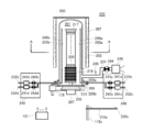
- FIG. 2 is a schematic configuration diagram of a vertical processing furnace of a substrate processing apparatus preferably used in an embodiment of the present invention, and is a diagram showing a processing furnace part in a cross-sectional view taken along line AA of FIG.
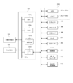
- the controller of the substrate processing apparatus used suitably by one Embodiment of this invention, and is a figure which shows the control system of a controller with a block diagram.
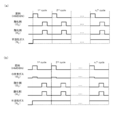
- (A) is a figure which shows the film-forming sequence of one Embodiment of this invention
- (b) is a figure which respectively shows the modification of the film-forming sequence of one Embodiment of this invention.
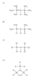
- (A)-(d) is a figure which shows the chemical structural formula of HMDSN, TMDSN, HCDSN, TSA in order. It is a figure which shows the evaluation result of the nitrogen concentration of the film
- the processing furnace 202 has a heater 207 as a heating mechanism (temperature adjustment unit).
- the heater 207 has a cylindrical shape and is vertically installed by being supported by a holding plate.
- the heater 207 also functions as an activation mechanism (excitation unit) that activates (excites) gas with heat.
- a reaction tube 203 is disposed inside the heater 207 concentrically with the heater 207.
- the reaction tube 203 is made of a heat-resistant material such as quartz (SiO 2 ) or silicon carbide (SiC), and is formed in a cylindrical shape with the upper end closed and the lower end opened.
- a manifold 209 is disposed below the reaction tube 203 concentrically with the reaction tube 203.
- the manifold 209 is made of a metal such as stainless steel (SUS), for example, and is formed in a cylindrical shape with an upper end and a lower end opened. The upper end portion of the manifold 209 is engaged with the lower end portion of the reaction tube 203 and is configured to support the reaction tube 203.
- An O-ring 220a as a seal member is provided between the manifold 209 and the reaction tube 203.
- the reaction tube 203 is installed vertically like the heater 207.
- the reaction vessel 203 and the manifold 209 mainly constitute a processing vessel (reaction vessel).
- a processing chamber 201 is formed in the cylindrical hollow portion of the processing container.
- the processing chamber 201 is configured to accommodate a plurality of wafers 200 as substrates.
- nozzles 249a and 249b are provided so as to penetrate the side wall of the manifold 209.
- Gas supply pipes 232a and 232b are connected to the nozzles 249a and 249b, respectively.
- the gas supply pipes 232a and 232b are provided with mass flow controllers (MFC) 241a and 241b as flow rate controllers (flow rate control units) and valves 243a and 243b as opening / closing valves, respectively, in order from the upstream side.
- MFC mass flow controllers
- Gas supply pipes 232c and 232d for supplying an inert gas are connected to the gas supply pipes 232a and 232b on the downstream side of the valves 243a and 243b, respectively.
- the gas supply pipes 232c and 232d are provided with MFCs 241c and 241d and valves 243c and 243d, respectively, in order from the upstream side.
- the nozzles 249 a and 249 b are arranged in an annular space in plan view between the inner wall of the reaction tube 203 and the wafer 200, along the upper portion from the lower portion of the inner wall of the reaction tube 203. Each is provided so as to rise upward in the stacking direction. That is, the nozzles 249a and 249b are respectively provided along the wafer arrangement area in the area horizontally surrounding the wafer arrangement area on the side of the wafer arrangement area where the wafers 200 are arranged. Gas supply holes 250a and 250b for supplying gas are provided on the side surfaces of the nozzles 249a and 249b, respectively.
- the gas supply holes 250 a and 250 b are opened so as to face the center of the reaction tube 203, and gas can be supplied toward the wafer 200.
- a plurality of gas supply holes 250a and 250b are provided from the lower part to the upper part of the reaction tube 203, each having the same opening area, and further provided at the same opening pitch.
- annular shape in a plan view defined by the inner wall of the side wall of the reaction tube 203 and the ends (peripheral portions) of the plurality of wafers 200 arranged in the reaction tube 203 is provided.
- Gas is conveyed through nozzles 249a and 249b arranged in a vertically long space, that is, in a cylindrical space.
- gas is first ejected into the reaction tube 203 from the gas supply holes 250a and 250b opened in the nozzles 249a and 249b, respectively, in the vicinity of the wafer 200.
- the main flow of gas in the reaction tube 203 is a direction parallel to the surface of the wafer 200, that is, a horizontal direction.
- the gas that flows on the surface of the wafer 200 flows toward the exhaust port, that is, the direction of the exhaust pipe 231 described later.
- the direction of the gas flow is appropriately specified depending on the position of the exhaust port, and is not limited to the vertical direction.
- the raw material gas is a raw material in a gaseous state, for example, a gas obtained by vaporizing a raw material that is in a liquid state under normal temperature and normal pressure, or a raw material that is in a gaseous state under normal temperature and normal pressure.
- the silazane compound is a compound having Si and N as a skeleton.
- the silazane-based source gas is a gas that acts not only as an Si source but also as an N source, or an N source and a C source.
- As the silazane-based source gas for example, hexamethyldisilazane ([(CH 3 ) 3 Si] 2 NH), abbreviation: HMDSN) gas can be used.
- HMDSN gas contains two Si—N bonds and six Si—C bonds in one molecule. Two Si bonds to one N (central element) in HMDSN. Three Cs are bonded to one Si included in the HMDSN.
- an oxygen (O) -containing gas is supplied as a reactant (reaction gas) into the processing chamber 201 via the MFC 241b, the valve 243b, and the nozzle 249b.
- the O-containing gas acts as an oxidizing agent (oxidizing gas), that is, an O source.
- oxygen (O 2 ) gas can be used as the O-containing gas.
- a hydrogen (H) -containing gas is supplied into the processing chamber 201 through the MFC 241a, the valve 243a, and the nozzle 249a as a reactant (reaction gas).
- the H-containing gas itself cannot oxidize, but reacts with the O-containing gas under specific conditions to generate oxidizing species such as atomic oxygen (O), thereby improving the efficiency of the oxidation treatment. It works to improve. Therefore, the H-containing gas can be considered to be included in the oxidizing agent (oxidizing gas) in the same manner as the O-containing gas.
- the H-containing gas for example, hydrogen (H 2 ) gas can be used.
- oxidant may include only an O-containing gas or may include both an O-containing gas and an H-containing gas.
- nitrogen (N 2 ) gas as an inert gas passes through the MFC 241c and 241d, the valves 243c and 243d, the gas supply pipes 232a and 232b, and the nozzles 249a and 249b, respectively. Supplied into 201.
- the gas supply pipe 232a, the MFC 241a, and the valve 243a constitute a raw material (raw material gas) supply system.
- a reactant (O-containing gas) supply system is mainly configured by the gas supply pipe 232b, the MFC 241b, and the valve 243b.
- a reactant (H-containing gas) supply system is mainly configured by the gas supply pipe 232a, the MFC 241a, and the valve 243a.
- the O-containing gas supply system functions as an oxidant supply system in a film forming process to be described later.
- the H-containing gas supply system may be included in the oxidant supply system.
- an inert gas supply system is mainly configured by the gas supply pipes 232c and 232d, the MFCs 241c and 241d, and the valves 243c and 243d.
- any or all of the various supply systems described above may be configured as an integrated supply system 248 in which valves 243a to 243d, MFCs 241a to 241d, and the like are integrated.
- the integrated supply system 248 is connected to each of the gas supply pipes 232a to 232d, and supplies various gases into the gas supply pipes 232a to 232d, that is, opens and closes the valves 243a to 243d and MFCs 241a to 241d.
- the flow rate adjusting operation and the like are configured to be controlled by a controller 121 described later.
- the integrated supply system 248 is configured as an integrated or split-type integrated unit, and can be attached to and detached from the gas supply pipes 232a to 232d in units of integrated units. Replacement, expansion, and the like can be performed in units of integrated units.
- the reaction tube 203 is provided with an exhaust pipe 231 for exhausting the atmosphere in the processing chamber 201.
- the exhaust pipe 231 is connected to a pressure sensor 245 as a pressure detector (pressure detection unit) for detecting the pressure in the processing chamber 201 and an APC (Auto Pressure Controller) valve 244 as a pressure regulator (pressure adjustment unit).
- a vacuum pump 246 as a vacuum exhaust device is connected.
- the APC valve 244 can perform vacuum evacuation and vacuum evacuation stop in the processing chamber 201 by opening and closing the valve with the vacuum pump 246 activated, and further, with the vacuum pump 246 activated,
- the pressure in the processing chamber 201 can be adjusted by adjusting the valve opening based on the pressure information detected by the pressure sensor 245.
- An exhaust system is mainly configured by the exhaust pipe 231, the APC valve 244, and the pressure sensor 245.
- the vacuum pump 246 may be included in the exhaust system.
- a seal cap 219 is provided as a furnace opening lid capable of airtightly closing the lower end opening of the manifold 209.
- the seal cap 219 is made of a metal such as SUS and is formed in a disk shape.
- an O-ring 220b is provided as a seal member that comes into contact with the lower end of the manifold 209.
- a rotation mechanism 267 for rotating a boat 217 described later is installed below the seal cap 219.
- a rotation shaft 255 of the rotation mechanism 267 passes through the seal cap 219 and is connected to the boat 217.
- the rotation mechanism 267 is configured to rotate the wafer 200 by rotating the boat 217.
- the seal cap 219 is configured to be raised and lowered in the vertical direction by a boat elevator 115 as an elevating mechanism installed outside the reaction tube 203.
- the boat elevator 115 is configured so that the boat 217 can be carried in and out of the processing chamber 201 by moving the seal cap 219 up and down.
- the boat elevator 115 is configured as a transfer device (transfer mechanism) that transfers the boat 217, that is, the wafers 200 into and out of the processing chamber 201.
- a shutter 219s is provided below the manifold 209 as a furnace port lid that can airtightly close the lower end opening of the manifold 209 while the seal cap 219 is lowered by the boat elevator 115.
- the shutter 219s is made of a metal such as SUS and is formed in a disk shape. On the upper surface of the shutter 219s, an O-ring 220c as a seal member that comes into contact with the lower end of the manifold 209 is provided.
- the opening / closing operation (elevating operation, rotating operation, etc.) of the shutter 219s is controlled by the shutter opening / closing mechanism 115s.
- the boat 217 as a substrate support is configured to support a plurality of, for example, 25 to 200, wafers 200 in a multi-stage manner by aligning them vertically in a horizontal posture and with their centers aligned. It is configured to arrange at intervals.
- the boat 217 is made of a heat-resistant material such as quartz or SiC. Under the boat 217, heat insulating plates 218 made of a heat-resistant material such as quartz or SiC are supported in multiple stages.
- a temperature sensor 263 is installed as a temperature detector. By adjusting the power supply to the heater 207 based on the temperature information detected by the temperature sensor 263, the temperature in the processing chamber 201 becomes a desired temperature distribution.
- the temperature sensor 263 is configured in an L shape similarly to the nozzles 249a and 249b, and is provided along the inner wall of the reaction tube 203.
- the controller 121 which is a control unit (control means), is configured as a computer having a CPU (Central Processing Unit) 121a, a RAM (Random Access Memory) 121b, a storage device 121c, and an I / O port 121d.
- the RAM 121b, the storage device 121c, and the I / O port 121d are configured to exchange data with the CPU 121a via the internal bus 121e.
- an input / output device 122 configured as a touch panel or the like is connected to the controller 121.
- the storage device 121c includes, for example, a flash memory, a HDD (Hard Disk Drive), and the like.
- a control program that controls the operation of the substrate processing apparatus, a process recipe that describes a film forming process procedure and conditions that will be described later, and the like are stored in a readable manner.
- the process recipe is a combination of processes so that a predetermined result can be obtained by causing the controller 121 to execute each procedure in a film forming process to be described later, and functions as a program.
- process recipes, control programs, and the like are collectively referred to simply as programs.
- the process recipe is also simply called a recipe.
- the RAM 121b is configured as a memory area (work area) in which programs, data, and the like read by the CPU 121a are temporarily stored.
- the I / O port 121d includes the above-described MFCs 241a to 241d, valves 243a to 243d, pressure sensor 245, APC valve 244, vacuum pump 246, temperature sensor 263, heater 207, rotation mechanism 267, boat elevator 115, shutter opening / closing mechanism 115s, etc. It is connected to the.
- the CPU 121a is configured to read out and execute a control program from the storage device 121c and to read a recipe from the storage device 121c in response to an operation command input from the input / output device 122 or the like.
- the CPU 121a adjusts the flow rate of various gases by the MFCs 241a to 241d, the opening / closing operation of the valves 243a to 243d, the opening / closing operation of the APC valve 244, and the pressure adjustment by the APC valve 244 based on the pressure sensor 245 so as to follow the contents of the read recipe.
- the controller 121 installs the above-mentioned program stored in an external storage device 123 (for example, a magnetic disk such as a hard disk, an optical disk such as a CD or a DVD, a magneto-optical disk such as an MO, or a semiconductor memory such as a USB memory) 123 on a computer.
- an external storage device 123 for example, a magnetic disk such as a hard disk, an optical disk such as a CD or a DVD, a magneto-optical disk such as an MO, or a semiconductor memory such as a USB memory
- the storage device 121c and the external storage device 123 are configured as computer-readable recording media. Hereinafter, these are collectively referred to simply as a recording medium.
- recording medium When the term “recording medium” is used in this specification, it may include only the storage device 121c alone, may include only the external storage device 123 alone, or may include both of them.
- the program may be provided to the computer using a communication means such as the Internet or a
- Step 1 of supplying an HMDSN gas as a raw material to a wafer 200 as a substrate, and (b) O 2 gas and H as oxidizing agents for the wafer 200.
- Step 2 in which two gases are simultaneously supplied (hereinafter, these gases to be supplied at the same time are also referred to as O 2 + H 2 gas), and a cycle in which the gases are supplied simultaneously, at least part of the Si—N bonds contained in the HMDSN gas
- a silicon oxynitride film as a film containing Si, N, and O is formed on the wafer 200 by performing a predetermined number of times (n 1 (n 1 is an integer equal to or greater than 1 )) under a condition of being held without being cut. (SiON film) is formed.
- the first layer including the Si—N bond is formed by supplying HMDSN under a condition in which at least a part of the Si—N bond included in the HMDSN is maintained without being broken.
- the first layer is unsaturated by supplying O 2 + H 2 gas under a condition that at least part of the Si—N bond contained in the first layer is maintained without being broken. Oxidized to form a second layer containing Si—N bonds and Si—O bonds.
- wafer when the term “wafer” is used, it means “wafer itself” or “a laminate (aggregate) of a wafer and a predetermined layer or film formed on the surface”. In other words, it may be called a wafer including a predetermined layer or film formed on the surface.
- wafer surface when the term “wafer surface” is used in this specification, it means “the surface of the wafer itself (exposed surface)” or “the surface of a predetermined layer or film formed on the wafer”. That is, it may mean “the outermost surface of the wafer as a laminated body”.
- the phrase “supplying a predetermined gas to the wafer” means “supplying a predetermined gas directly to the surface of the wafer itself” or “on the wafer. It may mean that a predetermined gas is supplied to the layer or film formed on the substrate, that is, the outermost surface of the wafer as a laminate. Further, in the present specification, the phrase “form a predetermined layer (or film) on the wafer” means “form a predetermined layer (or film) directly on the surface of the wafer itself”. In other cases, it may mean “to form a predetermined layer (or film) on a layer or film formed on the wafer, that is, on the outermost surface of the wafer as a laminate”.
- substrate is also synonymous with the term “wafer”.
- Vacuum exhaust (reduced pressure) is performed by the vacuum pump 246 so that the processing chamber 201, that is, the space where the wafer 200 exists, has a desired pressure (degree of vacuum).
- the pressure in the processing chamber 201 is measured by the pressure sensor 245, and the APC valve 244 is feedback-controlled based on the measured pressure information.
- the vacuum pump 246 maintains a state in which it is always operated until at least the processing on the wafer 200 is completed. Further, the wafer 200 in the processing chamber 201 is heated by the heater 207 so as to have a desired film formation temperature.
- the power supply to the heater 207 is feedback-controlled based on the temperature information detected by the temperature sensor 263 so that the inside of the processing chamber 201 has a desired temperature distribution. Heating of the processing chamber 201 by the heater 207 is continuously performed at least until the processing on the wafer 200 is completed. Further, the rotation of the boat 217 and the wafers 200 by the rotation mechanism 267 is started. The rotation of the boat 217 and the wafer 200 by the rotation mechanism 267 is continuously performed at least until the processing on the wafer 200 is completed.
- Step 1 HMDSN gas is supplied to the wafer 200 in the processing chamber 201.
- valve 243a is opened and the HMDSN gas is allowed to flow into the gas supply pipe 232a.
- the flow rate of the HMDSN gas is adjusted by the MFC 241a, supplied into the processing chamber 201 via the nozzle 249a, and exhausted from the exhaust pipe 231.
- the HMDSN gas is supplied to the wafer 200.
- the valve 243c is opened and N 2 gas is allowed to flow into the gas supply pipe 232c.
- the flow rate of the N 2 gas is adjusted by the MFC 241c, supplied into the processing chamber 201 through the gas supply pipe 232a and the nozzle 249a, and exhausted from the exhaust pipe 231.
- the valve 243d is opened and N 2 gas is allowed to flow into the gas supply pipe 232d.
- the N 2 gas is supplied into the processing chamber 201 through the gas supply pipe 232b and the nozzle 249b, and is exhausted from the exhaust pipe 231.
- the pressure (film formation pressure) in the processing chamber 201 is set to a predetermined pressure within a range of, for example, 0.1 to 20 Torr (13.3 to 2666 Pa), preferably 1 to 10 Torr (133 to 1333 Pa).
- the temperature (film formation temperature) of the wafer 200 is set to a predetermined temperature in the range of 450 to 1000 ° C., preferably 750 to 900 ° C., for example.
- the supply flow rate of the HMDSN gas is set to a predetermined flow rate in the range of, for example, 1 to 2000 sccm, preferably 10 to 1000 sccm.
- the supply time of the HMDSN gas is set to, for example, a predetermined time within a range of 1 to 100 seconds, preferably 1 to 50 seconds.
- the supply flow rate of N 2 gas supplied from each gas supply pipe is set to a predetermined flow rate in the range of, for example, 100 to 10,000 sccm. Note that the N 2 gas may not be supplied during the supply period of the HMDSN gas.
- the film forming pressure is less than 0.1 Torr (or the film forming temperature is less than 450 ° C.), it is difficult to form the SiON film on the wafer 200, and a practical film forming rate may not be obtained.
- the deposition pressure is set to 0.1 Torr or higher (or the deposition temperature to 450 ° C. or higher), it becomes possible to increase the deposition rate of the SiON film to a practical level.
- the pressure in the processing chamber 201 to 1 Torr or more (or the film formation temperature to 750 ° C. or more), the film formation rate of the SiON film can be further increased.
- the film forming pressure exceeds 20 Torr (or the film forming temperature exceeds 1000 ° C.)
- an excessive gas phase reaction occurs, so that the film thickness uniformity of the SiON film formed on the wafer 200 tends to deteriorate.
- a large amount of particles may be generated in the processing chamber 201, which may deteriorate the quality of the film forming process.
- the flatness of the surface of the SiON film that is, the surface roughness may be deteriorated.
- the Si—N bond included in the HMDSN is cut, and it may be difficult to properly include the Si—N bond in the SiON film.
- the hydrogen fluoride (HF) of the SiON film may be obtained. Etching resistance to the above may decrease.
- the film formation pressure By setting the film formation pressure to 20 Torr or less (or the film formation temperature to 1000 ° C. or less), an appropriate gas phase reaction can be generated, thereby improving the film thickness uniformity and surface roughness of the SiON film, It is possible to suppress the generation of particles. In addition, it becomes possible to retain at least a part of the Si—N bond contained in the HMDSN without breaking, and it is possible to improve the etching resistance of the SiON film by adding the Si—N bond in the film. . By setting the film forming pressure to 10 Torr or lower (or the film forming temperature to 900 ° C. or lower), the film thickness uniformity and surface roughness of the SiON film are reliably improved, and the generation of particles in the processing chamber 201 is ensured. Can be suppressed.
- surface roughness means a difference in film height in the wafer plane, and is synonymous with surface roughness.
- An improvement in surface roughness means that this height difference is reduced and the surface becomes smooth.
- the deterioration of the surface roughness means that the height difference becomes large and the surface becomes rough.
- the film formation pressure is set to a predetermined pressure in the range of 0.1 to 20 Torr, preferably 1 to 10 Torr, and the film formation temperature is 450 to 1000 ° C., preferably 750 to 900. It is good to set it as the predetermined temperature within the range of ° C.
- the processing conditions (pressure conditions and temperature conditions) described here are such that when the HMDSN gas is present alone in the processing chamber 201, the HMDSN is thermally decomposed (self-decomposing) and the Si—N bonds contained in the HMDSN. It includes a condition that at least a part and at least a part of the Si—C bond are maintained without being broken.
- the first layer is formed on the outermost surface of the wafer 200, for example, from less than one atomic layer to several atomic layers (from less than one molecular layer).
- a Si-containing layer containing N and C having a thickness of several molecular layers is formed.
- the Si-containing layer containing N and C may be an Si layer containing N and C, an adsorption layer of HMDSN, or both of them.
- the Si-containing layer containing N and C is also a layer containing Si—N bonds and Si—C bonds, respectively.
- the Si layer containing N and C is a generic name including a continuous layer composed of Si and containing N and C, a discontinuous layer, and an Si thin film containing N and C formed by overlapping these layers. .
- Si constituting the Si layer containing N and C includes not only completely broken bonds with N and C, but also those completely broken with N and C.
- the adsorption layer of HMDSN includes a discontinuous adsorption layer as well as a continuous adsorption layer composed of HMDSN molecules.
- HMDSN molecules constituting the HMDSN adsorption layer include those in which the bond between Si and N is partially broken and those in which the bond between Si and C is partially broken. That is, the HMDSN adsorption layer may be a HMDSN physical adsorption layer, a HMDSN chemical adsorption layer, or may include both of them.
- the layer having a thickness less than one atomic layer means a discontinuously formed atomic layer (molecular layer), and a layer having a thickness of one atomic layer (molecular layer).
- the Si-containing layer containing N and C can include both an Si layer containing N and C and an adsorption layer of HMDSN.
- the Si-containing layer containing N and C is expressed using expressions such as “one atomic layer” and “several atomic layer”, and “atomic layer” may be used synonymously with “molecular layer”. is there.
- Si is deposited on the wafer 200 to form a Si layer containing N and C.
- the HMDSN adsorbing layer is formed by adsorbing the HMDSN on the wafer 200. It is preferable to form a Si layer containing N and C on the wafer 200 in that the deposition rate can be increased, rather than forming an HMDSN adsorption layer on the wafer 200.
- the Si-containing layer containing N and C is also simply referred to as a Si-containing layer for convenience.
- the thickness of the first layer exceeds several atomic layers, the modification effect in Step 2 described later does not reach the entire first layer.
- the minimum thickness of the first layer is less than one atomic layer. Therefore, it is preferable that the thickness of the first layer be less than one atomic layer to several atomic layers.
- the action of the reforming reaction in Step 2 described later can be relatively enhanced.
- the time required for the reforming reaction can be shortened.
- the time required for forming the first layer in step 1 can also be shortened. As a result, the processing time per cycle can be shortened, and the total processing time can be shortened. That is, the film forming rate can be increased.
- the controllability of the film thickness uniformity can be improved by setting the thickness of the first layer to 1 atomic layer or less.
- the valve 243a is closed and the supply of the HMDSN gas is stopped.
- the APC valve 244 is kept open, the processing chamber 201 is evacuated by the vacuum pump 246, and the HMDSN gas or reaction by-product remaining in the processing chamber 201 is contributed to the formation of the unreacted or first layer.
- Objects are removed from the processing chamber 201.
- the valves 243c and 243d remain open, and the supply of N 2 gas into the processing chamber 201 is maintained. N 2 gas acts as a purge gas.
- tetramethyldisilazane [H (CH 3 ) 2 Si] 2 NH), abbreviation: TMDSN
- hexachlorodisilazane (Cl 3 Si) 2 NH, abbreviation: HCDSN) gas
- Silazane compounds such as trisilylamine (N (SiH 3 ) 3 , abbreviation: TSA) gas can be used.
- the TMDSN gas contains two Si—N bonds and four Si—C bonds in one molecule, and like the HMDSN gas, the Si source, It is a gas that acts as an N source and a C source.
- One N (central element) in TMDSN is bonded with two Si similarly to that in HMDSN, and this allows Si—N bonds to be included in the first layer under the above-described processing conditions. It becomes easy.
- Two Cs are bonded to one Si included in TMDSN. Since the number of Si—C bonds contained in TMDSN (four) is less than the number of Si—C bonds contained in HMDSN (six), the action as a C source in TMDSN gas is that of HMDSN gas. Tend to be weaker.
- the HCDSN gas contains two Si—N bonds in one molecule and does not contain an Si—C bond, and thus acts as an Si source and an N source. It is a gas that does not act as a C source.
- One N (central element) in HCDSN is bonded with two Si similarly to that in HMDSN. This allows Si—N bonds to be included in the first layer under the processing conditions described above. It becomes easy.
- the TSA gas contains three Si—N bonds in one molecule and does not contain Si—C bonds. It is a gas that does not act as a C source. Three Si bonds to one N (central element) in TSA.
- TSA gas is used as the source gas, a larger amount of Si—N bonds are formed in the first layer under the above-described processing conditions than when HMDSN gas, TMDSN gas, and HCDSN gas are used as the source gas. It becomes easy to include.
- silazane compounds are silane compounds such as dichlorosilane (SiH 2 Cl 2 ) gas, hexachlorodisilane (Si 2 Cl 6 , abbreviation: HCDS) gas, tetrachlorosilane (SiCl 4 ) gas, tetrafluorosilane (SiF 4 ).
- a halosilane compound such as tetrabromosilane (SiBr 4 ) gas, trisdimethylaminosilane (Si [N (CH 3 ) 2 ] 3 H, abbreviation: 3DMAS) gas, bistertiary butylaminosilane (SiH 2 [NH (C 4 H 9)] 2, abbreviated: BTBAS) gas, diisopropylaminosilane (SiH 3 N [CH (CH 3) 2] 2, abbreviated: DIPAS) and aminosilane compound such as a gas, monosilane (SiH 4) gas, disilane ( Si 2 H 6) gas, trisilane (S 3 H 8) as compared to the silicon hydride compounds, such as gas, thermal decomposition temperature is high (hardly self-decomposition) tend.
- thermal decomposition temperature is high (hardly self-decomposition) tend.
- the inert gas for example, a rare gas such as Ar gas, He gas, Ne gas, or Xe gas can be used in addition to N 2 gas.
- a rare gas such as Ar gas, He gas, Ne gas, or Xe gas can be used in addition to N 2 gas.
- Step 2 After step 1 is completed, O 2 gas and H 2 gas are separately supplied into the processing chamber 201, and these gases are mixed and reacted in the processing chamber 201. Step 2 includes a period in which O 2 gas and H 2 gas are supplied simultaneously.
- valves 243b and 243a are opened, and O 2 gas and H 2 gas are allowed to flow through the gas supply pipes 232b and 232a, respectively.
- the opening / closing control of the valves 243c, 243d is performed in the same procedure as the opening / closing control of the 243c, 243d in Step 1.
- the flow rates of the O 2 gas and H 2 gas flowing through the gas supply pipes 232b and 232a are adjusted by the MFCs 241b and 241a, respectively, and are supplied into the processing chamber 201 through the nozzles 249b and 249a. O 2 gas and H 2 gas are mixed and reacted for the first time in the processing chamber 201, and then exhausted from the exhaust pipe 231.
- the pressure (deposition pressure) in the processing chamber 201 is set to a predetermined value within a range of, for example, 0.1 to 10 Torr (13.3 to 1333 Pa), preferably 0.1 to 3 Torr (13.3 to 399 Pa). Pressure.
- the supply flow rates of the O 2 gas and the H 2 gas are set to predetermined flow rates in the range of, for example, 100 to 10,000 sccm.
- the supply time of O 2 gas and H 2 gas is, for example, a predetermined time in the range of 1 to 100 seconds, preferably 1 to 50 seconds.
- Other processing conditions are the same as the processing conditions in step 1. Note that as in step 1, the N 2 gas may not be supplied during the supply period of the O 2 + H 2 gas.
- the O 2 gas and H 2 gas is thermally activated in a non-plasma in the heated reduced pressure atmosphere (excitation) And reacts to produce moisture (H 2 O) -free oxidizing species containing oxygen, such as atomic oxygen (O).
- an oxidation treatment is performed on the first layer formed on the wafer 200 in Step 1 mainly by this oxidation species.
- the oxidizing power can be greatly improved as compared with the case of supplying O 2 gas alone or the case of supplying water vapor (H 2 O gas). That is, by adding H 2 gas to O 2 gas in a reduced pressure atmosphere, a significant effect of improving the oxidizing power can be obtained as compared with the case of supplying O 2 gas alone or the case of supplying H 2 O gas.
- the energy of the oxidized species generated by the above method is higher than the bond energy of Si—C bond, Si—H bond, etc. contained in the first layer, the energy of this oxidized species is given to the first layer.
- most of the Si—C bonds and Si—H bonds contained in the first layer can be cut.
- C, H, etc., from which the bond with Si is cut off will be removed from the first layer.
- most of C and H contained in the first layer can be desorbed, and C and H in the first layer can be reduced to the impurity level.
- the remaining Si bonds due to the disconnection with C, H, etc. are linked to O contained in the oxidized species, thereby forming a Si—O bond. That is, O is taken into the first layer in the form of Si—O bonds.
- the energy possessed by the above-mentioned oxidized species is higher than the bond energy such as Si—N bonds contained in the first layer, but at least under the above-mentioned conditions, at least the Si—N bonds contained in the first layer. A part can be held without cutting. That is, under the above-described conditions, the oxidation treatment of the first layer with the oxidizing species can be made unsaturated (unsaturated oxidation) with respect to at least the Si—N bond contained in the first layer.
- the above-described processing conditions can be said to be conditions for cutting the Si—C bonds contained in the first layer and holding at least a part of the Si—N bonds contained in the first layer without breaking.
- the treatment conditions for example, the supply flow rate of the oxidant, the partial pressure of the oxidant, the supply time of the oxidant, the kind of the oxidant, etc. are appropriately adjusted, It is effective to make a selection. That is, the supply flow rate and partial pressure of the oxidant are set to be small within the above range, the supply time of the oxidant is set to be short within the above range, or a substance having a relatively weak oxidizing power is used as the oxidant. By doing so, the above-described oxidation treatment can be surely unsaturated. According to the earnest studies by the inventors, among the above four treatment conditions, two of the oxidizing agent partial pressure and the oxidizing agent supply time are particularly effective for making the oxidation treatment unsaturated. I know that there is.
- the oxidation treatment in Step 2 unsaturated it is also effective to increase the state of the first layer to be treated, for example, the amount of Si—N bonds contained in the first layer.
- the amount of Si—N bonds contained in the first layer can be increased, thereby ensuring that the oxidation treatment is unsaturated. It becomes possible.
- the amount of Si—N bonds contained in the first layer can be increased.
- the oxidation treatment can be surely unsaturated.
- the above-described oxidation treatment can be surely unsaturated, and at least a part of the Si—N bonds contained in the first layer can be reliably left.
- the state of the first layer may be changed by adjusting the processing conditions in Step 1 while keeping the processing conditions of the oxidation processing in Step 2 constant. Further, the processing conditions of the oxidation treatment in step 2 may be changed while the processing conditions in step 1 are kept constant and the state of the first layer is maintained. Further, both of the processing conditions in steps 1 and 2 may be adjusted.
- the first layer is changed (modified) into a second layer containing Si, O, and N, that is, a C-free SiON layer.
- the second layer is a layer containing Si—N bonds, that is, a layer containing N in the form of Si—N bonds.
- valves 243b and 243a are closed, and the supply of O 2 gas and H 2 gas is stopped. Then, the unreacted or remaining O 2 gas, H 2 gas, and reaction by-products remaining in the processing chamber 201 are excluded from the processing chamber 201 by the same processing procedure and processing conditions as in Step 1. To do.
- oxygen (O 2 ) gas in addition to O 2 + H 2 gas, oxygen (O 2 ) gas, water vapor (H 2 O), ozone (O 3 ) gas, plasma-excited O 2 (O 2 * ) gas, atomic oxygen (O), oxygen radicals (O * ), hydroxyl radicals (OH * ), and the like can be used.
- deuterium (D 2) in place of the H 2 gas may be a gas or the like.
- the inert gas in addition to N 2 gas, the above-mentioned various rare gases can be used.
- a SiON film having a predetermined thickness can be formed on the wafer 200.
- the above cycle is preferably repeated multiple times. That is, the thickness of the second layer formed when the above cycle is performed once is made smaller than the desired thickness, and the thickness of the SiON film formed by stacking the second layers is the desired thickness.
- the above cycle is preferably repeated a plurality of times until the thickness is reached.
- N 2 gas is supplied from the gas supply pipes 232c and 232d into the processing chamber 201 and exhausted from the exhaust pipe 231.
- N 2 gas acts as a purge gas.
- the inside of the processing chamber 201 is purged, and the gas and reaction byproducts remaining in the processing chamber 201 are removed from the processing chamber 201 (after purge).
- the atmosphere in the processing chamber 201 is replaced with an inert gas (inert gas replacement), and the pressure in the processing chamber 201 is returned to normal pressure (return to atmospheric pressure).
- the film formed on the wafer 200 can be a film having high oxidation resistance (ashing resistance).
- ashing resistance oxidation resistance
- N that is incorporated into the film in the form of Si—N bonds acts as a protective element that suppresses oxidation of the film
- N that is incorporated into the film in the form of N—H bonds. May induce membrane oxidation.
- the film formed according to the present embodiment includes N in the form of Si—N bonds, a film formed using NH 3 gas as the N source (a film including N in the form of N—H bonds) In comparison, even if the N concentration of the film is similar, high ashing resistance is exhibited.
- the film formation temperature is less than 450 ° C., for example, within the range of 250 to 400 ° C. It becomes possible to improve the etching resistance and insulation performance of the SiON film, extend the service life, and reduce the interface electron trap density that affects the response speed of the transistor. In particular, by setting the film forming temperature within the range of 700 to 1000 ° C., it is possible to further improve the film characteristics of the above-described SiON film.
- a nitrogen oxide-based gas having a relatively weak oxidizing power such as nitrous oxide (N 2 O) gas, nitrogen monoxide (NO) gas, nitrogen dioxide (NO 2 ) gas, for example, N 2 O gas may be used to further increase the degree of unsaturation in the oxidation treatment of the first layer. That is, when the cycle is performed a predetermined number of times (n 2 times (n 2 is an integer of 1 or more)), in step 2, at least part of the Si—N bonds and at least part of the Si—C bonds contained in the first layer The oxidant may be supplied under the condition that the first layer is maintained without being cut, and the degree of unsaturation of the oxidation treatment on the first layer may be further increased.
- N 2 O nitrous oxide
- NO nitrogen monoxide
- NO 2 nitrogen dioxide
- the first layer is changed (modified) into a second layer containing Si, O, C, and N, that is, a silicon oxycarbonitride layer (SiOCN layer), on the wafer 200.
- a silicon oxycarbonitride film SiOCN film
- This film is a film including a Si—N bond, a Si—C bond, and a Si—O bond.
- the film forming sequence of this modification is shown below using the symbol [b].
- the processing conditions at this time can be the same processing conditions as the film forming sequence shown in FIG.
- the oxidation treatment of the first layer with the oxidizing species can be made unsaturated (unsaturated oxidation) with respect to at least the Si—N bond and the Si—C bond contained in the first layer.
- the same effect as the film forming sequence shown in 4 (a) can be obtained.
- by including C in the film it is possible to form a film having higher etching resistance than a C-free SiO film or a C-free SiON film.
- a quaternary film can be formed without separately supplying four sources of Si source, O source, C source, and N source, as shown in FIG. Similar to the film forming sequence, the productivity of the film forming process can be improved and the cost of the apparatus can be reduced.
- the oxidizing power of the oxidizing agent supplied in step 2 needs to be lower than that in the film forming sequence shown in FIG.
- a substance containing O and N for example, a nitrogen oxide gas having a relatively weak oxidizing power such as N 2 O gas, NO gas, NO 2 gas, etc.
- the degree of unsaturation in the oxidation process in step 2 And the Si—N bonds and Si—C bonds contained in the first layer can be maintained as described above.
- the supply flow rate or partial pressure of the oxidant is set smaller than that in the film forming sequence shown in FIG.
- the degree of unsaturation in the oxidation process in step 2 is increased, and Si—N bonds and Si contained in the first layer are increased. It becomes possible to hold the -C bond as described above.
- the oxidation treatment of the first layer may be saturated by setting a large supply flow rate and partial pressure of the oxidizer or setting a long supply time of the oxidizer. That is, when the cycle is performed a predetermined number of times (n 3 times (n 3 is an integer of 1 or more)), in step 2, the Si—N bond and the Si—C bond contained in the first layer are respectively cut under the conditions.
- An oxidizing agent may be supplied to saturate and oxidize the first layer.
- the first layer is changed (modified) into a second layer containing Si and O, that is, a silicon oxide layer (SiO layer), and a silicon oxide film (on the wafer 200) SiO film) is formed.
- This film includes a Si—O bond and does not include a Si—N bond and a Si—C bond.
- the film forming sequence of this modification is shown below using the symbol [c].
- the SiO film is formed (deposited) on the wafer 200 instead of oxidizing the surface of the wafer 200, the diffusion of O to the surface of the wafer 200 can be suppressed.
- the step coverage of the film, the film thickness controllability, and the in-plane film thickness are uniform. It becomes possible to improve property.
- the film forming temperature is set to a predetermined temperature within the range of 450 to 1000 ° C., so that the etching resistance and insulating performance of the film are improved. It is possible to improve, extend the service life, and reduce the interface electron trap density.
- an oxidizing agent such as O 2 + H 2 gas, O * , OH * , O 3 gas, H 2 O gas, or O 2 gas is used as an oxidizing agent. It is preferable to use a relatively strong O-containing gas, that is, an N-free O-containing gas.
- Modification 3 For example, by selecting at least any two of the film forming sequences indicated by the symbols [a] to [c] and alternately performing them a predetermined number of times (n 4 times (n 4 is an integer of 1 or more)), You may make it form the laminated film by which the film from which at least any one of C density
- the outermost surface of the laminated film may be formed as a SiON film by performing a film forming sequence indicated by symbol [a] at the end.
- the outermost surface of the stacked film may be formed as a SiOCN film by performing a film forming sequence indicated by a symbol [b] at the end.
- the outermost surface of the laminated film may be formed as a SiO film by performing a film forming sequence indicated by a symbol [c] at the end. ([A] ⁇ [c]) ⁇ n 4 ([B] ⁇ [c]) ⁇ n 4 ([A] ⁇ [b] ⁇ [c]) ⁇ n 4 ([B] ⁇ [a] ⁇ [c]) ⁇ n 4
- the lowermost surface of the laminated film may be formed as a SiON film by first performing the film forming sequence indicated by symbol [a], or the lowermost surface of the laminated film by performing the film forming sequence indicated by symbol [b] first.
- the finally formed laminated film can be a film having a uniform characteristic in the thickness direction, that is, a nanolaminate film having an integral inseparable characteristic as a whole.
- a nanolaminate film for example, a film having the characteristics of each film in a well-balanced manner can be formed.
- the film thickness of each film constituting the laminated film can be set as described above.
- the thickness can be within the range of.
- the thickness of the laminated film is adjusted by adjusting at least one of the number of cycles (n 1 to n 3 ) in the film forming sequence indicated by symbols [a] to [c].
- a gradient (gradation) of at least one of C density and N density may be provided in the vertical direction. In this case, for example, a gradation in which the N concentration or the C concentration gradually increases from the bottom surface to the top surface in the thickness direction of the laminated film, or a gradation in which the N concentration or the C concentration gradually decreases is added. Is possible.
- step 1 As shown in FIG. 4B and the film forming sequence shown below, in step 1, an HMDSN gas as a raw material and, for example, an O 2 gas as an O-containing gas are supplied to the wafer 200 simultaneously. May be.
- the supply of O 2 gas in step 1 is performed from the gas supply pipe 232b.
- the supply amount of O 2 gas in Step 1 per cycle (Q 1), the supply amount of O 2 gas in Step 2 per cycle (Q 2) is from less (Q 1 ⁇ Q 2).
- O 2 gas supply flow rate (F 1) in step 1 is smaller than the supply flow rate of O 2 gas (F 2) in step 2 (F 1 ⁇ F 2 ), for example, 1/20 to 1/2 of the F 2, preferably 1/10 or more than 1/5.
- F 1 can be, for example, in the range of 1 to 1000 sccm, preferably 2 to 400 sccm.
- F 1 When F 1 is less than 1/20 of F 2 (or less than 1 sccm), may O 2 Si migration that will be described later by gas (mobile) inhibiting effect can not be obtained in step 1, it is formed on the wafer 200
- the surface roughness of the SiON film tends to deteriorate.
- F 1 By setting F 1 to be 1/20 or more (or 1 sccm or more) of F 2 , a migration suppressing effect can be obtained, and the surface roughness of the SiON film can be improved.
- F 1 By setting F 1 to be 1/10 or more of F 2 (or 2 sccm or more), a migration suppressing effect can be obtained with certainty, and the surface roughness of the SiON film can be improved with certainty.
- Step 1 If F 1 exceeds 1/2 of F 2 (or exceeds 1000 sccm), an excessive gas phase reaction occurs in Step 1, so that the film thickness uniformity of the SiON film formed on the wafer 200 is likely to deteriorate. There is a case.
- F 1 By setting F 1 to be 1 ⁇ 2 or less (or 1000 sccm or less) of F 2 , an appropriate gas phase reaction can be generated in Step 1, thereby making it possible to improve the film thickness uniformity of the SiON film.
- F 1 to 1/5 or less of F 2 (or 400 sccm or less) the gas phase reaction can be appropriately suppressed in Step 1, and the film thickness uniformity of the SiON film can be reliably improved. It becomes.
- Step 1 by simultaneously supplying the raw material and the O-containing gas to the wafer 200, at least a part of this Si is simultaneously or simultaneously with the adsorption of Si onto the wafer 200. It can be oxidized to change to oxide (SiO x ). Si adsorbed on the wafer 200 becomes difficult to migrate due to oxidation. That is, migration of Si atoms adsorbed on the wafer 200 is hindered by O atoms bonded to Si atoms. More specifically, migration of Si atoms is blocked by O atoms adjacent to Si atoms adsorbed on wafer 200. Thereby, aggregation of Si adsorbed on the wafer 200 can be suppressed.
- oxide Si adsorbed on the wafer 200
- the interface roughness between the base and the SiON film and the surface roughness of the SiON film can be improved.
- the relationship of Q 1 ⁇ Q 2 is maintained as in this modification, even if the O-containing gas is supplied simultaneously with the raw material in Step 1, the oxidizing power can be appropriately suppressed, It is possible to include Si—N bonds and Si—C bonds in one layer. As a result, also in this modification, it is possible to obtain the same effect as the film forming sequence shown in FIG.
- the supply time (T 1 ) of the O-containing gas (O 2 gas) per cycle is changed to F 1 ⁇ F 2 without oxidizing F 1 ⁇ F 2.
- agent (O 2) supply time (T 2) may be shorter than (T 1 ⁇ T 2).
- F 1 ⁇ F 2 may be set, and T 1 ⁇ T 2 may be set.
- the oxidizing power in step 1 can be appropriately suppressed, and the Si—N bond or Si—C bond can be included in the first layer, as shown in FIG. The same effect as the film forming sequence can be obtained.
- the oxidizing agent supplied in step 2 and the O-containing gas supplied in step 1 may have the same molecular structure (chemical structure) as shown in FIG. May have different molecular structures. That is, the oxidizing material supplied in step 2 and the O-containing gas supplied in step 1 may be the same material or different materials. However, if the O-containing gas supplied in Step 1 is a substance having a lower oxidizing power than the oxidant supplied in Step 2, Si—N bonds or Si—C bonds may be included in the first layer. It is preferable in terms of ease. Examples of the substance having an oxidizing power smaller than that of O 2 + H 2 gas include O 2 * gas, O 3 gas, H 2 O gas, O 2 gas, N 2 O gas, NO gas, and NO 2 gas. .
- the Si—N bond or the Si—C bond is surely included in the first layer. It is preferable at the point which becomes possible.
- a nitrogen oxide-based gas is used as the O-containing gas used in Step 1, it is possible to include Si—N bonds or Si—C bonds in the first layer even if Q 1 ⁇ Q 2 .
- the effect of improving the surface roughness by simultaneously supplying the raw material and the O-containing gas in Step 1 is not limited to the case where the film forming temperature is within the range of 450 to 1000 ° C., but is less than 450 ° C., for example, 250 to 400 Even when the temperature is within the range of ° C., it can be obtained in the same manner.
- the migration of Si tends to become more active as the film formation temperature becomes higher, and becomes prominent when the film formation temperature falls within a range of 700 to 1000 ° C., for example. Therefore, the technical significance of simultaneously supplying the raw material and the O-containing gas in Step 1 is that the migration of Si contained in the HMDSN gas is remarkable when the film formation temperature is supplied to the wafer 200 alone. It becomes particularly large when the above-mentioned temperature is generated (temperature in the range of 700 to 1000 ° C.).
- the present invention is not limited to such an embodiment, and the supply order of the raw material and the oxidizing agent may be reversed. That is, the raw material may be supplied after the oxidizing agent is supplied. By changing the supply order, the film quality and composition ratio of the formed film can be changed.
- the present invention is not limited to such an embodiment. That is, the present invention can be suitably applied to the case where a film containing a metal element such as germanium (Ge) or boron (B) as a main element in addition to Si is formed on a substrate.
- the present invention also provides titanium (Ti), zirconium (Zr), hafnium (Hf), niobium (Nb), tantalum (Ta), molybdenum (Mo), tungsten (W), yttrium (Y), and lanthanum (La).
- the present invention can also be suitably applied to the case where a film containing a metal element such as strontium (Sr) or aluminum (Al) as a main element is formed on a substrate.
- the recipe used for the substrate processing is preferably prepared individually according to the processing content and stored in the storage device 121c via the telecommunication line or the external storage device 123. And when starting a board
- the above-described recipe is not limited to a case of newly creating, but may be prepared by changing an existing recipe that has already been installed in the substrate processing apparatus, for example.
- the changed recipe may be installed in the substrate processing apparatus via an electric communication line or a recording medium on which the recipe is recorded.
- an existing recipe already installed in the substrate processing apparatus may be directly changed by operating the input / output device 122 provided in the existing substrate processing apparatus.
- a film is formed using a batch-type substrate processing apparatus that processes a plurality of substrates at one time.
- the present invention is not limited to the above-described embodiment, and can be suitably applied to a case where a film is formed using, for example, a single-wafer type substrate processing apparatus that processes one or several substrates at a time.
- a film is formed using a substrate processing apparatus having a hot wall type processing furnace.
- the present invention is not limited to the above-described embodiment, and can be suitably applied to a case where a film is formed using a substrate processing apparatus having a cold wall type processing furnace.
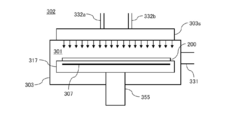
- the present invention can be suitably applied also when a film is formed using a substrate processing apparatus including the processing furnace 302 shown in FIG.
- the processing furnace 302 includes a processing container 303 that forms the processing chamber 301, a shower head 303s as a gas supply unit that supplies gas into the processing chamber 301 in a shower shape, and one or several wafers 200 in a horizontal posture.
- a support base 317 for supporting, a rotating shaft 355 for supporting the support base 317 from below, and a heater 307 provided on the support base 317 are provided.
- Gas supply ports 332a and 332b are connected to the inlet of the shower head 303s.
- the gas supply port 332a is connected to a supply system similar to the raw material supply system and the H-containing gas supply system of the above-described embodiment.
- a supply system similar to the O-containing gas supply system of the above-described embodiment is connected to the gas supply port 332b.
- a gas dispersion plate is provided at the outlet of the shower head 303s.
- the shower head 303 s is provided at a position facing (facing) the surface of the wafer 200 carried into the processing chamber 301.
- the processing vessel 303 is provided with an exhaust port 331 for exhausting the inside of the processing chamber 301.
- An exhaust system similar to the exhaust system of the above-described embodiment is connected to the exhaust port 331.
- the processing furnace 402 includes a processing container 403 that forms a processing chamber 401, a support base 417 that supports one or several wafers 200 in a horizontal position, a rotating shaft 455 that supports the support base 417 from below, and a processing container.
- a lamp heater 407 that irradiates light toward the wafer 200 in the 403 and a quartz window 403w that transmits light from the lamp heater 407 are provided.
- Gas supply ports 432 a and 432 b are connected to the processing container 403.
- the gas supply port 432a is connected to a supply system similar to the raw material supply system and the H-containing gas supply system of the above-described embodiment.
- a supply system similar to the O-containing gas supply system of the above-described embodiment is connected to the gas supply port 432b.
- the gas supply ports 432a and 432b are provided on the sides of the end of the wafer 200 loaded into the processing chamber 401, respectively.
- the processing container 403 is provided with an exhaust port 431 for exhausting the inside of the processing chamber 401.
- An exhaust system similar to the exhaust system of the above-described embodiment is connected to the exhaust port 431.
- the film forming process can be performed with the same processing procedure and processing conditions as in the above-described embodiment and modification, and the same effect as in the above-described embodiment and modification can be obtained. It is done.
- processing procedure and processing conditions at this time can be the same as the processing procedure and processing conditions of the above-described embodiment, for example.
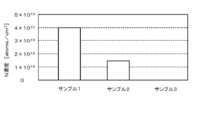
- the oxidant supply time in step 2 is a predetermined time within a range of 5 to 10 seconds when the sample 1 is manufactured, and a predetermined time within a range of 12 to 20 seconds when the sample 2 is manufactured.
- each was set to a predetermined time within the range of 50 to 80 seconds.
- the other processing conditions are those within the processing condition range described in the above embodiment, and are set so as to be common conditions for the samples 1 to 3.
- the N concentration of each film in samples 1 to 3 was measured.
- the result is shown in FIG.
- the film of Sample 1 contains N at a high concentration in the film.
- membrane of sample 2 contains N in a film
- the film of Sample 3 contains almost no N in the film.
- the N concentration of the film formed on the wafer can be controlled over a wide range by adjusting the supply time of the oxidizing agent in Step 2. That is, it can be seen that if the supply time of the oxidizing agent is lengthened, the N concentration of the film can be lowered and the composition of the film can be made closer to the SiO film. It can also be seen that when the supply time of the oxidizing agent is shortened, the composition of the film can be made closer to that of the SiON film without reducing the N concentration of the film. Note that the inventors can control the N concentration of the film over a wide range not only by supplying the oxidizing agent but also by appropriately adjusting and selecting the supply flow rate, partial pressure, and type of the oxidizing agent. It is also confirmed. The inventors have also confirmed that, among these factors, two of the partial pressure of the oxidant and the supply time are particularly effective for controlling the N concentration.
- Controller 200 wafer (substrate) 201 processing chamber 202 processing furnace 203 reaction pipe 207 heater 231 exhaust pipe 232a to 232d gas supply pipe
Landscapes
- Chemical & Material Sciences (AREA)
- General Chemical & Material Sciences (AREA)
- Chemical Kinetics & Catalysis (AREA)
- Engineering & Computer Science (AREA)
- Materials Engineering (AREA)
- Mechanical Engineering (AREA)
- Metallurgy (AREA)
- Organic Chemistry (AREA)
- Inorganic Chemistry (AREA)
- Chemical Vapour Deposition (AREA)
- Formation Of Insulating Films (AREA)
Abstract
Selon la présente invention, un cycle de mise en œuvre non simultanée d'une étape (a) d'injection, sur un substrat, d'une matière première incluant au moins deux liaisons chimiques, par molécule, entre un élément prédéfini et l'azote, et d'une étape (b) pour l'injection d'un agent oxydant sur le substrat, est réalisé un nombre prédéfini de fois dans une condition telle qu'au moins certaines liaisons chimiques entre l'élément prédéfini et l'azote inclus dans la matière première sont maintenues sans être clivées, une pellicule incluant l'élément prédéfini, l'azote, et l'oxygène étant formée sur le substrat.
Priority Applications (2)
| Application Number | Priority Date | Filing Date | Title |
|---|---|---|---|
| JP2018505215A JP6470468B2 (ja) | 2016-03-18 | 2016-03-18 | 半導体装置の製造方法、基板処理装置、およびプログラム |
| PCT/JP2016/058853 WO2017158848A1 (fr) | 2016-03-18 | 2016-03-18 | Procédé de production de dispositif semi-conducteur, dispositif de traitement de substrat, et support d'enregistrement |
Applications Claiming Priority (1)
| Application Number | Priority Date | Filing Date | Title |
|---|---|---|---|
| PCT/JP2016/058853 WO2017158848A1 (fr) | 2016-03-18 | 2016-03-18 | Procédé de production de dispositif semi-conducteur, dispositif de traitement de substrat, et support d'enregistrement |
Publications (1)
| Publication Number | Publication Date |
|---|---|
| WO2017158848A1 true WO2017158848A1 (fr) | 2017-09-21 |
Family
ID=59850793
Family Applications (1)
| Application Number | Title | Priority Date | Filing Date |
|---|---|---|---|
| PCT/JP2016/058853 Ceased WO2017158848A1 (fr) | 2016-03-18 | 2016-03-18 | Procédé de production de dispositif semi-conducteur, dispositif de traitement de substrat, et support d'enregistrement |
Country Status (2)
| Country | Link |
|---|---|
| JP (1) | JP6470468B2 (fr) |
| WO (1) | WO2017158848A1 (fr) |
Cited By (5)
| Publication number | Priority date | Publication date | Assignee | Title |
|---|---|---|---|---|
| CN109559974A (zh) * | 2017-09-26 | 2019-04-02 | 株式会社国际电气 | 半导体器件的制造方法、衬底处理装置及记录介质 |
| JP2019532894A (ja) * | 2016-09-28 | 2019-11-14 | ダウ シリコーンズ コーポレーション | クロロジシラザン |
| CN110896023A (zh) * | 2018-09-13 | 2020-03-20 | 株式会社国际电气 | 半导体装置的制造方法、基板处理装置及记录介质 |
| JPWO2020178973A1 (fr) * | 2019-03-05 | 2020-09-10 | ||
| CN114256059A (zh) * | 2020-09-24 | 2022-03-29 | 株式会社国际电气 | 半导体器件的制造方法、衬底处理方法、衬底处理装置及记录介质 |
Citations (3)
| Publication number | Priority date | Publication date | Assignee | Title |
|---|---|---|---|---|
| JP2006016641A (ja) * | 2004-06-30 | 2006-01-19 | L'air Liquide Sa Pour L'etude & L'exploitation Des Procede S Georges Claude | 金属シリコンオキサイドの製造方法、金属シリコンオキシナイトライドの製造方法、およびシリコンドープされた金属ナイトライドの製造方法 |
| JP2009500857A (ja) * | 2005-07-08 | 2009-01-08 | アヴィザ テクノロジー インコーポレイテッド | シリコン含有膜の堆積方法 |
| JP2011238894A (ja) * | 2010-04-12 | 2011-11-24 | Hitachi Kokusai Electric Inc | 半導体装置の製造方法、基板処理方法及び基板処理装置 |
-
2016
- 2016-03-18 JP JP2018505215A patent/JP6470468B2/ja active Active
- 2016-03-18 WO PCT/JP2016/058853 patent/WO2017158848A1/fr not_active Ceased
Patent Citations (3)
| Publication number | Priority date | Publication date | Assignee | Title |
|---|---|---|---|---|
| JP2006016641A (ja) * | 2004-06-30 | 2006-01-19 | L'air Liquide Sa Pour L'etude & L'exploitation Des Procede S Georges Claude | 金属シリコンオキサイドの製造方法、金属シリコンオキシナイトライドの製造方法、およびシリコンドープされた金属ナイトライドの製造方法 |
| JP2009500857A (ja) * | 2005-07-08 | 2009-01-08 | アヴィザ テクノロジー インコーポレイテッド | シリコン含有膜の堆積方法 |
| JP2011238894A (ja) * | 2010-04-12 | 2011-11-24 | Hitachi Kokusai Electric Inc | 半導体装置の製造方法、基板処理方法及び基板処理装置 |
Cited By (16)
| Publication number | Priority date | Publication date | Assignee | Title |
|---|---|---|---|---|
| JP2019532894A (ja) * | 2016-09-28 | 2019-11-14 | ダウ シリコーンズ コーポレーション | クロロジシラザン |
| JP2020123750A (ja) * | 2016-09-28 | 2020-08-13 | ダウ シリコーンズ コーポレーション | クロロジシラザン |
| JP7077357B2 (ja) | 2016-09-28 | 2022-05-30 | ダウ シリコーンズ コーポレーション | クロロジシラザン |
| CN109559974A (zh) * | 2017-09-26 | 2019-04-02 | 株式会社国际电气 | 半导体器件的制造方法、衬底处理装置及记录介质 |
| JP2019062074A (ja) * | 2017-09-26 | 2019-04-18 | 株式会社Kokusai Electric | 半導体装置の製造方法、基板処理装置、およびプログラム |
| CN109559974B (zh) * | 2017-09-26 | 2024-03-22 | 株式会社国际电气 | 半导体器件的制造方法、衬底处理装置及记录介质 |
| US10804100B2 (en) | 2017-09-26 | 2020-10-13 | Kokusai Electric Corporation | Method of manufacturing semiconductor device, substrate processing apparatus, and recording medium |
| CN110896023A (zh) * | 2018-09-13 | 2020-03-20 | 株式会社国际电气 | 半导体装置的制造方法、基板处理装置及记录介质 |
| CN113243042A (zh) * | 2019-03-05 | 2021-08-10 | 株式会社国际电气 | 半导体器件的制造方法、衬底处理装置及程序 |
| KR20210124375A (ko) * | 2019-03-05 | 2021-10-14 | 가부시키가이샤 코쿠사이 엘렉트릭 | 반도체 장치의 제조 방법, 기판 처리 방법, 기판 처리 장치 및 프로그램 |
| WO2020178973A1 (fr) * | 2019-03-05 | 2020-09-10 | 株式会社Kokusai Electric | Procédé de production d'un dispositif semi-conducteur, programme et appareil de traitement de substrat |
| JP7149407B2 (ja) | 2019-03-05 | 2022-10-06 | 株式会社Kokusai Electric | 半導体装置の製造方法、基板処理方法、基板処理装置、およびプログラム |
| JPWO2020178973A1 (fr) * | 2019-03-05 | 2020-09-10 | ||
| KR102652234B1 (ko) | 2019-03-05 | 2024-04-01 | 가부시키가이샤 코쿠사이 엘렉트릭 | 반도체 장치의 제조 방법, 기판 처리 방법, 기판 처리 장치 및 프로그램 |
| CN113243042B (zh) * | 2019-03-05 | 2024-04-09 | 株式会社国际电气 | 半导体器件的制造方法、衬底处理方法、衬底处理装置及记录介质 |
| CN114256059A (zh) * | 2020-09-24 | 2022-03-29 | 株式会社国际电气 | 半导体器件的制造方法、衬底处理方法、衬底处理装置及记录介质 |
Also Published As
| Publication number | Publication date |
|---|---|
| JP6470468B2 (ja) | 2019-02-13 |
| JPWO2017158848A1 (ja) | 2018-09-20 |
Similar Documents
| Publication | Publication Date | Title |
|---|---|---|
| JP5775947B2 (ja) | 半導体装置の製造方法、基板処理方法、基板処理装置およびプログラム | |
| US9552980B2 (en) | Method of manufacturing semiconductor device, substrate processing apparatus, and recording medium | |
| US9837262B2 (en) | Method of manufacturing a SiOCN film, substrate processing apparatus and recording medium | |
| JP7371281B2 (ja) | 基板処理方法、半導体装置の製造方法、プログラムおよび基板処理装置 | |
| JP6545093B2 (ja) | 半導体装置の製造方法、基板処理装置およびプログラム | |
| JP6086934B2 (ja) | 半導体装置の製造方法、基板処理装置およびプログラム | |
| JP6529348B2 (ja) | 半導体装置の製造方法、基板処理装置およびプログラム | |
| US10604842B2 (en) | Method of manufacturing semiconductor device, substrate processing apparatus, and recording medium | |
| US12525450B2 (en) | Method of processing substrate, method of manufacturing semiconductor device, substrate processing apparatus, and recording medium | |
| JP6347548B2 (ja) | 半導体装置の製造方法、基板処理装置およびプログラム | |
| JPWO2013054655A1 (ja) | 半導体装置の製造方法、基板処理方法、基板処理装置および記録媒体 | |
| JP2016072587A (ja) | 半導体装置の製造方法、基板処理装置およびプログラム | |
| KR102419555B1 (ko) | 반도체 장치의 제조 방법, 기판 처리 방법, 기판 처리 장치 및 프로그램 | |
| JP6741780B2 (ja) | 半導体装置の製造方法、基板処理装置およびプログラム | |
| JP6470468B2 (ja) | 半導体装置の製造方法、基板処理装置、およびプログラム | |
| JP2018125416A (ja) | 半導体装置の製造方法、基板処理装置およびプログラム | |
| JP2018101687A (ja) | 半導体装置の製造方法、基板処理装置、およびプログラム | |
| WO2018193538A1 (fr) | Procédé de production de dispositif à semi-conducteurs, dispositif de traitement de substrat et support d'enregistrement | |
| JP2025050356A (ja) | 処理方法、半導体装置の製造方法、処理装置、およびプログラム |
Legal Events
| Date | Code | Title | Description |
|---|---|---|---|
| ENP | Entry into the national phase |
Ref document number: 2018505215 Country of ref document: JP Kind code of ref document: A |
|
| NENP | Non-entry into the national phase |
Ref country code: DE |
|
| 121 | Ep: the epo has been informed by wipo that ep was designated in this application |
Ref document number: 16894466 Country of ref document: EP Kind code of ref document: A1 |
|
| 122 | Ep: pct application non-entry in european phase |
Ref document number: 16894466 Country of ref document: EP Kind code of ref document: A1 |