WO2017159324A1 - 導電性材料及びその製造方法 - Google Patents
導電性材料及びその製造方法 Download PDFInfo
- Publication number
- WO2017159324A1 WO2017159324A1 PCT/JP2017/007520 JP2017007520W WO2017159324A1 WO 2017159324 A1 WO2017159324 A1 WO 2017159324A1 JP 2017007520 W JP2017007520 W JP 2017007520W WO 2017159324 A1 WO2017159324 A1 WO 2017159324A1
- Authority
- WO
- WIPO (PCT)
- Prior art keywords
- titanium
- molten salt
- conductive material
- salt bath
- film
- Prior art date
- Legal status (The legal status is an assumption and is not a legal conclusion. Google has not performed a legal analysis and makes no representation as to the accuracy of the status listed.)
- Ceased
Links
Images



Classifications
-
- C—CHEMISTRY; METALLURGY
- C25—ELECTROLYTIC OR ELECTROPHORETIC PROCESSES; APPARATUS THEREFOR
- C25D—PROCESSES FOR THE ELECTROLYTIC OR ELECTROPHORETIC PRODUCTION OF COATINGS; ELECTROFORMING; APPARATUS THEREFOR
- C25D3/00—Electroplating: Baths therefor
- C25D3/66—Electroplating: Baths therefor from melts
-
- C—CHEMISTRY; METALLURGY
- C22—METALLURGY; FERROUS OR NON-FERROUS ALLOYS; TREATMENT OF ALLOYS OR NON-FERROUS METALS
- C22C—ALLOYS
- C22C14/00—Alloys based on titanium
-
- C—CHEMISTRY; METALLURGY
- C25—ELECTROLYTIC OR ELECTROPHORETIC PROCESSES; APPARATUS THEREFOR
- C25C—PROCESSES FOR THE ELECTROLYTIC PRODUCTION, RECOVERY OR REFINING OF METALS; APPARATUS THEREFOR
- C25C3/00—Electrolytic production, recovery or refining of metals by electrolysis of melts
- C25C3/26—Electrolytic production, recovery or refining of metals by electrolysis of melts of titanium, zirconium, hafnium, tantalum or vanadium
- C25C3/28—Electrolytic production, recovery or refining of metals by electrolysis of melts of titanium, zirconium, hafnium, tantalum or vanadium of titanium
-
- C—CHEMISTRY; METALLURGY
- C25—ELECTROLYTIC OR ELECTROPHORETIC PROCESSES; APPARATUS THEREFOR
- C25D—PROCESSES FOR THE ELECTROLYTIC OR ELECTROPHORETIC PRODUCTION OF COATINGS; ELECTROFORMING; APPARATUS THEREFOR
- C25D17/00—Constructional parts, or assemblies thereof, of cells for electrolytic coating
- C25D17/10—Electrodes, e.g. composition, counter electrode
-
- C—CHEMISTRY; METALLURGY
- C25—ELECTROLYTIC OR ELECTROPHORETIC PROCESSES; APPARATUS THEREFOR
- C25D—PROCESSES FOR THE ELECTROLYTIC OR ELECTROPHORETIC PRODUCTION OF COATINGS; ELECTROFORMING; APPARATUS THEREFOR
- C25D3/00—Electroplating: Baths therefor
- C25D3/02—Electroplating: Baths therefor from solutions
- C25D3/54—Electroplating: Baths therefor from solutions of metals not provided for in groups C25D3/04 - C25D3/50
-
- C—CHEMISTRY; METALLURGY
- C25—ELECTROLYTIC OR ELECTROPHORETIC PROCESSES; APPARATUS THEREFOR
- C25D—PROCESSES FOR THE ELECTROLYTIC OR ELECTROPHORETIC PRODUCTION OF COATINGS; ELECTROFORMING; APPARATUS THEREFOR
- C25D3/00—Electroplating: Baths therefor
- C25D3/02—Electroplating: Baths therefor from solutions
- C25D3/56—Electroplating: Baths therefor from solutions of alloys
Definitions
- the present disclosure relates to a conductive material and a manufacturing method thereof.
- This application is based on Japanese Patent Application No. 2016-055432 filed on March 18, 2016 and Japanese Patent Application No. 2016-128561 filed on June 29, 2016. Insist. All the descriptions described in the Japanese patent application are incorporated herein by reference.
- Titanium is a metal having excellent characteristics of corrosion resistance, heat resistance and specific strength.
- titanium is expensive to produce and is difficult to smelt and process, which hinders widespread use.
- CVD Chemical Vapor Deposition
- PVD Physical Vapor Deposition
- a method of electrodepositing titanium in a molten salt can be considered.
- Non-Patent Document 1 describes a method of forming a titanium film on the surface of Ni or Fe using a molten salt bath in which K 2 TiF 6 is added to LiF—NaF—KF.
- Non-Patent Document 2 describes a method of forming a titanium film on the surface of Au or Ni using a molten salt bath in which TiCl 3 is added to LiCl—KCl.
- Non-Patent Document 3 describes a method of forming a titanium film on the surface of SUS304 using a molten salt bath in which K 2 TiF 6 is added to LiCl—NaCl—KCl.
- JP-A-2015-193899 Patent Document 1 forms an alloy film of Fe and Ti on the surface of the Fe wire using a molten salt bath in which K 2 TiF 6 or TiO 2 is added to KF-KCl. It is described.
- Patent Document 2 Japanese Patent Application Laid-Open No. 08-225980
- Patent Document 3 describes a method of depositing high-purity titanium on the surface of a titanium rod using a NaCl or Na-KCl bath.
- the conductive material of the present disclosure is a conductive material having a titanium film having an average film thickness of 1 ⁇ m or more and 300 ⁇ m or less on at least the surface of a substrate having a conductive surface.
- a method for producing a conductive material according to the present disclosure is a method for producing the above-described conductive material, wherein a molten salt bath forming step of preparing a molten salt bath containing KF, KCl, and K 2 TiF 6 and a molten salt bath are provided.
- a dissolution process comprising: dissolving a Ti; and an electrolytic process of depositing Ti on the surface of the cathode by performing molten salt electrolysis using a cathode and an anode provided in a molten salt bath in which Ti is dissolved.
- Ti 4+ in the molten salt bath is supplied with an amount of Ti exceeding the minimum amount necessary to become Ti 3+ by the leveling reaction represented by the following formula (1).
- FIG. 1 is a schematic cross-sectional view showing an example of the conductive material of the embodiment.
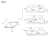
- FIG. 2 is a conceptual diagram for explaining a method of measuring the average film thickness of the titanium film.
- 3 shows the conductive material No. 1 in the example.
- 5 is a photograph of the surface of the titanium film of No. 5 observed with a scanning electron microscope (SEM).
- 4 shows the conductive material No. 1 in the example. It is the photograph of the secondary electron image which observed the cross section of 5 with the scanning electron microscope (SEM).
- FIG. 5 shows the conductive material No. in Example. 5 is a photograph of a reflected electron image obtained by observing the cross section of No. 5 with a scanning electron microscope (SEM).
- Non-Patent Document 1 has a problem that the washability after plating is poor because LiF and NaF contained in the molten salt bath hardly dissolve in water.
- the molten salt bath described in Non-Patent Document 2 and Non-Patent Document 3 is excellent in water washability, and can deposit titanium at a lower temperature than the molten salt bath described in Non-Patent Document 1, A smooth titanium film could not be obtained.
- the method described in Patent Document 1 could deposit an alloy film of Fe and Ti, but could not deposit a metal titanium film. That is, the alloy film of Fe and Ti is stable in the molten salt bath, whereas metal Ti is not sufficient in that it is dissolved into the molten salt bath by the leveling reaction.
- the method of patent document 2 and patent document 3 is a method of refining titanium, and the titanium to electrodeposit is dendritic. That is, the method described in Patent Document 2 and Patent Document 3 cannot obtain a smooth titanium film.
- the present disclosure aims to provide a conductive material having a thin titanium film on the surface with little variation in film thickness.
- the conductive material of the present disclosure has a titanium film having an average film thickness of 1 ⁇ m or more and 300 ⁇ m or less on at least the surface of a substrate having a conductive surface.
- the conductive material it is possible to provide a conductive material having a thin titanium film on the surface with little variation in film thickness.
- each of the maximum thickness and the minimum thickness of the titanium film measured at any five locations is measured. Is preferably within ⁇ 50% of the average film thickness.
- the titanium film has a titanium layer and a titanium alloy layer containing an alloy of titanium and a metal contained in the base material, and the titanium alloy layer includes a titanium layer and a base material. It is preferably located between. In this case, since the stress generated between the titanium film and the base material is relaxed, the titanium film is difficult to peel off.
- a method for producing a conductive material according to the present disclosure is a method for producing the conductive material, the molten salt bath forming step of preparing a molten salt bath containing KF, KCl, and K 2 TiF 6 , A surface of the cathode by supplying Ti into the salt bath and dissolving the Ti in the molten salt bath, and performing molten salt electrolysis using the cathode and anode provided in the molten salt bath in which Ti is dissolved
- Ti 4+ in the molten salt bath is the minimum amount necessary to become Ti 3+ by the leveling reaction represented by the following formula (1).
- a substrate having at least a conductive surface is used as the cathode.
- a conductive material having a thin titanium film on the surface with little variation in film thickness can be produced.
- the mixing ratio of KF and KCl is preferably 10:90 to 90:10 in terms of molar ratio.
- the content ratio of K 2 TiF 6 in the molten salt bath is preferably 0.1 mol% or more.
- Ti supplied in the melting step is preferably sponge titanium.
- Sponge titanium refers to a porous titanium metal having a porosity of 1% or more.
- the porosity of sponge titanium is calculated by 100 ⁇ (volume calculated from mass) / (apparent volume) ⁇ 100.
- the anode is preferably made of Ti.
- the titanium film can be stably and continuously deposited on the surface of the cathode.
- FIG. 1 is a schematic cross-sectional view showing an example of the conductive material of the embodiment.
- the conductive material 10 is a conductive material having a titanium film 12 having an average film thickness of 1 ⁇ m or more and 300 ⁇ m or less on the surface of a substrate 11 having a conductive surface at least.
- the base material 11 should just be what the surface has electroconductivity at least.
- a metal having a use for forming the titanium film 12 on the surface, a conductive sintered body, or the like can be given.
- nickel, iron, SUS304, molybdenum, tungsten, copper, carbon, or the like can be preferably used.
- the shape of the substrate 11 is not particularly limited. For example, it may have a flat plate shape, a rod shape, a cylindrical shape, or a complicated three-dimensional shape. According to the conductive material manufacturing method described later, the titanium film 12 can be easily formed on the surface of the base material 11 even if the base material 11 has a complicated three-dimensional shape.
- the titanium film 12 is located on the surface of the base material 11. Specifically, the titanium film 12 covers the surface of the base material 11. The titanium film 12 may cover the entire surface of the base material 11 or may cover a part thereof.
- the titanium film 12 has an average film thickness of 1 ⁇ m or more and 300 ⁇ m or less. The average film thickness of the titanium film 12 shall be measured as follows.
- FIG. 2 is a conceptual diagram for explaining a method of measuring the average film thickness of the titanium film.
- the conductive material 10 is divided into areas without any bias, and five locations (area 1 to area 5) are selected as measurement locations.
- the cross section of the titanium film 12 in each area is observed with a scanning electron microscope (SEM).
- SEM scanning electron microscope
- the magnification of the SEM is set so that the whole thickness direction of the titanium film 12 can be confirmed and the thickness direction can be seen as large as possible within one field of view. Then, change the field of view and observe three places in each area.
- FIG. 2 shows a conceptual diagram when three visual fields (fields 1 to 3) are observed in area 1.
- the thickness of the titanium film 12 refers to the length of the titanium film 12 extending in the vertical direction from the substrate 11.
- the maximum thickness dmax of the three visual fields and the minimum thickness dmin of the three visual fields are determined.
- the maximum thickness dmax and the minimum thickness dmin in the three visual fields are measured.
- the average value of all 15 maximum thicknesses dmax and 15 minimum thicknesses dmin measured as described above is referred to as an average film thickness of the titanium film.
- the average film thickness of the titanium film 12 is 1 ⁇ m or more, corrosion resistance and heat resistance are sufficiently exhibited.
- the conductive material 10 having the titanium film 12 can be provided at a low cost without excessively forming the titanium film 12 on the surface of the substrate 11. Can do.
- the average film thickness of the titanium film 12 is more preferably 5 ⁇ m or more and 200 ⁇ m or less, and further preferably 15 ⁇ m or more and 100 ⁇ m or less.
- the titanium film 12 is preferably a smooth film with little variation in film thickness. Since the titanium film 12 is a smooth film with little variation in film thickness, there is no portion where the film thickness of the titanium film 12 is extremely thin, so that the corrosion resistance and heat resistance of the conductive material 10 are more reliable. It becomes.
- the thickness of the titanium film 12 is a smooth film with little variation in film thickness.
- Each (all) of the maximum thickness dmax and the minimum thickness dmin of the titanium film 12 is within ⁇ 50% of the average film thickness. That is, all of the 15 maximum thicknesses dmax and the 15 minimum thicknesses dmin measured by the above-described method for measuring the average film thickness of the titanium film 12 are within ⁇ 50% of the average film thickness. That means.
- the titanium film 12 includes a titanium layer 12a and a titanium alloy layer 12b, and the titanium alloy layer 12b is preferably located between the titanium layer 12a and the substrate 11. More specifically, it is preferable that the titanium film 12 has a configuration in which a titanium alloy layer 12b and a titanium layer 12a are stacked in this order from the substrate 11 side.
- the titanium layer 12a is a layer made of only titanium (however, inevitable impurities may be included).
- the titanium alloy layer 12b is an alloy of metal and titanium contained in the substrate 11 (however, it may contain inevitable impurities).
- the metal contained in the substrate 11 means a metal that exhibits conductivity at least on the surface of the metal.
- the conductive material 10 is manufactured by plating titanium on the surface of the base material 11. Titanium plating is performed in a molten salt bath at a high temperature of about 650 ° C. Therefore, if the conductive material 10 is rapidly cooled after plating, a large stress is generated due to the difference in thermal expansion coefficient between the titanium and the substrate 11. In the case where the titanium film 12 has a configuration including the titanium layer 12a on the front surface side and the titanium alloy layer 12b on the substrate 11 side, the stress is relieved by the titanium alloy layer 12b. Thereby, peeling of the titanium film 12 from the base material 11 can be suppressed.
- the thickness of the titanium alloy layer 12b is not particularly limited, and is preferably 0.1 ⁇ m or more and 20 ⁇ m or less, for example.
- the thickness of the titanium alloy layer 12b is 0.1 ⁇ m or more, the titanium film 12 can be made more difficult to peel.
- the thickness of the titanium alloy layer 12b is 20 ⁇ m or less, it is possible to prevent the function of pure titanium from being exhibited (that is, the function due to the titanium layer 12a). From these viewpoints, the thickness of the titanium alloy layer 12b is more preferably 0.5 ⁇ m or more and 15 ⁇ m or less, and further preferably 1 ⁇ m or more and 10 ⁇ m or less.
- the titanium alloy layer 12b is preferably three layers. More specifically, the composite layer 2bc of TiNi 3 and Ni, the composite layer 2bb of TiNi and TiNi 3 and the composite layer 2ba of Ti 2 Ni and TiNi are laminated in this order on the surface of the base material 11 made of Ni.
- the titanium alloy layer 12b and the titanium layer 12a are preferably formed in this order. In this case, the buffering function for relaxing the stress generated between the titanium film 12 and the substrate 11 is enhanced.
- the titanium film 12 including the titanium alloy layer 12b can be formed on the substrate side by forming the titanium film 12 on the substrate 11 made of iron, SUS304, copper, carbon, or the like by plating. .
- the conductive material manufacturing method of the present embodiment includes a molten salt bath forming step of preparing a molten salt bath containing KF, KCl and K 2 TiF 6 , a dissolving step of dissolving Ti in the molten salt bath, And an electrolysis step of depositing Ti on the surface of the cathode by performing molten salt electrolysis using a cathode and an anode provided in a molten salt bath. Each step will be described in detail below.
- the molten salt bath forming step is a step of preparing a molten salt bath containing KF, KCl, and K 2 TiF 6 .
- KF-KCl eutectic molten salt has a lower melting point than KF or a molten salt of KCl alone and is easily soluble in water, so it provides a molten salt bath with excellent water washability when used as a molten salt bath. can do. Further, when Ti is electroplated using a molten salt bath in which K 2 TiF 6 is added to a KF—KCl eutectic molten salt, a smooth titanium film can be electrodeposited on the substrate surface.
- the mixing ratio of KF and KCl is preferably 10:90 to 90:10 in terms of molar ratio.
- the content ratio of KF in KF-KCl is 10 mol% or more, a smooth titanium film can be electrodeposited on the surface of the substrate. Further, when the content ratio of KF in KF-KCl is 90 mol% or less, the melting point can be lowered as compared with the molten salt of KF alone. From these viewpoints, the mixing ratio of KF and KCl is more preferably 20:80 to 80:20, and further preferably 40:60 to 60:40 in terms of molar ratio.
- a molten salt bath capable of electrodepositing a titanium film on the substrate surface can be obtained.
- the timing of adding K 2 TiF 6 is not particularly limited, and KF, KCl, and K 2 TiF 6 may be mixed and heated to form a molten salt bath, or KF—KCl eutectic molten salt may be mixed with KF. 2 TiF 6 may be added to form a molten salt bath.
- the content ratio of K 2 TiF 6 in the molten salt bath is preferably 0.1 mol% or more.
- a molten salt bath capable of efficiently depositing Ti on the surface of the substrate can be obtained.
- the melting step is a step of supplying Ti into the molten salt bath prepared by the molten salt bath forming step and dissolving Ti in the molten salt bath.
- the amount of Ti to be supplied may be an amount exceeding the minimum amount necessary for Ti 4+ in the molten salt bath to become Ti 3+ by the leveling reaction represented by the following formula (1).
- variation in film thickness can be formed on the surface of a base material.
- the amount of Ti supplied to the molten salt bath is more preferably twice or more of the above-mentioned minimum amount, and more preferably 3 times or more. Further, for example, it is preferable to supply Ti so that Ti is in a state of being precipitated without being completely dissolved in the molten salt bath.
- the shape of Ti to be supplied is not particularly limited, but it is preferable to use sponge titanium or titanium powder as fine as possible.
- the higher the porosity of titanium sponge the greater the specific surface area, so that it becomes easier to dissolve in the molten salt bath. For this reason, it is more preferable to use sponge titanium having a porosity of 20% or more, and it is further preferable to use sponge titanium having a porosity of 40% or more.
- the upper limit of the porosity is not particularly limited, but is considered to be about 85% from the viewpoints of ease of handling, ease of manufacture, and the like.
- the electrolysis step is a step of performing molten salt electrolysis using a cathode and an anode provided in a molten salt bath in which Ti is dissolved.
- a conductive material base material for manufacturing purposes may be used as the cathode.
- the base material only needs to have a conductive surface at least, and may be a base material in the conductive material according to the above-described embodiment.
- a titanium alloy layer can be generated on the base material side of the titanium film.
- a high-purity titanium film that does not have a titanium alloy layer that is, a titanium film composed of only a titanium layer
- a material that does not alloy with Ti in the molten salt bath is used as the base material (cathode). Can be used.
- the anode is not particularly limited as long as it is a conductive material.
- glassy carbon, titanium, or the like can be used. From the viewpoint of stably and continuously producing a titanium film, it is preferable to use an anode made of Ti.
- the atmosphere for performing the molten salt electrolysis may be a non-oxidizing atmosphere that does not form a compound with titanium.
- molten salt electrolysis may be carried out in a glove box filled with an inert gas such as argon gas or circulated.
- Current density for performing molten salt electrolysis may be set to 10 mA / cm 2 or more 500mA / cm 2 or less.
- a titanium film can be stably formed on the surface of the cathode.
- the diffusion of titanium ions in the molten salt bath is not rate-limiting, and the formed titanium film can be prevented from being blackened.
- the current density more preferably, to 50 mA / cm 2 or more 250 mA / cm 2 or less, and more preferably be 100 mA / cm 2 or more 200 mA / cm 2 or less.
- the temperature of the molten salt bath is preferably 650 ° C. or higher and 850 ° C. or lower.
- the molten salt bath can be kept in a liquid state and molten salt electrolysis can be performed stably. Moreover, it can suppress that the component of a molten salt bath evaporates and a molten salt bath becomes unstable by making the temperature of a molten salt bath into 850 degrees C or less.
- the temperature of the molten salt bath is more preferably 650 ° C. or more and 750 ° C. or less, and further preferably 650 ° C. or more and 700 ° C. or less.
- the time for performing molten salt electrolysis is not particularly limited, and may be a time for sufficiently forming a target titanium film.
- Example 1 -Molten salt bath formation process- KCl, KF and K 2 TiF 6 were mixed and heated to 650 ° C. so that the mixing ratio of KCl and KF was 55:45 in terms of molar ratio, and the concentration of K 2 TiF 6 was 0.1 mol%, and the molten salt A bath was made.
- the electroconductive material was washed with water after the electrolysis process.
- the salt adhering to the surface of the conductive material was excellent in solubility in water and could be easily removed.
- the conductive material No. 1 having a titanium film. 1 was obtained.
- Example 2 The conductive material No. 1 was the same as Example 1 except that the current density was set to 100 mA / cm 2 . 2 was produced.
- Example 3 The conductive material No. 1 was the same as Example 1 except that the concentration of K 2 TiF 6 was 2.0 mol%. 3 was produced.
- Example 4 The conductive material No. 1 was the same as Example 3 except that the current density was 100 mA / cm 2 . 4 was produced.
- Example 5 The conductive material No. 1 was the same as in Example 3 except that the current density was 150 mA / cm 2 . 5 was produced.
- Example 6 Except for the current density of 200 mA / cm 2 , the conductive material no. 6 was produced.
- Example 1 The conductive material No. 1 was the same as in Example 1 except that the melting step was not performed and the current density was 150 mA / cm 2 . 7 was produced.
- Comparative Example 2 In the same manner as in Comparative Example 1 except that the concentration of K 2 TiF 6 was 2.0 mol% and the current density was 100 mA / cm 2 , the conductive material No. 8 was produced.
- Comparative Example 3 The conductive material No. 1 was the same as Comparative Example 2 except that the current density was 150 mA / cm 2 . 9 was produced.
- Comparative Example 4 The conductive material No. 1 was the same as Comparative Example 2 except that the current density was 200 mA / cm 2 . 10 was produced.
- Comparative Example 5 The conductive material No. 1 was the same as Comparative Example 1 except that the concentration of K 2 TiF 6 was 5.0 mol%. 11 was produced.
- the conductive material No. 1-No. No. 6 was confirmed to be a silver-white titanium film on the surface of the Ni plate as the substrate.
- the conductive material No. 7-No. No. 11 had a black film formed on the surface of the Ni plate, and titanium could not be detected by XRD.
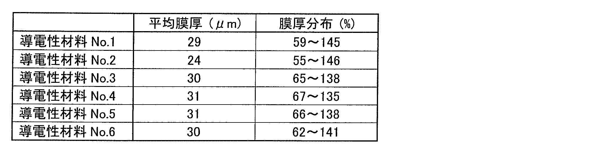
- the conductive material No. The average film thickness of the titanium film 1 was 29 ⁇ m, and it was confirmed that the maximum thickness dmax and the minimum thickness dmin were all within ⁇ 50% of the average film thickness.
- the conductive material No. 2 to No. 6 was also measured, and the average film thickness and film thickness distribution were calculated. The results are shown in Table 3 below.
- the film thickness distribution refers to the percentage of the average film thickness within the 15 maximum thicknesses dmax and 15 minimum thicknesses dmin.
- FIGS. 3 and 4 show photographs of secondary electron images obtained by observing the surface and cross section of No. 5 with a Schottky field emission scanning electron microscope (SEM) “manufactured by JEOL Ltd .: JSM-7600F”, respectively.
- the conductive material No. FIG. 5 shows a photograph of a reflected electron image obtained by observing the cross section of No. 5 with a scanning electron microscope (SEM).
- SEM scanning electron microscope
- conductive material No. 5 was subjected to composition analysis by EDX analysis (Energy Dispersive X-ray spectroscopy).
- EDX analysis was performed by point analysis of the central portion in the thickness direction of each alloy layer with an energy dispersive X-ray analyzer (EDX: X-max80 premium manufactured by OXFORD) at an acceleration voltage of 10 kV.
- the titanium alloy layer 2b has a three-layer structure. From the side close to the Ni base 1, the TiNi 3 and Ni composite layer 2bc, the TiNi and TiNi 3 composite layer 2bb, and Ti 2 Ni The TiNi composite layer 2ba was formed in this order. Further, the total thickness of the titanium alloy layer 2b is about 3 ⁇ m, the composite layer 2bc of TiNi 3 and Ni is the thickest, the composite layer 2bb of TiNi and TiNi 3 is the next thickest, and the composite layer of Ti 2 Ni and TiNi 2ba was the thinnest.
- 10 conductive material 11 base material, 12 titanium film, 12a titanium layer, 12b titanium alloy layer, 1 Ni base material, 2 titanium film, 2a titanium layer, 2b titanium alloy layer, 2ba Ti 2 Ni and TiNi composite layer, 2bb TiNi and TiNi 3 composite layer, 2bc TiNi 3 and Ni composite layer).
Landscapes
- Chemical & Material Sciences (AREA)
- Engineering & Computer Science (AREA)
- Materials Engineering (AREA)
- Metallurgy (AREA)
- Organic Chemistry (AREA)
- Chemical Kinetics & Catalysis (AREA)
- Electrochemistry (AREA)
- Mechanical Engineering (AREA)
- Electrolytic Production Of Metals (AREA)
- Electrodes For Compound Or Non-Metal Manufacture (AREA)
Abstract
Description
式(1)
3Ti4+ + Ti金属 → 4Ti3+
非特許文献1に記載されている方法は、溶融塩浴に含まれるLiFやNaFが水に殆ど溶解しないことから、めっき後の水洗性が悪いという問題があった。また、非特許文献2及び非特許文献3に記載されている溶融塩浴は水洗性に優れ、非特許文献1に記載の溶融塩浴に比べて低温でチタンを電析させることができるものの、平滑なチタン膜を得ることはできなかった。これは、非特許文献4や非特許文献5に記載されているように、平滑なチタン膜の作製にはFイオンを含む浴を使用することが効果的であり、非特許文献2のようにFイオンを含まないか、非特許文献3のようにFイオンの含有量が十分でない浴では平滑なチタン膜を得ることはできなかったと考えられる。
本開示によれば、膜厚のばらつきが少なく薄いチタン膜を表面に有する導電性材料を提供することができる。
最初に本開示の実施態様を列記して説明する。
式(1)
3Ti4+ + Ti金属 → 4Ti3+
本開示の実施態様について、以下により詳細に説明する。なお、本実施形態はこれらに限定されるものではなく、請求の範囲によって示され、請求の範囲と均等の意味および範囲内でのすべての変更が含まれることが意図される。
図1は、実施形態の導電性材料の一例を示す概略的な断面図である。図1に示されるように、導電性材料10は、少なくとも表面が導電性である基材11の表面に、平均膜厚が1μm以上300μm以下のチタン膜12を有する導電性材料である。
基材11は、少なくとも表面が導電性を有しているものであればよい。例えば、表面にチタン膜12を形成する用途のある金属や、導電性の焼結体などが挙げられる。具体的には、ニッケル、鉄、SUS304、モリブデン、タングステン、銅、カーボンなどを好ましく用いることができる。
チタン膜12は、基材11の表面に位置している。具体的には、チタン膜12は、基材11の表面を被覆している。なお、チタン膜12は、基材11の表面の全てを被覆してもよく、その一部を被覆していてもよい。チタン膜12は、1μm以上300μm以下の平均膜厚を有する。チタン膜12の平均膜厚は、以下のようにして測定されるものをいうものとする。
本実施形態の導電性材料の製造方法は、KF、KCl及びK2TiF6を含む溶融塩浴を用意する溶融塩浴形成工程と、溶融塩浴中にTiを溶解させる溶解工程と、Tiが溶解した溶融塩浴中に設けたカソード及びアノードを用いて溶融塩電解を行なうことによりカソードの表面にTiを電析させる電解工程と、を含むものである。以下に各工程を詳述する。
溶融塩浴形成工程は、KF、KCl及びK2TiF6を含む溶融塩浴を用意する工程である。
溶解工程は、溶融塩浴形成工程によって用意した溶融塩浴中にTiを供給して、溶融塩浴中にTiを溶解させる工程である。供給するTiの量は、溶融塩浴中におけるTi4+が下記式(1)で表される均化反応によりTi3+となるのに必要最低限な量を超える量とすればよい。
式(1)
3Ti4+ + Ti金属 → 4Ti3+
電解工程は、Tiが溶解した溶融塩浴中に設けたカソード及びアノードを用いて溶融塩電解を行なう工程である。Tiが溶解した溶融塩浴を溶融塩電解することでTiが電析し、カソードの表面に膜厚のばらつきが少なく薄いチタン膜を形成することができる。
前述のようにカソードの表面にチタン膜が形成されるため、カソードとしては、製造目的の導電性材料の基材を用いればよい。基材は少なくとも表面が導電性であればよく、上述した本実施形態に係る導電性材料における基材であればよい。チタンと合金化する材料を基材として用いることで、チタン膜の基材側にチタン合金層を生成させることができる。また、チタン合金層を有さない、純度の高いチタン膜(すなわち、チタン層のみからなるチタン膜)を形成させる場合には、溶融塩浴中においてTiと合金化しない材料を基材(カソード)として用いればよい。
アノードは導電性の材料であれば特に限定されるものではなく、例えば、グラッシーカーボン、チタン等を用いることができる。チタン膜を安定的に連続的に製造する観点からは、Tiからなるアノードを用いることが好ましい。
溶融塩電解を行なう雰囲気はチタンとの化合物を形成しない非酸化性雰囲気とすればよい。例えば、グローブボックス内にアルゴンガス等の不活性ガスを満たす、あるいは循環させた状態で溶融塩電解を行なえばよい。
-溶融塩浴形成工程-
KClとKFの混合比率がモル比で55:45となり、K2TiF6の濃度が0.1mol%となるようにKCl、KF及びK2TiF6を混合して650℃に加熱し、溶融塩浴を作製した。
上記の溶融塩浴形成工程で作製した溶融塩浴に、溶融塩浴1gあたりに対し13mgのスポンジチタンを添加し、十分に溶解させた。スポンジチタンとしては、空隙率が50%のものを用いた。溶融塩浴中には溶解しきらなかったスポンジチタンが沈殿した状態となった。
溶融塩電解はArフロー雰囲気のグローブボックス内で行なった。カソードとして0.5cm×2.5cm×0.1mmtのNi板を、アノードとしてTi棒を用いた。また、擬似参照極としてはPt線を用いた。そして、電流密度が25mA/cm2となるようにカソードとアノードに電圧を印加して溶融塩電解を行なった。なお、擬似参照極の電位は、Pt線上に電気化学的に析出させた金属Kの電位(K+/K電位)で較正した。その結果、カソードのNi板の表面にチタンが電析し、チタン膜を有する導電性材料を得ることができた。
電解工程後に導電性材料を水洗した。導電性材料の表面に付着した塩は水への溶解性に優れ、容易に除去することができた。以上の工程によってチタン膜を有する導電性材料No.1を得た。
電流密度を100mA/cm2とした以外は実施例1と同様にして導電性材料No.2を作製した。
K2TiF6の濃度を2.0mol%とした以外は実施例1と同様にして導電性材料No.3を作製した。
電流密度を100mA/cm2とした以外は実施例3と同様にして導電性材料No.4を作製した。
電流密度を150mA/cm2とした以外は実施例3と同様にして導電性材料No.5を作製した。
電流密度を200mA/cm2とした以外は実施例3と同様にして導電性材料No.6を作製した。
溶解工程を行なわず、かつ、電流密度を150mA/cm2とした以外は実施例1と同様にして導電性材料No.7を作製した。
K2TiF6の濃度を2.0mol%と、かつ、電流密度を100mA/cm2とした以外は比較例1と同様にして導電性材料No.8を作製した。
電流密度を150mA/cm2とした以外は比較例2と同様にして導電性材料No.9を作製した。
電流密度を200mA/cm2とした以外は比較例2と同様にして導電性材料No.10を作製した。
K2TiF6の濃度を5.0mol%とした以外は比較例1と同様にして導電性材料No.11を作製した。
導電性材料No.1~No.11を以下のようにして評価した。
導電性材料No.1~No.11の基材の表面に形成された膜の外観を目視により観察し、また、XRD(X-Ray Diffraction)により当該膜中のチタンの有無を調べた。その結果を下記表1に示す。

上述の方法にしたがって、得られた導電性材料No.1のチタン膜の最大厚みdmax及び最小厚みdminを測定した。その結果を下記表2に示す。
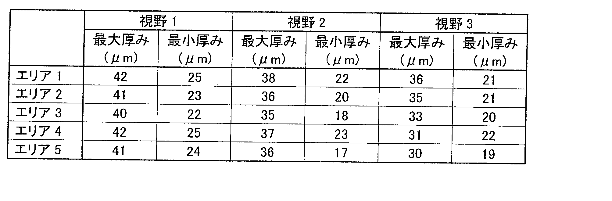
導電性材料No.5の表面及び断面をショットキー電界放射型走査型電子顕微鏡(SEM)「日本電子株式会社製:JSM-7600F」によって観察した二次電子像の写真をそれぞれ図3及び図4に示す。また、導電性材料No.5の断面を走査型電子顕微鏡(SEM)にて観察した反射電子像の写真を図5に示す。断面加工は、導電性材料を樹脂に包埋し、機械研磨及びクロスセクションポリッシャによって行なった。
Claims (8)
- 少なくとも表面が導電性である基材の表面に、平均膜厚が1μm以上300μm以下であるチタン膜を有する、導電性材料。
- 前記導電性材料の表面における任意の5箇所で前記チタン膜の厚みを測定した場合に、
前記任意の5箇所において測定されるチタン膜の最大厚みのそれぞれと最小厚みのそれぞれとが前記平均膜厚の±50%以内である、請求項1に記載の導電性材料。 - 前記チタン膜は、チタン層と、前記基材に含まれる金属とチタンとの合金を含むチタン合金層とを有し、
前記チタン合金層は、前記チタン層と前記基材との間に位置する、請求項1又は請求項2に記載の導電性材料。 - 請求項1から請求項3のいずれか1項に記載の導電性材料の製造方法であって、
KF、KCl及びK2TiF6を含む溶融塩浴を用意する溶融塩浴形成工程と、
前記溶融塩浴中にTiを供給して、前記溶融塩浴中に前記Tiを溶解させる溶解工程と、
前記Tiが溶解した前記溶融塩浴中に設けたカソード及びアノードを用いて溶融塩電解を行なうことにより前記カソードの表面にTiを電析させる電解工程と、
を含み、
前記溶解工程においては、前記溶融塩浴中におけるTi4+が下記式(1)で表される均化反応によりTi3+となるのに必要最低限な量を超える量のTiを供給し、
前記電解工程においては、前記カソードとして、少なくとも表面が導電性である基材を用いる、導電性材料の製造方法。
式(1)
3Ti4+ + Ti金属 → 4Ti3+ - 前記KFと前記KClの混合比率は、モル比で10:90~90:10である、請求項4に記載の導電性材料の製造方法。
- 前記溶融塩浴においてK2TiF6の含有比率は、0.1mol%以上である、請求項4又は請求項5に記載の導電性材料の製造方法。
- 前記溶解工程において供給される前記Tiがスポンジチタンである、請求項4から請求項6のいずれか1項に記載の導電性材料の製造方法。
- 前記アノードはTiからなる、請求項4から請求項7のいずれか1項に記載の導電性材料の製造方法。
Priority Applications (5)
| Application Number | Priority Date | Filing Date | Title |
|---|---|---|---|
| US16/085,725 US20190093249A1 (en) | 2016-03-18 | 2017-02-27 | Conductive material and method for manufacturing the same |
| JP2018505776A JP6802255B2 (ja) | 2016-03-18 | 2017-02-27 | 導電性材料及びその製造方法 |
| KR1020187026591A KR20180124043A (ko) | 2016-03-18 | 2017-02-27 | 도전성 재료 및 그의 제조 방법 |
| EP17766327.5A EP3431635A4 (en) | 2016-03-18 | 2017-02-27 | CONDUCTIVE MATERIAL AND METHOD FOR THE PRODUCTION THEREOF |
| CN201780018209.2A CN108884582A (zh) | 2016-03-18 | 2017-02-27 | 导电材料及其制造方法 |
Applications Claiming Priority (4)
| Application Number | Priority Date | Filing Date | Title |
|---|---|---|---|
| JP2016055432 | 2016-03-18 | ||
| JP2016-055432 | 2016-03-18 | ||
| JP2016128561 | 2016-06-29 | ||
| JP2016-128561 | 2016-06-29 |
Publications (1)
| Publication Number | Publication Date |
|---|---|
| WO2017159324A1 true WO2017159324A1 (ja) | 2017-09-21 |
Family
ID=59851537
Family Applications (1)
| Application Number | Title | Priority Date | Filing Date |
|---|---|---|---|
| PCT/JP2017/007520 Ceased WO2017159324A1 (ja) | 2016-03-18 | 2017-02-27 | 導電性材料及びその製造方法 |
Country Status (6)
| Country | Link |
|---|---|
| US (1) | US20190093249A1 (ja) |
| EP (1) | EP3431635A4 (ja) |
| JP (1) | JP6802255B2 (ja) |
| KR (1) | KR20180124043A (ja) |
| CN (1) | CN108884582A (ja) |
| WO (1) | WO2017159324A1 (ja) |
Cited By (4)
| Publication number | Priority date | Publication date | Assignee | Title |
|---|---|---|---|---|
| WO2018216321A1 (ja) * | 2017-05-22 | 2018-11-29 | 住友電気工業株式会社 | 金属多孔体及び金属多孔体の製造方法 |
| WO2018216322A1 (ja) * | 2017-05-22 | 2018-11-29 | 住友電気工業株式会社 | 複合金属多孔体及び複合金属多孔体の製造方法 |
| WO2019171744A1 (ja) * | 2018-03-08 | 2019-09-12 | 住友電気工業株式会社 | チタンめっき部材の製造方法及びチタンめっき部材 |
| WO2020217603A1 (ja) * | 2019-04-26 | 2020-10-29 | 住友電気工業株式会社 | チタン含有部材の製造方法 |
Citations (6)
| Publication number | Priority date | Publication date | Assignee | Title |
|---|---|---|---|---|
| JPS6431990A (en) * | 1987-07-29 | 1989-02-02 | Nisshin Steel Co Ltd | Titanium electroplating bath and plating method using same |
| JPH04173996A (ja) * | 1990-11-05 | 1992-06-22 | Tokin Corp | 絶縁性高透磁率合金の製造方法 |
| JPH08225980A (ja) | 1995-12-01 | 1996-09-03 | Japan Energy Corp | 高純度チタンを製造する方法及び装置 |
| JPH08246130A (ja) * | 1995-03-06 | 1996-09-24 | Nkk Corp | チタンめっきステンレス鋼板 |
| JPH0971890A (ja) | 1995-09-05 | 1997-03-18 | Toho Titanium Co Ltd | 高純度チタンの製造方法 |
| JP2015193899A (ja) | 2013-11-19 | 2015-11-05 | 住友電気工業株式会社 | 電析用電解質および金属膜の製造方法 |
Family Cites Families (2)
| Publication number | Priority date | Publication date | Assignee | Title |
|---|---|---|---|---|
| US7410562B2 (en) * | 2003-08-20 | 2008-08-12 | Materials & Electrochemical Research Corp. | Thermal and electrochemical process for metal production |
| CN103060862B (zh) * | 2012-12-26 | 2015-08-12 | 广东电网公司电力科学研究院 | 钛涂层及其制备方法 |
-
2017
- 2017-02-27 WO PCT/JP2017/007520 patent/WO2017159324A1/ja not_active Ceased
- 2017-02-27 US US16/085,725 patent/US20190093249A1/en not_active Abandoned
- 2017-02-27 KR KR1020187026591A patent/KR20180124043A/ko not_active Ceased
- 2017-02-27 CN CN201780018209.2A patent/CN108884582A/zh active Pending
- 2017-02-27 JP JP2018505776A patent/JP6802255B2/ja active Active
- 2017-02-27 EP EP17766327.5A patent/EP3431635A4/en active Pending
Patent Citations (6)
| Publication number | Priority date | Publication date | Assignee | Title |
|---|---|---|---|---|
| JPS6431990A (en) * | 1987-07-29 | 1989-02-02 | Nisshin Steel Co Ltd | Titanium electroplating bath and plating method using same |
| JPH04173996A (ja) * | 1990-11-05 | 1992-06-22 | Tokin Corp | 絶縁性高透磁率合金の製造方法 |
| JPH08246130A (ja) * | 1995-03-06 | 1996-09-24 | Nkk Corp | チタンめっきステンレス鋼板 |
| JPH0971890A (ja) | 1995-09-05 | 1997-03-18 | Toho Titanium Co Ltd | 高純度チタンの製造方法 |
| JPH08225980A (ja) | 1995-12-01 | 1996-09-03 | Japan Energy Corp | 高純度チタンを製造する方法及び装置 |
| JP2015193899A (ja) | 2013-11-19 | 2015-11-05 | 住友電気工業株式会社 | 電析用電解質および金属膜の製造方法 |
Non-Patent Citations (6)
| Title |
|---|
| A. ROBIN: "Electrolytic Coating of Titanium onto Iron and Nickel Electrodes in the Molten LiF + NaF + KF Eutectic", JOURNAL OF ELECTROANALYTICAL CHEMISTRY AND INTERFACIAL ELECTROCHEMISTRY, vol. 230, 1987, pages 125 - 141, XP026763330, DOI: doi:10.1016/0022-0728(87)80137-7 |
| DAWEI WEI ET AL.: "Characteristics of Ti Films Electrodeposited from Molten Salts by a Pulse Current Method", JOURNAL OF THE JAPAN INSTITUTE OF METALS AND MATERIALS, vol. 58, no. 6, 1994, pages 660 - 667 |
| HIROSHI TAKAMURA ET AL.: "Smooth and Fine Electrodeposition of Titanium from LiCl-KCl-TiCl Melt", JOURNAL OF THE JAPAN INSTITUTE OF METALS AND MATERIALS, vol. 60, no. 4, 1996, pages 388 - 397 |
| JIANXUN SONG: "The Influence of Fluoride Anion on the Equilibrium between Titanium Ions and Electrodeposition of Titanium in Molten Fluoride-Chloride Salt", MATERIALS TRANSACTIONS, vol. 55, no. 8, 2014, pages 1299 - 1303 |
| See also references of EP3431635A4 |
| YANG SONG, THE CATHODIC BEHAVIOR OF TI(III) ION IN A NACL-2CSCL MELT'', METALLURGICAL AND MATERIALS TRANSACTIONS B, vol. 47B, February 2016 (2016-02-01), pages 804 - 810 |
Cited By (7)
| Publication number | Priority date | Publication date | Assignee | Title |
|---|---|---|---|---|
| WO2018216321A1 (ja) * | 2017-05-22 | 2018-11-29 | 住友電気工業株式会社 | 金属多孔体及び金属多孔体の製造方法 |
| WO2018216322A1 (ja) * | 2017-05-22 | 2018-11-29 | 住友電気工業株式会社 | 複合金属多孔体及び複合金属多孔体の製造方法 |
| WO2019171744A1 (ja) * | 2018-03-08 | 2019-09-12 | 住友電気工業株式会社 | チタンめっき部材の製造方法及びチタンめっき部材 |
| JPWO2019171744A1 (ja) * | 2018-03-08 | 2021-03-11 | 住友電気工業株式会社 | チタンめっき部材の製造方法及びチタンめっき部材 |
| JP7086172B2 (ja) | 2018-03-08 | 2022-06-17 | 住友電気工業株式会社 | チタンめっき部材の製造方法及びチタンめっき部材 |
| WO2020217603A1 (ja) * | 2019-04-26 | 2020-10-29 | 住友電気工業株式会社 | チタン含有部材の製造方法 |
| JPWO2020217603A1 (ja) * | 2019-04-26 | 2020-10-29 |
Also Published As
| Publication number | Publication date |
|---|---|
| EP3431635A4 (en) | 2019-08-07 |
| JPWO2017159324A1 (ja) | 2019-01-24 |
| JP6802255B2 (ja) | 2020-12-16 |
| US20190093249A1 (en) | 2019-03-28 |
| EP3431635A1 (en) | 2019-01-23 |
| KR20180124043A (ko) | 2018-11-20 |
| CN108884582A (zh) | 2018-11-23 |
Similar Documents
| Publication | Publication Date | Title |
|---|---|---|
| US11757101B2 (en) | Metal porous body and method for producing metal porous body | |
| Gu et al. | Electrodeposition of alloys and compounds from high-temperature molten salts | |
| EP3633079A1 (en) | Composite metal porous body and method for producing composite metal porous body | |
| JP6405199B2 (ja) | 電析用電解質および金属膜の製造方法 | |
| JP6802255B2 (ja) | 導電性材料及びその製造方法 | |
| US20020092585A1 (en) | Deposition and thermal diffusion of borides and carbides of refractory metals | |
| WO2017199564A1 (ja) | アルミニウム合金及びアルミニウム合金の製造方法 | |
| US20210087701A1 (en) | Aluminum plating film and method for producing aluminum plating film | |
| US10941499B2 (en) | Electrodeposition of Al—Ni alloys and Al/Ni multilayer structures | |
| JP6889447B2 (ja) | チタンめっき液の製造方法及びチタンめっき製品の製造方法 | |
| Kan et al. | Electrodeposition of aluminum and aluminum—magnesium alloys at room temperature | |
| Mehmood et al. | Electro-deposition of tantalum on tungsten and nickel in LiF-NaF-CaF2 melt containing K2TaF7—Electrochemical study | |
| Arai et al. | Fabrication of Ag-Bi alloy films from an iodide-tartrate bath via current pulse electrodeposition | |
| Hrussanova et al. | Properties of silver-tin alloys obtained from pyrophosphate-cyanide electrolytes containing EDTA salts | |
| JP7516903B2 (ja) | アルミニウム箔の製造方法 | |
| Rooksby | The X-Ray Structure of Speculum Electrodeposits | |
| Fekih et al. | The iron-nickel-molybdenum (Fe-Ni-Mo) electrodeposited alloy on n-type silicon | |
| JP2018003072A (ja) | タングステン膜及びタングステン膜の製造方法 | |
| Lee et al. | Temperature and Concentration Dependencies of LiF-NaF-K2TaF7 Phase Equilibria and Effects on Ta Electrodeposition Layer | |
| KR101431336B1 (ko) | 용융염 다중 양극 반응 합금 도금법(marc)을 이용한 탄탈룸 합금 코팅 피막 형성 방법 및 이에 의해 제조된 구조재 | |
| Barral et al. | Preparation of composition-modulated films by alternate electrodeposition from different electrolytes | |
| JP3360058B2 (ja) | 耐高温酸化性に優れた皮膜を有する耐熱性金属部材およびその製造方法 | |
| JPH0551784A (ja) | Ti−Al合金薄膜およびその製造方法 | |
| WO2020217603A1 (ja) | チタン含有部材の製造方法 | |
| Sheu et al. | Substrate interaction effects on the structure of chromium electrodeposits |
Legal Events
| Date | Code | Title | Description |
|---|---|---|---|
| WWE | Wipo information: entry into national phase |
Ref document number: 2018505776 Country of ref document: JP |
|
| ENP | Entry into the national phase |
Ref document number: 20187026591 Country of ref document: KR Kind code of ref document: A |
|
| NENP | Non-entry into the national phase |
Ref country code: DE |
|
| WWE | Wipo information: entry into national phase |
Ref document number: 2017766327 Country of ref document: EP |
|
| ENP | Entry into the national phase |
Ref document number: 2017766327 Country of ref document: EP Effective date: 20181018 |
|
| 121 | Ep: the epo has been informed by wipo that ep was designated in this application |
Ref document number: 17766327 Country of ref document: EP Kind code of ref document: A1 |