WO2017159594A1 - Élément de conversion thermoélectrique et module de conversion thermoélectrique - Google Patents
Élément de conversion thermoélectrique et module de conversion thermoélectrique Download PDFInfo
- Publication number
- WO2017159594A1 WO2017159594A1 PCT/JP2017/009920 JP2017009920W WO2017159594A1 WO 2017159594 A1 WO2017159594 A1 WO 2017159594A1 JP 2017009920 W JP2017009920 W JP 2017009920W WO 2017159594 A1 WO2017159594 A1 WO 2017159594A1
- Authority
- WO
- WIPO (PCT)
- Prior art keywords
- thermoelectric
- metal layer
- thermoelectric conversion
- conversion element
- insulator
- Prior art date
- Legal status (The legal status is an assumption and is not a legal conclusion. Google has not performed a legal analysis and makes no representation as to the accuracy of the status listed.)
- Ceased
Links
Images




Classifications
-
- H—ELECTRICITY
- H02—GENERATION; CONVERSION OR DISTRIBUTION OF ELECTRIC POWER
- H02N—ELECTRIC MACHINES NOT OTHERWISE PROVIDED FOR
- H02N11/00—Generators or motors not provided for elsewhere; Alleged perpetua mobilia obtained by electric or magnetic means
-
- H—ELECTRICITY
- H10—SEMICONDUCTOR DEVICES; ELECTRIC SOLID-STATE DEVICES NOT OTHERWISE PROVIDED FOR
- H10N—ELECTRIC SOLID-STATE DEVICES NOT OTHERWISE PROVIDED FOR
- H10N10/00—Thermoelectric devices comprising a junction of dissimilar materials, i.e. devices exhibiting Seebeck or Peltier effects
- H10N10/01—Manufacture or treatment
-
- H—ELECTRICITY
- H10—SEMICONDUCTOR DEVICES; ELECTRIC SOLID-STATE DEVICES NOT OTHERWISE PROVIDED FOR
- H10N—ELECTRIC SOLID-STATE DEVICES NOT OTHERWISE PROVIDED FOR
- H10N10/00—Thermoelectric devices comprising a junction of dissimilar materials, i.e. devices exhibiting Seebeck or Peltier effects
- H10N10/10—Thermoelectric devices comprising a junction of dissimilar materials, i.e. devices exhibiting Seebeck or Peltier effects operating with only the Peltier or Seebeck effects
- H10N10/17—Thermoelectric devices comprising a junction of dissimilar materials, i.e. devices exhibiting Seebeck or Peltier effects operating with only the Peltier or Seebeck effects characterised by the structure or configuration of the cell or thermocouple forming the device
-
- H—ELECTRICITY
- H10—SEMICONDUCTOR DEVICES; ELECTRIC SOLID-STATE DEVICES NOT OTHERWISE PROVIDED FOR
- H10N—ELECTRIC SOLID-STATE DEVICES NOT OTHERWISE PROVIDED FOR
- H10N10/00—Thermoelectric devices comprising a junction of dissimilar materials, i.e. devices exhibiting Seebeck or Peltier effects
- H10N10/80—Constructional details
- H10N10/81—Structural details of the junction
- H10N10/817—Structural details of the junction the junction being non-separable, e.g. being cemented, sintered or soldered
-
- H—ELECTRICITY
- H10—SEMICONDUCTOR DEVICES; ELECTRIC SOLID-STATE DEVICES NOT OTHERWISE PROVIDED FOR
- H10N—ELECTRIC SOLID-STATE DEVICES NOT OTHERWISE PROVIDED FOR
- H10N10/00—Thermoelectric devices comprising a junction of dissimilar materials, i.e. devices exhibiting Seebeck or Peltier effects
- H10N10/80—Constructional details
- H10N10/85—Thermoelectric active materials
- H10N10/851—Thermoelectric active materials comprising inorganic compositions
- H10N10/852—Thermoelectric active materials comprising inorganic compositions comprising tellurium, selenium or sulfur
-
- H—ELECTRICITY
- H10—SEMICONDUCTOR DEVICES; ELECTRIC SOLID-STATE DEVICES NOT OTHERWISE PROVIDED FOR
- H10N—ELECTRIC SOLID-STATE DEVICES NOT OTHERWISE PROVIDED FOR
- H10N10/00—Thermoelectric devices comprising a junction of dissimilar materials, i.e. devices exhibiting Seebeck or Peltier effects
- H10N10/80—Constructional details
- H10N10/85—Thermoelectric active materials
- H10N10/851—Thermoelectric active materials comprising inorganic compositions
- H10N10/853—Thermoelectric active materials comprising inorganic compositions comprising arsenic, antimony or bismuth
Definitions
- the present invention relates to a thermoelectric conversion element and a thermoelectric conversion module.
- thermoelectric conversion elements using the Seebeck effect or Peltier effect are used for the thermoelectric conversion module.
- This thermoelectric conversion element has attracted attention in recent years because it has a simple structure, is easy to handle, and can maintain stable characteristics. In particular, it can be used to recover waste heat from a garbage disposal site or to cool a laser diode.
- Patent Document 1 discloses a thermoelectric conversion module used for cooling applications utilizing the Peltier effect as described above.
- a thermoelectric conversion module described in Patent Document 1 a p-type thermoelectric conversion element 50-p having p-type characteristics and an n-type thermoelectric conversion element 50-n having n-type characteristics are joined as shown in FIG.
- a configuration is disclosed in which a plurality of pn element pairs are arranged in series by bonding via an electrode 50-1 and solder or the like. Extraction terminals 60-1 and 60-1 'are connected to the junction electrodes 50-1 at both ends of the series arrangement, respectively. Further, the bonding electrode 50-1 is sandwiched between the high temperature side ceramic substrate 50-2H and the low temperature side ceramic substrate 50-2C which are a pair of wiring substrates from the outside.
- thermoelectric conversion module is used for cooling by bringing the low temperature side ceramic substrate 50-2C into contact with the object to be cooled.
- thermoelectric conversion element 50-p and the n-type thermoelectric conversion element 50-n are expressed by the Seebeck coefficient ⁇ , the specific resistance ⁇ , and the thermal conductivity K, which are constants specific to the substance, in the temperature range of use.
- a BiTe-based material is generally used as a thermoelectric member.
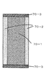
- thermoelectric member 70-1 sandwiched between the metal films 70-3 is made of glass or epoxy as shown in FIG. It is known that an insulator 70-2 formed of an insulating material such as a resin is formed around (Patent Document 2).
- thermoelectric member tends to extend more than the insulator because it is a modularized process under a usage environment of nearly 100 ° C. and 300 ° C. or higher. Therefore, there is a problem that a large stress is generated in the insulating material, and the insulating material is damaged during use or after completion of the module.
- the present invention solves the above-described problems and aims to provide a high-quality thermoelectric conversion element and thermoelectric conversion module that do not damage the insulating material itself.
- thermoelectric conversion element includes a columnar thermoelectric member, an insulator formed around the thermoelectric member, and a metal formed continuously on an end surface of the thermoelectric member and an end surface of the insulator.
- a gap is formed between an end portion of the thermoelectric member and an end portion of the insulator, and the gap is covered with the metal layer, and the gap is covered with the metal layer. Is a void.
- the metal layer may be formed from the end side of the gap toward the inside.
- the metal layer may be formed on an end surface of the thermoelectric member, an end portion side of the thermoelectric member and an end portion side of the insulator in the gap.
- the volume of the first gap formed on the end side of the thermoelectric member may be larger than the volume of the second gap formed on the center side in the longitudinal direction of the thermoelectric member.
- the metal layer may be composed of a plurality of layers.
- the plurality of metal layers include a first metal layer on the thermoelectric member side and a second metal layer formed on the opposite side of the first metal layer to the thermoelectric member side,
- the density of Ni in the first metal layer may be greater than the density of Ni in the second metal layer.
- the thickness of the first metal layer may be 5 nm to 1 ⁇ m.
- a high adhesion layer having higher adhesion than the Ni layer may be included between the first metal layer and the thermoelectric member.
- the high adhesion layer may be made of Ti, Mo, Cr, or TiN.
- thermoelectric conversion element is continuous with a columnar thermoelectric member, an insulator formed in a cylindrical shape around the thermoelectric member, an end surface of the thermoelectric member, and an end surface of the insulator. And the end surface of the insulator protrudes beyond the end surface of the thermoelectric member.
- thermoelectric conversion module includes a first wiring board, a second wiring board facing the first wiring board, the first wiring board, and the second wiring board. Between the thermoelectric conversion elements according to any one of the above.
- thermoelectric conversion element and the thermoelectric conversion module according to the present invention can provide a high-quality thermoelectric conversion element without cracks or cracks in the insulator.
- FIG. 1 is a cross-sectional view of a thermoelectric conversion element according to an embodiment.
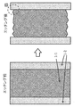
- FIG. 2 is an enlarged view of a portion A in FIG. Drawing 3 is a figure showing shape change before and behind etching of a thermoelectric conversion element concerning an embodiment.
- FIG. 4 is an enlarged view of a portion B in FIG.
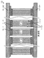
- FIG. 5 is a cross-sectional view of the thermoelectric conversion module according to the embodiment.
- FIG. 6 is a perspective view of a conventional thermoelectric conversion module.
- FIG. 7 is a cross-sectional view of a conventional thermoelectric conversion element.
- FIG. 1 is a cross-sectional view of a thermoelectric conversion element 1 according to the present embodiment.
- the thermoelectric conversion element 1 includes a columnar thermoelectric member 1-1, an insulator 1-2 formed around the thermoelectric member 1-1, and an electrode that is in close contact with the thermoelectric member 1-1 and the insulator 1-2. And a metal layer 1-3.
- thermoelectric member 1-1 can generate a temperature difference at the end face of the thermoelectric conversion element 1 when an electric current is passed, and can pass an electric current when a temperature difference is generated at the end face of the thermoelectric conversion element 1.
- columnar members having such thermoelectric conversion characteristics as p-type thermoelectric members and n-type thermoelectric members.
- thermoelectric member a BiTe-based material is generally used for both p-type and n-type. Specifically, Bi 0.5 Sb 1.5 Te 3 doped with Sb is used as the p-type thermoelectric member, and Bi 2 Te 2.7 Se doped with Se as the n-type thermoelectric member. 0.3 is used.
- thermoelectric member 1-1 it is desirable that these BiTe-based materials are used as the thermoelectric member 1-1.
- the material has thermoelectric conversion characteristics, for example, a CoSb-based material, a PdTe-based material, and a MnSi-based material.
- the material can be applied, and the material is not particularly limited.
- a general composition of a BiTe-based material is added with various elements for further improvement of thermoelectric characteristics, and a binder such as carbon nanotube, fullerene, or glass frit is used for material strengthening. May be included.
- thermoelectric conversion element 1 is not particularly limited to a shape such as a prismatic shape or a cylindrical shape, but a cylindrical shape is desirable in consideration of an effect of reducing stress concentration.
- the material of the insulator 1-2 is not particularly limited to an inorganic material such as ceramic and glass, and a polymer material typified by epoxy as long as it is an insulator material.
- quartz glass, heat-resistant glass a kind of borosilicate glass in which SiO 2 and B 2 O 3 are mixed, a material having an expansion coefficient of about 3 ⁇ 10 ⁇ 6 / K
- Pyrex manufactured by Corning (Registered trademark) or the like is preferably used.
- the thickness of the insulator 1-2 is not particularly limited, but in the thermoelectric conversion element 1 or the thermoelectric conversion module, the presence of the insulator 1-2 adversely affects the characteristics, so it is desirable that the insulator 1-2 be as thin as possible.
- the thickness of the insulator 1-2 is preferably within 0.01 mm to 10 mm. Furthermore, it is desirable to be 0.015 mm to 3 mm.
- the width S and the height L of the tubular thermoelectric conversion element 1 are not particularly limited because they are items designed according to the electrical performance of each module and the size restrictions in use.
- the width S is desirably 0.1 mm to 10 mm
- the height L is desirably 0.1 mm to 10 mm.
- one end face 1-8 of the insulator 1-2 protrudes from one end face 1-7 of the thermoelectric member 1-1. Further, the other end face 1-8 'of the insulator 1-2 protrudes from one end face 1-7' of the thermoelectric member 1-1. This increases the contact area between the solder used for bonding to the substrate electrode and the end face of the thermoelectric conversion element 1 when modularization is performed after the metal layer 1-3 or the like is formed, and reliability is improved. It is for improving.
- thermoelectric conversion element in a state where there is no step between the end surface is formed.
- thermoelectric member 1-1 is dissolved using an etching solution such as sulfuric acid, nitric acid, hydrogen peroxide solution, and ammonium fluoride that can dissolve the thermoelectric member 1-1.
- an etching solution such as sulfuric acid, nitric acid, hydrogen peroxide solution, and ammonium fluoride that can dissolve the thermoelectric member 1-1.
- etching solution such as sulfuric acid, nitric acid, hydrogen peroxide solution, and ammonium fluoride that can dissolve the thermoelectric member 1-1.
- one end face 1-8 and the other end face 1-8 'of the insulator 1-2 can be projected.
- the type of the etching solution is not limited as long as it can be subsequently removed by washing.
- thermoelectric member 1-1 When the thermoelectric member 1-1 is dissolved using the etching solution, not only the one end surface 1-7 and the other end surface 1-7 ′ of the thermoelectric member 1-1 are dissolved, but also the thermoelectric member 1 -1 and the insulator 1-2 are infiltrated with the etching solution by capillary action. For this reason, dissolution proceeds more positively at the interface.
- thermoelectric member end portion 2-2 there is a gap V between the thermoelectric member end portion 2-2 and the insulator end portion 2-3 at the interface between the thermoelectric member 1-1 and the insulator 1-2.
- the groove 4-1 can be formed.
- the metal layer 1-3 is continuously formed on one end surface 1-7 of the thermoelectric member 1-1 and one end surface 1-8 of the insulator 1-2. ing. As a result, a gap 2-1 is secured at the interface between the thermoelectric member 1-1 and the insulator 1-2.
- thermoelectric member 1-1 and the insulator 1-2 Due to the presence of the air gap 2-1, even in the case where the thermoelectric member 1-1 and the insulator 1-2 have different expansion coefficients, in the use environment where the temperature is close to 100 ° C. and in the modularization process where the temperature becomes 300 ° C. When the thermoelectric member is about to extend beyond the insulator, the stress generated in the insulator 1-2 can be relaxed. Therefore, it is possible to prevent the insulator 1-2 from being damaged.
- the metal layer 1-3 is preferably formed from the end face side of the gap 2-1 toward the inside.
- the contact area between the thermoelectric member 1-1 and the metal layer 1-3 is increased as compared with the structure without the air gap 2-1, so that the adhesion between the thermoelectric member 1-1 and the metal layer 1-3 is increased. Can be increased.
- the decrease in the adhesion between the thermoelectric member 1-1 and the metal layer 1-3 due to the gap 2-1 can be greatly reduced.
- the material of the metal layer 1-3 has no problem in the function as a barrier film for preventing the reaction between the BiTe-based material and the solder material used in the subsequent modularization, and the bonding with the solder material.
- the element type is not particularly limited, and a single metal or an alloy may be used.
- the metal layer 1-3 is preferably composed of a plurality of layers, and the metal type is preferably a metal film mainly composed of Ni having excellent barrier properties.
- a metal layer 1-5 that is a high Ni density layer is formed on the side close to the end face of the thermoelectric member 1-1, and a metal layer that is a low density Ni layer is formed on the side far from the end face of the thermoelectric member 1-1. It is desirable that 1-6 is formed.
- the metal layer 1-5 is formed by a sputtering method, a vapor deposition method, a thermal spraying method, an electrolytic plating method, or the like, and the element ratio of Ni is 99% or more. As a result, the metal layer 1-5 can be formed as a dense and stable film.
- the thickness of the metal layer 1-5 is desirably 5 nm to 1 ⁇ m.
- the metal layer 1-5 is dense, it tends to peel off due to large film stress, and if it is formed thicker than 1 ⁇ m, the film may peel off.
- the thermoelectric conversion element 1 is modularized, Ni disappears if the metal layer 1-5 is thin due to thermal diffusion caused by the heat of the solder used to join the thermoelectric conversion element 1 and the substrate. Therefore, the thickness of Ni needs to be larger than 1 ⁇ m.
- the metal layer 1-6 is formed on the metal layer 1-5 by electroless plating with a low Ni element ratio and a small internal stress.
- the thickness of the metal layer 1-6 is desirably 100 nm to 100 ⁇ m.
- the thickness of the metal layer 1-6 is 100 nm or less, the effect of increasing the Ni thickness by the metal layer 1-6 is not so much, and a part of Ni may be lost.
- the thickness of the metal layer 1-6 is larger than 100 ⁇ m, the plating grows not only in the thickness direction but also in the lateral direction, and thus grows greatly beyond the insulator 1-2. There is a risk of problems such as short circuit in the module process.
- Ni by electroless plating contains P and B in addition to Ni, but any element may be included.
- the plating proceeds using the Ni element of the metal layer 1-5 as a catalyst.
- the thickness of the metal layer 1-5 is desirably 5 nm or more.
- a high adhesion layer 1-4 having higher adhesion than the Ni layer is formed between the metal layer 1-5 and the thermoelectric member 1-1.
- the high adhesion layer 1-4 is composed of one or more of Ti, Mo, TiN, and Cr that can be strongly bonded to the thermoelectric member 1-1 even in a state where this oxidation state remains.
- the high adhesion layer 1-4 is formed by a sputtering method. It is desirable to form by a vacuum process such as vapor deposition or vacuum spraying.
- Ti is not only highly adhesive, but also has very high barrier properties, and is particularly preferable as a highly adhesive layer.
- thermoelectric member 1-1 and the metal layer 1-3 can be firmly adhered to each other.
- thermoelectric conversion element 1 in which the insulator 1-2 is not cracked or broken.
- FIG. 5 shows a thermoelectric conversion module 10 according to the present embodiment using the thermoelectric conversion element 1 formed by the above configuration.
- the structure of the thermoelectric conversion module 10 shown in FIG. 5 is a pi-type structure, and the p-type thermoelectric conversion element 5-p and the n-type thermoelectric conversion element 5- having the structure of the thermoelectric conversion element 1 according to the present embodiment. n are arranged in series.
- the pie-type structure is a structure adopted in the most general thermoelectric conversion module.
- a pie-type structure is used for description.
- the structure may be determined according to various uses such as a half skeleton structure and a skeleton structure, and the thermoelectric conversion module according to the present invention. Is not limited to the pie structure.
- thermoelectric elements are connected to the bonding electrode 5-1 using a bonding material such as AuSn solder or SnAgCu solder.
- a bonding material such as AuSn solder or SnAgCu solder.
- the bonding material depends on the use environment of the thermoelectric conversion module 10 and the manufacturing process of the set product to be applied thereafter, and the material is not particularly limited as long as an excellent electrical connection is possible.
- the bonding electrode 5-1 is formed on the low-temperature side ceramic substrate 5-2C and the high-temperature side ceramic substrate 5-2H, which are wiring substrates, and Cu, Al, or the like is formed using a plating method or a vapor deposition method. It is a part that is wired. Also, the bonding electrode 5-1 is not particularly limited, although Cu is generally used.
- alumina and silicon nitride are generally used for the low temperature side ceramic substrate 5-2C and the high temperature side ceramic substrate 5-2H, but the material is not limited.
- the substrate is not limited to ceramic, and in a use environment, a metal substrate such as a Cu substrate or a substrate mainly composed of an organic substance such as an epoxy substrate can be used.
- thermoelectric conversion module 10 it is possible to realize a high-quality thermoelectric conversion module 10 in which the insulator 1-2 is not cracked or chipped.
- the present invention can be widely applied when cooling is required in various technical fields.
Landscapes
- Chemical & Material Sciences (AREA)
- Inorganic Chemistry (AREA)
- Engineering & Computer Science (AREA)
- Manufacturing & Machinery (AREA)
- Cooling Or The Like Of Semiconductors Or Solid State Devices (AREA)
- Powder Metallurgy (AREA)
Abstract
L'invention porte sur un élément de conversion thermoélectrique (1) qui comprend : un élément thermoélectrique en colonne (1-1) ; un corps isolant (1-2) formé autour de l'élément thermoélectrique (1-1) ; et une couche métallique (1-3) formée de façon continue sur une surface d'extrémité de l'élément thermoélectrique (1-1) et une surface d'extrémité du corps isolant (1-2). Un espace est formé entre une partie d'extrémité de l'élément thermoélectrique (1-1) et une partie d'extrémité du corps isolant (1-2), et l'intérieur de l'espace qui est couvert par la couche métallique (1-3) constitue un vide.
Priority Applications (2)
| Application Number | Priority Date | Filing Date | Title |
|---|---|---|---|
| JP2018505909A JP6778919B2 (ja) | 2016-03-15 | 2017-03-13 | 熱電変換素子および熱電変換モジュール |
| US16/125,303 US11552234B2 (en) | 2016-03-15 | 2018-09-07 | Thermoelectric conversion element and thermoelectric conversion module |
Applications Claiming Priority (2)
| Application Number | Priority Date | Filing Date | Title |
|---|---|---|---|
| US201662308412P | 2016-03-15 | 2016-03-15 | |
| US62/308412 | 2016-03-15 |
Related Child Applications (1)
| Application Number | Title | Priority Date | Filing Date |
|---|---|---|---|
| US16/125,303 Continuation US11552234B2 (en) | 2016-03-15 | 2018-09-07 | Thermoelectric conversion element and thermoelectric conversion module |
Publications (1)
| Publication Number | Publication Date |
|---|---|
| WO2017159594A1 true WO2017159594A1 (fr) | 2017-09-21 |
Family
ID=59851706
Family Applications (1)
| Application Number | Title | Priority Date | Filing Date |
|---|---|---|---|
| PCT/JP2017/009920 Ceased WO2017159594A1 (fr) | 2016-03-15 | 2017-03-13 | Élément de conversion thermoélectrique et module de conversion thermoélectrique |
Country Status (3)
| Country | Link |
|---|---|
| US (1) | US11552234B2 (fr) |
| JP (1) | JP6778919B2 (fr) |
| WO (1) | WO2017159594A1 (fr) |
Cited By (1)
| Publication number | Priority date | Publication date | Assignee | Title |
|---|---|---|---|---|
| WO2020166647A1 (fr) * | 2019-02-15 | 2020-08-20 | パナソニックIpマネジメント株式会社 | Substrat de conversion thermoélectrique et module de conversion thermoélectrique |
Citations (4)
| Publication number | Priority date | Publication date | Assignee | Title |
|---|---|---|---|---|
| JP2001007411A (ja) * | 1999-06-25 | 2001-01-12 | Matsushita Electric Works Ltd | 熱電素子モジュール |
| JP2013542578A (ja) * | 2010-11-18 | 2013-11-21 | パナソニック株式会社 | 熱電変換素子モジュール |
| WO2014199541A1 (fr) * | 2013-06-11 | 2014-12-18 | パナソニックIpマネジメント株式会社 | Module de conversion thermoélectrique |
| WO2015166595A1 (fr) * | 2014-05-01 | 2015-11-05 | 三菱電機株式会社 | Dispositif de conversion thermoélectrique et procédé de fabrication d'un dispositif de conversion thermoélectrique |
Family Cites Families (7)
| Publication number | Priority date | Publication date | Assignee | Title |
|---|---|---|---|---|
| JP2005277206A (ja) * | 2004-03-25 | 2005-10-06 | Toshiba Corp | 熱電変換装置 |
| EP1885004B1 (fr) * | 2006-07-24 | 2010-05-19 | C.R.F. Società Consortile per Azioni | Dispositif pour la conversion de radiation électromagnétique en énergie électrique et procédé de conversion correspondant |
| DE112007002615B4 (de) * | 2006-11-02 | 2020-02-06 | Toyota Jidosha Kabushiki Kaisha | Thermoelektrische Vorrichtung und thermoelektrisches Modul |
| JP5066167B2 (ja) * | 2009-12-10 | 2012-11-07 | 株式会社東芝 | 熱電デバイス及び熱電モジュール |
| US20130014796A1 (en) | 2010-03-25 | 2013-01-17 | Kyocera Corporation | Thermoelectric element and thermoelectric module |
| JP5235038B2 (ja) | 2011-04-12 | 2013-07-10 | パナソニック株式会社 | 熱電変換素子の製造装置および製造方法 |
| US9337409B2 (en) * | 2011-11-22 | 2016-05-10 | Furukawa Co., Ltd. | Thermoelectric conversion module |
-
2017
- 2017-03-13 WO PCT/JP2017/009920 patent/WO2017159594A1/fr not_active Ceased
- 2017-03-13 JP JP2018505909A patent/JP6778919B2/ja not_active Expired - Fee Related
-
2018
- 2018-09-07 US US16/125,303 patent/US11552234B2/en active Active
Patent Citations (4)
| Publication number | Priority date | Publication date | Assignee | Title |
|---|---|---|---|---|
| JP2001007411A (ja) * | 1999-06-25 | 2001-01-12 | Matsushita Electric Works Ltd | 熱電素子モジュール |
| JP2013542578A (ja) * | 2010-11-18 | 2013-11-21 | パナソニック株式会社 | 熱電変換素子モジュール |
| WO2014199541A1 (fr) * | 2013-06-11 | 2014-12-18 | パナソニックIpマネジメント株式会社 | Module de conversion thermoélectrique |
| WO2015166595A1 (fr) * | 2014-05-01 | 2015-11-05 | 三菱電機株式会社 | Dispositif de conversion thermoélectrique et procédé de fabrication d'un dispositif de conversion thermoélectrique |
Cited By (3)
| Publication number | Priority date | Publication date | Assignee | Title |
|---|---|---|---|---|
| WO2020166647A1 (fr) * | 2019-02-15 | 2020-08-20 | パナソニックIpマネジメント株式会社 | Substrat de conversion thermoélectrique et module de conversion thermoélectrique |
| US20210359190A1 (en) * | 2019-02-15 | 2021-11-18 | Panasonic Intellectual Property Management Co., Ltd. | Thermoelectric conversion substrate and thermoelectric conversion module |
| JPWO2020166647A1 (ja) * | 2019-02-15 | 2021-12-16 | パナソニックIpマネジメント株式会社 | 熱電変換基板及び熱電変換モジュール |
Also Published As
| Publication number | Publication date |
|---|---|
| US20200028056A1 (en) | 2020-01-23 |
| JPWO2017159594A1 (ja) | 2019-01-24 |
| US11552234B2 (en) | 2023-01-10 |
| JP6778919B2 (ja) | 2020-11-04 |
Similar Documents
| Publication | Publication Date | Title |
|---|---|---|
| CN104508846B (zh) | 热电转换模块 | |
| CN107251246B (zh) | 热电模块及其制造方法 | |
| WO2011065185A1 (fr) | Module de conversion thermoélectrique, et procédé de fabrication associé | |
| US20130118541A1 (en) | Thermoelectric module and method of manufacturing the same | |
| JP2021501997A (ja) | ダイオードレーザ | |
| US20180183360A1 (en) | Thermoelectric conversion module | |
| CN104103749B (zh) | 多层热电模块与其制造方法 | |
| CN111433923A (zh) | 绝缘传热基板、热电转换模块及绝缘传热基板的制造方法 | |
| US20130263906A1 (en) | Thermoelectric conversion element and thermoelectric conversion module | |
| CN108269910A (zh) | 一种利用玻璃模板制作热电器件的方法及热电器件 | |
| JP2006049736A (ja) | 熱電モジュール | |
| JP7617519B2 (ja) | 熱電変換モジュール | |
| JP6778919B2 (ja) | 熱電変換素子および熱電変換モジュール | |
| JP5669103B2 (ja) | 熱電薄膜デバイス | |
| JP6785459B2 (ja) | 熱電変換素子および熱電変換モジュール | |
| JP2003282972A (ja) | 熱電素子 | |
| JP4925964B2 (ja) | 積層型熱電変換素子及びその製造方法 | |
| JP2017085050A (ja) | 熱電変換素子、熱電変換モジュール | |
| KR102456680B1 (ko) | 열전소자 | |
| JP4438622B2 (ja) | 熱電変換素子およびその製造方法 | |
| JP2017076744A (ja) | 熱電変換モジュール及び熱発電装置 | |
| JP2008277622A (ja) | 熱電変換モジュールとその製造方法 | |
| JPS6370462A (ja) | 電子腕時計用熱電素子の製造方法 | |
| JP2003324218A (ja) | 熱電変換モジュール | |
| WO2014155643A1 (fr) | Dispositif de conversion thermoélectrique |
Legal Events
| Date | Code | Title | Description |
|---|---|---|---|
| ENP | Entry into the national phase |
Ref document number: 2018505909 Country of ref document: JP Kind code of ref document: A |
|
| NENP | Non-entry into the national phase |
Ref country code: DE |
|
| 121 | Ep: the epo has been informed by wipo that ep was designated in this application |
Ref document number: 17766594 Country of ref document: EP Kind code of ref document: A1 |
|
| 122 | Ep: pct application non-entry in european phase |
Ref document number: 17766594 Country of ref document: EP Kind code of ref document: A1 |