WO2017159794A1 - 電気化学素子、電気化学モジュール、電気化学装置およびエネルギーシステム - Google Patents
電気化学素子、電気化学モジュール、電気化学装置およびエネルギーシステム Download PDFInfo
- Publication number
- WO2017159794A1 WO2017159794A1 PCT/JP2017/010696 JP2017010696W WO2017159794A1 WO 2017159794 A1 WO2017159794 A1 WO 2017159794A1 JP 2017010696 W JP2017010696 W JP 2017010696W WO 2017159794 A1 WO2017159794 A1 WO 2017159794A1
- Authority
- WO
- WIPO (PCT)
- Prior art keywords
- electrode layer
- layer
- electrochemical
- metal substrate
- electrochemical reaction
- Prior art date
- Legal status (The legal status is an assumption and is not a legal conclusion. Google has not performed a legal analysis and makes no representation as to the accuracy of the status listed.)
- Ceased
Links
Images










Classifications
-
- H—ELECTRICITY
- H01—ELECTRIC ELEMENTS
- H01M—PROCESSES OR MEANS, e.g. BATTERIES, FOR THE DIRECT CONVERSION OF CHEMICAL ENERGY INTO ELECTRICAL ENERGY
- H01M8/00—Fuel cells; Manufacture thereof
- H01M8/10—Fuel cells with solid electrolytes
- H01M8/12—Fuel cells with solid electrolytes operating at high temperature, e.g. with stabilised ZrO2 electrolyte
- H01M8/1213—Fuel cells with solid electrolytes operating at high temperature, e.g. with stabilised ZrO2 electrolyte characterised by the electrode/electrolyte combination or the supporting material
-
- H—ELECTRICITY
- H01—ELECTRIC ELEMENTS
- H01M—PROCESSES OR MEANS, e.g. BATTERIES, FOR THE DIRECT CONVERSION OF CHEMICAL ENERGY INTO ELECTRICAL ENERGY
- H01M8/00—Fuel cells; Manufacture thereof
- H01M8/02—Details
-
- C—CHEMISTRY; METALLURGY
- C25—ELECTROLYTIC OR ELECTROPHORETIC PROCESSES; APPARATUS THEREFOR
- C25B—ELECTROLYTIC OR ELECTROPHORETIC PROCESSES FOR THE PRODUCTION OF COMPOUNDS OR NON-METALS; APPARATUS THEREFOR
- C25B1/00—Electrolytic production of inorganic compounds or non-metals
- C25B1/01—Products
- C25B1/02—Hydrogen or oxygen
- C25B1/04—Hydrogen or oxygen by electrolysis of water
-
- C—CHEMISTRY; METALLURGY
- C25—ELECTROLYTIC OR ELECTROPHORETIC PROCESSES; APPARATUS THEREFOR
- C25B—ELECTROLYTIC OR ELECTROPHORETIC PROCESSES FOR THE PRODUCTION OF COMPOUNDS OR NON-METALS; APPARATUS THEREFOR
- C25B9/00—Cells or assemblies of cells; Constructional parts of cells; Assemblies of constructional parts, e.g. electrode-diaphragm assemblies; Process-related cell features
- C25B9/70—Assemblies comprising two or more cells
-
- C—CHEMISTRY; METALLURGY
- C25—ELECTROLYTIC OR ELECTROPHORETIC PROCESSES; APPARATUS THEREFOR
- C25B—ELECTROLYTIC OR ELECTROPHORETIC PROCESSES FOR THE PRODUCTION OF COMPOUNDS OR NON-METALS; APPARATUS THEREFOR
- C25B9/00—Cells or assemblies of cells; Constructional parts of cells; Assemblies of constructional parts, e.g. electrode-diaphragm assemblies; Process-related cell features
- C25B9/70—Assemblies comprising two or more cells
- C25B9/73—Assemblies comprising two or more cells of the filter-press type
-
- C—CHEMISTRY; METALLURGY
- C25—ELECTROLYTIC OR ELECTROPHORETIC PROCESSES; APPARATUS THEREFOR
- C25B—ELECTROLYTIC OR ELECTROPHORETIC PROCESSES FOR THE PRODUCTION OF COMPOUNDS OR NON-METALS; APPARATUS THEREFOR
- C25B9/00—Cells or assemblies of cells; Constructional parts of cells; Assemblies of constructional parts, e.g. electrode-diaphragm assemblies; Process-related cell features
- C25B9/70—Assemblies comprising two or more cells
- C25B9/73—Assemblies comprising two or more cells of the filter-press type
- C25B9/77—Assemblies comprising two or more cells of the filter-press type having diaphragms
-
- H—ELECTRICITY
- H01—ELECTRIC ELEMENTS
- H01M—PROCESSES OR MEANS, e.g. BATTERIES, FOR THE DIRECT CONVERSION OF CHEMICAL ENERGY INTO ELECTRICAL ENERGY
- H01M8/00—Fuel cells; Manufacture thereof
- H01M8/02—Details
- H01M8/0202—Collectors; Separators, e.g. bipolar separators; Interconnectors
- H01M8/0204—Non-porous and characterised by the material
- H01M8/0206—Metals or alloys
-
- H—ELECTRICITY
- H01—ELECTRIC ELEMENTS
- H01M—PROCESSES OR MEANS, e.g. BATTERIES, FOR THE DIRECT CONVERSION OF CHEMICAL ENERGY INTO ELECTRICAL ENERGY
- H01M8/00—Fuel cells; Manufacture thereof
- H01M8/02—Details
- H01M8/0202—Collectors; Separators, e.g. bipolar separators; Interconnectors
- H01M8/0204—Non-porous and characterised by the material
- H01M8/0223—Composites
- H01M8/0228—Composites in the form of layered or coated products
-
- H—ELECTRICITY
- H01—ELECTRIC ELEMENTS
- H01M—PROCESSES OR MEANS, e.g. BATTERIES, FOR THE DIRECT CONVERSION OF CHEMICAL ENERGY INTO ELECTRICAL ENERGY
- H01M8/00—Fuel cells; Manufacture thereof
- H01M8/02—Details
- H01M8/0202—Collectors; Separators, e.g. bipolar separators; Interconnectors
- H01M8/023—Porous and characterised by the material
- H01M8/0232—Metals or alloys
-
- H—ELECTRICITY
- H01—ELECTRIC ELEMENTS
- H01M—PROCESSES OR MEANS, e.g. BATTERIES, FOR THE DIRECT CONVERSION OF CHEMICAL ENERGY INTO ELECTRICAL ENERGY
- H01M8/00—Fuel cells; Manufacture thereof
- H01M8/02—Details
- H01M8/0202—Collectors; Separators, e.g. bipolar separators; Interconnectors
- H01M8/023—Porous and characterised by the material
- H01M8/0241—Composites
- H01M8/0245—Composites in the form of layered or coated products
-
- H—ELECTRICITY
- H01—ELECTRIC ELEMENTS
- H01M—PROCESSES OR MEANS, e.g. BATTERIES, FOR THE DIRECT CONVERSION OF CHEMICAL ENERGY INTO ELECTRICAL ENERGY
- H01M8/00—Fuel cells; Manufacture thereof
- H01M8/02—Details
- H01M8/0271—Sealing or supporting means around electrodes, matrices or membranes
- H01M8/0273—Sealing or supporting means around electrodes, matrices or membranes with sealing or supporting means in the form of a frame
-
- H—ELECTRICITY
- H01—ELECTRIC ELEMENTS
- H01M—PROCESSES OR MEANS, e.g. BATTERIES, FOR THE DIRECT CONVERSION OF CHEMICAL ENERGY INTO ELECTRICAL ENERGY
- H01M8/00—Fuel cells; Manufacture thereof
- H01M8/04—Auxiliary arrangements, e.g. for control of pressure or for circulation of fluids
- H01M8/04007—Auxiliary arrangements, e.g. for control of pressure or for circulation of fluids related to heat exchange
-
- H—ELECTRICITY
- H01—ELECTRIC ELEMENTS
- H01M—PROCESSES OR MEANS, e.g. BATTERIES, FOR THE DIRECT CONVERSION OF CHEMICAL ENERGY INTO ELECTRICAL ENERGY
- H01M8/00—Fuel cells; Manufacture thereof
- H01M8/06—Combination of fuel cells with means for production of reactants or for treatment of residues
- H01M8/0606—Combination of fuel cells with means for production of reactants or for treatment of residues with means for production of gaseous reactants
-
- H—ELECTRICITY
- H01—ELECTRIC ELEMENTS
- H01M—PROCESSES OR MEANS, e.g. BATTERIES, FOR THE DIRECT CONVERSION OF CHEMICAL ENERGY INTO ELECTRICAL ENERGY
- H01M8/00—Fuel cells; Manufacture thereof
- H01M8/10—Fuel cells with solid electrolytes
- H01M8/12—Fuel cells with solid electrolytes operating at high temperature, e.g. with stabilised ZrO2 electrolyte
- H01M8/124—Fuel cells with solid electrolytes operating at high temperature, e.g. with stabilised ZrO2 electrolyte characterised by the process of manufacturing or by the material of the electrolyte
- H01M8/1246—Fuel cells with solid electrolytes operating at high temperature, e.g. with stabilised ZrO2 electrolyte characterised by the process of manufacturing or by the material of the electrolyte the electrolyte consisting of oxides
-
- H—ELECTRICITY
- H01—ELECTRIC ELEMENTS
- H01M—PROCESSES OR MEANS, e.g. BATTERIES, FOR THE DIRECT CONVERSION OF CHEMICAL ENERGY INTO ELECTRICAL ENERGY
- H01M8/00—Fuel cells; Manufacture thereof
- H01M8/10—Fuel cells with solid electrolytes
- H01M8/12—Fuel cells with solid electrolytes operating at high temperature, e.g. with stabilised ZrO2 electrolyte
- H01M8/1286—Fuel cells applied on a support, e.g. miniature fuel cells deposited on silica supports
-
- H—ELECTRICITY
- H01—ELECTRIC ELEMENTS
- H01M—PROCESSES OR MEANS, e.g. BATTERIES, FOR THE DIRECT CONVERSION OF CHEMICAL ENERGY INTO ELECTRICAL ENERGY
- H01M8/00—Fuel cells; Manufacture thereof
- H01M8/24—Grouping of fuel cells, e.g. stacking of fuel cells
- H01M8/241—Grouping of fuel cells, e.g. stacking of fuel cells with solid or matrix-supported electrolytes
- H01M8/2425—High-temperature cells with solid electrolytes
-
- H—ELECTRICITY
- H01—ELECTRIC ELEMENTS
- H01M—PROCESSES OR MEANS, e.g. BATTERIES, FOR THE DIRECT CONVERSION OF CHEMICAL ENERGY INTO ELECTRICAL ENERGY
- H01M8/00—Fuel cells; Manufacture thereof
- H01M8/10—Fuel cells with solid electrolytes
- H01M8/12—Fuel cells with solid electrolytes operating at high temperature, e.g. with stabilised ZrO2 electrolyte
- H01M2008/1293—Fuel cells with solid oxide electrolytes
-
- H—ELECTRICITY
- H01—ELECTRIC ELEMENTS
- H01M—PROCESSES OR MEANS, e.g. BATTERIES, FOR THE DIRECT CONVERSION OF CHEMICAL ENERGY INTO ELECTRICAL ENERGY
- H01M8/00—Fuel cells; Manufacture thereof
- H01M8/24—Grouping of fuel cells, e.g. stacking of fuel cells
- H01M8/241—Grouping of fuel cells, e.g. stacking of fuel cells with solid or matrix-supported electrolytes
- H01M8/2425—High-temperature cells with solid electrolytes
- H01M8/2428—Grouping by arranging unit cells on a surface of any form, e.g. planar or tubular
-
- H—ELECTRICITY
- H01—ELECTRIC ELEMENTS
- H01M—PROCESSES OR MEANS, e.g. BATTERIES, FOR THE DIRECT CONVERSION OF CHEMICAL ENERGY INTO ELECTRICAL ENERGY
- H01M8/00—Fuel cells; Manufacture thereof
- H01M8/24—Grouping of fuel cells, e.g. stacking of fuel cells
- H01M8/241—Grouping of fuel cells, e.g. stacking of fuel cells with solid or matrix-supported electrolytes
- H01M8/2425—High-temperature cells with solid electrolytes
- H01M8/2432—Grouping of unit cells of planar configuration
-
- Y—GENERAL TAGGING OF NEW TECHNOLOGICAL DEVELOPMENTS; GENERAL TAGGING OF CROSS-SECTIONAL TECHNOLOGIES SPANNING OVER SEVERAL SECTIONS OF THE IPC; TECHNICAL SUBJECTS COVERED BY FORMER USPC CROSS-REFERENCE ART COLLECTIONS [XRACs] AND DIGESTS
- Y02—TECHNOLOGIES OR APPLICATIONS FOR MITIGATION OR ADAPTATION AGAINST CLIMATE CHANGE
- Y02E—REDUCTION OF GREENHOUSE GAS [GHG] EMISSIONS, RELATED TO ENERGY GENERATION, TRANSMISSION OR DISTRIBUTION
- Y02E60/00—Enabling technologies; Technologies with a potential or indirect contribution to GHG emissions mitigation
- Y02E60/30—Hydrogen technology
- Y02E60/36—Hydrogen production from non-carbon containing sources, e.g. by water electrolysis
-
- Y—GENERAL TAGGING OF NEW TECHNOLOGICAL DEVELOPMENTS; GENERAL TAGGING OF CROSS-SECTIONAL TECHNOLOGIES SPANNING OVER SEVERAL SECTIONS OF THE IPC; TECHNICAL SUBJECTS COVERED BY FORMER USPC CROSS-REFERENCE ART COLLECTIONS [XRACs] AND DIGESTS
- Y02—TECHNOLOGIES OR APPLICATIONS FOR MITIGATION OR ADAPTATION AGAINST CLIMATE CHANGE
- Y02E—REDUCTION OF GREENHOUSE GAS [GHG] EMISSIONS, RELATED TO ENERGY GENERATION, TRANSMISSION OR DISTRIBUTION
- Y02E60/00—Enabling technologies; Technologies with a potential or indirect contribution to GHG emissions mitigation
- Y02E60/30—Hydrogen technology
- Y02E60/50—Fuel cells
-
- Y—GENERAL TAGGING OF NEW TECHNOLOGICAL DEVELOPMENTS; GENERAL TAGGING OF CROSS-SECTIONAL TECHNOLOGIES SPANNING OVER SEVERAL SECTIONS OF THE IPC; TECHNICAL SUBJECTS COVERED BY FORMER USPC CROSS-REFERENCE ART COLLECTIONS [XRACs] AND DIGESTS
- Y02—TECHNOLOGIES OR APPLICATIONS FOR MITIGATION OR ADAPTATION AGAINST CLIMATE CHANGE
- Y02P—CLIMATE CHANGE MITIGATION TECHNOLOGIES IN THE PRODUCTION OR PROCESSING OF GOODS
- Y02P20/00—Technologies relating to chemical industry
- Y02P20/10—Process efficiency
- Y02P20/129—Energy recovery, e.g. by cogeneration, H2recovery or pressure recovery turbines
Definitions
- the present invention relates to an electrochemical element, an electrochemical module, an electrochemical device, and an energy system.
- SOFC solid oxide fuel cells
- Patent Document 1 for example, a flat sintered body made of a porous material of ceramics, CSZ (calcia stabilized zirconia), is used as a support substrate, and a fuel electrode, a solid electrolyte membrane, An SOFC called “horizontal stripe type” in which a plurality of laminated bodies (power generation bodies) each including a reaction preventing film and an air electrode are arranged is disclosed.
- CSZ calcia stabilized zirconia
- the present invention has been made in view of the above-described problems, and an object thereof is to provide an electrochemical device that is compact and has high performance and is excellent in strength and reliability while suppressing material cost and processing cost. is there.
- the characteristic configuration of the electrochemical element according to the present invention includes a metal substrate and a plurality of electrochemical reaction portions,
- the metal substrate has a gas flow permissible region that allows gas flow between the front side and the back side of the metal substrate
- the electrochemical reaction part has at least an electrode layer, an electrolyte layer, and a counter electrode layer, and is disposed on the front side of the metal substrate,
- the electrolyte layer is disposed at least between the electrode layer and the counter electrode layer,
- the gas that has flowed through the gas flow permissible region is supplied to the electrode layer.
- the metal substrate has a plurality of gas flow permissible regions spaced apart from each other, and the electrolyte layer of the electrochemical reaction unit includes at least each of the electrolyte layers. It exists in the point arrange
- gas sealing can be performed by a gastight electrolyte layer, so that it is compact, high performance, strength and reliability. It is possible to obtain an electrochemical device excellent in the above. That is, the electrolyte layer is disposed so as to cover at least each gas flow permissible region or the electrode layer provided in the gas flow permissible region, so that the electrode flows through the gas flow permissible region from the back side of the metal substrate. It is preferable that the gas supplied to the layer can be prevented from leaking to the front side of the metal substrate, and the performance and reliability as an electrochemical element can be improved.
- Another characteristic configuration of the electrochemical element according to the present invention is that a metal oxide film is formed at least in a region where the metal substrate and the electrode layer are in contact on the front side of the metal substrate.
- Another characteristic configuration of the electrochemical device according to the present invention is that a metal oxide film is formed on at least a region on the front side of the metal substrate that is not covered by any of the electrode layer, the electrolyte layer, and the counter electrode layer. There is in point.
- the metal oxide film is an oxide containing at least a metal element contained in the metal substrate.
- the metal oxide film can be formed together by oxidizing the surface of the metal substrate in the step of forming an electrochemical reaction portion such as an electrode layer on the metal substrate.
- a separate process can be omitted, and material costs and processing costs can be reduced.
- Another characteristic configuration of the electrochemical element according to the present invention is that the metal oxide film is an insulating film.
- the metal substrate and the electrode layer are insulated by the electrically insulating film, conduction through the metal substrate between the plurality of electrochemical reaction portions can be suppressed.
- conduction through the metal substrate between the plurality of electrochemical reaction portions can be suppressed.
- a conduction path may be separately provided between the metal substrate and the electrode layer.
- the metal substrate contains at least one of Si, Al, and Group 2-7 elements.
- an insulating coating containing silica, alumina, or a group 2-12 element oxide can be formed on the surface of the metal substrate by a simple treatment such as heating in air.
- a low-cost electrochemical element with reduced material costs and manufacturing costs can be obtained.
- a metal material containing at least one of Si and Al in an amount of about 1 wt% to 5 wt% is used as the material of the metal substrate, an insulating film can be easily formed on the surface by firing treatment. This is preferable because it can be performed.
- Another characteristic configuration of the electrochemical device according to the present invention is that a plurality of the electrochemical reaction units are electrically connected in series.
- a plurality of electrochemical reaction portions are electrically connected in series, whereby the structure for electrical connection from the electrochemical element to the outside can be simplified.
- the electrochemical reaction part operates as a fuel cell
- the voltage generated in the electrochemical reaction part can be added and output from the electrochemical element by being electrically connected in series. This is preferable because the output voltage of one electrochemical element can be increased.
- Another characteristic configuration of the electrochemical device according to the present invention is that a plurality of the electrochemical reaction units are electrically connected in parallel.
- the structure for the electrical connection from the electrochemical element to the outside can be simplified by connecting the plurality of electrochemical reaction parts in parallel in an electrical manner.
- the current generated in the electrochemical reaction unit can be added and output from the electrochemical element by being electrically connected in parallel. This is preferable because the output current of two electrochemical devices can be increased.
- a plurality of the electrochemical reaction units are electrically connected in parallel by electrically connecting the electrode layer of one of the electrochemical reaction units and the electrode layer of the other electrochemical reaction unit. can do.
- the characteristic configuration of the electrochemical module according to the present invention for achieving the above object lies in that a plurality of the above-described electrochemical elements are arranged.
- the electrochemical module is excellent in strength and reliability while suppressing material cost and processing cost and being compact and high-performance. Can be obtained.
- the electrochemical device has at least the above-described electrochemical module and reformer, and supplies a fuel gas containing a reducing component to the electrochemical module.
- the fuel supply unit is provided.
- said characteristic structure since it has a fuel supply part which has an electrochemical module and a reformer and supplies the fuel gas containing a reducing component with respect to an electrochemical module, existing raw fuels, such as city gas Using the supply infrastructure, it is possible to extract electric power from an electrochemical module excellent in durability, reliability, and performance, and to realize an electrochemical device excellent in durability, reliability, and performance. Moreover, since it becomes easy to construct a system for recycling unused fuel gas discharged from the electrochemical module, a highly efficient electrochemical device can be realized.
- Another characteristic configuration of the electrochemical device according to the present invention for achieving the above object is to have an inverter for taking out electric power from the electrochemical module.
- the characteristic configuration of the energy system according to the present invention for achieving the above object is that it includes the above-described electrochemical device and an exhaust heat utilization unit that reuses the heat discharged from the electrochemical device.
- the above characteristic configuration because it has an electrochemical device and a waste heat utilization part that reuses the heat exhausted from the electrochemical device, it is excellent in durability, reliability, and performance, and also in energy efficiency.
- An energy system can be realized. It is also possible to realize a hybrid system with excellent energy efficiency in combination with a power generation system that generates power using the combustion heat of unused fuel gas discharged from an electrochemical device.
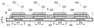
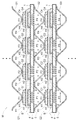
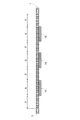
- FIG. 1 showing structure of electrochemical device, sectional view, and top view showing laminated structure Front view showing structure of electrochemical device, sectional view, and top view showing laminated structure Front view showing structure of electrochemical device, sectional view, and top view showing laminated structure Front view showing structure of electrochemical device, sectional view, and top view showing laminated structure Perspective view showing structure of electrochemical device Perspective view showing structure of electrochemical device
- FIG. 1 showing structure of electrochemical module
- FIG. 1 showing structure of electrochemical module
- FIG. 1 showing structure of electrochemical module Schematic diagram showing the configuration of the electrochemical device and energy system
- the electrochemical element Q includes a metal substrate 1 and a plurality of electrochemical reaction portions R.
- the metal substrate 1 has a gas flow permissible region P that allows gas flow between the front side 4 and the back side 5 of the metal substrate 1.
- the electrochemical reaction portion R has at least an electrode layer A, an electrolyte layer B, and a counter electrode layer C, and is disposed on the front side 4 of the metal substrate 1.
- the electrolyte layer B is disposed in a part between the electrode layer A and the counter electrode layer C, and the gas flowing through the gas flow allowable region P is supplied to the electrode layer A.
- five electrochemical reaction portions R are formed on the surface of the rectangular metal substrate 1 along the long side of the metal substrate 1.
- An electrochemical reaction part R3, a fourth electrochemical reaction part R4 and a fifth electrochemical reaction part R5) are arranged.
- the electrochemical reaction portion R is formed by forming three layers on the surface of the metal substrate 1.
- the first layer in contact with the metal substrate 1 includes an electrode layer A, an electrolyte layer B, and an insulating layer D.
- the second layer above the first layer includes an electrolyte layer B, an insulating layer D, and a conductive layer E.
- the counter electrode layer C is included in the upper third layer, that is, the uppermost third layer.
- FIG. 1 the upper part of FIG. 1 is a front view of the electrochemical element Q viewed from a direction perpendicular to the longitudinal direction.
- the middle part of FIG. 1 is a cross-sectional view of the electrochemical element Q viewed from the same direction as the upper part.
- the lower part of FIG. 1 is a top view of the electrochemical element Q as viewed from the front side 4 of the metal substrate 1.
- the longitudinal direction of the rectangular metal substrate 1 may be simply referred to as “longitudinal direction”, and the short direction of the rectangular metal substrate 1 may be simply referred to as “short direction”.
- the top view in the lower part of FIG. 1 shows a state in which a part of the first layer, the second layer, and the third layer is removed for explaining the layered structure of the electrochemical element Q.
- a line (thick line) indicating the position of each layer removal in the top view of the lower stage of FIG. 1 is shown in the front view of the upper stage of FIG.
- the upper third layer (counter electrode layer C) is removed from the center of the second electrochemical reaction portion R2 to the center of the third electrochemical reaction portion R3.
- the third layer and the second layer the electrolyte layer B, the insulating layer D, and the conductive layer E
- the metal substrate 1 is a metal rectangular flat plate.
- a plurality of through holes 2 are formed in the metal substrate 1 through the front side 4 and the back side 5. Gas can flow between the front side 4 and the back side 5 of the metal substrate 1 through the through hole 2.
- the plurality of through holes 2 are formed at intersections of lattices parallel to the long side and the short side of the metal substrate 1.
- the metal substrate 1 only needs to have sufficient strength to form an electrochemical element as a support, and is, for example, about 0.1 mm to 2 mm, preferably about 0.1 mm to 1 mm, more preferably about 0.1 mm. Those having a thickness of about 1 mm to 0.5 mm can be used.
- a sintered metal, a foam metal, etc. can also be used for the metal substrate 1.
- gas flow permissible areas P that are areas where the plurality of through holes 2 are gathered (first gas flow permissible area P1, second gas flow permissible).
- a region P2, a third gas flow allowable region P3, a fourth gas flow allowable region P4, and a fifth gas flow allowable region P5) are formed. That is, in this embodiment, the gas flow allowable region P is configured by the through hole 2.
- the five gas flow permissible regions P are formed apart from each other in the longitudinal direction. Between the gas flow permissible region P is a region (gas flow prohibition region) where gas flow is prohibited between the front side 4 and the back side 5 of the metal substrate 1.
- An insulating coating 3 (metal oxide coating) is formed on the surface of the metal substrate 1.
- the insulating coating 3 insulates between the electrode layer A of the electrochemical reaction part R and the metal substrate 1, thereby realizing insulation between the electrode layers A of the adjacent electrochemical reaction parts R. Therefore, the insulating coating 3 only needs to be formed on at least the front side of the metal substrate 1 and only needs to be formed in a region where the metal substrate 1 and the electrode layer A are in contact with each other.
- the insulating coating 3 is formed over the entire surface of the metal substrate 1.
- a conductive layer E is formed adjacent to the first electrochemical reaction portion R1 for electrical connection between the electrochemical element Q and the outside. It is preferable that the insulating film 3 is also formed in a region where the conductive layer E and the metal substrate 1 are in contact with each other.
- the insulation film 3 has a resistance value of about 1 k ⁇ ⁇ cm 2 or more, and if it is about 10 k ⁇ ⁇ cm 2 or more, a sufficient electromotive force and current amount can be secured even when the electrochemical element Q is operated as a fuel cell. This is preferable.
- the insulating coating 3 can be formed by various methods, a method of oxidizing the surface of the metal substrate 1 to form a metal oxide is preferably used.
- an alloy containing Cr is used as an SOFC inter-cell connection member
- an oxide film may be formed on the surface of the inter-cell connection member to suppress diffusion of Cr, thereby forming a diffusion prevention film.
- the diffusion prevention film is formed as thin as possible to reduce the resistance value.
- the insulating coating 3 of this embodiment insulates between the metal substrate 1 and the electrode layer A as described above, thereby insulating between the electrode layers A of the electrochemical reaction part R. In addition, the resistance value is increased.
- the insulating film 3 is common in that it is a metal oxide film, and therefore can also have a function as a diffusion prevention film (for example, suppression of Cr scattering).
- the insulating coating 3 is formed by applying a highly insulating oxide coating containing silica, alumina, 2-12 group element oxide, etc. on the surface of the metal substrate 1, PVD methods such as sputtering and PLD methods, CVD methods, spraying. It may be formed by a coating method or the like, or may be formed by plating and oxidation treatment.
- a metal material excellent in heat resistance, oxidation resistance and corrosion resistance is used.
- ferritic stainless steel, austenitic stainless steel, nickel base alloy or the like is used.
- an alloy containing chromium is preferably used.
- the thermal expansion coefficient is close to that of the material of the electrode layer A and the electrolyte layer B formed thereon, thereby improving reliability and durability. It is preferable because an excellent electrochemical device can be obtained.
- a Cr-rich Cr—Fe alloy containing 70% by weight or more of Cr can also be used.
- Ni—Cr—Al based alloys or Fe—Cr—Al based alloys can also be used.
- a material containing at least one of Si and Al is preferably used.
- the insulating film 3 having an appropriate resistance value can be suitably formed on the surface of the metal substrate 1 by heat-treating the metal substrate 1 in an air atmosphere or an atmosphere in which the oxygen partial pressure is controlled.
- the insulating coating 3 is easily formed on the surface by firing treatment. This is preferable.
- the insulating coating 3 can be more easily formed on the surface by firing treatment. It is more preferable because it is possible.
- the U-shaped member 11 and the lid portion 12 are joined to the metal substrate 1 to form the cylindrical gas circulation portion 10.
- the U-shaped member 11 is a member having a U-shaped cross section orthogonal to the longitudinal direction.
- the long side of the metal substrate 1 and the long side of the U-shaped member 11 (sides corresponding to the two vertices of the U-shape) are joined, and one end of the formed cylinder is closed by the lid 12. .
- circulation part 10 which has the internal space 22 inside and is flat as a whole, or flat rod shape is comprised.
- the metal substrate 1 is disposed in parallel to the central axis of the cylindrical gas circulation unit 10.
- the lid 12 has a plurality of holes (gas outlets 13). And the edge part on the opposite side to the cover part 12 of the cylindrical gas distribution part 10 is open
- the same material as that of the metal substrate 1 is used as the material of the U-shaped member 11 and the lid portion 12 because physical properties such as a thermal expansion coefficient are unified in the entire tubular gas circulation portion 10.
- YSZ yttrium stabilized zirconia
- GDC gadolin-doped
- the thermal expansion coefficient is close. Therefore, even when the low temperature and high temperature cycle are repeated, the electrochemical element Q is hardly damaged. Therefore, the electrochemical element Q having excellent long-term durability can be realized, which is preferable.
- the material of the tubular gas flow portion 10 it is preferable to use a material thermal conductivity greater than 3Wm -1 K -1, more preferably as long as the material above the 10Wm -1 K -1.
- stainless steel has a thermal conductivity of about 15 to 30 Wm ⁇ 1 K ⁇ 1 , and is therefore suitable as a material for the cylindrical gas circulation part 10.
- the material of the tubular gas circulation part 10 is a high toughness material that does not cause brittle fracture.
- a metal material has high toughness compared to a ceramic material or the like, and is suitable as a material for the cylindrical gas circulation part 10.
- the portions other than the gas flow allowable region P of the metal substrate 1 are configured so that gas cannot flow outward from the internal space 22 of the cylindrical gas circulation part 10. Therefore, it is preferable that the portion of the cylindrical gas circulation part 10 excluding the gas flow allowable region P is formed of a material that does not transmit gas, such as crystalline metal.
- the gas flow permissible region P of the metal substrate 1 can be formed of a porous metal plate or the like instead of the through hole 2 described above.
- the electrochemical reaction part R includes an electrode layer A, an electrolyte layer B, a counter electrode layer C, and an intermediate layer.
- the electrode layer A is formed in a film state on the surface 4 of the metal substrate 1, that is, on the insulating coating 3.
- the film thickness can be, for example, about 1 ⁇ m to 100 ⁇ m, preferably about 5 ⁇ m to 50 ⁇ m. By using such a film thickness, it is possible to secure sufficient electrode performance while reducing the cost by reducing the amount of expensive electrode layer material used.
- the material of the electrode layer A include NiO-cerium oxide (ceria) as a main component, Ni-cerium oxide (ceria) as a main component, NiO-zirconia as a main component, Ni-zirconia.
- a composite material such as a material mainly containing CuO-cerium oxide (ceria) or a material mainly containing Cu-cerium oxide (ceria) can be used.
- cerium oxide (ceria), zirconia, or the like or a solid solution doped with a different element is referred to as a composite aggregate.
- the electrode layer A is formed so as to have gas permeability.
- the electrode layer A is configured to have a plurality of fine pores on the surface and inside.
- the electrode layer A is a low temperature baking method (for example, a wet method using a baking process in a low temperature region of about 1100 ° C. or less without performing a baking process in a high temperature region such as 1400 ° C.), a sputtering method, or a pulse laser deposition. It is preferably formed by a PVD method such as a method, a CVD method, a spray coating method or the like. By these processes that can be used in a low temperature range, a good electrode layer A can be obtained by a treatment in a low temperature range of, for example, about 1100 ° C. or less, without using baking in a high temperature range such as 1400 ° C., for example.
- a low temperature baking method for example, a wet method using a baking process in a low temperature region of about 1100 ° C. or less without performing a baking process in a high temperature region such as 1400 ° C.
- the element Q is preferable because it can be realized.
- the electrolyte layer B is provided as a film between the electrode layer A and the counter electrode layer C.
- the film thickness can be, for example, about 1 ⁇ m to 50 ⁇ m, preferably about 1 ⁇ m to 20 ⁇ m, more preferably about 2 ⁇ m to 10 ⁇ m. By using such a film thickness, it is possible to ensure sufficient electrolyte performance while reducing the amount of expensive electrolyte layer material used and reducing costs.
- the material of the electrolyte layer B solid electrolyte materials capable of conducting oxide ions and hydrogen ions, such as various zirconia materials, cerium oxide materials, and various perovskite complex oxides, can be used. In particular, zirconia ceramics are preferably used.
- the electrolyte layer B is made of zirconia-based ceramics, the temperature during operation of the electrochemical element Q can be made higher than that of ceria-based ceramics, and an extremely efficient electrochemical element Q can be configured.
- the electrolyte layer B is formed by a low-temperature baking method (for example, a wet method using a baking process in a low temperature range of about 1100 ° C. or less without performing a baking process in a high temperature range such as 1400 ° C.), a sputtering method, or a pulse laser deposition. It is preferably formed by a PVD method such as a method, a CVD method, a spray coating method or the like.
- a low-temperature baking method for example, a wet method using a baking process in a low temperature range of about 1100 ° C. or less without performing a baking process in a high temperature range such as 1400 ° C.
- the element Q is preferable because it can be realized.
- Electrolyte layer B is densely configured to maintain hermeticity.
- the electrolyte layer B preferably includes a layer having a relative density of 90% or more. Further, it is more preferable that a layer having a relative density of 95% or more is included, and it is more preferable that a layer having a relative density of 98% or more is included.
- the electrolyte layer B can be made dense by increasing the relative density.
- the relative density represents the ratio of the density of the electrolyte layer B actually formed to the theoretical density of the electrolyte material.
- the counter electrode layer C is provided as a film on the electrolyte layer B.
- the film thickness can be, for example, about 1 ⁇ m to 100 ⁇ m, preferably about 5 ⁇ m to 50 ⁇ m. By using such a film thickness, it is possible to secure sufficient counter electrode performance while reducing the amount of expensive counter electrode layer material used and reducing costs.
- the material of the counter electrode layer C include LSCF (La—Sr—Co—Fe based oxide), LSC (La—Sr—Co based oxide), LSM (La—Sr—Mn based oxide), and SSC.
- Composite oxides such as (Sm—Sr—Co-based oxide) and SDC (Ce—Sm-based oxide) can be used.
- the counter electrode layer C is formed by a low temperature baking method (for example, a wet method using a baking process in a low temperature range of about 1100 ° C. or less without performing a baking process in a high temperature range such as 1400 ° C.), a sputtering method, or a pulse laser device. It is preferably formed by PVD method such as position method, CVD method, spray coating method or the like. By these processes that can be used in a low temperature range, a good counter electrode layer C can be obtained by a treatment in a low temperature range of about 1100 ° C. or less, for example, without using baking in a high temperature range such as 1400 ° C.
- a low temperature baking method for example, a wet method using a baking process in a low temperature range of about 1100 ° C. or less without performing a baking process in a high temperature range such as 1400 ° C.
- the element Q is preferable because it can be realized.
- An intermediate layer may be formed between the electrode layer A and the electrolyte layer B in the form of a film.
- the film thickness can be, for example, about 1 ⁇ m to 100 ⁇ m, preferably about 2 ⁇ m to 50 ⁇ m, more preferably about 5 ⁇ m to 20 ⁇ m. With such a film thickness, it is possible to secure sufficient intermediate layer performance while reducing the cost by reducing the amount of expensive intermediate layer material used.
- As the material for the intermediate layer for example, a cerium oxide-based material, a zirconia-based material, or the like can be used.
- the intermediate layer is formed by a low temperature baking method (for example, a wet method using a baking process in a low temperature region of about 1100 ° C. or less without performing a baking process in a high temperature region such as 1400 ° C.), a sputtering method, or a pulse laser deposition method. It is preferable to form by PVD method such as CVD method, spray coating method or the like. By these processes that can be used in a low temperature range, a good intermediate layer can be obtained by a treatment in a low temperature range of about 1100 ° C. or less, without using baking in a high temperature range of 1400 ° C. or the like.
- a low temperature baking method for example, a wet method using a baking process in a low temperature region of about 1100 ° C. or less without performing a baking process in a high temperature region such as 1400 ° C.
- PVD method such as CVD method, spray coating method or the like.
- the element Q is preferable because it can be realized.
- an intermediate layer may be formed in a film state between the electrolyte layer B and the counter electrode layer C.
- the film thickness can be, for example, about 1 ⁇ m to 100 ⁇ m, preferably about 2 ⁇ m to 50 ⁇ m, more preferably about 5 ⁇ m to 20 ⁇ m. With such a film thickness, it is possible to secure sufficient intermediate layer performance while reducing the cost by reducing the amount of expensive intermediate layer material used.
- a cerium oxide-based material, a zirconia-based material, or the like can be used as the material for the intermediate layer.
- the intermediate layer is formed by a low temperature baking method (for example, a wet method using a baking process in a low temperature region of about 1100 ° C. or less without performing a baking process in a high temperature region such as 1400 ° C.), a sputtering method, or a pulse laser deposition method. It is preferable to form by PVD method such as CVD method, spray coating method or the like.
- a good intermediate layer can be obtained by a treatment in a low temperature range of about 1100 ° C. or less, without using baking in a high temperature range of 1400 ° C. or the like. Therefore, it is possible to suppress the metal substrate 1 from being damaged due to high temperature heating, and it is possible to suppress elemental interdiffusion between the metal substrate 1 and the electrode layer A due to high temperature heating, which is excellent in durability.
- the element Q is preferable because it can be realized.
- One or both of the intermediate layers described above can be provided. That is, a configuration in which the electrode layer A, the electrolyte layer B, the intermediate layer, and the counter electrode layer C are laminated in this order is also possible. A configuration in which the electrode layer A, the intermediate layer, the electrolyte layer B, and the counter electrode layer C are laminated in this order is also possible. A configuration in which the electrode layer A, the intermediate layer, the electrolyte layer B, the intermediate layer, and the counter electrode layer C are laminated in this order is also possible.
- the electrochemical reaction section R configured as described above receives gas supply and causes an electrochemical reaction.
- the electrochemical reaction unit R operates as a fuel cell
- an oxide ion conductor for example, a fuel containing hydrogen gas is supplied to the electrode layer A, and a gas containing oxygen is supplied to the counter electrode layer C. Is supplied.
- oxygen molecules O 2 react with electrons e ⁇ to generate oxygen ions (oxide ions) O 2 ⁇ .
- the oxygen ions O 2 ⁇ move through the electrolyte layer B to the electrode layer A.
- the hydrogen molecule H 2 reacts with the oxygen ions O 2 ⁇ to generate water H 2 O and electrons e ⁇ .
- the electrochemical reaction part R operates as an electrolytic cell
- an oxide ion conductor when used as the electrolyte, when a voltage is applied between the electrode layer A and the counter electrode layer C, the electrode layer A
- the water molecule H 2 O receives the electrons e ⁇ and generates hydrogen molecules H 2 and oxygen ions (oxide ions) O 2 ⁇ .
- Oxygen ions O 2 ⁇ move through the electrolyte layer B to the counter electrode layer C.
- oxygen ions O 2 ⁇ emit electrons and become oxygen molecules O 2 .
- the electrode layer A, the electrolyte layer B, and the counter electrode layer C of the first electrochemical reaction unit R1 are referred to as a first electrode layer A1, a first electrolyte layer B1, and a first counter electrode layer C1.
- the electrode layer A, the electrolyte layer B, and the counter electrode layer C of the second electrochemical reaction unit R2 are referred to as a second electrode layer A2, a second electrolyte layer B2, and a second counter electrode layer C2.
- a plurality of electrochemical reaction portions R are electrically connected in series. And the electrode layer A of one electrochemical reaction part R and the counter electrode layer C of the other electrochemical reaction part R are electrically connected.
- first electrochemical reaction unit R1 and the second electrochemical reaction unit R2 will be described based on the middle cross-sectional view of FIG.
- an insulating layer D and a conductive layer E are formed between the first electrochemical reaction part R1 and the second electrochemical reaction part R2.
- a series connection between the first electrochemical reaction part R1 and the second electrochemical reaction part R2 is realized.
- the insulating layer D can be made of an insulating metal oxide such as alumina.
- the insulating layer D is densely formed and is formed in a gas tight state in which gas permeability is suppressed.
- the conductive layer E is also called an interconnector, but can be made of a conductive metal oxide such as LaCrO 3 (lanthanum chromite) or SrTiO 3 (strontium titanate).
- the conductive layer E is densely formed and is formed in a gas tight state in which gas permeability is suppressed.
- an insulating layer D is formed between the first electrode layer A1 and the second electrode layer A2.
- an insulating layer D and a conductive layer E are formed between the first electrolyte layer B1 and the second electrolyte layer B2.
- the second insulating layer D is formed across both the first insulating layer and the first electrode layer A1.
- the conductive layer E is formed across both the first insulating layer and the second electrode layer A2.
- the first counter electrode layer C1 is formed from above the first electrolyte layer B1 over the insulating layer D of the second layer to the conductive layer E. That is, the second conductive layer E is in contact with and electrically connected to both the first counter electrode layer C1 and the second electrode layer A2.
- the first electrode layer A1 and the second electrode layer A2 are insulated by the presence of the insulating layer D.
- the first counter electrode layer C1 and the second electrode layer A2 are electrically connected by the presence of the conductive layer E.
- the electrochemical reaction part R When the electrochemical reaction part R operates as a fuel cell, an electromotive force is generated between the electrode layer A and the counter electrode layer C as described above. Then, since the first counter electrode layer C1 and the second electrode layer A2 are electrically connected, the electromotive force of the first electrochemical reaction unit R1 and the electromotive force of the second electrochemical reaction unit R2 are added. The combined electromotive force is generated between the first electrode layer A1 and the second counter electrode layer C2. That is, in this case, it can be said that the first electrochemical reaction part R1 and the second electrochemical reaction part R2 are electrically connected in series.
- each electrochemical reaction part R from the second electrochemical reaction part R2 to the fifth electrochemical reaction part R5 is also electrically connected in series.
- the structure for electrically connecting with the exterior of the electrochemical element Q is arrange
- the current collecting member 26 is connected to the fifth counter electrode layer C5 of the fifth electrochemical reaction unit R5.
- the conductive layer E is connected to the first electrode layer A1 of the first electrochemical reaction unit R1, and the current collecting member 26 is connected to the conductive layer E.
- a member having conductivity and gas permeability is used as the current collecting member 26 .
- an expanded metal, a metal mesh, or a felt-like member using a metal foil with an oxidation resistant coating is used as the current collecting member 26 .
- the electrochemical element Q In the electrochemical element Q, the gas flowing through the gas flow allowable region P of the metal substrate 1 is supplied to the electrode layer A, but it is necessary to suppress the leakage of the gas to the counter electrode layer C side. . Therefore, the electrochemical element Q according to the present embodiment has the following structure for sealing a gas.
- the first electrode layer A1 is formed to cover the first gas flow allowable region P1.
- the other second electrode layer A2 to fifth electrode layer A5 are formed so as to cover the second gas flow allowable region P2 to the fifth gas flow allowable region P5, respectively. That is, the electrode layer A is provided in a region larger than the gas flow allowable region P so as to cover the gas flow allowable region P. In this case, if the electrode layer A is covered with a gas tight layer, gas leakage can be suppressed.
- the third electrode layer A3 is covered with a third electrolyte layer B3, an insulating layer D, and a conductive layer E.
- the third electrolyte layer B3 is disposed so as to cover at least the third electrode layer A3 provided in the third gas flow allowable region P3.
- the third electrolyte layer B3 is formed over a wider width than the third electrode layer A3 in the short direction.
- the third electrode layer A3 is disposed on the third electrode layer A3, that is, on the second layer in the region where the third electrode layer A3 exists.
- the third electrolyte layer B3 is disposed on the metal substrate 1, that is, the first layer.
- the third electrolyte layer B3 of the first layer and the third electrolyte layer B3 of the second layer are formed as a continuous layer, and gas leakage from the connection site between them is suppressed.
- Both ends in the longitudinal direction of the third electrode layer A3 are covered with an insulating layer D and a conductive layer E.
- the insulating layer D and the conductive layer E of the second layer are elongated in the short direction, and in the region where the third electrode layer A3 does not exist (regions on both sides of the third electrode layer A3 in the short direction), the first layer Are connected to the insulating layer D and the conductive layer E, respectively.
- the first layer insulating layer D and the second layer insulating layer D, and the first layer conductive layer E and the second layer conductive layer E are formed as continuous layers. Gas leakage is suppressed.
- the third electrode layer A3 is covered with the third electrolyte layer B3, the insulating layer D, and the conductive layer E. Since all of the electrolyte layer B, the insulating layer D, and the conductive layer E are gas tight layers with low gas permeability, the gas supplied to the third electrode layer A3 leaks to the counter electrode layer C side by the above configuration. It is suppressed from taking out.
- the structure of the electrochemical reaction part R according to this embodiment described above can be formed as follows. First, the first electrode layer A, the insulating layer D, and the conductive layer E are formed on the metal substrate 1 in the planar shape shown in the top view in the lower part of FIG. Next, the second electrolyte layer B, the insulating layer D, and the conductive layer E are formed in the planar shape shown in the top view of the lower stage of FIG. 1, that is, with a wider width in the short direction than the first layer. And on the first layer. As a result, the electrode layer A is covered with the electrolyte layer B, the insulating layer D, and the conductive layer E. Then, the third counter electrode layer C is formed on the second layer.
- FIG. 1 An electrochemical element Q according to the second embodiment is shown in FIG.
- the same components as those in the first embodiment are denoted by the same reference numerals, and description thereof may be omitted.
- the through hole 2 is continuously formed along the longitudinal direction of the metal substrate 1. That is, the gas flow allowable area P is formed as a continuous area. Also in this embodiment, the electrode layer A provided in the gas flow allowable region P is covered with the electrolyte layer B, the insulating layer D, and the conductive layer E. Therefore, the gas supplied to the electrode layer A is suppressed from leaking to the counter electrode layer C side.
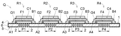
- FIG. 1 An electrochemical element Q according to the third embodiment is shown in FIG.
- the electrode layer A of one electrochemical reaction part R and the electrode layer A of another electrochemical reaction part R are electrically connected, and thus a plurality of electrochemical reaction parts R are electrically parallel. It is connected to the.
- a diffusion prevention film 6 (metal oxide film) is formed on at least a portion of the surface of the metal substrate 1 in contact with the electrode layer A instead of the insulating film.
- the diffusion prevention film 6 is provided to suppress scattering of Cr from the metal substrate 1.
- the diffusion prevention film 6 has conductivity and is configured to have a low resistance value so as not to suppress conduction between the electrode layer A of the electrochemical reaction portion R and the metal substrate 1.
- the metal oxide film covering the region of the surface of the metal substrate 1 that is not covered by either the electrode layer, the electrolyte layer, or the counter electrode layer suppresses evaporation of components such as Cr oxide from the metal substrate 1. It may be an insulating film or a conductive diffusion prevention film.
- the electromotive force and the amount of current can be secured, which is preferable.
- a metal material excellent in heat resistance, oxidation resistance and corrosion resistance is used.
- ferritic stainless steel, austenitic stainless steel, nickel base alloy or the like is used.
- an alloy containing chromium is preferably used.
- the thermal expansion coefficient is close to that of the material of the electrode layer A and the electrolyte layer B formed thereon, thereby improving reliability and durability. It is preferable because an excellent electrochemical device can be obtained.
- a Cr-rich Cr—Fe alloy containing 70% by weight or more of Cr can also be used.
- Ni—Cr—Al based alloys or Fe—Cr—Al based alloys can also be used.
- the diffusion preventing film 6 can be formed by various methods, a method of oxidizing the surface of the metal substrate 1 to form a metal oxide is preferably used. In that case, the diffusion prevention film 6 having an appropriate thickness and resistance value is formed on the metal substrate 1 by heat-treating the metal substrate 1 in an atmosphere in which the oxygen partial pressure is controlled low, or in an inert gas or hydrogen atmosphere. It can be suitably formed on the surface.
- an Fe—Cr alloy material containing about 15% to 25% by weight of Cr is used for the metal substrate 1, a diffusion prevention film containing chromium oxide as a main component is easily formed on the surface by firing treatment.
- the diffusion prevention film 6 may be formed on the surface of the metal substrate 1 by a PVD method such as a sputtering method or a PLD method, a CVD method, a spray coating method, or the like, or may be formed by plating and oxidation treatment. . Further, the diffusion preventing film 6 may include a spinel phase having high conductivity.
- five gas flow allowable regions P are formed on the metal substrate 1 so as to be separated from each other.
- Five electrochemical reaction parts R are formed to be separated from each other.
- first, five electrode layers A are formed in areas larger than the respective gas flow allowable areas P so as to cover the gas flow allowable areas P. Yes.
- the five electrode layers A are formed apart from each other.
- Five electrolyte layers B are formed in a region larger than each electrode layer A so as to cover each electrode layer A.
- the five electrolyte layers B are formed apart from each other.
- Five counter electrode layers C are formed on each electrolyte layer B.
- Each gas flow allowable region P is covered with the electrode layer A, and each electrode layer A is covered with the electrolyte layer B, so that the gas supplied from the gas flow allowable region P to the electrode layer A is counter electrode layer. Leakage to the C side is suppressed. That is, in this embodiment, the metal substrate 1 has a plurality of gas flow permissible regions P that are separated from each other, and the electrolyte layer B of the electrochemical reaction part R is provided in each gas flow permissible region P. Further, the electrode layer A is disposed over the electrode layer A.
- the diffusion preventing film 6 having conductivity is formed on the surface of the metal substrate 1. Accordingly, the plurality of electrode layers A that are formed apart from each other are electrically connected through the metal substrate 1.
- the electrode layer A and the counter electrode layer C of the adjacent electrochemical reaction part R were electrically connected, and the electrochemical reaction part R was connected in series.
- the electrode layer A of the adjacent electrochemical reaction part R is electrically connected, so that the plurality of electrochemical reaction parts R are electrically connected in parallel.
- the electrochemical device Q When the electrochemical device Q according to this embodiment is operated as a fuel cell, hydrogen that has flowed through the gas flow allowable region P is supplied to the electrode layer A, oxygen is supplied to the counter electrode layer C, and the electrode layer A and An electromotive force is generated between the counter electrode layer C and the counter electrode layer C. Since the first electrode layer A1 to the fifth electrode layer A5 are electrically connected by the metal substrate 1, they have the same potential. Then, a current collecting member (not shown) attached to the first counter electrode layer C1 to the fifth counter electrode layer C5 and the metal substrate 1 (or the cylindrical gas flow part 10) are connected to the outside, and an electromotive force is generated outside. ⁇ Current is taken out. That is, five fuel cells (electrochemical reaction unit R) connected in parallel supply power to the outside.
- the electrochemical device Q When the electrochemical device Q according to this embodiment is operated as an electrolytic cell, water (water vapor) that has flowed through the gas flow allowable region P is supplied to the electrode layer A, and the first counter electrode layer C1 to the fifth counter electrode A voltage is applied between the current collecting member (not shown) attached to the layer C5 and the metal substrate 1 (or the tubular gas circulation part 10). Then, since the first electrode layer A1 to the fifth electrode layer A5 are electrically connected by the metal substrate 1, a voltage is applied to each electrochemical reaction portion R, and the electrolytic reaction proceeds. That is, also in this case, it can be considered that five electrolysis cells are connected in parallel and operate, and it can be said that the electrochemical reaction part R is electrically connected in parallel.
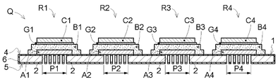
- FIG. 4 shows an electrochemical element Q according to the fourth embodiment.
- the through hole 2 is continuously formed along the longitudinal direction of the metal substrate 1 as in the second embodiment. That is, the gas flow allowable area P is formed as a continuous area.
- a diffusion prevention film 6 is formed on the surface of the metal substrate 1.
- first electrode layer A1 to fifth electrode layer A5 are formed on the front side 4 of the metal substrate 1.
- the five electrode layers A are formed apart from each other.
- the electrolyte layer B is formed in a region larger than the gas flow allowable region P so as to cover the gas flow allowable region P.
- the electrolyte layer B is formed as a continuous layer over the first layer and the second layer, and almost on the entire front side 4 of the metal substrate 1.
- the five electrode layers A are covered with the electrolyte layer B. Thereby, it is suppressed that the gas supplied to the electrode layer A leaks out to the counter electrode layer C side.
- Five counter electrode layers C are formed in a region corresponding to the electrode layer A on the electrolyte layer B.
- the first electrochemical reaction portion R1 is formed by the first electrode layer A1, the first counter electrode layer C1, and the first electrolyte layer B1 that is sandwiched between them.
- the second electrode layer A2 to the fifth electrode layer A5 the second counter electrode layer C2 to the fifth counter electrode layer C5, and the second electrolyte layer B2 to the fifth electrolyte layer B5 that are sandwiched therebetween.
- the second electrochemical reaction part R2 to the fifth electrochemical reaction part R5 are formed. That is, in this embodiment, a plurality of electrochemical reaction parts R are arranged on the front side 4 of the metal substrate 1.
- the plurality of electrode layers A formed separately from each other are electrically connected through the metal substrate 1. Therefore, it can be said that the plurality of electrochemical reaction portions R are electrically connected in parallel.
- the plurality of electrochemical reaction portions R are provided in one row along the longitudinal direction of the rectangular metal substrate 1. It is possible to modify this and form a plurality of electrochemical reaction portions R in a plurality of rows.
- FIG. 5 shows an electrochemical element Q according to the fifth embodiment.
- an example in which five electrochemical reaction portions R are arranged in two rows on the metal substrate 1 is shown.
- the current collecting member 26, the conductive layer E, the first electrochemical reaction portion R1, and the second electrochemical reaction portion R2 are arranged in this order in the front row in FIG. 5, and the rear row in FIG.
- the fifth electrochemical reaction part R5, the fourth electrochemical reaction part R4, and the third electrochemical reaction part R3 are arranged in this order.
- An insulating coating 3 (metal oxide coating) is formed on the surface of the metal substrate 1.
- the metal substrate 1 is formed with a plurality of through holes 2 that penetrate the front side 4 and the back side 5, and the plurality of through holes 2 are located at positions corresponding to the five electrochemical reaction portions R.
- Five gas flow permissible areas P which are areas where the gas flows, are formed.
- the gas flow allowable region P can be formed over the entire metal substrate 1. However, in that case, the gas flow allowable region P is formed so as to be inside the region where the conductive layer E and the electrolyte layer B are formed, and the gas from the back side 5 of the metal substrate 1 is on the side of the counter electrode layer C. It is necessary to suppress leakage to (the front side 4 of the metal substrate 1).
- FIG. 5 shows the metal substrate 1 and the electrochemical reaction part R, as in the first embodiment, a U-shaped member 11 and a lid part 12 are attached to the metal substrate 1 to form a cylindrical gas flow part. 10 can also be formed.
- the first electrochemical reaction unit R1 to the fifth electrochemical reaction unit R5 are electrically connected in series and connected to the pair of current collecting members 26.
- the electrode layer A of one electrochemical reaction part R and the counter electrode layer C of another electrochemical reaction part R are electrically connected.
- the structure of each electrochemical reaction portion R that is, the arrangement and positional relationship of the electrode layer A, the electrolyte layer B, the counter electrode layer C, the insulating layer D, and the conductive layer E are formed in the same manner as in the first embodiment.
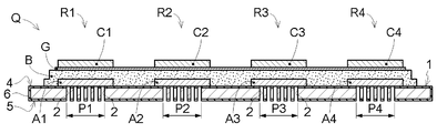
- electrochemical reaction portions R are arranged in two rows on the metal substrate 1 .
- the first electrochemical reaction unit R1 and the second electrochemical reaction unit R2 are arranged in this order in the front row in FIG. 6, and the fourth electrochemical reaction unit R4 and the second electrochemical reaction unit R4 in the rear row in FIG.
- the third electrochemical reaction portion R3 is arranged in this order.
- a diffusion prevention film 6 (metal oxide film) is formed on the surface of the metal substrate 1.
- the metal substrate 1 has a plurality of through holes 2 formed through the front side 4 and the back side 5, and a plurality of through holes are provided at positions corresponding to the four electrochemical reaction portions R.
- Four gas flow permissible areas P which are areas where 2 gathers, are formed.
- the gas flow allowable region P can be formed over the entire metal substrate 1.
- the gas flow allowable region P is formed so as to be inside the region where the conductive layer E and the electrolyte layer B are formed, and the gas from the back side 5 of the metal substrate 1 is on the side of the counter electrode layer C. It is necessary to suppress leakage to (the front side 4 of the metal substrate 1).
- the first electrochemical reaction unit R1 to the fourth electrochemical reaction unit R4 are electrically connected in parallel. That is, the electrode layer A of one electrochemical reaction part R and the electrode layer A of another electrochemical reaction part R are electrically connected.
- the structure of each electrochemical reaction portion R that is, the arrangement and positional relationship of the electrode layer A, the electrolyte layer B, and the counter electrode layer C are formed as in the fourth embodiment.
- FIG. 6 shows the metal substrate 1 and the electrochemical reaction portion R, as in the first embodiment, a U-shaped member 11 and a lid portion 12 are attached to the metal substrate 1 to form a cylindrical gas flow portion. 10 can also be formed.
- the electrochemical module M is a module arranged in a state where a plurality of the above-described electrochemical elements Q are stacked.
- the electrochemical module M according to the seventh embodiment includes an electrochemical element Q in which a plurality of electrochemical reaction units R are electrically connected in series, that is, the first embodiment, the second embodiment, and the fifth embodiment.
- the electrochemical element Q according to the above is used.
- the electrochemical module M has a gas manifold 17 and five electrochemical elements Q.
- the electrochemical element Q is connected to the gas manifold 17 so that the gas inlet 21 of the tubular gas circulation part 10 of the electrochemical element Q communicates with the internal space of the gas manifold 17.
- five electrochemical elements Q are stacked in such a posture that the electrochemical reaction portion R faces one side (the right side in FIG. 7) and is attached to the gas manifold 17.
- the space between the electrochemical reaction portion R and the metal substrate 1, that is, the tubular gas circulation portion 10 is between Insulated. Therefore, since it is not necessary to insulate the cylindrical gas flow part 10 to the gas manifold 17, it can be attached by a simple and strong method such as welding.
- the electrochemical elements Q of the electrochemical module M are electrically connected to each other.
- the current collecting members 26 connected to the first electrochemical reaction portion R1 of each electrochemical element Q are electrically connected to each other and connected to the outside.
- the current collection member 26 connected to 5th electrochemical reaction part R5 of each electrochemical element Q is mutually connected electrically, and is connected with the exterior.
- FIG. 8 shows another embodiment of the electrochemical module M.
- the electrochemical module M according to the eighth embodiment includes an electrochemical element Q in which a plurality of electrochemical reaction units R are electrically connected in parallel, that is, the third embodiment, the fourth embodiment, and the sixth embodiment.
- the electrochemical element Q according to the above is used.
- the electrochemical element Q is connected to the gas manifold 17 so that the gas inlet 21 of the tubular gas circulation part 10 of the electrochemical element Q communicates with the internal space of the gas manifold 17.
- five electrochemical elements Q are stacked in such a posture that the electrochemical reaction portion R faces one side (the right side in FIG. 7) and is attached to the gas manifold 17.
- the current collection member 26 is arrange
- the cylindrical gas circulation part 10 when an electrochemical element Q in which a plurality of electrochemical reaction portions R are electrically connected in parallel is used, between the electrochemical reaction portion R and the metal substrate 1, that is, the cylindrical gas flow portion 10. Is not insulated and is in a conducting state. Therefore, when the cylindrical gas circulation part 10 is attached to the gas manifold 17, it is necessary to insulate between the cylindrical gas circulation part 10 and the gas manifold 17. For example, the cylindrical gas circulation part 10 and the gas manifold 17 are joined by a glass sealing material.
- FIG. 9 shows another embodiment of the electrochemical module M.
- the electrochemical module M according to the ninth embodiment includes an electrochemical element Q according to the sixth embodiment shown in FIG. 6, that is, an electrochemical element in which a plurality of electrochemical reaction units R are electrically connected in parallel. Q can be preferably used.
- the electrochemical module M is configured by laminating the electrochemical element Q with the inter-cell connection member 71 interposed therebetween.
- the inter-cell connection member 71 is a plate-like member that has conductivity and does not have gas permeability, and grooves 72 that are orthogonal to each other are formed on the front surface and the back surface.
- the inter-cell connection member 71 can be made of metal such as stainless steel or metal oxide.
- one groove 72 becomes the first gas flow path 72a, and supplies gas to the front side of the electrochemical element Q, that is, the counter electrode layer C.
- the other groove 72 becomes the second gas flow path 72b, and supplies gas to the back side of the electrochemical element Q, that is, the gas flow allowable region P of the metal substrate 1.
- this electrochemical module M When operating this electrochemical module M as a fuel cell, oxygen is supplied to the first gas channel 72a and hydrogen is supplied to the second gas channel 72b. If it does so, reaction as a fuel cell will progress in each electrochemical reaction part R of electrochemical element Q, and electromotive force and current will be generated. The generated electric power is taken out of the electrochemical module M from the inter-cell connection members 71 at both ends of the stacked electrochemical element Q.
- the grooves 72 orthogonal to each other are formed on the front and back surfaces of the inter-cell connection member 71.
- the grooves 72 parallel to each other are formed on the front and back surfaces of the inter-cell connection member 71. You can also.
- the electrochemical device Y and the energy system Z can be constructed using the electrochemical element Q and the electrochemical module M described above.
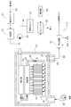
- FIG. 10 shows an outline of the energy system Z and the electrochemical device Y.
- the energy system Z includes an electrochemical device Y and a heat exchanger 53 as an exhaust heat utilization unit that reuses the heat discharged from the electrochemical device Y.
- the electrochemical device Y includes an electrochemical module M, a desulfurizer 31 and a reformer 34, a fuel supply unit that supplies a fuel gas containing a reducing component to the electrochemical module M, and an electrochemical module. And an inverter 38 for extracting electric power from M.
- the electrochemical device Y includes a desulfurizer 31, a reforming water tank 32, a vaporizer 33, a reformer 34, a blower 35, a combustion unit 36, an inverter 38, a control unit 39, a storage container 40, and an electrochemical module M.
- a desulfurizer 31 a reforming water tank 32, a vaporizer 33, a reformer 34, a blower 35, a combustion unit 36, an inverter 38, a control unit 39, a storage container 40, and an electrochemical module M.
- the desulfurizer 31 removes (desulfurizes) sulfur compound components contained in hydrocarbon-based raw fuel such as city gas.
- hydrocarbon-based raw fuel such as city gas.
- the vaporizer 33 generates steam from the reformed water supplied from the reformed water tank 32.
- the reformer 34 steam-reforms the raw fuel desulfurized by the desulfurizer 31 using the steam generated by the vaporizer 33 to generate a reformed gas containing hydrogen.
- the electrochemical module M uses the reformed gas supplied from the reformer 34 and the air supplied from the blower 35 to generate an electrochemical reaction to generate power.
- the combustion unit 36 mixes the reaction exhaust gas discharged from the electrochemical module M and air, and combusts the combustible component in the reaction exhaust gas.
- the electrochemical module M has a plurality of electrochemical elements Q and a gas manifold 17.
- the plurality of electrochemical elements Q are arranged in parallel while being electrically connected to each other, and one end (lower end) of the electrochemical element Q is fixed to the gas manifold 17.
- the electrochemical element Q generates electricity by causing an electrochemical reaction between the reformed gas supplied through the gas manifold 17 and the air supplied from the blower 35.
- the inverter 38 adjusts the output power of the electrochemical module M to the same voltage and the same frequency as the power received from the commercial system (not shown).
- the control unit 39 controls the operation of the electrochemical device Y and the energy system Z.
- the vaporizer 33, the reformer 34, the electrochemical module M, and the combustion unit 36 are stored in the storage container 40.
- the reformer 34 performs the reforming process of the raw fuel using the combustion heat generated by the combustion of the reaction exhaust gas in the combustion unit 36.
- the raw fuel is supplied to the desulfurizer 31 through the raw fuel supply path 42 by the operation of the booster pump 41.
- the reforming water in the reforming water tank 32 is supplied to the vaporizer 33 through the reforming water supply path 44 by the operation of the reforming water pump 43.
- the raw fuel supply path 42 is downstream of the desulfurizer 31 and is joined to the reformed water supply path 44, and the reformed water and raw fuel merged outside the storage container 40 are stored in the storage container.
- the carburetor 33 provided in 40 is supplied.
- the reformed water is vaporized by the vaporizer 33 and becomes steam.
- the raw fuel containing the steam generated in the vaporizer 33 is supplied to the reformer 34 through the steam-containing raw fuel supply path 45.
- the raw fuel is steam-reformed by the reformer 34, and a reformed gas (first gas having a reducing component) containing hydrogen gas as a main component is generated.
- the reformed gas generated in the reformer 34 is supplied to the gas manifold 17 of the electrochemical module M through the reformed gas supply path 46.
- the reformed gas supplied to the gas manifold 17 is distributed to the plurality of electrochemical elements Q and supplied to the electrochemical element Q from the lower end, which is a connection portion between the electrochemical elements Q and the gas manifold 17.
- Hydrogen (reducing component) in the reformed gas is mainly used for electrochemical reaction in the electrochemical element Q.
- the reaction exhaust gas containing the remaining hydrogen gas that has not been used for the reaction is discharged from the upper end of the electrochemical element Q to the combustion unit 36.
- the reaction exhaust gas is combusted in the combustion part 36 and is discharged as combustion exhaust gas from the combustion exhaust gas outlet 50 to the outside of the storage container 40.
- a combustion catalyst portion 51 (for example, a platinum-based catalyst) is disposed at the combustion exhaust gas outlet 50 to burn and remove reducing components such as carbon monoxide and hydrogen contained in the combustion exhaust gas.
- the combustion exhaust gas discharged from the combustion exhaust gas outlet 50 is sent to the heat exchanger 53 through the combustion exhaust gas discharge passage 52.
- the heat exchanger 53 exchanges heat between the flue gas generated by the combustion in the combustion unit 36 and the supplied cold water to generate hot water. That is, the heat exchanger 53 operates as an exhaust heat utilization unit that reuses the heat exhausted from the electrochemical device Y.
- reaction exhaust gas utilization part which utilizes the reaction exhaust gas discharged
- the reaction exhaust gas contains residual hydrogen gas that has not been used for the reaction in the electrochemical element Q.
- the remaining hydrogen gas is used to use heat by combustion, or to generate power by a fuel cell or the like, thereby effectively using energy.
- Electrode layer A of one electrochemical reaction portion R and the electrode layer A of another electrochemical reaction portion R are electrically connected, and thus a plurality of electrochemical reactions are performed.
- the reaction part R is electrically connected in parallel.
- the electrochemical element Q includes a metal substrate 1 and four electrochemical reaction units R (first electrochemical reaction unit R1 to fourth electrochemical reaction unit R4).
- the electrochemical reaction part R of the present embodiment includes an electrode layer A, an intermediate layer F, an electrolyte layer B, a reaction prevention layer G, and a counter electrode layer C.
- the configuration of the metal substrate 1 of the present embodiment is the same as that of the third embodiment. That is, the material of the metal substrate 1 is the same as that of the metal substrate 1 according to the third embodiment.
- a diffusion prevention film 6 is formed on the surface of the metal substrate 1.
- four gas flow allowable regions P are formed apart from each other.
- electrochemical reaction parts R (first electrochemical reaction part R1 to fourth electrochemical reaction part R4) are formed on the front side 4 of the metal substrate 1.
- first, four electrode layers A are formed in areas larger than the respective gas flow allowable areas P so as to cover the gas flow allowable areas P. Yes.
- the four electrode layers A are formed apart from each other.
- first intermediate layer F1 to fourth intermediate layer F4 are formed in a region larger than each electrode layer A so as to cover each electrode layer A.
- the four intermediate layers F are formed apart from each other.
- electrolyte layers B (first electrolyte layer B1 to fourth electrolyte layer B4) are formed in regions larger than the respective electrode layers A and intermediate layers F so as to cover the electrode layers A and intermediate layers F.
- the four electrolyte layers B are formed apart from each other.
- reaction prevention layers G are formed on each electrolyte layer B.
- the intermediate layer F is formed in a film state between the electrode layer A and the electrolyte layer B.
- the film thickness can be, for example, about 1 ⁇ m to 100 ⁇ m, preferably about 2 ⁇ m to 50 ⁇ m, more preferably about 5 ⁇ m to 20 ⁇ m. By using such a film thickness, it is possible to ensure sufficient performance while reducing the cost by reducing the amount of expensive materials used.
- the intermediate layer F for example, a cerium oxide material, a zirconia material, or the like can be used.
- the intermediate layer F is formed by a low temperature baking method (for example, a wet method using a baking process in a low temperature range of about 1100 ° C. or less without performing a baking process in a high temperature range such as 1400 ° C.), a sputtering method, or a pulse laser deposition. It is preferably formed by a PVD method such as a method, a CVD method, a spray coating method or the like.
- a good intermediate layer F can be obtained by a treatment in a low temperature range of about 1100 ° C. or less, for example, without using baking in a high temperature range such as 1400 ° C. Therefore, it is possible to suppress the metal substrate 1 from being damaged due to high temperature heating, and it is possible to suppress elemental interdiffusion between the metal substrate 1 and the electrode layer A due to high temperature heating, which is excellent in durability.
- the element Q is preferable because it can be realized.
- the reaction preventing layer G is formed in a film state between the electrolyte layer B and the counter electrode layer C.
- the film thickness can be, for example, about 1 ⁇ m to 100 ⁇ m, preferably about 2 ⁇ m to 50 ⁇ m, more preferably about 5 ⁇ m to 20 ⁇ m. By using such a film thickness, it is possible to ensure sufficient performance while reducing the cost by reducing the amount of expensive materials used.
- a material of the reaction preventing layer G for example, a cerium oxide material, a zirconia material, or the like can be used.
- the reaction prevention layer G is formed by a low-temperature baking method (for example, a wet method using a baking process in a low temperature region of about 1100 ° C. or less without performing a baking process in a high temperature region such as 1400 ° C.), a sputtering method, It is preferably formed by PVD method such as position method, CVD method, spray coating method or the like.
- a good reaction preventing layer G can be obtained by a treatment in a low temperature region of about 1100 ° C. or less, for example, without using baking in a high temperature region such as 1400 ° C. Therefore, it is possible to suppress the metal substrate 1 from being damaged due to high temperature heating, and it is possible to suppress elemental interdiffusion between the metal substrate 1 and the electrode layer A due to high temperature heating, which is excellent in durability.
- the element Q is preferable because it can be realized.
- each gas flow allowable region P is covered with the electrode layer A, and each electrode layer A (and the intermediate layer F) is covered with the electrolyte layer B, whereby the gas flow allowable region P is supplied to the electrode layer A.
- the gas leaked out to the counter electrode layer C side is suppressed.
- the metal substrate 1 has a plurality of gas flow permissible regions P that are separated from each other, and the electrolyte layer B of the electrochemical reaction portion R covers the entire gas flow permissible regions P. Placed over
- the diffusion preventing film 6 having conductivity is formed on the surface of the metal substrate 1. Accordingly, the plurality of electrode layers A that are formed apart from each other are electrically connected through the metal substrate 1. That is, in this embodiment, the electrode layer A of the adjacent electrochemical reaction part R is electrically connected, so that the plurality of electrochemical reaction parts R are electrically connected in parallel.
- FIG. 11 An electrochemical element Q according to this embodiment is shown in FIG.
- the electrode layer A of one electrochemical reaction portion R and the electrode layer A of another electrochemical reaction portion R are electrically connected, and thus a plurality of electrochemical reactions are performed.
- the reaction part R is electrically connected in parallel.
- the electrochemical reaction part R according to the present embodiment is not provided with the intermediate layer F. That is, the electrochemical reaction part R includes an electrode layer A, an electrolyte layer B, a reaction preventing layer G, and a counter electrode layer C.
- the configuration excluding the intermediate layer F is similar to that of the eleventh embodiment.
- each gas flow allowable region P is covered with the electrode layer A, and each electrode layer A is covered with the electrolyte layer B, so that the gas supplied from the gas flow allowable region P to the electrode layer A is counter electrode layer. Leakage to the C side is suppressed.
- the metal substrate 1 has a plurality of gas flow permissible regions P that are separated from each other, and the electrolyte layer B of the electrochemical reaction portion R covers the entire gas flow permissible regions P. Placed over
- the diffusion preventing film 6 having conductivity is formed on the surface of the metal substrate 1. Accordingly, the plurality of electrode layers A that are formed apart from each other are electrically connected through the metal substrate 1. That is, in this embodiment, the electrode layer A of the adjacent electrochemical reaction part R is electrically connected, so that the plurality of electrochemical reaction parts R are electrically connected in parallel.
- the electrode layer A of one electrochemical reaction portion R and the electrode layer A of another electrochemical reaction portion R are electrically connected, and thus a plurality of electrochemical reactions are performed.
- the reaction part R is electrically connected in parallel.
- the electrolyte layer B is provided across the plurality of electrochemical reaction sections R.
- the configuration excluding the electrolyte layer B is similar to that of the eleventh embodiment.
- the electrolyte layer B covers the entire four electrode layers A (first electrode layer A1 to fourth electrode layer A4) and four intermediate layers F (first intermediate layer F1 to fourth intermediate layer F4). Thus, it is formed as a continuous layer.
- Four gas flow allowable regions P first gas flow allowable region P1 to fourth gas flow allowable region P4 and four electrode layers A (first electrode layer A1 to fourth electrode layer A4) are formed as an electrolyte layer. Covered by B. Thereby, it is suppressed that the gas supplied to the electrode layer A leaks out to the counter electrode layer C side.
- Electrode layer C1 to fourth counter electrode layer C4) are formed.
- the first electrochemical reaction portion R1 is composed of the first electrode layer A1, the first counter electrode layer C1, and the portion sandwiched between them (the first intermediate layer F1, the electrolyte layer B, and the first reaction prevention layer G1). Is formed.
- the second electrochemical reaction part R2 to the fourth electrochemical reaction part R4 are formed by the layer B and the second reaction prevention layer G2 to the fourth reaction prevention layer G4). That is, in this embodiment, a plurality of electrochemical reaction parts R are arranged on the front side 4 of the metal substrate 1.
- the plurality of electrode layers A that are formed apart from each other are electrically connected through the metal substrate 1. Therefore, it can be said that the plurality of electrochemical reaction portions R are electrically connected in parallel.
- FIG. 14 shows an electrochemical element Q according to this embodiment.
- the electrode layer A of one electrochemical reaction portion R and the electrode layer A of another electrochemical reaction portion R are electrically connected, and thus a plurality of electrochemical reactions are performed.
- the reaction part R is electrically connected in parallel.
- the electrochemical reaction portion R is not provided with the intermediate layer F. That is, the electrochemical reaction part R includes an electrode layer A, an electrolyte layer B, a reaction preventing layer G, and a counter electrode layer C.
- the configuration excluding the intermediate layer F is similar to that of the thirteenth embodiment.
- each gas flow allowable region P is covered with the electrode layer A, and each electrode layer A is covered with the electrolyte layer B, so that the gas supplied from the gas flow allowable region P to the electrode layer A is counter electrode layer. Leakage to the C side is suppressed.
- the metal substrate 1 has a plurality of gas flow permissible regions P that are separated from each other, and the electrolyte layer B of the electrochemical reaction portion R covers the entire gas flow permissible regions P. Placed over
- the diffusion preventing film 6 having conductivity is formed on the surface of the metal substrate 1. Accordingly, the plurality of electrode layers A that are formed apart from each other are electrically connected through the metal substrate 1. That is, in this embodiment, the electrode layer A of the adjacent electrochemical reaction part R is electrically connected, so that the plurality of electrochemical reaction parts R are electrically connected in parallel.
- FIG. 11 An electrochemical element Q according to this embodiment is shown in FIG.
- the electrode layer A of one electrochemical reaction portion R and the electrode layer A of another electrochemical reaction portion R are electrically connected, and thus a plurality of electrochemical reactions are performed.
- the reaction part R is electrically connected in parallel.
- the electrolyte layer B and the reaction prevention layer G are provided across the plurality of electrochemical reaction portions R.
- the configuration excluding the electrolyte layer B and the reaction preventing layer G is similar to that of the eleventh embodiment.
- the electrolyte layer B covers the entire four electrode layers A (first electrode layer A1 to fourth electrode layer A4) and four intermediate layers F (first intermediate layer F1 to fourth intermediate layer F4). Thus, it is formed as a continuous layer.
- Four gas flow allowable regions P first gas flow allowable region P1 to fourth gas flow allowable region P4 and four electrode layers A (first electrode layer A1 to fourth electrode layer A4) are formed as an electrolyte layer. Covered by B. Thereby, it is suppressed that the gas supplied to the electrode layer A leaks out to the counter electrode layer C side.
- the reaction preventing layer G is formed on the electrolyte layer B with four electrode layers A (first electrode layer A1 to fourth electrode layer A4) and four intermediate layers F (first intermediate layer F1 to fourth intermediate layer F4). It is formed as a continuous layer so as to cover the whole. Then, four counter electrode layers C (first counter electrode layer C1 to fourth counter electrode layer C4) are formed on the reaction preventing layer G in a region corresponding to the electrode layer A.
- the four electrode layers A and the four counter electrode layers C are formed to be separated from each other, an electrochemical reaction is caused by the electrode layer A and the counter electrode layer C facing each other and the electrolyte layer B sandwiched therebetween. Can occur. That is, the first electrochemical reaction portion R1 is formed by the first electrode layer A1, the first counter electrode layer C1, and the portion sandwiched between them (the first intermediate layer F1, the electrolyte layer B, and the reaction preventing layer G). ing.
- the second electrochemical reaction part R2 to the fourth electrochemical reaction part R4 are formed by the layer B and the reaction preventing layer G). That is, in this embodiment, a plurality of electrochemical reaction parts R are arranged on the front side 4 of the metal substrate 1.
- the plurality of electrode layers A that are formed apart from each other are electrically connected through the metal substrate 1. Therefore, it can be said that the plurality of electrochemical reaction portions R are electrically connected in parallel.
- FIG. 16 shows an electrochemical element Q according to this embodiment.
- the electrode layer A of one electrochemical reaction part R and the electrode layer A of another electrochemical reaction part R are electrically connected, and thus a plurality of electrochemical reactions are performed.
- the reaction part R is electrically connected in parallel.
- the electrochemical reaction part R is not provided with the intermediate layer F. That is, the electrochemical reaction part R includes an electrode layer A, an electrolyte layer B, a reaction preventing layer G, and a counter electrode layer C.
- the configuration excluding the intermediate layer F is similar to that of the fifteenth embodiment.
- each gas flow allowable region P is covered with the electrode layer A, and each electrode layer A is covered with the electrolyte layer B, so that the gas supplied from the gas flow allowable region P to the electrode layer A is counter electrode layer. Leakage to the C side is suppressed.
- the metal substrate 1 has a plurality of gas flow permissible regions P that are separated from each other, and the electrolyte layer B of the electrochemical reaction portion R covers the entire gas flow permissible regions P. Placed over
- the diffusion preventing film 6 having conductivity is formed on the surface of the metal substrate 1. Accordingly, the plurality of electrode layers A that are formed apart from each other are electrically connected through the metal substrate 1. That is, in this embodiment, the electrode layer A of the adjacent electrochemical reaction part R is electrically connected, so that the plurality of electrochemical reaction parts R are electrically connected in parallel.
- FIG. 11 An electrochemical element Q according to this embodiment is shown in FIG.
- the electrode layer A of one electrochemical reaction portion R and the electrode layer A of another electrochemical reaction portion R are electrically connected, and thus a plurality of electrochemical reactions are performed.
- the reaction part R is electrically connected in parallel.
- the intermediate layer F, the electrolyte layer B, and the reaction prevention layer G are provided across the plurality of electrochemical reaction parts R.
- the configuration excluding the intermediate layer F, the electrolyte layer B, and the reaction preventing layer G is similar to that of the eleventh embodiment.
- the intermediate layer F is formed as a continuous layer so as to cover the entire four electrode layers A (first electrode layer A1 to fourth electrode layer A4).
- the electrolyte layer B is formed as a continuous layer so as to cover the entire four electrode layers A (first electrode layer A1 to fourth electrode layer A4) and the intermediate layer F.
- Four gas flow allowable regions P first gas flow allowable region P1 to fourth gas flow allowable region P4
- four electrode layers A first electrode layer A1 to fourth electrode layer A4
- the reaction preventing layer G is formed as a continuous layer on the electrolyte layer B so as to cover the entire four electrode layers A (first electrode layer A1 to fourth electrode layer A4) and the intermediate layer F. Yes. Then, four counter electrode layers C (first counter electrode layer C1 to fourth counter electrode layer C4) are formed on the reaction preventing layer G in a region corresponding to the electrode layer A.
- the four electrode layers A and the four counter electrode layers C are formed to be separated from each other, an electrochemical reaction is caused by the electrode layer A and the counter electrode layer C facing each other and the electrolyte layer B sandwiched therebetween. Can occur. That is, the first electrochemical reaction portion R1 is formed by the first electrode layer A1, the first counter electrode layer C1, and the portion (intermediate layer F, electrolyte layer B, reaction prevention layer G) sandwiched between them. .
- the second electrochemical reaction part R2 to the fourth electrochemical reaction part R4 are formed. That is, in this embodiment, a plurality of electrochemical reaction parts R are arranged on the front side 4 of the metal substrate 1.
- the plurality of electrode layers A that are formed apart from each other are electrically connected through the metal substrate 1. Therefore, it can be said that the plurality of electrochemical reaction portions R are electrically connected in parallel.
- Electrochemical element Q according to this embodiment is shown in FIG.
- the electrode layer A of one electrochemical reaction portion R and the electrode layer A of another electrochemical reaction portion R are electrically connected, and thus a plurality of electrochemical reactions are performed.
- the reaction part R is electrically connected in parallel.
- the intermediate layer F and the electrolyte layer B are provided across the plurality of electrochemical reaction parts R.
- the configuration excluding the intermediate layer F and the electrolyte layer B is similar to that of the eleventh embodiment.
- the intermediate layer F is formed as a continuous layer so as to cover the entire four electrode layers A (first electrode layer A1 to fourth electrode layer A4).
- the electrolyte layer B is formed as a continuous layer so as to cover the entire four electrode layers A (first electrode layer A1 to fourth electrode layer A4) and the intermediate layer F.
- Four gas flow allowable regions P first gas flow allowable region P1 to fourth gas flow allowable region P4
- four electrode layers A first electrode layer A1 to fourth electrode layer A4
- Electrode layer C1 to fourth counter electrode layer C4) are formed.
- the four electrode layers A and the four counter electrode layers C are formed to be separated from each other, an electrochemical reaction is caused by the electrode layer A and the counter electrode layer C facing each other and the electrolyte layer B sandwiched therebetween. Can occur. That is, the first electrochemical reaction portion R1 is formed by the first electrode layer A1, the first counter electrode layer C1, and the portion (intermediate layer F, electrolyte layer B, first reaction prevention layer G1) sandwiched between them. ing.
- the second electrochemical reaction part R2 to the fourth electrochemical reaction part R4 are formed by the layer G2 to the fourth reaction prevention layer G4). That is, in this embodiment, a plurality of electrochemical reaction parts R are arranged on the front side 4 of the metal substrate 1.
- the plurality of electrode layers A that are formed apart from each other are electrically connected through the metal substrate 1. Therefore, it can be said that the plurality of electrochemical reaction portions R are electrically connected in parallel.
- the electrochemical element Q according to this embodiment includes a metal substrate 1, an electrode layer A, an intermediate layer F, an electrolyte layer B, a reaction preventing layer G, and a counter electrode layer C.
- the electrode layer A, the intermediate layer F, the electrolyte layer B, the reaction preventing layer G, and the counter electrode layer C constitute an electrochemical reaction portion R.
- the configuration of the metal substrate 1 of the present embodiment is the same as that of the third embodiment. That is, the material of the metal substrate 1 is the same as that of the metal substrate 1 according to the third embodiment.
- a diffusion prevention film 6 is formed on the surface of the metal substrate 1.
- four gas flow allowable regions P are formed apart from each other.
- the four electrode layers A are formed in areas larger than the respective gas flow allowable areas P so as to cover the gas flow allowable areas P.
- the four electrode layers A are formed apart from each other.
- first intermediate layer F1 to fourth intermediate layer F4 are formed in a region larger than each electrode layer A so as to cover each electrode layer A.
- the four intermediate layers F are formed apart from each other.
- the first electrolyte layer B1 is formed as a continuous layer so as to cover the entire first electrode layer A1 and second electrode layer A2.
- Two gas flow allowable regions P first gas flow allowable region P1 and second gas flow allowable region P2
- two electrode layers A first electrode layer A1 and second electrode layer A2
- the second electrolyte layer B2 is formed as a continuous layer so as to cover the entire third electrode layer A3 and fourth electrode layer A4.
- Two gas flow allowable regions P third gas flow allowable region P3 and fourth gas flow allowable region P4
- two electrode layers A third electrode layer A3 and fourth electrode layer A4 are the second It is covered with the electrolyte layer B2. Thereby, it is suppressed that the gas supplied to the electrode layer A leaks out to the counter electrode layer C side.
- the first reaction preventing layer G1 is formed on the first electrolyte layer B1 with two electrode layers A (first electrode layer A1 and second electrode layer A2) and two intermediate layers F (first intermediate layer F1 and second electrode layer 2).
- the intermediate layer F2) is formed as a continuous layer so as to cover the entire intermediate layer F2).
- the second reaction preventing layer G2 is formed on the second electrolyte layer B2 with two electrode layers A (third electrode layer A3 and fourth electrode layer A4) and two intermediate layers F (third intermediate layer F4 and fourth electrode layer 4).
- the intermediate layer F4) is formed as a continuous layer so as to cover the entire intermediate layer F4).
- the first counter electrode layer C1 has two electrode layers A (first electrode layer A1 and second electrode layer A2) and two intermediate layers F (first intermediate layer F1 and first intermediate layer F1) on the first reaction preventing layer G1. 2 intermediate layers F2) are formed as a continuous layer so as to cover the whole.
- the second counter electrode layer C2 has two electrode layers A (third electrode layer A3 and fourth electrode layer A4) and two intermediate layers F (third intermediate layer F4 and second electrode layer) on the second reaction preventing layer G2. 4 intermediate layers F4) are formed as a continuous layer so as to cover the whole.
- the four electrode layers A are formed apart from each other.
- the four electrode layers A (first electrode layer A1 to fourth electrode layer A4), electrolyte layer B, and counter electrode layer C (first counter electrode layer C1 and second counter electrode layer C2) A reaction can occur. Therefore, the first electrode layer A1, the left half of the first counter electrode layer C1, and the portion sandwiched between them (first intermediate layer F1, first electrolyte layer B1, first reaction prevention layer G1) It is interpreted that 1 electrochemical reaction part R1 is comprised.
- the second electrode layer A2, the right half of the first counter electrode layer C1, and the portion sandwiched between them (second intermediate layer F2, first electrolyte layer B1, first reaction prevention layer G1) It is interpreted that the chemical reaction part R2 is configured.
- the third electrode layer A3, the left half of the second counter electrode layer C2, and the portion sandwiched between them (the third intermediate layer F3, the second electrolyte layer B2, the second reaction prevention layer G2), It is interpreted that the chemical reaction part R3 is configured.
- the fourth electrode layer A4, the right half of the second counter electrode layer C2, and the portion sandwiched between them (fourth intermediate layer F4, second electrolyte layer B2, second reaction prevention layer G2) It is interpreted that the chemical reaction part R4 is configured. That is, in this embodiment, a plurality of electrochemical reaction parts R are arranged on the front side 4 of the metal substrate 1.
- the two counter electrode layers C are formed to be separated from each other.
- the two counter electrode layers C (first counter electrode layer C1 and second counter electrode layer C2), electrolyte layer B, and electrode layer A (first electrode layer A1 to fourth electrode layer A4)
- a reaction can occur. Therefore, the first electrode layer A1 and the second electrode layer A2, the first counter electrode layer C1, and the portion sandwiched between them (the first intermediate layer F1 and the second intermediate layer F2, the first electrolyte layer B1, the first It is interpreted that the fifth electrochemical reaction portion R5 is constituted by the reaction preventing layer G1).
- the sixth electrochemical reaction part R6 is constituted by the layer G2). That is, in this embodiment, a plurality of electrochemical reaction parts R are arranged on the front side 4 of the metal substrate 1.
- first electrolyte layer B1 of the fifth electrochemical reaction unit R5 is disposed so as to cover the entire first gas flow allowable region P1 and the second gas flow allowable region P2.
- the second electrolyte layer B2 of the sixth electrochemical reaction unit R6 is disposed so as to cover the entire third gas flow allowable region P3 and the fourth gas flow allowable region P4.
- the electrochemical element Q according to this embodiment includes a metal substrate 1, an electrode layer A, an electrolyte layer B, a reaction preventing layer G, and a counter electrode layer C.
- the electrochemical reaction portion R according to this embodiment is not provided with the intermediate layer F. That is, the electrochemical reaction part R includes an electrode layer A, an electrolyte layer B, a reaction preventing layer G, and a counter electrode layer C.
- the configuration excluding the intermediate layer F is similar to that of the nineteenth embodiment.
- the first electrolyte layer B1 is formed as a continuous layer so as to cover the entire first electrode layer A1 and second electrode layer A2.
- Two gas flow allowable regions P first gas flow allowable region P1 and second gas flow allowable region P2
- two electrode layers A first electrode layer A1 and second electrode layer A2
- the second electrolyte layer B2 is formed as a continuous layer so as to cover the entire third electrode layer A3 and fourth electrode layer A4.
- Two gas flow allowable regions P third gas flow allowable region P3 and fourth gas flow allowable region P4
- two electrode layers A third electrode layer A3 and fourth electrode layer A4 are the second It is covered with the electrolyte layer B2. Thereby, it is suppressed that the gas supplied to the electrode layer A leaks out to the counter electrode layer C side.
- the four electrode layers A are formed apart from each other.
- the four electrode layers A (first electrode layer A1 to fourth electrode layer A4), electrolyte layer B, and counter electrode layer C (first counter electrode layer C1 and second counter electrode layer C2) A reaction can occur. Therefore, the first electrochemical reaction portion R1 is constituted by the first electrode layer A1, the left half of the first counter electrode layer C1, and the portion sandwiched between them (first electrolyte layer B1, first reaction prevention layer G1). Is interpreted as comprising.
- the second electrochemical reaction portion R2 is constituted by the second electrode layer A2, the right half of the first counter electrode layer C1, and the portion (first electrolyte layer B1, first reaction prevention layer G1) sandwiched between them. It is interpreted as being.
- the third electrochemical reaction portion R3 is constituted by the third electrode layer A3, the left half of the second counter electrode layer C2, and the portion (second electrolyte layer B2, second reaction prevention layer G2) sandwiched between them. It is interpreted as being.
- the fourth electrochemical reaction portion R4 is configured by the fourth electrode layer A4, the right half of the second counter electrode layer C2, and a portion (second electrolyte layer B2 and second reaction prevention layer G2) sandwiched therebetween. It is interpreted as being. That is, in this embodiment, a plurality of electrochemical reaction parts R are arranged on the front side 4 of the metal substrate 1.
- the two counter electrode layers C are formed to be separated from each other.
- the two counter electrode layers C (first counter electrode layer C1 and second counter electrode layer C2), electrolyte layer B, and electrode layer A (first electrode layer A1 to fourth electrode layer A4)
- a reaction can occur.
- the first electrochemical layer A1 and the second electrode layer A2, the first counter electrode layer C1, and the portion sandwiched between them (the first electrolyte layer B1 and the first reaction preventing layer G1), the fifth electrochemical It is interpreted that the reaction part R5 is configured.
- the sixth electrochemical reaction part is composed of the third electrode layer A3 and the fourth electrode layer A4, the second counter electrode layer C2, and the portion sandwiched between them (the second electrolyte layer B2 and the second reaction preventing layer G2).
- R6 is interpreted as being configured. That is, in this embodiment, a plurality of electrochemical reaction parts R are arranged on the front side 4 of the metal substrate 1.
- the electrochemical element Q according to this embodiment includes a metal substrate 1, an electrode layer A, an intermediate layer F, an electrolyte layer B, a reaction preventing layer G, and a counter electrode layer C.
- the electrode layer A, the intermediate layer F, the electrolyte layer B, the reaction preventing layer G, and the counter electrode layer C constitute an electrochemical reaction portion R.
- the configuration of the electrochemical device Q according to this embodiment is similar to that of the nineteenth embodiment.
- the difference from the nineteenth embodiment is that an intermediate layer F is provided over a plurality of electrode layers A.
- the first intermediate layer F1 is formed as a continuous layer so as to cover the entire first electrode layer A1 and second electrode layer A2.
- the second intermediate layer F2 is formed as a continuous layer so as to cover the entire third electrode layer A3 and fourth electrode layer A4.
- the first electrolyte layer B1 is formed as a continuous layer so as to cover the entire first electrode layer A1 and second electrode layer A2.
- Two gas flow allowable regions P first gas flow allowable region P1 and second gas flow allowable region P2
- two electrode layers A first electrode layer A1 and second electrode layer A2
- the second electrolyte layer B2 is formed as a continuous layer so as to cover the entire third electrode layer A3 and fourth electrode layer A4.
- Two gas flow allowable regions P third gas flow allowable region P3 and fourth gas flow allowable region P4
- two electrode layers A third electrode layer A3 and fourth electrode layer A4 are the second It is covered with the electrolyte layer B2. Thereby, it is suppressed that the gas supplied to the electrode layer A leaks out to the counter electrode layer C side.
- the four electrode layers A are formed apart from each other.
- the four electrode layers A (first electrode layer A1 to fourth electrode layer A4), electrolyte layer B, and counter electrode layer C (first counter electrode layer C1 and second counter electrode layer C2) A reaction can occur. Therefore, the first electrode layer A1, the left half of the first counter electrode layer C1, and the portion sandwiched between them (first intermediate layer F1, first electrolyte layer B1, first reaction prevention layer G1) It is interpreted that 1 electrochemical reaction part R1 is comprised.
- the second electrode layer A2, the right half of the first counter electrode layer C1, and the portion sandwiched between them (first intermediate layer F1, first electrolyte layer B1, first reaction prevention layer G1) It is interpreted that the chemical reaction part R2 is configured.
- the two counter electrode layers C are formed to be separated from each other.
- the two counter electrode layers C (first counter electrode layer C1 and second counter electrode layer C2), electrolyte layer B, and electrode layer A (first electrode layer A1 to fourth electrode layer A4)
- a reaction can occur. Therefore, the first electrode layer A1 and the second electrode layer A2, the first counter electrode layer C1, and the portion sandwiched between them (the first intermediate layer F1, the first electrolyte layer B1, the first reaction preventing layer G1), Is interpreted as constituting the fifth electrochemical reaction part R5.
- the sixth electrochemical reaction unit R6 is configured. That is, in this embodiment, a plurality of electrochemical reaction parts R are arranged on the front side 4 of the metal substrate 1.
- the electrochemical element Q according to this embodiment includes a metal substrate 1, an electrode layer A, an intermediate layer F, an electrolyte layer B, a reaction preventing layer G, and a counter electrode layer C.
- the electrode layer A, the intermediate layer F, the electrolyte layer B, the reaction preventing layer G, and the counter electrode layer C constitute an electrochemical reaction portion R.
- the configuration of the metal substrate 1 of the present embodiment is the same as that of the third embodiment. That is, the material of the metal substrate 1 is the same as that of the metal substrate 1 according to the third embodiment.
- a diffusion prevention film 6 is formed on the surface of the metal substrate 1.
- four gas flow allowable regions P are formed apart from each other.
- the electrode layer A is formed as a continuous layer so as to cover the whole of the four gas flow allowable regions P (first gas flow allowable region P1 to fourth gas flow allowable region P4).
- the intermediate layer F is formed as a continuous layer so as to cover the entire electrode layer A.
- the electrolyte layer B is formed as a continuous layer so as to cover the entire electrode layer A and intermediate layer F.
- the four gas flow allowable regions P first gas flow allowable region P1 to fourth gas flow allowable region P4
- the electrode layer A are covered with the electrolyte layer B. Thereby, it is suppressed that the gas supplied to the electrode layer A leaks out to the counter electrode layer C side.
- the reaction prevention layer G is formed as a continuous layer on the electrolyte layer B so as to cover the entire electrode layer A and intermediate layer F.
- the electrolyte layer B is disposed between the electrode layer A and the counter electrode layer C, four gas flow allowable regions P (first gas flow allowable regions P1) are provided.
- An electrochemical reaction can occur between the substance supplied to the electrode layer A through the fourth gas flow permissible region P4) and the substance supplied to the counter electrode layer C. Therefore, a portion sandwiched between the first gas flow allowable region P1 and the first counter electrode layer C1 in the electrode layer A, the intermediate layer F, the electrolyte layer B, and the reaction preventing layer G, and the first counter electrode layer C1 It is interpreted that the first electrochemical reaction portion R1 is formed.
- the fourth electrochemical reaction portion R4 is formed. That is, in this embodiment, a plurality of electrochemical reaction parts R are arranged on the front side 4 of the metal substrate 1.
- the diffusion preventing film 6 having conductivity is formed on the surface of the metal substrate 1. Accordingly, the plurality of electrode layers A that are formed apart from each other are electrically connected through the metal substrate 1. That is, in this embodiment, the electrode layer A of the adjacent electrochemical reaction part R is electrically connected, so that the plurality of electrochemical reaction parts R are electrically connected in parallel.
- the electrochemical element Q according to this embodiment includes a metal substrate 1, an electrode layer A, an electrolyte layer B, a reaction preventing layer G, and a counter electrode layer C.
- the intermediate layer F is not provided in the electrochemical reaction part R according to the present embodiment. That is, the electrochemical reaction part R includes an electrode layer A, an electrolyte layer B, a reaction preventing layer G, and a counter electrode layer C.
- the configuration excluding the intermediate layer F is similar to that of the twenty-second embodiment.
- the electrolyte layer B is formed as a continuous layer so as to cover the entire electrode layer A.
- the four gas flow allowable regions P first gas flow allowable region P1 to fourth gas flow allowable region P4 and the electrode layer A are covered with the electrolyte layer B. Thereby, it is suppressed that the gas supplied to the electrode layer A leaks out to the counter electrode layer C side.
- electrochemical reaction portions R (first electrochemical reaction portion R1 to fourth electrochemical reaction portion R4) are arranged on the front side 4 of the metal substrate 1. And the electrode layer A of the adjacent electrochemical reaction part R is electrically connected through the metal substrate 1, and the some electrochemical reaction part R is electrically connected in parallel.
- the electrochemical element Q according to this embodiment includes a metal substrate 1, an electrode layer A, an intermediate layer F, an electrolyte layer B, a reaction preventing layer G, and a counter electrode layer C.
- the electrode layer A, the intermediate layer F, the electrolyte layer B, the reaction preventing layer G, and the counter electrode layer C constitute an electrochemical reaction portion R.
- the configuration of the electrochemical device Q according to this embodiment is similar to that of the nineteenth embodiment.
- a difference from the nineteenth embodiment is that an electrode layer A and an intermediate layer F are provided over a plurality of gas flow permissible regions P.
- the first electrode layer A1 is formed as a continuous layer so as to cover the entire first gas flow allowable region P1 and the second gas flow allowable region P2.
- the first intermediate layer F1 is provided so as to cover the entire first electrode layer A1.
- the second electrode layer A2 is formed as a continuous layer so as to cover the entire third gas flow allowable region P3 and the fourth gas flow allowable region P4.
- the second intermediate layer F2 is provided so as to cover the entire second electrode layer A2.
- the first electrolyte layer B1 is formed as a continuous layer so as to cover the entire first electrode layer A1.
- the two gas flow allowable regions P first gas flow allowable region P1 and second gas flow allowable region P2
- the first electrode layer A1 are covered with the first electrolyte layer B1. Thereby, it is suppressed that the gas supplied to the electrode layer A leaks out to the counter electrode layer C side.
- the second electrolyte layer B2 is formed as a continuous layer so as to cover the entire second electrode layer A2.
- the two gas flow allowable regions P (the third gas flow allowable region P3 and the fourth gas flow allowable region P4) and the second electrode layer A2 are covered with the second electrolyte layer B2. Thereby, it is suppressed that the gas supplied to the electrode layer A leaks out to the counter electrode layer C side.
- the electrolyte layer B is disposed between the electrode layer A and the counter electrode layer C, four gas flow allowable regions P (first gas flow allowable regions P1) are provided.
- An electrochemical reaction can occur between the substance supplied to the electrode layer A through the fourth gas flow permissible region P4) and the substance supplied to the counter electrode layer C. Therefore, the first electrochemical layer is formed by the portion of the electrode layer A, the portion of the intermediate layer F, the portion of the electrolyte layer B, the portion of the reaction preventing layer G, and the portion of the counter electrode layer C above the first gas flow allowable region P1. It is interpreted that the reaction part R1 is formed.
- the second electrochemical reaction part is formed by the part of the electrode layer A, the part of the intermediate layer F, the part of the electrolyte layer B, the part of the reaction preventing layer G, and the part of the counter electrode layer C of the upper side of the second gas flow allowable region P2. It is interpreted that R2 is formed.
- the third electrochemical reaction part is formed by the part of the electrode layer A, the part of the intermediate layer F, the part of the electrolyte layer B, the part of the reaction preventing layer G and the part of the counter electrode layer C of the upper side of the third gas flow allowable region P3. It is interpreted that R3 is formed.
- the fourth electrochemical reaction part is formed by the part of the upper electrode layer A, the part of the intermediate layer F, the part of the electrolyte layer B, the part of the reaction preventing layer G, and the part of the counter electrode layer C of the fourth gas flow allowable region P4. It is interpreted that R4 is formed. That is, in this embodiment, a plurality of electrochemical reaction parts R are arranged on the front side 4 of the metal substrate 1.
- the two counter electrode layers C are formed to be separated from each other. These two counter electrode layers C (first counter electrode layer C1 and second counter electrode layer C2), electrolyte layer B (first electrolyte layer B1 and second electrolyte layer B2), and electrode layer A (first electrode layer) An electrochemical reaction may occur with A1 and the second electrode layer A2). Therefore, the first electrode layer A1, the first counter electrode layer C1, and the portion sandwiched between them (the first intermediate layer F1, the first electrolyte layer B1, and the first reaction prevention layer G1) provide the fifth electrochemical. It is interpreted that the reaction part R5 is configured.
- a sixth electrochemical reaction portion is constituted by the second electrode layer A2, the second counter electrode layer C2, and the portion sandwiched between them (second intermediate layer F2, second electrolyte layer B2, second reaction prevention layer G2).
- R6 is interpreted as being configured. That is, in this embodiment, a plurality of electrochemical reaction parts R are arranged on the front side 4 of the metal substrate 1.
- the electrochemical element Q according to this embodiment includes a metal substrate 1, an electrode layer A, an electrolyte layer B, a reaction preventing layer G, and a counter electrode layer C.
- the electrochemical reaction portion R according to this embodiment is not provided with the intermediate layer F. That is, the electrochemical reaction part R includes an electrode layer A, an electrolyte layer B, a reaction preventing layer G, and a counter electrode layer C.
- the configuration excluding the intermediate layer F is similar to that in the twenty-fourth embodiment.
- the first electrolyte layer B1 is formed as a continuous layer so as to cover the entire first electrode layer A1.
- the two gas flow allowable regions P first gas flow allowable region P1 and second gas flow allowable region P2
- the first electrode layer A1 are covered with the first electrolyte layer B1. Thereby, it is suppressed that the gas supplied to the electrode layer A leaks out to the counter electrode layer C side.
- the second electrolyte layer B2 is formed as a continuous layer so as to cover the entire second electrode layer A2.
- the two gas flow allowable regions P (the third gas flow allowable region P3 and the fourth gas flow allowable region P4) and the second electrode layer A2 are covered with the second electrolyte layer B2. Thereby, it is suppressed that the gas supplied to the electrode layer A leaks out to the counter electrode layer C side.
- the electrochemical element Q since the electrolyte layer B is disposed between the electrode layer A and the counter electrode layer C, four gas flow allowable regions P (first gas flow allowable regions P1) are provided. An electrochemical reaction can occur between the substance supplied to the electrode layer A through the fourth gas flow permissible region P4) and the substance supplied to the counter electrode layer C. Therefore, the first electrochemical reaction portion R1 is formed by the portion of the electrode layer A, the portion of the electrolyte layer B, the portion of the reaction preventing layer G, and the portion of the counter electrode layer C above the first gas flow allowable region P1.
- the second electrochemical reaction portion R2 is formed by the portion of the electrode layer A, the portion of the electrolyte layer B, the portion of the reaction preventing layer G, and the portion of the counter electrode layer C above the second gas flow allowable region P2. Is interpreted.
- a third electrochemical reaction portion R3 is formed by the electrode layer A portion, the electrolyte layer B portion, the reaction preventing layer G portion, and the counter electrode layer C portion on the upper side of the third gas flow allowable region P3. Is interpreted.
- a fourth electrochemical reaction portion R4 is formed by the electrode layer A portion, the electrolyte layer B portion, the reaction preventing layer G portion, and the counter electrode layer C portion on the upper side of the fourth gas flow allowable region P4. Is interpreted. That is, in this embodiment, a plurality of electrochemical reaction parts R are arranged on the front side 4 of the metal substrate 1.
- the two counter electrode layers C are formed to be separated from each other. These two counter electrode layers C (first counter electrode layer C1 and second counter electrode layer C2), electrolyte layer B (first electrolyte layer B1 and second electrolyte layer B2), and electrode layer A (first electrode layer) An electrochemical reaction may occur with A1 and the second electrode layer A2). Therefore, the fifth electrochemical reaction portion R5 is configured by the first electrode layer A1, the first counter electrode layer C1, and the portion (the first electrolyte layer B1 and the first reaction prevention layer G1) sandwiched between them.
- the second electrode layer A2, the second counter electrode layer C2, and the portion sandwiched between them constitute a sixth electrochemical reaction portion R6.
- a plurality of electrochemical reaction parts R are arranged on the front side 4 of the metal substrate 1.
- the electrochemical module M according to this embodiment is a module in which the electrochemical module M is arranged in a state where a plurality of the above-described electrochemical elements Q are stacked.
- the electrochemical module M according to the twenty-sixth embodiment includes an electrochemical element Q according to the eleventh to twenty-fifth embodiments, that is, an electrochemical element in which a plurality of electrochemical reaction units R are electrically connected in parallel. Q is used.
- the electrochemical module M includes a plurality of electrochemical elements Q (Q1, Q2, etc.) and a plurality of current collector plates S (S1, S2, etc.).
- the electrochemical element Q will be described as having the same configuration as in the eleventh embodiment.
- the current collecting layer H is provided on the counter electrode layer C of the electrochemical element Q.
- a ceramic paste excellent in conductivity, a metal felt material, or the like is used as the current collecting layer H.
- the current collector plate S is a metal plate formed in a wave shape.
- the same material as that of the metal substrate 1 described above can be used. Further, it is preferable to form a diffusion prevention film similar to that of the metal substrate 1 on the surface of the current collector plate S, since Cr scattering can be suppressed.
- the current collector plate S configured as described above can be manufactured at low cost by press molding or the like.
- the current collector plate S is made of a material that does not transmit gas so that the gas cannot flow between the front side and the back side.
- the electrochemical elements Q and the current collector plates S are alternately stacked.
- the top vertex of the waveform of the current collector plate S is joined to the back side 5 of the metal substrate 1 in an electrically conductive state.
- this bonding is performed by applying a ceramic paste or the like having excellent conductivity and biasing the current collector plate S toward the metal substrate 1.
- it is performed by welding or brazing.
- the lower apex of the waveform of the current collector plate S is joined to the current collecting layer H of the electrochemical element Q in an electrically conductive state. This joining is performed, for example, by sintering the ceramic paste of the current collecting layer H described above or urging the current collecting plate S to the metal felt.
- the current collector plate S electrically connects the metal substrate 1 of the electrochemical element Q1 and the current collecting layer H of the electrochemical element Q2. Then, the electrode layer A of the electrochemical element Q1 and the counter electrode layer C of the electrochemical element Q2 are electrically connected. That is, the electrochemical reaction part R of the electrochemical element Q1 and the electrochemical reaction part R of the electrochemical element Q2 are electrically connected in series.
- the current collector plate S is disposed on the metal substrate 1 of one electrochemical element Q and on the lower side.
- the current collecting layer H of the electrochemical element Q is electrically connected.
- the electrode layer A of one electrochemical element Q and the counter electrode layer C of the electrochemical element Q underneath are electrically connected. That is, in the electrochemical module M according to this embodiment, the electrochemical reaction parts R of the plurality of electrochemical elements Q are electrically connected in series by the current collector plate S.
- a plurality of electrochemical reaction portions R are arranged on the front side 4 of the metal substrate 1.
- the plurality of electrochemical reaction units R (first electrochemical reaction unit R1 to fourth electrochemical reaction unit R4) are electrically connected in parallel.
- the electrochemical reaction parts R are electrically connected in parallel with each electrochemical element Q, and the electrochemical reaction parts R are electrically connected by the current collector plate S. Connected in series.
- the electrode layer A is disposed between the metal substrate 1 and the electrolyte layer B, and the counter electrode layer C is disposed on the side opposite to the metal substrate 1 when viewed from the electrolyte layer B.
- a configuration in which the electrode layer A and the counter electrode layer C are disposed in reverse is also possible. That is, a configuration in which the counter electrode layer C is disposed between the metal substrate 1 and the electrolyte layer B and the electrode layer A is disposed on the side opposite to the metal substrate 1 when viewed from the electrolyte layer B is also possible.
- the electrochemical element Q is operated as a fuel cell, oxygen is supplied to the counter electrode layer C through the gas flow allowable region P of the metal substrate 1, and hydrogen is supplied from the periphery of the electrochemical element Q to the electrode layer A.
- electrochemical reaction portions R are provided on the metal substrate 1.
- the number of electrochemical reaction parts R is not limited to this, and may be two or more.
- one or two rows of electrochemical reaction portions R are provided on the metal substrate 1.
- the number of columns of the electrochemical reaction portion R is not limited to this, and may be three or more.
- a mode is shown in which a plurality of electrochemical reaction units R connected in series are connected in parallel, but a plurality of electrochemical reaction units R connected in series are connected in series. You may comprise so that it may connect. Moreover, you may comprise so that the several electrochemical reaction part R connected in series may coexist in series connection and parallel connection.
- a series connection and a parallel connection of the electrochemical reaction part R may coexist in one electrochemical element Q.
- an electrochemical reaction portion R of 4 rows and 4 columns is formed on the metal substrate 1, four electrochemical reaction portions R in one row are connected in series, and electrochemical reaction portions R at both ends of the row are connected in parallel.
- the electrochemical element Q may be configured.
- the plate-type electrochemical element and the electrochemical module have been described.
- the electrochemical element and the electrochemical module of the present invention may be applied to a cylindrical type or a disk type.
- FIG. 27 and FIG. 28 show an example in which the cylindrical gas circulation part 10 is formed by joining two side joining members 15 and the lid part 12 to two metal substrates 1.
- the side joining member 15 is a rectangular member. The long sides of the two metal substrates 1 and the long sides of the two side members 15 are joined, and one end of the formed cylinder is closed by the lid 12.
- circulation part 10 which has the internal space 22 inside and is flat as a whole, or flat rod shape is comprised.
- the metal substrate 1 is disposed in parallel to the central axis of the cylindrical gas flow part 10 and is provided with electrochemical reaction parts on both surfaces of the electrochemical element.
- an electrochemical module M similar to that shown in the seventh embodiment can be configured.
- the through-hole 2 formed through the front side 4 and the back side 5 of the metal substrate 1 communicates so that gas can flow between the front side 4 and the back side 5.
- the arrangement is not limited to being formed at the intersections of the grids parallel to the long side and the short side.
- 26 is not limited to a circular hole orthogonal to the plate surface of the metal substrate 1.
- the diameter of the through hole 2 may not be constant, and may be tapered.
- the through hole 2 may be bent.
- the gas flow prohibition region is configured by providing a region that does not form a through hole.
- the through hole is once formed, at least a part of the through hole You may comprise by closing.
- a method of closing the through hole there is a method of filling an airtight material in the through hole, a method of joining or abutting a closing material 16 having no through hole formed on one surface of the metal substrate as shown in FIG. Can also be configured.
- the gas flow permissible region P is disposed so as to be covered with the electrode layer A, but FIG.
- the electrolyte layer B may be disposed so as to cover at least the gas flow allowable region P or the electrode layer A provided in the gas flow allowable region P.
- the electrochemical module M may have a configuration in which the electrochemical elements Q are gathered without being stacked.
- the electrochemical device may be configured as follows.
- the electrochemical element includes a metal substrate and a plurality of electrochemical reaction units, and the metal substrate has a gas flow allowable region that allows gas flow between the front side and the back side of the metal substrate.
- the electrochemical reaction section includes at least an electrode layer, an electrolyte layer, and a counter electrode layer, and is disposed on a front side of the metal substrate, and the electrolyte layer includes the electrode layer and the counter electrode. The gas flowing through the gas flow allowable region is supplied to the electrode layer.
- the electrochemical device may have the following configuration.
- the metal substrate has a plurality of gas flow permissible regions spaced apart from each other, and the electrolyte layer of the electrochemical reaction portion is disposed so as to cover the whole of the gas flow permissible regions.
- the electrochemical device may have the following configuration.
- the metal oxide film is an oxide of a metal element contained in the metal substrate.
- Metal substrate 3 Insulating film (metal oxide film) 4: Front side 5: Back side 6: Diffusion prevention film (metal oxide film)
Landscapes
- Chemical & Material Sciences (AREA)
- Engineering & Computer Science (AREA)
- Electrochemistry (AREA)
- Chemical Kinetics & Catalysis (AREA)
- Manufacturing & Machinery (AREA)
- General Chemical & Material Sciences (AREA)
- Sustainable Energy (AREA)
- Sustainable Development (AREA)
- Life Sciences & Earth Sciences (AREA)
- Materials Engineering (AREA)
- Metallurgy (AREA)
- Organic Chemistry (AREA)
- Composite Materials (AREA)
- Inorganic Chemistry (AREA)
- Fuel Cell (AREA)
- Electrolytic Production Of Non-Metals, Compounds, Apparatuses Therefor (AREA)
Abstract
Description
前記金属基板は、前記金属基板の表側と裏側との間での気体の通流を許容する気体通流許容領域を有し、
前記電気化学反応部は、電極層と、電解質層と、対極電極層とを少なくとも有し、前記金属基板の表側に配置されており、
少なくとも前記電極層と前記対極電極層との間に、前記電解質層が配置されており、
前記電極層に、前記気体通流許容領域を通流した気体が供給される点にある。
以下、第1実施形態に係る電気化学素子について図1に基づいて説明する。電気化学素子Qは、金属基板1と、複数の電気化学反応部Rとを有する。金属基板1は、金属基板1の表側4と裏側5との間での気体の通流を許容する気体通流許容領域Pを有する。電気化学反応部Rは、電極層Aと、電解質層Bと、対極電極層Cとを少なくとも有し、金属基板1の表側4に配置されている。電極層Aと対極電極層Cとの間の一部に、電解質層Bが配置されており、電極層Aに、気体通流許容領域Pを通流した気体が供給される。
金属基板1は、金属製の長方形の平板である。金属基板1には、表側4と裏側5とを貫通して複数の貫通孔2が形成されている。この貫通孔2を通じて金属基板1の表側4と裏側5との間で気体の通流が可能となっている。本実施形態では、複数の貫通孔2が、金属基板1の長辺と短辺とに平行な格子の交点位置に形成されている。なお、金属基板1は、支持体として電気化学素子を形成するのに充分な強度を有すれば良く、例えば、0.1mm~2mm程度、好ましくは0.1mm~1mm程度、より好ましくは0.1mm~0.5mm程度の厚みのものを用いることができる。また、金属基板1には、焼結金属や発泡金属等を用いることもできる。
また、絶縁被膜3は、金属基板1の表面に、絶縁性の高いシリカやアルミナ、2~12族元素酸化物などを含む酸化物被膜をスパッタリング法やPLD法等のPVD法、CVD法、スプレーコーティング法などにより形成しても良いし、メッキと酸化処理によって形成しても良い。
本実施形態では、金属基板1にU字部材11と蓋部12とが接合されて、筒状ガス流通部10を形成している。U字部材11は、長手方向に直交する断面がU字状の部材である。金属基板1の長辺とU字部材11の長辺(U字の2つの頂点に対応する辺)とが接合され、形成された筒の一方の端部が蓋部12で塞がれている。これにより、内部に内部空間22を有し全体として平板あるいは平棒状の筒状ガス流通部10が構成されている。金属基板1は、筒状ガス流通部10の中心軸に対して平行に配置される。
本実施形態に係る電気化学反応部Rは、電極層Aと、電解質層Bと、対極電極層Cと、中間層とを有する。
電極層Aは、金属基板1の表側4の表面、すなわち絶縁被膜3の上に、膜の状態で形成される。その膜厚は、例えば、1μm~100μm程度、好ましくは、5μm~50μm程度とすることができる。このような膜厚にすることで、高価な電極層材料の使用量を低減してコストダウンを図りつつ、十分な電極性能を確保することが可能となる。
電極層Aの材料としては、例えばNiO-酸化セリウム(セリア)を主成分とするもの、Ni-酸化セリウム(セリア)を主成分とするもの、NiO-ジルコニアを主成分とするもの、Ni-ジルコニアを主成分とするもの、CuO-酸化セリウム(セリア)を主成分とするもの、Cu-酸化セリウム(セリア)を主成分とするものなどの複合材を用いることができる。なお、酸化セリウム(セリア)、ジルコニア等あるいはこれらに異種元素をドープした固溶体を複合材の骨材と呼ぶ。電極層Aは、気体透過性を具備するように形成される。例えば、電極層Aの表面および内部に微細な複数の細孔を有するように構成される。
電解質層Bは、電極層Aと対極電極層Cとの間に膜状で設けられる。その膜厚は、例えば、1μm~50μm程度、好ましくは1μm~20μm程度、より好ましくは2μm~10μm程度とすることができる。このような膜厚にすることで、高価な電解質層材料の使用量を低減してコストダウンを図りつつ、十分な電解質性能を確保することが可能となる。
電解質層Bの材料としては、種々のジルコニア系材料、酸化セリウム系材料、種々のペロブスカイト系複合酸化物等の酸化物イオンや水素イオンを伝導可能な固体電解質材料を用いることができる。特にジルコニア系のセラミックスが好適に用いられる。電解質層Bをジルコニア系セラミックスにすると、電気化学素子Qの稼働時の温度をセリア系セラミックスに比べて高くすることができ、非常に高効率な電気化学素子Qを構成することができる。
対極電極層Cは、電解質層Bの上に膜状で設けられる。その膜厚は、例えば、1μm~100μm程度、好ましくは、5μm~50μm程度とすることができる。このような膜厚にすることで、高価な対極電極層材料の使用量を低減してコストダウンを図りつつ、十分な対極電極性能を確保することが可能となる。
対極電極層Cの材料としては、例えば、LSCF(La-Sr-Co-Fe系酸化物)、LSC(La-Sr-Co系酸化物)、LSM(La-Sr-Mn系酸化物)、SSC(Sm-Sr-Co系酸化物)、SDC(Ce-Sm系酸化物)等の複合酸化物を用いることができる。なお対極電極層Cは、低温焼成法(例えば1400℃等の高温域での焼成処理をせず、例えば1100℃程度以下の低温域での焼成処理を用いる湿式法)やスパッタリング法、パルスレーザーデポジション法等のPVD法、CVD法、スプレーコーティング法などにより形成することが好ましい。これらの、低温域で使用可能なプロセスにより、例えば1400℃等の高温域での焼成を用いずに、例えば1100℃程度以下の低温域での処理によって、良好な対極電極層Cが得られる。そのため、金属基板1に高温加熱によるダメージを与えることを抑制でき、また、金属基板1と電極層Aとの間の高温加熱による元素相互拡散を抑制することができ、耐久性に優れた電気化学素子Qを実現できるので好ましい。
なお、電極層Aと電解質層Bとの間に中間層が膜の状態で形成されていてもよい。その膜厚は、例えば、1μm~100μm程度、好ましくは2μm~50μm程度、より好ましくは5μm~20μm程度とすることができる。このような膜厚にすることで、高価な中間層材料の使用量を低減してコストダウンを図りつつ、十分な中間層性能を確保することが可能となる。
中間層の材料としては、例えば、酸化セリウム系材料やジルコニア系材料等を用いることができる。中間層を電極層Aと電解質層Bとの間に導入することにより、電気化学反応部Rの性能や信頼性、耐久性を向上できる。なお中間層は、低温焼成法(例えば1400℃等の高温域での焼成処理をせず、例えば1100℃程度以下の低温域での焼成処理を用いる湿式法)やスパッタリング法、パルスレーザーデポジション法等のPVD法、CVD法、スプレーコーティング法などにより形成することが好ましい。これらの、低温域で使用可能なプロセスにより、例えば1400℃等の高温域での焼成を用いずに、例えば1100℃程度以下の低温域での処理によって、良好な中間層が得られる。そのため、金属基板1に高温加熱によるダメージを与えることを抑制でき、また、金属基板1と電極層Aとの間の高温加熱による元素相互拡散を抑制することができ、耐久性に優れた電気化学素子Qを実現できるので好ましい。
中間層の材料としては、例えば、酸化セリウム系材料やジルコニア系材料等を用いることができる。中間層を電解質層Bと対極電極層Cとの間に導入することにより、対極電極層Cの構成材料と電解質層Bの構成材料との反応が効果的に抑制され、電気化学反応部Rの性能の長期安定性を向上できる。なお中間層は、低温焼成法(例えば1400℃等の高温域での焼成処理をせず、例えば1100℃程度以下の低温域での焼成処理を用いる湿式法)やスパッタリング法、パルスレーザーデポジション法等のPVD法、CVD法、スプレーコーティング法などにより形成することが好ましい。これらの、低温域で使用可能なプロセスにより、例えば1400℃等の高温域での焼成を用いずに、例えば1100℃程度以下の低温域での処理によって、良好な中間層が得られる。そのため、金属基板1に高温加熱によるダメージを与えることを抑制でき、また、金属基板1と電極層Aとの間の高温加熱による元素相互拡散を抑制することができ、耐久性に優れた電気化学素子Qを実現できるので好ましい。
以上の様に構成された電気化学反応部Rは、気体の供給を受け、電気化学反応を生じさせる。
以上の反応により、電極層Aと対極電極層Cとの間に起電力が発生し、発電が行われる。
以上の反応により、水分子H2Oが水素H2と酸素O2とに電気分解される。
電気化学素子Qでは、金属基板1の気体通流許容領域Pを通流した気体が電極層Aに供給されるが、その気体が対極電極層Cの側に漏れ出すことを抑制する必要がある。そのため本実施形態に係る電気化学素子Qは、気体を封止するための以下の構造を有する。
第2実施形態に係る電気化学素子Qを図2に示す。なお以下の第2~第10実施形態、及び、他の実施形態では、第1実施形態と同様の構成については同一の符号を付し、説明を省略する場合がある。
第3実施形態に係る電気化学素子Qを図3に示す。本実施形態では、一つの電気化学反応部Rの電極層Aと、他の電気化学反応部Rの電極層Aとが電気的に接続され、もって複数の電気化学反応部Rが電気的に並列に接続されている。
なお、金属基板1の表面のうち電極層と電解質層・対極電極層のいずれにも覆われていない領域を覆う金属酸化物被膜は、金属基板1から酸化Cr等の成分が蒸発することを抑制する機能を有していればよく、絶縁被膜であっても導電性を有する拡散防止膜であってもよい。
第4実施形態に係る電気化学素子Qを図4に示す。この電気化学素子Qでは、第2実施形態と同様に、貫通孔2が金属基板1の長手方向に沿って連続して形成されている。すなわち、気体通流許容領域Pが一繋がりの領域として形成されている。金属基板1の表面には、拡散防止膜6が形成されている。
<第5実施形態>
上述の実施形態では、複数の電気化学反応部Rが、長方形の金属基板1の長手方向に沿って1列で設けられていた。これを改変し、複数の電気化学反応部Rを複数の列に並べて形成することも可能である。
<第6実施形態>
第6実施形態に係る電気化学素子Qを図6に示す。本実施形態では、金属基板1に4つの電気化学反応部Rを、2列に並べて配置する例が示されている。詳しくは、図6の手前側の列に、第1電気化学反応部R1および第2電気化学反応部R2がこの順に配置され、図6の奥側の列に、第4電気化学反応部R4および第3電気化学反応部R3がこの順に配置されている。
図7に、電気化学モジュールMの構成を示す。電気化学モジュールMは、上述した電気化学素子Qが複数積層した状態で配置されるモジュールである。第7実施形態に係る電気化学モジュールMには、複数の電気化学反応部Rが電気的に直列に接続されている電気化学素子Q、すなわち第1実施形態、第2実施形態および第5実施形態に係る電気化学素子Qが用いられる。
図8に、電気化学モジュールMの他の実施形態を示す。第8実施形態に係る電気化学モジュールMには、複数の電気化学反応部Rが電気的に並列に接続されている電気化学素子Q、すなわち第3実施形態、第4実施形態および第6実施形態に係る電気化学素子Qが用いられる。
図9に、電気化学モジュールMの他の実施形態を示す。第9実施形態に係る電気化学モジュールMには、図6に示される第6実施形態にかかる電気化学素子Q、すなわち複数の電気化学反応部Rが電気的に並列に接続されている電気化学素子Qを好適に用いることができる。この電気化学素子Qを、セル間接続部材71を間に挟んで積層することで、電気化学モジュールMを構成する。
以上説明した電気化学素子Qおよび電気化学モジュールMを用いて、電気化学装置YおよびエネルギーシステムZを構築することができる。
図10には、エネルギーシステムZおよび電気化学装置Yの概要が示されている。
エネルギーシステムZは、電気化学装置Yと、電気化学装置Yから排出される熱を再利用する排熱利用部としての熱交換器53とを有する。
電気化学装置Yは、電気化学モジュールMと、脱硫器31と改質器34とを有し電気化学モジュールMに対して還元性成分を含有する燃料ガスを供給する燃料供給部と、電気化学モジュールMから電力を取り出すインバータ38とを有する。
本実施形態に係る電気化学素子Qを図11に示す。本実施形態では、第4実施形態と同様に、一つの電気化学反応部Rの電極層Aと、他の電気化学反応部Rの電極層Aとが電気的に接続され、もって複数の電気化学反応部Rが電気的に並列に接続されている。
反応防止層Gの材料としては、例えば、酸化セリウム系材料やジルコニア系材料等を用いることができる。反応防止層Gを電解質層Bと対極電極層Cとの間に導入することにより、対極電極層Cの構成材料と電解質層Bの構成材料との反応が効果的に抑制され、電気化学反応部Rの性能の長期安定性を向上できる。なお反応防止層Gは、低温焼成法(例えば1400℃等の高温域での焼成処理をせず、例えば1100℃程度以下の低温域での焼成処理を用いる湿式法)やスパッタリング法、パルスレーザーデポジション法等のPVD法、CVD法、スプレーコーティング法などにより形成することが好ましい。これらの、低温域で使用可能なプロセスにより、例えば1400℃等の高温域での焼成を用いずに、例えば1100℃程度以下の低温域での処理によって、良好な反応防止層Gが得られる。そのため、金属基板1に高温加熱によるダメージを与えることを抑制でき、また、金属基板1と電極層Aとの間の高温加熱による元素相互拡散を抑制することができ、耐久性に優れた電気化学素子Qを実現できるので好ましい。
本実施形態に係る電気化学素子Qを図12に示す。本実施形態では、第11実施形態と同様に、一つの電気化学反応部Rの電極層Aと、他の電気化学反応部Rの電極層Aとが電気的に接続され、もって複数の電気化学反応部Rが電気的に並列に接続されている。
本実施形態に係る電気化学素子Qを図13に示す。本実施形態では、第11実施形態と同様に、一つの電気化学反応部Rの電極層Aと、他の電気化学反応部Rの電極層Aとが電気的に接続され、もって複数の電気化学反応部Rが電気的に並列に接続されている。
本実施形態に係る電気化学素子Qを図14に示す。本実施形態では、第13実施形態と同様に、一つの電気化学反応部Rの電極層Aと、他の電気化学反応部Rの電極層Aとが電気的に接続され、もって複数の電気化学反応部Rが電気的に並列に接続されている。
本実施形態に係る電気化学素子Qを図15に示す。本実施形態では、第11実施形態と同様に、一つの電気化学反応部Rの電極層Aと、他の電気化学反応部Rの電極層Aとが電気的に接続され、もって複数の電気化学反応部Rが電気的に並列に接続されている。
本実施形態に係る電気化学素子Qを図16に示す。本実施形態では、第15実施形態と同様に、一つの電気化学反応部Rの電極層Aと、他の電気化学反応部Rの電極層Aとが電気的に接続され、もって複数の電気化学反応部Rが電気的に並列に接続されている。
本実施形態に係る電気化学素子Qを図17に示す。本実施形態では、第11実施形態と同様に、一つの電気化学反応部Rの電極層Aと、他の電気化学反応部Rの電極層Aとが電気的に接続され、もって複数の電気化学反応部Rが電気的に並列に接続されている。
本実施形態に係る電気化学素子Qを図18に示す。本実施形態では、第11実施形態と同様に、一つの電気化学反応部Rの電極層Aと、他の電気化学反応部Rの電極層Aとが電気的に接続され、もって複数の電気化学反応部Rが電気的に並列に接続されている。
本実施形態に係る電気化学素子Qを図19に示す。本実施形態に係る電気化学素子Qは、金属基板1と、電極層A、中間層F、電解質層B、反応防止層G、および対極電極層Cを有して構成される。電極層A、中間層F、電解質層B、反応防止層G、および対極電極層Cが、電気化学反応部Rを構成している。
第2電極層A2と、第1対極電極層C1の右半分と、これらに挟まれた部分(第2中間層F2、第1電解質層B1、第1反応防止層G1)とによって、第2電気化学反応部R2が構成されていると解釈される。
第3電極層A3と、第2対極電極層C2の左半分と、これらに挟まれた部分(第3中間層F3、第2電解質層B2、第2反応防止層G2)とによって、第3電気化学反応部R3が構成されていると解釈される。
第4電極層A4と、第2対極電極層C2の右半分と、これらに挟まれた部分(第4中間層F4、第2電解質層B2、第2反応防止層G2)とによって、第4電気化学反応部R4が構成されていると解釈される。
すなわち本実施形態では、金属基板1の表側4に、複数の電気化学反応部Rが配置されている。
第3電極層A3および第4電極層A4と、第2対極電極層C2と、これらに挟まれた部分(第3中間層F3および第4中間層F4、第2電解質層B2、第2反応防止層G2)とによって、第6電気化学反応部R6が構成されていると解釈される。
すなわち本実施形態では、金属基板1の表側4に、複数の電気化学反応部Rが配置されている。
本実施形態に係る電気化学素子Qを図20に示す。本実施形態に係る電気化学素子Qは、金属基板1と、電極層A、電解質層B、反応防止層G、および対極電極層Cを有して構成される。第19実施形態と異なり、本実施形態に係る電気化学反応部Rには、中間層Fが設けられていない。すなわち電気化学反応部Rは、電極層A、電解質層B、反応防止層G、および対極電極層Cを有して構成される。中間層Fを除く構成は、第19実施形態と類似する。
第2電極層A2と、第1対極電極層C1の右半分と、これらに挟まれた部分(第1電解質層B1、第1反応防止層G1)とによって、第2電気化学反応部R2が構成されていると解釈される。
第3電極層A3と、第2対極電極層C2の左半分と、これらに挟まれた部分(第2電解質層B2、第2反応防止層G2)とによって、第3電気化学反応部R3が構成されていると解釈される。
第4電極層A4と、第2対極電極層C2の右半分と、これらに挟まれた部分(第2電解質層B2、第2反応防止層G2)とによって、第4電気化学反応部R4が構成されていると解釈される。
すなわち本実施形態では、金属基板1の表側4に、複数の電気化学反応部Rが配置されている。
第3電極層A3および第4電極層A4と、第2対極電極層C2と、これらに挟まれた部分(第2電解質層B2、第2反応防止層G2)とによって、第6電気化学反応部R6が構成されていると解釈される。
すなわち本実施形態では、金属基板1の表側4に、複数の電気化学反応部Rが配置されている。
本実施形態に係る電気化学素子Qを図21に示す。本実施形態に係る電気化学素子Qは、金属基板1と、電極層A、中間層F、電解質層B、反応防止層G、および対極電極層Cを有して構成される。電極層A、中間層F、電解質層B、反応防止層G、および対極電極層Cが、電気化学反応部Rを構成している。
第2電極層A2と、第1対極電極層C1の右半分と、これらに挟まれた部分(第1中間層F1、第1電解質層B1、第1反応防止層G1)とによって、第2電気化学反応部R2が構成されていると解釈される。
第3電極層A3と、第2対極電極層C2の左半分と、これらに挟まれた部分(第2中間層F2、第2電解質層B2、第2反応防止層G2)とによって、第3電気化学反応部R3が構成されていると解釈される。
第4電極層A4と、第2対極電極層C2の右半分と、これらに挟まれた部分(第2中間層F2、第2電解質層B2、第2反応防止層G2)とによって、第4電気化学反応部R4が構成されていると解釈される。
すなわち本実施形態では、金属基板1の表側4に、複数の電気化学反応部Rが配置されている。
第3電極層A3および第4電極層A4と、第2対極電極層C2と、これらに挟まれた部分(第2中間層F2、第2電解質層B2、第2反応防止層G2)とによって、第6電気化学反応部R6が構成されていると解釈される。
すなわち本実施形態では、金属基板1の表側4に、複数の電気化学反応部Rが配置されている。
本実施形態に係る電気化学素子Qを図22に示す。本実施形態に係る電気化学素子Qは、金属基板1と、電極層A、中間層F、電解質層B、反応防止層G、および対極電極層Cを有して構成される。電極層A、中間層F、電解質層B、反応防止層G、および対極電極層Cが、電気化学反応部Rを構成している。
電極層A、中間層F、電解質層B、および反応防止層Gにおける第2気体通流許容領域P2と第2対極電極層C2とによって挟まれた部分と、第2対極電極層C2とによって、第2電気化学反応部R2が形成されていると解釈される。
電極層A、中間層F、電解質層B、および反応防止層Gにおける第3気体通流許容領域P3と第3対極電極層C3とによって挟まれた部分と、第3対極電極層C3とによって、第3電気化学反応部R3が形成されていると解釈される。
電極層A、中間層F、電解質層B、および反応防止層Gにおける第4気体通流許容領域P4と第4対極電極層C4とによって挟まれた部分と、第4対極電極層C4とによって、第4電気化学反応部R4が形成されていると解釈される。
すなわち本実施形態では、金属基板1の表側4に、複数の電気化学反応部Rが配置されている。
本実施形態に係る電気化学素子Qを図23に示す。本実施形態に係る電気化学素子Qは、金属基板1と、電極層A、電解質層B、反応防止層G、および対極電極層Cを有して構成される。第22実施形態と異なり、本実施形態に係る電気化学反応部Rには、中間層Fが設けられていない。すなわち電気化学反応部Rは、電極層A、電解質層B、反応防止層G、および対極電極層Cを有して構成される。中間層Fを除く構成は、第22実施形態と類似する。
本実施形態に係る電気化学素子Qを図24に示す。本実施形態に係る電気化学素子Qは、金属基板1と、電極層A、中間層F、電解質層B、反応防止層G、および対極電極層Cを有して構成される。電極層A、中間層F、電解質層B、反応防止層G、および対極電極層Cが、電気化学反応部Rを構成している。
第1電極層A1が、第1気体通流許容領域P1および第2気体通流許容領域P2の全体を覆う状態で、一繋がりの層として形成されている。第1中間層F1が、第1電極層A1の全体を覆う状態で設けられている。
第2電極層A2が、第3気体通流許容領域P3および第4気体通流許容領域P4の全体を覆う状態で、一繋がりの層として形成されている。第2中間層F2が、第2電極層A2の全体を覆う状態で設けられている。
第2気体通流許容領域P2の上側の電極層Aの部分、中間層Fの部分、電解質層Bの部分、反応防止層Gの部分および対極電極層Cの部分によって、第2電気化学反応部R2が形成されていると解釈される。
第3気体通流許容領域P3の上側の電極層Aの部分、中間層Fの部分、電解質層Bの部分、反応防止層Gの部分および対極電極層Cの部分によって、第3電気化学反応部R3が形成されていると解釈される。
第4気体通流許容領域P4の上側の電極層Aの部分、中間層Fの部分、電解質層Bの部分、反応防止層Gの部分および対極電極層Cの部分によって、第4電気化学反応部R4が形成されていると解釈される。
すなわち本実施形態では、金属基板1の表側4に、複数の電気化学反応部Rが配置されている。
第2電極層A2と、第2対極電極層C2と、これらに挟まれた部分(第2中間層F2、第2電解質層B2、第2反応防止層G2)とによって、第6電気化学反応部R6が構成されていると解釈される。
すなわち本実施形態では、金属基板1の表側4に、複数の電気化学反応部Rが配置されている。
本実施形態に係る電気化学素子Qを図25に示す。本実施形態に係る電気化学素子Qは、金属基板1と、電極層A、電解質層B、反応防止層G、および対極電極層Cを有して構成される。第19実施形態と異なり、本実施形態に係る電気化学反応部Rには、中間層Fが設けられていない。すなわち電気化学反応部Rは、電極層A、電解質層B、反応防止層G、および対極電極層Cを有して構成される。中間層Fを除く構成は、第24実施形態と類似する。
第2気体通流許容領域P2の上側の電極層Aの部分、電解質層Bの部分、反応防止層Gの部分および対極電極層Cの部分によって、第2電気化学反応部R2が形成されていると解釈される。
第3気体通流許容領域P3の上側の電極層Aの部分、電解質層Bの部分、反応防止層Gの部分および対極電極層Cの部分によって、第3電気化学反応部R3が形成されていると解釈される。
第4気体通流許容領域P4の上側の電極層Aの部分、電解質層Bの部分、反応防止層Gの部分および対極電極層Cの部分によって、第4電気化学反応部R4が形成されていると解釈される。
すなわち本実施形態では、金属基板1の表側4に、複数の電気化学反応部Rが配置されている。
第2電極層A2と、第2対極電極層C2と、これらに挟まれた部分(第2電解質層B2および第2反応防止層G2)とによって、第6電気化学反応部R6が構成されていると解釈される。
すなわち本実施形態では、金属基板1の表側4に、複数の電気化学反応部Rが配置されている。
本実施形態に係る電気化学モジュールMを図26に示す。本実施形態に係る電気化学モジュールMは、電気化学モジュールMは、上述した電気化学素子Qが複数積層した状態で配置されるモジュールである。第26実施形態に係る電気化学モジュールMには、第11実施形態~第25実施形態に係る電気化学素子Q、すなわち複数の電気化学反応部Rが電気的に並列に接続されている電気化学素子Qが用いられる。
(1)上述の第1実施形態及び第2実施形態では、金属基板1の表面に絶縁被膜を形成したが、筒状ガス流通部10を形成するU字部材11や蓋部12などの電気化学素子Qや電気化学モジュールMの形成に関連して金属基板1以外に用いる部材に金属材料を使用する場合、必要に応じて、そのような金属材料の表面に絶縁被膜や拡散防止膜を形成して用いることもできる。
この電気化学素子Qを用いて、上述の第7実施形態に示したのと同様な電気化学モジュールMを構成することが可能である。
3 :絶縁被膜(金属酸化物被膜)
4 :表側
5 :裏側
6 :拡散防止膜(金属酸化物被膜)
A :電極層
B :電解質層
C :対極電極層
M :電気化学モジュール
N :気体通流禁止領域
P :気体通流許容領域
Q :電気化学素子
R :電気化学反応部
Y :電気化学装置
Z :エネルギーシステム
Claims (13)
- 金属基板と、複数の電気化学反応部とを有し、
前記金属基板は、前記金属基板の表側と裏側との間での気体の通流を許容する気体通流許容領域を有し、
前記電気化学反応部は、電極層と、電解質層と、対極電極層とを少なくとも有し、前記金属基板の表側に配置されており、
少なくとも前記電極層と前記対極電極層との間に、前記電解質層が配置されており、
前記電極層に、前記気体通流許容領域を通流した気体が供給される電気化学素子。 - 前記金属基板は、互いに離間した複数の前記気体通流許容領域を有しており、前記電気化学反応部の前記電解質層が、少なくとも個々の前記気体通流許容領域もしくは前記気体通流許容領域に設けられた前記電極層を覆って配置される請求項1に記載の電気化学素子。
- 前記金属基板の表側における、少なくとも前記金属基板と前記電極層とが接触する領域に、金属酸化物被膜が形成されている請求項1または2に記載の電気化学素子。
- 前記金属基板の表側における、少なくとも電極層と電解質層・対極電極層のいずれにも覆われていない領域に、金属酸化物被膜が形成されている請求項1または2に記載の電気化学素子。
- 前記金属酸化物被膜が、少なくとも前記金属基板に含まれる金属元素を含有する酸化物である請求項3または4に記載の電気化学素子。
- 前記金属酸化物被膜が、絶縁被膜である請求項5に記載の電気化学素子。
- 前記金属基板にSi、Alおよび2~12族元素のうち少なくともひとつが含有されている請求項6に記載の電気化学素子。
- 複数の前記電気化学反応部が電気的に直列に接続されている請求項1~7のいずれか一項に記載の電気化学素子。
- 複数の前記電気化学反応部が電気的に並列に接続されている請求項1~7のいずれか一項に記載の電気化学素子。
- 請求項1~9のいずれか一項に記載の電気化学素子が複数集合した状態で配置される電気化学モジュール。
- 請求項10に記載の電気化学モジュールと改質器を少なくとも有し、前記電気化学モジュールに対して還元性成分を含有する燃料ガスを供給する燃料供給部を有する電気化学装置。
- 請求項10に記載の電気化学モジュールを少なくとも有し、前記電気化学モジュールから電力を取り出すインバータを有する電気化学装置。
- 請求項11または12に記載の電気化学装置と、前記電気化学装置から排出される熱を再利用する排熱利用部を有するエネルギーシステム。
Priority Applications (13)
| Application Number | Priority Date | Filing Date | Title |
|---|---|---|---|
| KR1020247030667A KR102872147B1 (ko) | 2016-03-18 | 2017-03-16 | 전기 화학 소자, 전기 화학 모듈, 전기 화학 장치 및 에너지 시스템 |
| US16/086,190 US11978937B2 (en) | 2016-03-18 | 2017-03-16 | Electrochemical element, electrochemical module, electrochemical device, and energy system |
| KR1020227039806A KR102656547B1 (ko) | 2016-03-18 | 2017-03-16 | 전기 화학 소자, 전기 화학 모듈, 전기 화학 장치 및 에너지 시스템 |
| CA3017847A CA3017847A1 (en) | 2016-03-18 | 2017-03-16 | Electrochemical element for a solid oxide fuel cell |
| EP17766790.4A EP3432395B2 (en) | 2016-03-18 | 2017-03-16 | Electrochemical element, electrochemical module, electrochemical device, and energy system |
| CN201780030370.1A CN109075354A (zh) | 2016-03-18 | 2017-03-16 | 电气化学元件、电气化学模块、电气化学装置和能量系统 |
| CN202310597715.9A CN116435534A (zh) | 2016-03-18 | 2017-03-16 | 电气化学元件、电气化学模块、电气化学装置和能量系统 |
| KR1020187029846A KR20180126525A (ko) | 2016-03-18 | 2017-03-16 | 전기 화학 소자, 전기 화학 모듈, 전기 화학 장치 및 에너지 시스템 |
| KR1020227039805A KR20220157519A (ko) | 2016-03-18 | 2017-03-16 | 전기 화학 소자, 전기 화학 모듈, 전기 화학 장치 및 에너지 시스템 |
| JP2018506007A JP7175759B2 (ja) | 2016-03-18 | 2017-03-16 | 電気化学素子、電気化学モジュール、電気化学装置およびエネルギーシステム |
| US17/333,860 US20210288342A1 (en) | 2016-03-18 | 2021-05-28 | Electrochemical Element, Electrochemical Module, Electrochemical Device, and Energy System |
| JP2021190503A JP7174499B2 (ja) | 2016-03-18 | 2021-11-24 | 電気化学モジュール、電気化学装置、エネルギーシステム、固体酸化物形燃料電池モジュール及び固体酸化物形電解セルモジュール |
| JP2021190502A JP7174498B2 (ja) | 2016-03-18 | 2021-11-24 | 電気化学素子ユニット、電気化学モジュール、電気化学装置、エネルギーシステム、固体酸化物形燃料電池ユニットおよび固体酸化物形電解セルユニット |
Applications Claiming Priority (2)
| Application Number | Priority Date | Filing Date | Title |
|---|---|---|---|
| JP2016056239 | 2016-03-18 | ||
| JP2016-056239 | 2016-03-18 |
Related Child Applications (2)
| Application Number | Title | Priority Date | Filing Date |
|---|---|---|---|
| US16/086,190 A-371-Of-International US11978937B2 (en) | 2016-03-18 | 2017-03-16 | Electrochemical element, electrochemical module, electrochemical device, and energy system |
| US17/333,860 Continuation US20210288342A1 (en) | 2016-03-18 | 2021-05-28 | Electrochemical Element, Electrochemical Module, Electrochemical Device, and Energy System |
Publications (1)
| Publication Number | Publication Date |
|---|---|
| WO2017159794A1 true WO2017159794A1 (ja) | 2017-09-21 |
Family
ID=59851295
Family Applications (1)
| Application Number | Title | Priority Date | Filing Date |
|---|---|---|---|
| PCT/JP2017/010696 Ceased WO2017159794A1 (ja) | 2016-03-18 | 2017-03-16 | 電気化学素子、電気化学モジュール、電気化学装置およびエネルギーシステム |
Country Status (8)
| Country | Link |
|---|---|
| US (2) | US11978937B2 (ja) |
| EP (1) | EP3432395B2 (ja) |
| JP (3) | JP7175759B2 (ja) |
| KR (4) | KR20180126525A (ja) |
| CN (2) | CN116435534A (ja) |
| CA (1) | CA3017847A1 (ja) |
| TW (1) | TWI729087B (ja) |
| WO (1) | WO2017159794A1 (ja) |
Cited By (3)
| Publication number | Priority date | Publication date | Assignee | Title |
|---|---|---|---|---|
| JP2022553687A (ja) * | 2019-10-24 | 2022-12-26 | セレス インテレクチュアル プロパティー カンパニー リミテッド | 金属支持型セルユニット |
| WO2023176979A1 (ja) * | 2022-03-18 | 2023-09-21 | 京セラ株式会社 | 電気化学セル、電気化学セル装置、モジュールおよびモジュール収容装置 |
| WO2025263018A1 (ja) * | 2024-06-21 | 2025-12-26 | 株式会社日立ハイテク | 燃料電池 |
Families Citing this family (6)
| Publication number | Priority date | Publication date | Assignee | Title |
|---|---|---|---|---|
| KR102934422B1 (ko) | 2018-03-30 | 2026-03-04 | 오사까 가스 가부시키가이샤 | 고체 산화물형 연료 전지 및 고체 산화물형 전해 셀 |
| US11670779B2 (en) | 2018-03-30 | 2023-06-06 | Osaka Gas Co., Ltd. | Metal support for electrochemical element, electrochemical element, electrochemical module, electrochemical device, energy system, solid oxide fuel cell, solid oxide electrolytic cell, and method for manufacturing metal support |
| CN111902984B (zh) * | 2018-03-30 | 2024-10-29 | 大阪瓦斯株式会社 | 电化学元件、电化学模块、电化学装置和能源系统 |
| US12407012B2 (en) | 2018-04-17 | 2025-09-02 | Mitsui Mining & Smelting Co., Ltd. | Solid electrolyte assembly having intermediate layer |
| JP7241588B2 (ja) * | 2019-03-29 | 2023-03-17 | 大阪瓦斯株式会社 | 電気化学素子、電気化学モジュール、電気化学装置及びエネルギーシステム |
| WO2026027063A1 (en) | 2024-08-02 | 2026-02-05 | Robert Bosch Gesellschaft mit beschränkter Haftung | Electrochemical cell unit, stack of cell units, and method of assembly of an electrochemical cell unit |
Citations (6)
| Publication number | Priority date | Publication date | Assignee | Title |
|---|---|---|---|---|
| JP2004303508A (ja) * | 2003-03-31 | 2004-10-28 | Nissan Motor Co Ltd | 燃料電池用単セル構造及びこれを用いた固体酸化物形燃料電池 |
| JP2012038696A (ja) | 2010-07-15 | 2012-02-23 | Ngk Insulators Ltd | 燃料電池の構造体 |
| JP2013077450A (ja) * | 2011-09-30 | 2013-04-25 | Nippon Shokubai Co Ltd | 金属支持型固体酸化物形燃料電池用セル、それを用いた固体酸化物形燃料電池 |
| JP2014232678A (ja) * | 2013-05-30 | 2014-12-11 | 日本特殊陶業株式会社 | 燃料電池発電設備 |
| JP2015167128A (ja) * | 2014-02-12 | 2015-09-24 | 株式会社日本触媒 | 金属支持型固体酸化物形燃料電池用セル、該セルの製造方法および、該セルを用いた固体酸化物形燃料電池 |
| JP2016033874A (ja) * | 2014-07-31 | 2016-03-10 | Toto株式会社 | 固体酸化物型燃料電池システム |
Family Cites Families (47)
| Publication number | Priority date | Publication date | Assignee | Title |
|---|---|---|---|---|
| JPH0434860A (ja) | 1990-05-29 | 1992-02-05 | Matsushita Electric Ind Co Ltd | 溶融炭酸塩型燃料電池 |
| AUPN876896A0 (en) * | 1996-03-18 | 1996-04-18 | Ceramic Fuel Cells Limited | An electrical interconnect for a planar fuel cell |
| US5882809A (en) * | 1997-01-02 | 1999-03-16 | U.S. The United States Of America As Represented By The United States Department Of Energy | Solid oxide fuel cell with multi-unit construction and prismatic design |
| US6835488B2 (en) * | 2000-05-08 | 2004-12-28 | Honda Giken Kogyo Kabushiki Kaisha | Fuel cell with patterned electrolyte/electrode interface |
| US6428920B1 (en) * | 2000-05-18 | 2002-08-06 | Corning Incorporated | Roughened electrolyte interface layer for solid oxide fuel cells |
| GB2368450B (en) * | 2000-10-25 | 2004-05-19 | Imperial College | Fuel cells |
| AU2003256251A1 (en) * | 2002-04-24 | 2003-11-10 | The Regents Of The University Of California | Planar electrochemical device assembly |
| JP3940946B2 (ja) * | 2002-05-01 | 2007-07-04 | 日産自動車株式会社 | 燃料電池用セル体およびその製造方法 |
| US7638219B2 (en) * | 2003-03-07 | 2009-12-29 | Honda Motor Co., Ltd. | Fuel cell without Z-like connection plates and the method producing the same |
| JP4232614B2 (ja) * | 2003-11-20 | 2009-03-04 | 日産自動車株式会社 | 固体電解質型燃料電池 |
| JP4686123B2 (ja) * | 2003-12-03 | 2011-05-18 | 東邦瓦斯株式会社 | 固体酸化物形燃料電池サブモジュールおよびこれを用いた固体酸化物形燃料電池モジュール |
| US20050287402A1 (en) | 2004-06-23 | 2005-12-29 | Maly Douglas K | AC impedance monitoring of fuel cell stack |
| GB2420440B (en) | 2004-11-19 | 2007-06-13 | Ceres Power Ltd | Gas distribution in fuel cells |
| KR100760132B1 (ko) | 2005-02-28 | 2007-09-18 | 산요덴키가부시키가이샤 | 복합막, 복합막을 이용한 연료 전지 |
| US8187758B2 (en) * | 2005-08-11 | 2012-05-29 | Ardica Technologies Inc. | Fuel cell apparatus with a split pump |
| US20070072070A1 (en) * | 2005-09-26 | 2007-03-29 | General Electric Company | Substrates for deposited electrochemical cell structures and methods of making the same |
| KR100727684B1 (ko) * | 2005-12-08 | 2007-06-13 | 학교법인 포항공과대학교 | 고체산화물 연료전지 모듈, 이를 이용한 연료전지 및 그제작방법 |
| GB0601813D0 (en) | 2006-01-30 | 2006-03-08 | Ceres Power Ltd | Fuel cell |
| KR100755620B1 (ko) * | 2006-04-18 | 2007-09-06 | 삼성전기주식회사 | 고성능 소형 연료전지 |
| JP5422867B2 (ja) * | 2006-05-31 | 2014-02-19 | 大日本印刷株式会社 | 固体酸化物形燃料電池及びその製造方法 |
| GB0615562D0 (en) | 2006-08-04 | 2006-09-13 | Ceres Power Ltd | Power supply control for power |
| GB0621784D0 (en) | 2006-11-01 | 2006-12-13 | Ceres Power Ltd | Fuel cell heat exchange systems and methods |
| US8916302B2 (en) * | 2006-11-10 | 2014-12-23 | Battelle Memorial Institute | Method and apparatus for improving water balance in fuel cell power unit |
| GB0703550D0 (en) * | 2007-02-23 | 2007-04-04 | Omnagen Ltd | Fuel cell elements |
| JP5183080B2 (ja) * | 2007-02-27 | 2013-04-17 | 三洋電機株式会社 | 燃料電池 |
| ES2708085T3 (es) † | 2008-06-13 | 2019-04-08 | Ceres Ip Co Ltd | Método para la deposición de películas cerámicas |
| WO2010030300A1 (en) * | 2008-09-11 | 2010-03-18 | The Regents Of The University Of California | Metal-supported, segmented-in-series high temperature electrochemical device |
| JP4888519B2 (ja) * | 2009-05-25 | 2012-02-29 | トヨタ自動車株式会社 | 燃料電池システムおよびその制御方法 |
| JP5576146B2 (ja) * | 2010-03-01 | 2014-08-20 | 日新製鋼株式会社 | 固体酸化物形燃料電池の導電部材 |
| US20110256463A1 (en) * | 2010-04-15 | 2011-10-20 | Apple Inc. | Parallel fuel cell stack architecture |
| JP2012069299A (ja) * | 2010-09-21 | 2012-04-05 | Toyota Motor Corp | 燃料電池の製造方法 |
| TWI552417B (zh) * | 2011-11-17 | 2016-10-01 | 博隆能源股份有限公司 | 對氧化鋯為主之電解質提供抗腐蝕性之多層塗層 |
| WO2013076770A1 (ja) * | 2011-11-24 | 2013-05-30 | トヨタ自動車株式会社 | 蓄電装置、車両 |
| TWI500204B (zh) * | 2012-03-21 | 2015-09-11 | Simplo Technology Co Ltd | 電池模組 |
| CN105190953A (zh) * | 2013-03-05 | 2015-12-23 | 赛昂能源有限公司 | 包含原纤维材料如原纤维纤维素材料的电化学电池 |
| KR102002386B1 (ko) * | 2013-04-18 | 2019-07-23 | 코오롱인더스트리 주식회사 | 중공사막 모듈 |
| US9396883B2 (en) * | 2013-04-26 | 2016-07-19 | Intel Corporation | Faradaic energy storage device structures and associated techniques and configurations |
| GB2517928B (en) * | 2013-09-04 | 2018-02-28 | Ceres Ip Co Ltd | Metal supported solid oxide fuel cell |
| GB2517927B (en) | 2013-09-04 | 2018-05-16 | Ceres Ip Co Ltd | Process for forming a metal supported solid oxide fuel cell |
| KR101601378B1 (ko) * | 2013-12-23 | 2016-03-09 | 현대자동차주식회사 | 연료 전지 관리 방법 |
| US9634335B2 (en) * | 2014-01-09 | 2017-04-25 | Bloom Energy Corporation | Duplex coating for SOFC interconnect |
| US10347929B2 (en) * | 2014-09-19 | 2019-07-09 | Osaka Gas Co., Ltd. | Electrochemical element, solid oxide fuel cell, and methods for producing the same |
| WO2016043328A1 (ja) * | 2014-09-19 | 2016-03-24 | 大阪瓦斯株式会社 | 電気化学素子、固体酸化物形燃料電池セル、およびこれらの製造方法 |
| GB2524643B (en) | 2015-02-10 | 2017-03-29 | Ceres Ip Co Ltd | Interconnect for Low Temperature Solid Oxide Fuel Cell |
| WO2016189620A1 (ja) * | 2015-05-25 | 2016-12-01 | 日産自動車株式会社 | 固体酸化物型燃料電池 |
| JP6667238B2 (ja) * | 2015-09-18 | 2020-03-18 | 大阪瓦斯株式会社 | 金属支持型電気化学素子、固体酸化物形燃料電池および金属支持型電気化学素子の製造方法 |
| JP6595605B2 (ja) * | 2015-09-18 | 2019-10-23 | 本田技研工業株式会社 | 燃料電池及びその製造方法 |
-
2017
- 2017-03-16 CA CA3017847A patent/CA3017847A1/en active Pending
- 2017-03-16 CN CN202310597715.9A patent/CN116435534A/zh active Pending
- 2017-03-16 KR KR1020187029846A patent/KR20180126525A/ko not_active Ceased
- 2017-03-16 EP EP17766790.4A patent/EP3432395B2/en active Active
- 2017-03-16 KR KR1020227039806A patent/KR102656547B1/ko active Active
- 2017-03-16 US US16/086,190 patent/US11978937B2/en active Active
- 2017-03-16 CN CN201780030370.1A patent/CN109075354A/zh active Pending
- 2017-03-16 KR KR1020247030667A patent/KR102872147B1/ko active Active
- 2017-03-16 WO PCT/JP2017/010696 patent/WO2017159794A1/ja not_active Ceased
- 2017-03-16 KR KR1020227039805A patent/KR20220157519A/ko active Pending
- 2017-03-16 JP JP2018506007A patent/JP7175759B2/ja active Active
- 2017-03-17 TW TW106109015A patent/TWI729087B/zh active
-
2021
- 2021-05-28 US US17/333,860 patent/US20210288342A1/en active Pending
- 2021-11-24 JP JP2021190502A patent/JP7174498B2/ja active Active
- 2021-11-24 JP JP2021190503A patent/JP7174499B2/ja active Active
Patent Citations (6)
| Publication number | Priority date | Publication date | Assignee | Title |
|---|---|---|---|---|
| JP2004303508A (ja) * | 2003-03-31 | 2004-10-28 | Nissan Motor Co Ltd | 燃料電池用単セル構造及びこれを用いた固体酸化物形燃料電池 |
| JP2012038696A (ja) | 2010-07-15 | 2012-02-23 | Ngk Insulators Ltd | 燃料電池の構造体 |
| JP2013077450A (ja) * | 2011-09-30 | 2013-04-25 | Nippon Shokubai Co Ltd | 金属支持型固体酸化物形燃料電池用セル、それを用いた固体酸化物形燃料電池 |
| JP2014232678A (ja) * | 2013-05-30 | 2014-12-11 | 日本特殊陶業株式会社 | 燃料電池発電設備 |
| JP2015167128A (ja) * | 2014-02-12 | 2015-09-24 | 株式会社日本触媒 | 金属支持型固体酸化物形燃料電池用セル、該セルの製造方法および、該セルを用いた固体酸化物形燃料電池 |
| JP2016033874A (ja) * | 2014-07-31 | 2016-03-10 | Toto株式会社 | 固体酸化物型燃料電池システム |
Cited By (4)
| Publication number | Priority date | Publication date | Assignee | Title |
|---|---|---|---|---|
| JP2022553687A (ja) * | 2019-10-24 | 2022-12-26 | セレス インテレクチュアル プロパティー カンパニー リミテッド | 金属支持型セルユニット |
| JP7802659B2 (ja) | 2019-10-24 | 2026-01-20 | セレス インテレクチュアル プロパティー カンパニー リミテッド | 金属支持型セルユニット |
| WO2023176979A1 (ja) * | 2022-03-18 | 2023-09-21 | 京セラ株式会社 | 電気化学セル、電気化学セル装置、モジュールおよびモジュール収容装置 |
| WO2025263018A1 (ja) * | 2024-06-21 | 2025-12-26 | 株式会社日立ハイテク | 燃料電池 |
Also Published As
| Publication number | Publication date |
|---|---|
| TW201806223A (zh) | 2018-02-16 |
| EP3432395A4 (en) | 2020-01-01 |
| EP3432395B1 (en) | 2023-04-12 |
| JP7174498B2 (ja) | 2022-11-17 |
| JP7175759B2 (ja) | 2022-11-21 |
| US20210288342A1 (en) | 2021-09-16 |
| US20190341640A1 (en) | 2019-11-07 |
| CN116435534A (zh) | 2023-07-14 |
| JP2022022273A (ja) | 2022-02-03 |
| EP3432395B2 (en) | 2026-03-25 |
| US11978937B2 (en) | 2024-05-07 |
| KR20180126525A (ko) | 2018-11-27 |
| EP3432395A1 (en) | 2019-01-23 |
| JP7174499B2 (ja) | 2022-11-17 |
| KR20220158083A (ko) | 2022-11-29 |
| KR20240142579A (ko) | 2024-09-30 |
| CA3017847A1 (en) | 2017-09-21 |
| CN109075354A (zh) | 2018-12-21 |
| JPWO2017159794A1 (ja) | 2019-02-14 |
| KR102656547B1 (ko) | 2024-04-09 |
| KR20220157519A (ko) | 2022-11-29 |
| TWI729087B (zh) | 2021-06-01 |
| JP2022028859A (ja) | 2022-02-16 |
| KR102872147B1 (ko) | 2025-10-16 |
Similar Documents
| Publication | Publication Date | Title |
|---|---|---|
| JP7174498B2 (ja) | 電気化学素子ユニット、電気化学モジュール、電気化学装置、エネルギーシステム、固体酸化物形燃料電池ユニットおよび固体酸化物形電解セルユニット | |
| JP7105972B2 (ja) | 電気化学素子、電気化学モジュール、電気化学装置、エネルギーシステム、固体酸化物形燃料電池、および電気化学素子の製造方法 | |
| JP6463203B2 (ja) | 電気化学素子、それを備えた電気化学モジュール、電気化学装置およびエネルギーシステム | |
| TWI832850B (zh) | 電化學元件之金屬支撐體、電化學元件、電化學模組、電化學裝置、能源系統、固體氧化物型燃料電池、固體氧化物型電解胞及金屬支撐體之製造方法 | |
| JP6749125B2 (ja) | セルユニット、電気化学モジュール、電気化学装置およびエネルギーシステム | |
| TWI821267B (zh) | 電化學元件之金屬支撐體、電化學元件、電化學模組、電化學裝置、能源系統、固體氧化物型燃料電池、固體氧化物型電解胞及金屬支撐體之製造方法 | |
| CN111971838A (zh) | 电化学元件层叠体、电化学元件、电化学模块、电化学装置和能源系统 | |
| JP6839926B2 (ja) | 電気化学モジュール、電気化学装置およびエネルギーシステム | |
| JPWO2019189845A1 (ja) | 燃料電池単セルユニット、燃料電池モジュールおよび燃料電池装置 | |
| WO2019189917A1 (ja) | 金属板、電気化学素子、電気化学モジュール、電気化学装置、エネルギーシステム、固体酸化物形燃料電池及び金属板の製造方法 | |
| WO2018181923A1 (ja) | 電気化学装置、エネルギーシステム、および固体酸化物形燃料電池 | |
| WO2021221078A1 (ja) | セル、セルスタック装置、モジュールおよびモジュール収容装置 | |
| JP7672263B2 (ja) | 電気化学モジュール、電気化学装置、エネルギーシステム、固体酸化物形燃料電池及び固体酸化物形電解セル | |
| JP7645683B2 (ja) | 環状スペーサ、電気化学素子、電気化学モジュール、電気化学装置、エネルギーシステム、固体酸化物形燃料電池および固体酸化物形電解セル | |
| JP2019179757A (ja) | 金属板、電気化学素子、電気化学モジュール、電気化学装置、エネルギーシステム、固体酸化物形燃料電池、および金属板の製造方法 | |
| JP2025043102A (ja) | 電気化学モジュール、固体酸化物形燃料電池、固体酸化物形電解セル、電気化学装置およびエネルギーシステム | |
| JP2022156329A (ja) | 電気化学モジュール、電気化学装置、エネルギーシステム、固体酸化物形燃料電池及び固体酸化物形電解セル | |
| JP2022156332A (ja) | 電気化学素子、電気化学モジュール、電気化学装置、エネルギーシステム、固体酸化物形燃料電池及び固体酸化物形電解セル、並びに電気化学素子の製造方法 |
Legal Events
| Date | Code | Title | Description |
|---|---|---|---|
| WWE | Wipo information: entry into national phase |
Ref document number: 2018506007 Country of ref document: JP |
|
| ENP | Entry into the national phase |
Ref document number: 3017847 Country of ref document: CA |
|
| NENP | Non-entry into the national phase |
Ref country code: DE |
|
| ENP | Entry into the national phase |
Ref document number: 20187029846 Country of ref document: KR Kind code of ref document: A |
|
| WWE | Wipo information: entry into national phase |
Ref document number: 2017766790 Country of ref document: EP |
|
| ENP | Entry into the national phase |
Ref document number: 2017766790 Country of ref document: EP Effective date: 20181018 |
|
| 121 | Ep: the epo has been informed by wipo that ep was designated in this application |
Ref document number: 17766790 Country of ref document: EP Kind code of ref document: A1 |