WO2017163402A1 - 3次元積層造形装置、3次元積層造形装置の制御方法および3次元積層造形装置の制御プログラム - Google Patents
3次元積層造形装置、3次元積層造形装置の制御方法および3次元積層造形装置の制御プログラム Download PDFInfo
- Publication number
- WO2017163402A1 WO2017163402A1 PCT/JP2016/059642 JP2016059642W WO2017163402A1 WO 2017163402 A1 WO2017163402 A1 WO 2017163402A1 JP 2016059642 W JP2016059642 W JP 2016059642W WO 2017163402 A1 WO2017163402 A1 WO 2017163402A1
- Authority
- WO
- WIPO (PCT)
- Prior art keywords
- additive manufacturing
- dimensional
- dimensional additive
- modeling
- manufacturing apparatus
- Prior art date
- Legal status (The legal status is an assumption and is not a legal conclusion. Google has not performed a legal analysis and makes no representation as to the accuracy of the status listed.)
- Ceased
Links
Images





Classifications
-
- B—PERFORMING OPERATIONS; TRANSPORTING
- B23—MACHINE TOOLS; METAL-WORKING NOT OTHERWISE PROVIDED FOR
- B23K—SOLDERING OR UNSOLDERING; WELDING; CLADDING OR PLATING BY SOLDERING OR WELDING; CUTTING BY APPLYING HEAT LOCALLY, e.g. FLAME CUTTING; WORKING BY LASER BEAM
- B23K15/00—Electron-beam welding or cutting
- B23K15/0046—Welding
- B23K15/0086—Welding welding for purposes other than joining, e.g. build-up welding
-
- B—PERFORMING OPERATIONS; TRANSPORTING
- B22—CASTING; POWDER METALLURGY
- B22F—WORKING METALLIC POWDER; MANUFACTURE OF ARTICLES FROM METALLIC POWDER; MAKING METALLIC POWDER; APPARATUS OR DEVICES SPECIALLY ADAPTED FOR METALLIC POWDER
- B22F10/00—Additive manufacturing of workpieces or articles from metallic powder
- B22F10/20—Direct sintering or melting
- B22F10/28—Powder bed fusion, e.g. selective laser melting [SLM] or electron beam melting [EBM]
-
- B—PERFORMING OPERATIONS; TRANSPORTING
- B22—CASTING; POWDER METALLURGY
- B22F—WORKING METALLIC POWDER; MANUFACTURE OF ARTICLES FROM METALLIC POWDER; MAKING METALLIC POWDER; APPARATUS OR DEVICES SPECIALLY ADAPTED FOR METALLIC POWDER
- B22F12/00—Apparatus or devices specially adapted for additive manufacturing; Auxiliary means for additive manufacturing; Combinations of additive manufacturing apparatus or devices with other processing apparatus or devices
- B22F12/10—Auxiliary heating means
- B22F12/13—Auxiliary heating means to preheat the material
-
- B—PERFORMING OPERATIONS; TRANSPORTING
- B33—ADDITIVE MANUFACTURING TECHNOLOGY
- B33Y—ADDITIVE MANUFACTURING, i.e. MANUFACTURING OF THREE-DIMENSIONAL [3D] OBJECTS BY ADDITIVE DEPOSITION, ADDITIVE AGGLOMERATION OR ADDITIVE LAYERING, e.g. BY 3D PRINTING, STEREOLITHOGRAPHY OR SELECTIVE LASER SINTERING
- B33Y30/00—Apparatus for additive manufacturing; Details thereof or accessories therefor
-
- B—PERFORMING OPERATIONS; TRANSPORTING
- B33—ADDITIVE MANUFACTURING TECHNOLOGY
- B33Y—ADDITIVE MANUFACTURING, i.e. MANUFACTURING OF THREE-DIMENSIONAL [3D] OBJECTS BY ADDITIVE DEPOSITION, ADDITIVE AGGLOMERATION OR ADDITIVE LAYERING, e.g. BY 3D PRINTING, STEREOLITHOGRAPHY OR SELECTIVE LASER SINTERING
- B33Y50/00—Data acquisition or data processing for additive manufacturing
- B33Y50/02—Data acquisition or data processing for additive manufacturing for controlling or regulating additive manufacturing processes
-
- B—PERFORMING OPERATIONS; TRANSPORTING
- B22—CASTING; POWDER METALLURGY
- B22F—WORKING METALLIC POWDER; MANUFACTURE OF ARTICLES FROM METALLIC POWDER; MAKING METALLIC POWDER; APPARATUS OR DEVICES SPECIALLY ADAPTED FOR METALLIC POWDER
- B22F10/00—Additive manufacturing of workpieces or articles from metallic powder
- B22F10/30—Process control
- B22F10/36—Process control of energy beam parameters
- B22F10/362—Process control of energy beam parameters for preheating
-
- B—PERFORMING OPERATIONS; TRANSPORTING
- B22—CASTING; POWDER METALLURGY
- B22F—WORKING METALLIC POWDER; MANUFACTURE OF ARTICLES FROM METALLIC POWDER; MAKING METALLIC POWDER; APPARATUS OR DEVICES SPECIALLY ADAPTED FOR METALLIC POWDER
- B22F2999/00—Aspects linked to processes or compositions used in powder metallurgy
-
- Y—GENERAL TAGGING OF NEW TECHNOLOGICAL DEVELOPMENTS; GENERAL TAGGING OF CROSS-SECTIONAL TECHNOLOGIES SPANNING OVER SEVERAL SECTIONS OF THE IPC; TECHNICAL SUBJECTS COVERED BY FORMER USPC CROSS-REFERENCE ART COLLECTIONS [XRACs] AND DIGESTS
- Y02—TECHNOLOGIES OR APPLICATIONS FOR MITIGATION OR ADAPTATION AGAINST CLIMATE CHANGE
- Y02P—CLIMATE CHANGE MITIGATION TECHNOLOGIES IN THE PRODUCTION OR PROCESSING OF GOODS
- Y02P10/00—Technologies related to metal processing
- Y02P10/25—Process efficiency
Definitions
- the present invention relates to a control method for a three-dimensional additive manufacturing apparatus, a control method for the three-dimensional additive manufacturing apparatus, and a control program for the three-dimensional additive manufacturing apparatus.
- Patent Document 1 discloses a technique for introducing an inert gas as an auxiliary gas into a vacuum chamber.
- An object of the present invention is to provide a technique for solving the above-described problems.
- a three-dimensional additive manufacturing apparatus A material spreading means for spreading the material of the three-dimensional layered object on a modeling surface on which the three-dimensional layered object is formed; An electron gun that generates an electron beam; Shielding means for shielding the material dispersed on the modeling surface when irradiating the material with the electron beam; Is provided.
- a method for controlling a three-dimensional additive manufacturing apparatus includes: A material spraying step of spraying the material of the three-dimensional layered object on a modeling surface on which the three-dimensional layered object is formed; A generation step of generating an electron beam by an electron gun; When irradiating the material with the electron beam, a shielding step of shielding the material dispersed on the modeling surface by a shielding means; including.
- a control program for a three-dimensional additive manufacturing apparatus is: A material spraying step for spraying the material of the three-dimensional layered object on a modeling surface on which the three-dimensional layered object is formed; A generation step of generating an electron beam by an electron gun; When irradiating the material with the electron beam, a shielding step of shielding the material dispersed on the modeling surface by a shielding means; Is executed on the computer.
- FIG. 1 shows the structure of the three-dimensional layered modeling apparatus which concerns on 1st Embodiment of this invention. It is the elements on larger scale which show the structure of the three-dimensional layered modeling apparatus which concerns on 1st Embodiment of this invention. It is the top view and side view of a charge shield with which the three-dimensional additive manufacturing apparatus which concerns on 1st Embodiment of this invention is provided. It is the upper side figure and side view of other examples of the charge shield with which the three-dimensional layered modeling apparatus which concerns on 1st Embodiment of this invention is provided. It is the upper side figure and side view of another example of the charge shield with which the three-dimensional additive manufacturing apparatus which concerns on 1st Embodiment of this invention is provided.
- the three-dimensional additive manufacturing apparatus 100 is a powder bed type apparatus.
- the three-dimensional additive manufacturing apparatus 100 irradiates an electron beam onto a material spread on a modeling surface with a recoater or the like to melt and solidify the material, thereby completing a stack of materials for one layer.
- the three-dimensional layered manufacturing apparatus 100 lowers the modeling table by a height corresponding to the height of one layer and spreads (spreads) the material of the next layer with a recoater or the like. ).
- the electron beam is irradiated to melt and solidify the material, thereby completing the next one layer of material.
- the three-dimensional additive manufacturing apparatus 100 repeats this operation to form a desired three-dimensional additive manufacturing object.
- FIG. 4 is a diagram illustrating an example of the configuration of the three-dimensional additive manufacturing apparatus according to the prerequisite technology of the three-dimensional additive manufacturing apparatus according to the present embodiment.
- An electron gun 402 is attached to the vacuum container 401, and a modeling frame base (modeling box) 403 having a circular or square cross section is provided in the vacuum container 401.
- a Z-axis drive mechanism 404 is provided below the inside of the modeling frame base 403, and the powder base 440 can be driven in the Z direction by a rack and pinion, a ball screw, or the like.
- the vacuum vessel 401 is evacuated by a vacuum pump (not shown), and the inside of the vacuum vessel 401 is maintained in a vacuum.
- a modeling plate (base plate) 406 on which the three-dimensional layered object 430 is modeled is arranged in a state of being floated with metal powder.
- the modeling plate 406 is grounded to a powder table 440 having a GND potential with a GND wire 450 so as not to float electrically.
- a three-dimensional layered object 430 is formed on the modeling plate 406, and when forming each layer, the metal powder is spread to the same height as the upper surface of the modeling frame 403 by a linear funnel (recoater) 405 filled with metal powder. (Laying powder 452).
- the metal funnel 405 is appropriately supplemented with metal powder from a metal powder hopper (not shown).
- the layer (three-dimensional layered object 430) is two-dimensionally melted by layering the powder (unsintered) 452 spread by one layer with an electron beam from the electron gun 402, Constructed by combination.
- the area other than the three-dimensional layered object 430 of the powder 452 spread on the modeling plate 406 is preliminarily sintered with powder (laying powder (temporary sintering)) 451 by the electron beam from the electron gun 402. Yes, it has conductivity.
- a deposition cover 420 is attached between the modeling surface and the electron gun 402 to prevent vapor deposition on the inner wall of the vacuum vessel 401 caused by metal vapor or fireworks generated during modeling.
- the upper surface of the modeling plate 406 covered with metal powder in three directions is arranged at substantially the same height as the upper surface of the modeling frame base 403, and an electron beam from the electron gun 402 is irradiated to a region slightly narrower than the entire upper surface of the modeling plate 406, The temperature is raised in advance to a temperature at which the powder is pre-sintered.
- the powder table 440 is lowered by the Z-axis drive mechanism 404 so that the upper surface of the modeling plate 406 is disposed at a position slightly lower than the upper surface of the modeling frame table 403.
- This slightly lowered ⁇ Z corresponds to the subsequent layer thickness in the Z direction.
- the linear funnel 405 filled with metal powder is moved to the opposite side along the upper surface of the modeling plate 406, and an electron beam from the electron gun 402 is irradiated to a slightly narrower area than the modeling plate 406 on which metal powder for ⁇ Z is spread. Then, the temperature is raised and the metal powder in the irradiated region is surely pre-sintered.
- the two-dimensional region is melted by the electron beam from the electron gun 402 in accordance with a two-dimensional shape obtained by slicing a design-designed three-dimensional layered object (modeling model) prepared at intervals of ⁇ Z. After the melting and solidification of one layer, the electron beam from the electron gun 402 is again irradiated to a region slightly narrower than the modeling plate 406, and the temperature is raised to prepare for the spread of metal powder.
- the electron beam After raising the temperature to a predetermined temperature, the electron beam is turned off, the powder base 440 is lowered by ⁇ Z by the Z-axis drive mechanism 404, and the linear funnel 405 is again moved along the upper surface of the modeling frame base 403 in the opposite direction. Spread a minute metal powder on the front layer. Then, after pre-sintering with an electron beam from the electron gun 402, the two-dimensional region corresponding to the layer is melted. By repeating this, a three-dimensional layered object 430 is formed.
- FIG. 5 is a diagram for explaining a mechanism of occurrence of a smoke phenomenon by the three-dimensional additive manufacturing apparatus according to the prerequisite technology of the three-dimensional additive manufacturing apparatus according to the present embodiment.
- FIG. 5 is an enlarged view of the lower part of the electron gun 402 of FIG. As shown in the figure, when an electron beam is irradiated during pre-sintering or melting, a large amount of reflected electrons and secondary electrons are generated from the irradiation position. The reflected electrons hit the inner wall of the upper deposition cover 420 and further reflected electrons and secondary electrons are emitted.
- FIG. 1 is a diagram illustrating a configuration of a three-dimensional additive manufacturing apparatus according to the present embodiment.
- FIG. 2 is a partially enlarged view showing the configuration of the three-dimensional additive manufacturing apparatus according to the present embodiment.
- the three-dimensional additive manufacturing apparatus 100 includes a vacuum container 101, an electron gun 102, a modeling frame base 103, a Z-axis drive mechanism 104, a linear funnel 105, a modeling plate 106, and a charge shield 107.
- a powder bed type modeling apparatus will be described as an example of the three-dimensional layered modeling apparatus 100.
- the charge shield 107 has a substantially rectangular shape when viewed from above, and has an inner opening in accordance with the shape of the modeling plate 106 so that the electron beam reaches the modeling plate 106.
- the inner opening of the charge shield 107 is located in the vicinity of the center of the charge shield 107. For example, if the modeling plate 106 is circular, it becomes a circular opening, and if it is rectangular, it becomes a rectangular opening.
- the charge shield 107 has a flat plate shape when viewed from the side.
- the charge shield 107 covers the unsintered region composed of unsintered powder 152 formed in the region between the modeling frame 103 and the modeling plate 106, that is, a shield mask. Moreover, since the opening part is provided in the charge shield 107, the temporary sintering area
- the charge shield 107 is typically made of, for example, a conductive material such as metal or an alloy such as stainless steel, and preferably the same type of material as the metal powder that is the material of the three-dimensional layered object 130, The material is not limited to these as long as it serves as a shield.
- An unillustrated vertical drive mechanism (elevating mechanism) is attached to the charge shield 107, and when the electron beam is irradiated onto the modeling plate 106, the charge shield 107 descends and moves on the modeling surface. .
- the charge shield 107 is electrically grounded to GND.
- the upper surface of the modeling plate 106 covered with the metal powder in three directions is arranged at substantially the same height as the upper surface of the modeling frame base 103, the charge shield 107 is lowered to the upper surface of the modeling plate 106, and between the modeling plate 106 and the modeling frame base 103. Cover the metal powder. At this time, the charge shield 107 is kept in contact with the metal powder.
- An electron beam from the electron gun 102 is irradiated to a region slightly narrower than the entire upper surface of the modeling plate 106 (a region where the electron beam is not applied to the opening inside the charge shield 107) to a temperature at which the metal powder is completely pre-sintered.
- the modeling plate 106 is heated in advance.
- the powder table 140 is lowered by the Z-axis drive mechanism 104 so that the upper surface of the modeling plate 106 is disposed at a position slightly lower than the upper surface of the modeling frame 103.
- This slightly lowered ⁇ Z corresponds to the subsequent layer thickness in the Z direction.
- the charge shield 107 is moved upward, the linear funnel (recoater) 105 filled with metal powder is moved to the opposite side along the upper surface of the modeling plate 106, and the metal powder for ⁇ Z is placed on and around the modeling plate 106. Sprinkle and spread. After the linear funnel 105 is pulled out of the charge shield 107, the charge shield 107 is lowered to the modeling surface again to cover the metal powder between the modeling plate 106 and the modeling frame 103.
- the metal powder spread on the modeling plate 106 is irradiated with an electron beam from the electron gun 102 in a region where the electron beam does not hit the inner opening of the charge shield 107, and the temperature is increased. Ensure that the powder is pre-sintered.
- the two-dimensional shape region is melted by an electron beam from the electron gun 102 in accordance with a two-dimensional shape obtained by slicing a design-designed three-dimensional layered object (modeling model) prepared at intervals of ⁇ Z.
- the electron beam from the electron gun 102 is again irradiated to a slightly narrower area than the modeling plate 106, and the temperature is raised to prepare for metal powder laying. After raising the temperature to a predetermined temperature, the electron beam is turned off and the charge shield 107 is moved upward.
- the powder base 140 is lowered by ⁇ Z by the Z-axis drive mechanism 104, the linear funnel 105 is moved again to the opposite side along the upper surface of the modeling frame base 103, and the metal powder of ⁇ Z is spread on the front layer and charged.
- the shield 107 is lowered to the modeling surface again. An area where the electron beam does not hit the inner opening of the charge shield 107 is irradiated with the electron beam from the electron gun 102, and the newly laid metal powder is surely pre-sintered and then 2 corresponding to the layer. Melt the dimensionally shaped region.
- the three-dimensional additive manufacturing apparatus 100 repeats this to form the three-dimensional additive manufacturing object 130.
- a heater is provided or embedded in the mask portion outside the opening portion of the charge shield 107 to raise the temperature of the metal powder at the lower portion of the mask portion (inside the mask portion) to a temperature equivalent to the modeling surface. Also good. This suppresses a decrease (large change) in the temperature of the modeling surface (metal powder) when the charge shield 107 covers the metal powder between the modeling plate 106 and the modeling frame base 103.
- the material of the charge shield 107 is preferably a conductive material having a low thermal conductivity and excellent heat resistance, such as a titanium alloy such as titanium or 64Ti, or stainless steel.
- a conductive material having a low thermal conductivity and excellent heat resistance such as a titanium alloy such as titanium or 64Ti, or stainless steel.
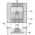
- FIG. 3A is a top view and a side view of the charge shield 107 provided in the three-dimensional additive manufacturing apparatus according to the present embodiment.
- the side surface shape of the charge shield 107 is a flat plate shape and has a thickness of 0.5 mm or less, but it may be thinner or thicker. In order to suppress the inflow of heat from the modeling surface, the thickness is reduced to suppress the inflow of heat from the modeling surface.
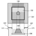
- FIG. 3B is a top view and a side view of another example of the charge shield 107 provided in the three-dimensional additive manufacturing apparatus according to the present embodiment.
- a contact 171 is attached to the lower surface of the charge shield 107 shown in FIG.
- the charge shield 107 has a shape that linearly contacts the presintered region with the contact 171 and contacts the presintered region with the contact 171, so that the contact area between the charge shield 107 and the presintered region is becomes smaller. Since the contact area between the charge shield 107 and the modeling surface (temporary sintering region) becomes small, the inflow of heat from the modeling surface can be suppressed.
- FIG. 3C is a top view and a side view of still another example of the charge shield 107 provided in the three-dimensional additive manufacturing apparatus according to the present embodiment.
- FIG. 3C shows the contact of the flat-shaped charge shield 107 shown in FIG. 3A by attaching a plurality of thin needle-like contacts on the lower side of the flat plate or by using a brush-like (comb-like) contact. The area is further reduced. Thus, the inflow of heat can be suppressed by reducing the contact area between the charge shield 107 and the modeling surface.
- the modeling plate 106 (modeling surface) is represented by a rectangular shape, but the same applies to a circular shape or a polygonal shape.
- FIG. 6 is a flowchart for explaining the processing procedure of the three-dimensional additive manufacturing apparatus according to this embodiment.
- the three-dimensional additive manufacturing apparatus 100 acquires modeling data of the three-dimensional additive manufacturing object 130.
- the three-dimensional additive manufacturing apparatus 100 spreads and spreads metal powder on the modeling surface.
- the three-dimensional additive manufacturing apparatus 100 lowers the charge shield 107 to contact the modeling surface.
- the three-dimensional additive manufacturing apparatus 100 performs pre-sintering by irradiating an electron beam.
- step S609 based on the acquired modeling data, an electron beam is irradiated and main melting of the metal powder for one layer is implemented.
- step S ⁇ b> 611 the three-dimensional additive manufacturing apparatus 100 raises the charge shield 107 and spreads and spreads metal powder on the modeling surface while moving the linear funnel 105.
- step S613 the three-dimensional additive manufacturing apparatus 100 performs temporary sintering and main melting of the spread metal powder to melt and solidify one layer of metal powder.
- step S615 the three-dimensional additive manufacturing apparatus 100 determines whether or not the three-dimensional additive object 130 has been formed. When it is determined that the process has been completed (YES in step S615), the three-dimensional additive manufacturing apparatus 100 ends the process. When it is determined that the process has not been completed (NO in step S615), the three-dimensional additive manufacturing apparatus 100 repeats the processes in and after step S611.
- the unsintered powder between the modeling plate and the modeling frame base is masked by the charge shield that is a conductive material. Charge up of the sintered powder 152 can be suppressed, and smoke can be prevented.
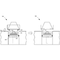
- FIG. 7 is a partially enlarged view for explaining the configuration of the three-dimensional additive manufacturing apparatus 700 according to this embodiment.
- the charge shield 107 is moved up and down, but in this embodiment, as shown in FIG. 7, a charge shield (shield plate) 707 having fulcrums (rotating shafts) on four sides. However, it is attached so that it may hang down with respect to a modeling surface. In a state where the charge shield 707 is in contact with the modeling surface, the four corners overlap, and the unsintered region cannot be seen from above.
- the rotation axis of the rotary shaft is controlled by a vacuum-compatible motor, a non-vacuum motor, or the like. Rotate and move upward.
- the device configuration can be simplified. Further, when the modeling surface is irradiated with an electron beam, the unsintered powder between the modeling plate and the modeling frame is masked with a charge shield that is a conductive material. Charge up can be suppressed and smoke can be prevented.
- FIG. 8 is a partially enlarged view for explaining the configuration of the three-dimensional additive manufacturing apparatus 800 according to this embodiment.
- the three-dimensional additive manufacturing apparatus 800 includes a linear funnel 805 and a charge shield 807. Further, the linear funnel 805 is provided with a linear motion cam (original node) 853, and the charge shield 807 is provided with a linear motion cam (follower node) 873.
- the charge shield 807 moves upward in accordance with the movement of the linear funnel 805. In this case, the unsintered region is always covered with the charge shield 807.
- the linear cam 853 provided on the linear funnel 805 pushes up the linear cam 873 provided on the charge shield 807 side. That is, the charge shield 807 moves up and down according to the movement of the linear funnel 805 provided with the linear motion cam 853.
- a roller may be provided on either one or both.
- the charge shield 807 covers the unsintered region except when the metal powder is spread.
- the electron beam control and the charge shield 807 control may be linked so that the electron beam can be irradiated only when the charge shield 807 covers the modeling surface. Detection of whether or not the charge shield 807 has reached the modeling surface may be mechanically detected by, for example, a limit switch.
- the charge shield lifting mechanism is not required, and a simple device configuration can be achieved.
- the movement can be easily synchronized.
- the unsintered powder between the modeling plate and the modeling frame is masked with a charge shield, which is a conductive material, so that the unsintered region is charged with the unsintered powder. Up can be suppressed and smoke can be prevented.
- the present invention may be applied to a system composed of a plurality of devices, or may be applied to a single device. Furthermore, the present invention can also be applied to a case where an information processing program that implements the functions of the embodiments is supplied directly or remotely to a system or apparatus. Therefore, in order to realize the functions of the present invention on a computer, a program installed on the computer, a medium storing the program, and a WWW (World Wide Web) server that downloads the program are also included in the scope of the present invention. . In particular, at least a non-transitory computer readable medium storing a program for causing a computer to execute the processing steps included in the above-described embodiments is included in the scope of the present invention.
Landscapes
- Engineering & Computer Science (AREA)
- Chemical & Material Sciences (AREA)
- Manufacturing & Machinery (AREA)
- Materials Engineering (AREA)
- Mechanical Engineering (AREA)
- Physics & Mathematics (AREA)
- Plasma & Fusion (AREA)
- Powder Metallurgy (AREA)
Abstract
未焼結領域がチャージアップされることを効果的に防止する。3次元積層造形装置であって、3次元積層造形物が造形される造形面上に、前記3次元積層造形物の材料を散布する線状漏斗を備える。また、3次元積層造形装置は、電子ビームを発生させる電子銃を備える。さらに、3次元積層造形装置は、前記電子ビームを前記材料に照射する際に、前記造形面上に散布された前記材料をシールドするチャージシールドを備える。さらにまた、チャージシールドを昇降させる昇降機構を備える。
Description
本発明は、3次元積層造形装置、3次元積層造形装置の制御方法および3次元積層造形装置の制御プログラムに関する。
上記技術分野において、特許文献1には、真空室内に補助ガスとして不活性ガスを導入する技術が開示されている。
しかしながら、上記文献に記載の技術では、未焼結領域がチャージアップされることを効果的にを防止することができなかった。
本発明の目的は、上述の課題を解決する技術を提供することにある。
上記目的を達成するため、本発明に係る3次元積層造形装置は、
3次元積層造形物が造形される造形面上に、前記3次元積層造形物の材料を散布する材料散布手段と、
電子ビームを発生させる電子銃と、
前記電子ビームを前記材料に照射する際に、前記造形面上に散布された前記材料をシールドするシールド手段と、
を備える。
3次元積層造形物が造形される造形面上に、前記3次元積層造形物の材料を散布する材料散布手段と、
電子ビームを発生させる電子銃と、
前記電子ビームを前記材料に照射する際に、前記造形面上に散布された前記材料をシールドするシールド手段と、
を備える。
上記目的を達成するため、本発明に係る3次元積層造形装置の制御方法は、
3次元積層造形物が造形される造形面上に、前記3次元積層造形物の材料を材料散布手段により散布する材料散布ステップと、
電子銃により電子ビームを発生させる発生ステップと、
前記電子ビームを前記材料に照射する際に、前記造形面上に散布された前記材料をシールド手段によりシールドするシールドステップと、
を含む。
3次元積層造形物が造形される造形面上に、前記3次元積層造形物の材料を材料散布手段により散布する材料散布ステップと、
電子銃により電子ビームを発生させる発生ステップと、
前記電子ビームを前記材料に照射する際に、前記造形面上に散布された前記材料をシールド手段によりシールドするシールドステップと、
を含む。
上記目的を達成するため、本発明に係る3次元積層造形装置の制御プログラムは、
3次元積層造形物が造形される造形面上に、前記3次元積層造形物の材料を材料散布手段により散布させる材料散布ステップと、
電子銃により電子ビームを発生させる発生ステップと、
前記電子ビームを前記材料に照射する際に、前記造形面上に散布された前記材料をシールド手段によりシールドさせるシールドステップと、
をコンピュータに実行させる。
3次元積層造形物が造形される造形面上に、前記3次元積層造形物の材料を材料散布手段により散布させる材料散布ステップと、
電子銃により電子ビームを発生させる発生ステップと、
前記電子ビームを前記材料に照射する際に、前記造形面上に散布された前記材料をシールド手段によりシールドさせるシールドステップと、
をコンピュータに実行させる。
本発明によれば、未焼結領域がチャージアップされることを効果的に防止できる。
以下に、本発明を実施するための形態について、図面を参照して、例示的に詳しく説明記載する。ただし、以下の実施の形態に記載されている、構成、数値、処理の流れ、機能要素などは一例に過ぎず、その変形や変更は自由であって、本発明の技術範囲を以下の記載に限定する趣旨のものではない。
[第1実施形態]
本発明の第1実施形態としての3次元積層造形装置100について、図1を用いて説明する。3次元積層造形装置100は、パウダーベッド方式の装置である。3次元積層造形装置100は、リコータなどにより造形面上に敷き詰めた材料に電子ビームを照射して、材料を溶融し、凝固させ、1層分の材料の積層を完成させる。そして、1層分の積層が完了したら、3次元積層造形装置100は、1層分の高さに相当する高さだけ造形台を下げて、次の層の材料をリコータなどにより敷き詰める(散布する)。材料を敷き詰めたら、電子ビームを照射して、材料を溶融し、凝固させ、次の1層分の材料の積層を完成させる。3次元積層造形装置100は、この動作を繰り返して、所望の3次元積層造形物を造形する。
本発明の第1実施形態としての3次元積層造形装置100について、図1を用いて説明する。3次元積層造形装置100は、パウダーベッド方式の装置である。3次元積層造形装置100は、リコータなどにより造形面上に敷き詰めた材料に電子ビームを照射して、材料を溶融し、凝固させ、1層分の材料の積層を完成させる。そして、1層分の積層が完了したら、3次元積層造形装置100は、1層分の高さに相当する高さだけ造形台を下げて、次の層の材料をリコータなどにより敷き詰める(散布する)。材料を敷き詰めたら、電子ビームを照射して、材料を溶融し、凝固させ、次の1層分の材料の積層を完成させる。3次元積層造形装置100は、この動作を繰り返して、所望の3次元積層造形物を造形する。
<前提技術>
図4は、本実施形態に係る3次元積層造形装置の前提技術に係る3次元積層造形装置の構成の一例を示す図である。
図4は、本実施形態に係る3次元積層造形装置の前提技術に係る3次元積層造形装置の構成の一例を示す図である。
≪構成≫
真空容器401に電子銃402が装着されており、真空容器401内には断面が円状または角状の造形枠台(造形ボックス)403が設けられている。造形枠台403の内側下方にはZ軸駆動機構404があり、粉末台440をラックアンドピニオンやボールねじなどによりZ方向に駆動することができる。
真空容器401に電子銃402が装着されており、真空容器401内には断面が円状または角状の造形枠台(造形ボックス)403が設けられている。造形枠台403の内側下方にはZ軸駆動機構404があり、粉末台440をラックアンドピニオンやボールねじなどによりZ方向に駆動することができる。
造形枠台403と粉末台440との隙間には、耐熱性のあるフレキシブルシール460があり、フレキシブルシール460と造形枠台403の内面のすべり面で摺動性と密閉性とを持たせている。真空容器401は、図示しない真空ポンプにより排気され、真空容器401内は真空に維持されている。
粉末台440には、金属粉末で浮かせた状態で、3次元積層造形物430が造形される造形プレート(ベースプレート)406が配置されている。造形プレート406は、電気的に浮かないようにGND線450でGND電位である粉末台440に接地されている。造形プレート406上には3次元積層造形物430が造形され、各層の造形時には、金属粉末を充填した線状漏斗(リコータ)405により、造形枠台403上面とほぼ同じ高さまで、金属粉末が敷き詰められている(敷き詰められた粉末452)。
線状漏斗405には、図示しない金属粉末用ホッパから適宜金属粉末が補充されている。3次元積層造形物430は、一層分、敷き詰められた粉末(未焼結)452を電子銃402からの電子ビームにより、3次元積層造形物430となる領域を2次元的に溶融し、その重ね合わせによって構築される。造形プレート406上に敷き詰められた粉末452の3次元積層造形物430以外の領域は、電子銃402からの電子ビームにより、仮焼結された粉末(敷き詰められた粉末(仮焼結))451であり、導電性を有している。
造形面と電子銃402との間には、防着カバー420が取り付けられており、造形時に発生する金属蒸気やファイヤーワークスによる金属スパッタの真空容器401の内壁への蒸着を防いでいる。
≪動作≫
3方向を金属粉末で覆われた造形プレート406上面を造形枠台403上面とほぼ同じ高さに配置し、電子銃402からの電子ビームを造形プレート406上面全域より少し狭い領域に照射し、金属粉末が仮焼結する程度の温度まであらかじめ昇温しておく。
3方向を金属粉末で覆われた造形プレート406上面を造形枠台403上面とほぼ同じ高さに配置し、電子銃402からの電子ビームを造形プレート406上面全域より少し狭い領域に照射し、金属粉末が仮焼結する程度の温度まであらかじめ昇温しておく。
造形の開始時は、造形プレート406上面が造形枠台403上面より僅かに下がった位置に配置するように粉末台440をZ軸駆動機構404により下げる。この僅かに下がったΔZが、その後のZ方向の層厚に相当する。金属粉末を充填した線状漏斗405を造形プレート406の上面に沿って反対側に移動させ、ΔZ分の金属粉末が敷き詰められた造形プレート406より少し狭い領域に電子銃402からの電子ビームを照射し、昇温させて、照射領域の金属粉末を確実に仮焼結させる。
あらかじめ準備された設計上の3次元積層造形物(造形モデル)をΔZ間隔でスライスした2次元形状に従い、電子銃402からの電子ビームにより、その2次元領域を溶融する。1層分の溶融および凝固後、再び、造形プレート406より少し狭い領域に電子銃402からの電子ビームを照射し、昇温させて、金属粉末の敷き詰めの準備をする。
所定の温度に昇温後、電子ビームをOFFにして、Z軸駆動機構404により粉末台440をΔZ分下げ、線状漏斗405を再び造形枠台403の上面に沿って反対に移動させ、ΔZ分の金属粉末を前層の上に敷き詰める。そして、電子銃402からの電子ビームにより確実に仮焼結後、その層に相当する2次元形状の領域を溶融する。これを繰り返して、3次元積層造形物430を造形する。
図5は、本実施形態に係る3次元積層造形装置の前提技術に係る3次元積層造形装置によるスモーク現象発生のメカニズムを説明する図である。図5は、図4の電子銃402の下部の拡大図である。図示したように、仮焼結や溶融時に電子ビームを照射した際に、照射位置から反射電子や2次電子が大量に発生する。反射電子は、上部の防着カバー420内壁に当たり、更なる反射電子、2次電子が放出される。
このように、防着カバー420で覆われた造形面上方には大量の電子が存在しており、仮焼結されていない金属粉末は表面の酸化膜により個々の粉末間は電気的に絶縁状態となるため、容易にマイナスにチャージする。そのため、電子ビームを照射する領域に仮焼結不十分によるチャージした金属粉末ができると、そのチャージした金属粉末は、外側の未焼結領域に吹き飛ばされ、その領域でのチャージのバランスが崩れる。そして、チャージのバランスが崩れると、静電気力による斥力バランスも崩れ、金属粉末同士の反発でそれらが飛び散るスモークという現象が発生する。これを抑制するため、Heガスなどのガスを導入してガスイオンを生成し中和作用に期待した手法が用いられているが、仮焼結不十分の場合には、依然としてスモーク現象が発生する。
<本実施形態に係る技術>
≪構成≫
図1は、本実施形態に係る3次元積層造形装置の構成を示す図である。図2は、本実施形態に係る3次元積層造形装置の構成を示す部分拡大図である。3次元積層造形装置100は、真空容器101と、電子銃102と、造形枠台103と、Z軸駆動機構104と、線状漏斗105と、造形プレート106と、チャージシールド107とを備える。なお、以下の説明においては、3次元積層造形装置100として、パウダーベッド方式の造形装置を例に説明をする。
≪構成≫
図1は、本実施形態に係る3次元積層造形装置の構成を示す図である。図2は、本実施形態に係る3次元積層造形装置の構成を示す部分拡大図である。3次元積層造形装置100は、真空容器101と、電子銃102と、造形枠台103と、Z軸駆動機構104と、線状漏斗105と、造形プレート106と、チャージシールド107とを備える。なお、以下の説明においては、3次元積層造形装置100として、パウダーベッド方式の造形装置を例に説明をする。
チャージシールド107は、上面から見ると略矩形形状をしており、造形プレート106上に電子ビームが到達するように、造形プレート106の形状に合わせて内側開口部がある。チャージシールド107の内側開口部は、チャージシールド107の中央近傍に位置しており、例えば、造形プレート106が円形であれば円形の開口部となり、矩形であれば矩形の開口部となる。また、チャージシールド107は、側面から見ると平板状の形状をしている。
そして、チャージシールド107は、造形枠台103と造形プレート106との間の領域にできる未焼結粉末152で構成される未焼結領域を覆う、すなわち、シールドマスクである。また、チャージシールド107には開口部が設けられているので、造形枠台103と造形プレート106との間の領域にできる仮焼結粉末151で構成される仮焼結領域は覆われない。チャージシールド107の材質は、例えば、金属などの導電性材料やステンレスなどの合金などが代表的であり、好ましくは、3次元積層造形物130の材料である金属粉末と同種の材料がよいが、シールドとしての役割を果たす材料であればこれらには限定されない。
チャージシールド107には、不図示の上下駆動機構(昇降機構)が取り付けられており、チャージシールド107は、造形プレート106上に電子ビームを照射する場合に、下降してきて、造形面上に移動する。また、図示していないが、チャージシールド107は、電気的にGNDに接地されている。
≪動作≫
3方向を金属粉末で覆われた造形プレート106上面を造形枠台103上面とほぼ同じ高さに配置し、チャージシールド107を造形プレート106上面まで降ろし、造形プレート106と造形枠台103との間にある金属粉末を覆う。このとき、チャージシールド107は、金属粉末に接触させておく。電子銃102からの電子ビームを造形プレート106上面全域より少し狭い領域(チャージシールド107内側開口部には電子ビームを当てない領域)に照射し、金属粉末が完全に仮焼結する程度の温度まで造形プレート106をあらかじめ昇温させておく。
3方向を金属粉末で覆われた造形プレート106上面を造形枠台103上面とほぼ同じ高さに配置し、チャージシールド107を造形プレート106上面まで降ろし、造形プレート106と造形枠台103との間にある金属粉末を覆う。このとき、チャージシールド107は、金属粉末に接触させておく。電子銃102からの電子ビームを造形プレート106上面全域より少し狭い領域(チャージシールド107内側開口部には電子ビームを当てない領域)に照射し、金属粉末が完全に仮焼結する程度の温度まで造形プレート106をあらかじめ昇温させておく。
造形開始時には、造形プレート106上面が造形枠台103上面より僅かに下がった位置に配置されるように、粉末台140をZ軸駆動機構104により下げる。この僅かに下がったΔZが、その後のZ方向の層厚に相当する。
チャージシールド107を上方に移動し、金属粉末を充填した線状漏斗(リコータ)105を造形プレート106の上面に沿って反対側に移動させ、ΔZ分の金属粉末を造形プレート106上とその周りに散布して、敷き詰める。線状漏斗105が、チャージシールド107の外側に抜けた後、チャージシールド107を再び造形面まで下げ、造形プレート106と造形枠台103との間の金属粉末を覆う。
造形プレート106上に敷き詰めた金属粉末に対して、チャージシールド107の内側開口部に電子ビームが当たらない程度の領域に電子銃102からの電子ビームを照射して、昇温させ、照射領域の金属粉末を確実に仮焼結させる。
あらかじめ準備された設計上の3次元積層造形物(造形モデル)をΔZ間隔でスライスした2次元形状に従い、電子銃102からの電子ビームにより、その2次元形状領域を溶融する。1層分、溶融および凝固後、再び造形プレート106より少し狭い領域に電子銃102からの電子ビームを照射し、昇温して、金属粉末敷き詰めの準備をする。所定の温度に昇温後、電子ビームをOFFにして、チャージシールド107を上方に移動する。
Z軸駆動機構104により粉末台140をΔZ分下げて、線状漏斗105を再び造形枠台103の上面に沿って反対側に移動させ、ΔZ分の金属粉末を前層の上に敷き詰め、チャージシールド107を再び造形面まで下げる。チャージシールド107の内側開口部に電子ビームが当たらない程度の領域に電子銃102からの電子ビームを照射し、新たに敷かれた金属粉末を確実に仮焼結した後、その層に相当する2次元形状の領域を溶融する。3次元積層造形装置100は、これを繰り返して、3次元積層造形物130を造形する。また、チャージシールド107の開口部の外側のマスク部にヒータを設けたり、埋め込んだりして、マスク部の下部(マスク部内側)の金属粉末の温度を造形面と同等の温度に昇温してもよい。これにより、チャージシールド107で造形プレート106と造形枠台103との間の金属粉末を覆った際の、造形面(金属粉末)の温度の低下(大きな変化)を抑制する。
チャージシールド107の材質としては、熱伝導率が小さく、熱耐性に優れた導電性材料が望ましく、例えば、チタンや64Tiなどのチタン合金などや、ステンレス鋼などである。なお、ここではチャージシールド107を上下方向に移動させる例で説明をしたが、チャージシールド107の移動方向はこれには限定されず、例えば、左右方向や、奥行き方向などへ移動させてもよい。
図3Aは、本実施形態に係る3次元積層造形装置の備えるチャージシールド107の上面図および側面図である。チャージシールド107の側面形状は平板状の形状であり、厚みは0.5mm以下となっているが、これより薄くても、厚くてもよい。なお、造形面からの熱の流入を抑えるため、厚みを薄くして造形面からの熱の流入を抑えている。
図3Bは、本実施形態に係る3次元積層造形装置の備えるチャージシールド107の他の例の上面図および側面図である。同図に示したチャージシールド107の下面(造形面に近い側の面)に接触子171が取り付けられている。そして、チャージシールド107は、接触子171で仮焼結領域に線状に接触する形状であり、接触子171で仮焼結領域に接触するので、チャージシールド107と仮焼結領域との接触面積が小さくなる。チャージシールド107と造形面(仮焼結領域)との接触面積が小さくなるので、造形面からの熱の流入を抑えられる。
図3Cは、本実施形態に係る3次元積層造形装置の備えるチャージシールド107のさらに他の例の上面図および側面図である。図3Cは、図3Aに示した平板形状のチャージシールド107において、平板の下側に細いニードル状の接触子を複数本付けたり、ブラシ状(櫛状)の接触子としたりすることにより、接触面積をさらに小さくしている。このように、チャージシールド107と造形面との接触面積を小さくすることにより、熱の流入を抑制できる。
なお、図3A乃至図3Cでは造形プレート106(造形面)を矩形状で表したが、円形状や多角形状などであっても同様である。
図6は、本実施形態に係る3次元積層造形装置の処理手順を説明するフローチャートである。ステップS601において、3次元積層造形装置100は、3次元積層造形物130の造形データを取得する。ステップS603において、3次元積層造形装置100は、金属粉末を造形面に散布して、敷き詰める。ステップS605において、3次元積層造形装置100は、チャージシールド107を降下させて、造形面に接触させる。ステップS607において、3次元積層造形装置100は、電子ビームを照射して、仮焼結を実施する。ステップS609において、取得した造形データに基づいて、電子ビームを照射して、1層分の金属粉末の本溶融を実施する。ステップS611において、3次元積層造形装置100は、チャージシールド107を上昇させ、線状漏斗105を移動させながら造形面上に金属粉末を散布して、敷き詰める。ステップS613において、3次元積層造形装置100は、敷き詰めた金属粉末の仮焼結・本溶融を実施し、1層分の金属粉末を溶融し、凝固させる。ステップS615において、3次元積層造形装置100は、3次元積層造形物130の造形が終了したか否かを判断する。終了したと判断した場合(ステップS615のYES)、3次元積層造形装置100は、処理を終了する。終了していないと判断した場合(ステップS615のNO)、3次元積層造形装置100は、ステップS611以下の処理を繰り返す。
本実施形態によれば、造形面に電子ビームを照射する場合、造形プレートと造形枠台との間の未焼結粉末を導電性材料であるチャージシールドでマスクするので、未焼結領域の未焼結粉末152のチャージアップを抑制でき、スモークを防止できる。
[第2実施形態]
次に本発明の第2実施形態に係る3次元積層造形装置について、図7を用いて説明する。図7は、本実施形態に係る3次元積層造形装置700の構成を説明するための部分拡大図である。第1実施形態では、チャージシールド107を上下に移動させていたが、本実施形態においては、図7に示したように、4辺に支点(回転軸)を持ったチャージシールド(シールド板)707が、造形面に対して垂れ下がるように取り付けられている。チャージシールド707が造形面に接している状態で4隅が重なり合い、上方から未焼結領域が見えない状態となる。回転軸は、真空対応モータや真空外モータなどから回転角が制御され、材料散布部である線状漏斗105が造形面に金属粉末を敷く際には、チャージシールド707は回転軸を中心にして回動し、上方に移動する。
次に本発明の第2実施形態に係る3次元積層造形装置について、図7を用いて説明する。図7は、本実施形態に係る3次元積層造形装置700の構成を説明するための部分拡大図である。第1実施形態では、チャージシールド107を上下に移動させていたが、本実施形態においては、図7に示したように、4辺に支点(回転軸)を持ったチャージシールド(シールド板)707が、造形面に対して垂れ下がるように取り付けられている。チャージシールド707が造形面に接している状態で4隅が重なり合い、上方から未焼結領域が見えない状態となる。回転軸は、真空対応モータや真空外モータなどから回転角が制御され、材料散布部である線状漏斗105が造形面に金属粉末を敷く際には、チャージシールド707は回転軸を中心にして回動し、上方に移動する。
本実施形態によれば、回転軸によりチャージシールドを移動させるので、装置構成をシンプルにすることができる。また、造形面に電子ビームを照射する場合、造形プレートと造形枠台との間の未焼結粉末を導電性材料であるチャージシールドでマスクするので、未焼結領域の未焼結粉末152のチャージアップを抑制でき、スモークを防止できる。
[第3実施形態]
次に本発明の第3実施形態に係る3次元積層造形装置について、図8を用いて説明する。図8は、本実施形態に係る3次元積層造形装置800の構成を説明するための部分拡大図である。3次元積層造形装置800は、線状漏斗805と、チャージシールド807とを備える。また、線状漏斗805には直動カム(原節)853が設けられ、チャージシールド807には直動カム(従節)873が設けられている。
次に本発明の第3実施形態に係る3次元積層造形装置について、図8を用いて説明する。図8は、本実施形態に係る3次元積層造形装置800の構成を説明するための部分拡大図である。3次元積層造形装置800は、線状漏斗805と、チャージシールド807とを備える。また、線状漏斗805には直動カム(原節)853が設けられ、チャージシールド807には直動カム(従節)873が設けられている。
本実施形態においては、線状漏斗805により金属粉末を敷き詰める際に、線状漏斗805の動きに合わせてチャージシールド807が上方に移動する。この場合、未焼結領域が、チャージシールド807により常時覆われている。そして、造形面上に線状漏斗805で金属粉末を敷き詰める場合、線状漏斗805に設けられた直動カム853が、チャージシールド807側に設けられた直動カム873を押し上げる。つまり、直動カム853が設けられた線状漏斗805の動きに応じて、チャージシールド807が上下動する。
したがって、線状漏斗805が造形面上を通過する場合のみチャージシールド807が造形面から離れる。なお、直動カム853と直動カム873との摩擦を小さくするため、どちらか一方または双方にローラを設けてもよい。
このような構成とすることにより、金属粉末を敷き詰める場合以外は、チャージシールド807が未焼結領域を覆うことになる。しかしながら、フェイルセーフを実現するため、電子ビームの制御とチャージシールド807の制御とをリンクさせ、チャージシールド807が造形面を覆っているときのみ、電子ビームの照射を可能としてもよい。チャージシールド807が造形面に達しているか否かの検出は、例えば、リミットスイッチなどで機械的に検出してもよい。
本実施形態によれば、線状漏斗およびチャージシールドに直動カムを設けたので、チャージシールドの昇降機構が不要となり、シンプルな装置構成とすることができ、線状漏斗の動きとチャージシールドの動きとを容易に同期させることができる。また、造形面に電子ビームを照射する場合、造形プレートと造形枠台との間の未焼結粉末を導電性材料であるチャージシールドでマスクするので、未焼結領域の未焼結粉末のチャージアップを抑制でき、スモークを防止できる。
[他の実施形態]
以上、実施形態を参照して本願発明を説明したが、本願発明は上記実施形態に限定されるものではない。本願発明の構成や詳細には、本願発明のスコープ内で当業者が理解し得る様々な変更をすることができる。また、それぞれの実施形態に含まれる別々の特徴を如何様に組み合わせたシステムまたは装置も、本発明の範疇に含まれる。
以上、実施形態を参照して本願発明を説明したが、本願発明は上記実施形態に限定されるものではない。本願発明の構成や詳細には、本願発明のスコープ内で当業者が理解し得る様々な変更をすることができる。また、それぞれの実施形態に含まれる別々の特徴を如何様に組み合わせたシステムまたは装置も、本発明の範疇に含まれる。
また、本発明は、複数の機器から構成されるシステムに適用されてもよいし、単体の装置に適用されてもよい。さらに、本発明は、実施形態の機能を実現する情報処理プログラムが、システムあるいは装置に直接あるいは遠隔から供給される場合にも適用可能である。したがって、本発明の機能をコンピュータで実現するために、コンピュータにインストールされるプログラム、あるいはそのプログラムを格納した媒体、そのプログラムをダウンロードさせるWWW(World Wide Web)サーバも、本発明の範疇に含まれる。特に、少なくとも、上述した実施形態に含まれる処理ステップをコンピュータに実行させるプログラムを格納した非一時的コンピュータ可読媒体(non-transitory computer readable medium)は本発明の範疇に含まれる。
Claims (9)
- 3次元積層造形物が造形される造形面上に、前記3次元積層造形物の材料を散布する材料散布手段と、
電子ビームを発生させる電子銃と、
前記電子ビームを前記材料に照射する際に、前記造形面上に散布された前記材料をシールドするシールド手段と、
を備える3次元積層造形装置。 - 前記シールド手段を昇降させる昇降手段をさらに備える請求項1に記載の3次元積層造形装置。
- 前記シールド手段は、支点を中心にして回動する平板である請求項1に記載の3次元積層造形装置。
- 前記材料散布手段に直動カムが設けられ、
前記シールド手段は、前記材料散布手段の動きに応じて、上下動する請求項1に記載の3次元積層造形装置。 - 前記シールド手段は、前記造形面上に散布された前記材料のうち、前記電子ビームにより焼結しない未焼結領域をシールドする請求項1乃至4のいずれか1項に記載の3次元積層造形装置。
- 前記シールド手段は、ヒータを有する請求項1乃至5のいずれか1項に記載の3次元積層造形装置。
- 前記シールド手段は、矩形または円形の平板であり、中央近傍に開口部を有する請求項1乃至6のいずれか1項に記載の3次元積層造形装置。
- 3次元積層造形物が造形される造形面上に、前記3次元積層造形物の材料を材料散布手段により散布する材料散布ステップと、
電子銃により電子ビームを発生させる発生ステップと、
前記電子ビームを前記材料に照射する際に、前記造形面上に散布された前記材料をシールド手段によりシールドするシールドステップと、
を含む3次元積層造形装置の制御方法。 - 3次元積層造形物が造形される造形面上に、前記3次元積層造形物の材料を材料散布手段により散布させる材料散布ステップと、
電子銃により電子ビームを発生させる発生ステップと、
前記電子ビームを前記材料に照射する際に、前記造形面上に散布された前記材料をシールド手段によりシールドさせるシールドステップと、
をコンピュータに実行させる3次元積層造形装置の制御プログラム。
Priority Applications (4)
| Application Number | Priority Date | Filing Date | Title |
|---|---|---|---|
| US15/122,661 US10610957B2 (en) | 2016-03-25 | 2016-03-25 | Three-dimensional laminating and shaping apparatus, three-dimensional laminating and shaping apparatus control method, and three-dimensional laminating and shaping apparatus control program |
| EP16825687.3A EP3248716B1 (en) | 2016-03-25 | 2016-03-25 | Three-dimensional additive manufacturing device, control method for three-dimensional additive manufacturing device, and control program for three-dimensional additive manufacturing device |
| JP2016547110A JP6216464B1 (ja) | 2016-03-25 | 2016-03-25 | 3次元積層造形装置、3次元積層造形装置の制御方法および3次元積層造形装置の制御プログラム |
| PCT/JP2016/059642 WO2017163402A1 (ja) | 2016-03-25 | 2016-03-25 | 3次元積層造形装置、3次元積層造形装置の制御方法および3次元積層造形装置の制御プログラム |
Applications Claiming Priority (1)
| Application Number | Priority Date | Filing Date | Title |
|---|---|---|---|
| PCT/JP2016/059642 WO2017163402A1 (ja) | 2016-03-25 | 2016-03-25 | 3次元積層造形装置、3次元積層造形装置の制御方法および3次元積層造形装置の制御プログラム |
Publications (1)
| Publication Number | Publication Date |
|---|---|
| WO2017163402A1 true WO2017163402A1 (ja) | 2017-09-28 |
Family
ID=59901224
Family Applications (1)
| Application Number | Title | Priority Date | Filing Date |
|---|---|---|---|
| PCT/JP2016/059642 Ceased WO2017163402A1 (ja) | 2016-03-25 | 2016-03-25 | 3次元積層造形装置、3次元積層造形装置の制御方法および3次元積層造形装置の制御プログラム |
Country Status (4)
| Country | Link |
|---|---|
| US (1) | US10610957B2 (ja) |
| EP (1) | EP3248716B1 (ja) |
| JP (1) | JP6216464B1 (ja) |
| WO (1) | WO2017163402A1 (ja) |
Cited By (2)
| Publication number | Priority date | Publication date | Assignee | Title |
|---|---|---|---|---|
| WO2020059060A1 (ja) * | 2018-09-19 | 2020-03-26 | 技術研究組合次世代3D積層造形技術総合開発機構 | 金属積層造形用粉末の評価方法、評価プログラムおよび製造方法、情報処理装置および金属積層造形装置 |
| JP2022047820A (ja) * | 2020-09-14 | 2022-03-25 | 日本電子株式会社 | 三次元積層造形装置および三次元積層造形方法 |
Families Citing this family (6)
| Publication number | Priority date | Publication date | Assignee | Title |
|---|---|---|---|---|
| US11059123B2 (en) * | 2017-04-28 | 2021-07-13 | Arcam Ab | Additive manufacturing of three-dimensional articles |
| US11426818B2 (en) | 2018-08-10 | 2022-08-30 | The Research Foundation for the State University | Additive manufacturing processes and additively manufactured products |
| JP7008669B2 (ja) * | 2019-09-09 | 2022-01-25 | 日本電子株式会社 | 3次元積層造形装置及び3次元積層造形方法 |
| WO2021113151A2 (en) * | 2019-12-03 | 2021-06-10 | Nikon Corporation | Additive manufacturing system with thermal control of material |
| US11925981B2 (en) | 2020-06-29 | 2024-03-12 | Arcam Ab | Method, apparatus and control unit for selectively sintering a powder layer in additive manufacturing processes to achieve a future, desired heat conductivity |
| JP2026014792A (ja) * | 2024-07-19 | 2026-01-29 | 日本電子株式会社 | 3次元積層造形装置 |
Citations (4)
| Publication number | Priority date | Publication date | Assignee | Title |
|---|---|---|---|---|
| JPH06136520A (ja) * | 1992-10-23 | 1994-05-17 | Matsushita Electric Ind Co Ltd | 薄膜の製造方法及び製造装置 |
| JP2008107208A (ja) * | 2006-10-25 | 2008-05-08 | Shimadzu Corp | 電子ビーム走査方法、電子ビーム走査装置、およびtftアレイ検査装置 |
| JP2010526694A (ja) | 2007-05-15 | 2010-08-05 | アルカム アーベー | 3次元物体を作るための方法及び装置 |
| JP2015175012A (ja) * | 2014-03-13 | 2015-10-05 | 日本電子株式会社 | 3次元積層造形装置及び3次元積層造形方法 |
Family Cites Families (7)
| Publication number | Priority date | Publication date | Assignee | Title |
|---|---|---|---|---|
| DE2211597C3 (de) | 1972-03-10 | 1975-07-10 | Steigerwald Strahltechnik Gmbh, 8000 Muenchen | Einrichtung zum Freihalten des Strahlwegs und der unmittelbaren Umgebung des Strahlwegs eines Strahls einer Energiestrahl-Materialbearbeitungsmaschine von störender Materie |
| US4976843A (en) * | 1990-02-02 | 1990-12-11 | Micrion Corporation | Particle beam shielding |
| US6326635B1 (en) * | 1999-07-30 | 2001-12-04 | Etec Systems, Inc. | Minimization of electron fogging in electron beam lithography |
| US20040262261A1 (en) * | 2003-06-27 | 2004-12-30 | Fink Jeffrey E. | Methods and systems for creating layer-formed plastic elements with improved properties |
| DE102006055054A1 (de) * | 2006-11-22 | 2008-05-29 | Eos Gmbh Electro Optical Systems | Vorrichtung zum schichtweisen Herstellen eines dreidimensionalen Objekts |
| DE102012012363A1 (de) * | 2012-06-22 | 2013-12-24 | Voxeljet Technology Gmbh | Vorrichtung zum Aufbauen eines Schichtenkörpers mit entlang des Austragbehälters bewegbarem Vorrats- oder Befüllbehälter |
| WO2017081812A1 (ja) | 2015-11-13 | 2017-05-18 | 技術研究組合次世代3D積層造形技術総合開発機構 | 3次元積層造形装置、3次元積層造形装置の製造方法および3次元積層造形装置の製造プログラム |
-
2016
- 2016-03-25 WO PCT/JP2016/059642 patent/WO2017163402A1/ja not_active Ceased
- 2016-03-25 US US15/122,661 patent/US10610957B2/en active Active
- 2016-03-25 EP EP16825687.3A patent/EP3248716B1/en active Active
- 2016-03-25 JP JP2016547110A patent/JP6216464B1/ja active Active
Patent Citations (4)
| Publication number | Priority date | Publication date | Assignee | Title |
|---|---|---|---|---|
| JPH06136520A (ja) * | 1992-10-23 | 1994-05-17 | Matsushita Electric Ind Co Ltd | 薄膜の製造方法及び製造装置 |
| JP2008107208A (ja) * | 2006-10-25 | 2008-05-08 | Shimadzu Corp | 電子ビーム走査方法、電子ビーム走査装置、およびtftアレイ検査装置 |
| JP2010526694A (ja) | 2007-05-15 | 2010-08-05 | アルカム アーベー | 3次元物体を作るための方法及び装置 |
| JP2015175012A (ja) * | 2014-03-13 | 2015-10-05 | 日本電子株式会社 | 3次元積層造形装置及び3次元積層造形方法 |
Non-Patent Citations (1)
| Title |
|---|
| See also references of EP3248716A4 |
Cited By (4)
| Publication number | Priority date | Publication date | Assignee | Title |
|---|---|---|---|---|
| WO2020059060A1 (ja) * | 2018-09-19 | 2020-03-26 | 技術研究組合次世代3D積層造形技術総合開発機構 | 金属積層造形用粉末の評価方法、評価プログラムおよび製造方法、情報処理装置および金属積層造形装置 |
| WO2020059184A1 (ja) * | 2018-09-19 | 2020-03-26 | 技術研究組合次世代3D積層造形技術総合開発機構 | 金属積層造形用粉末の評価方法、評価プログラムおよび製造方法、情報処理装置および金属積層造形装置 |
| JP2022047820A (ja) * | 2020-09-14 | 2022-03-25 | 日本電子株式会社 | 三次元積層造形装置および三次元積層造形方法 |
| JP7457613B2 (ja) | 2020-09-14 | 2024-03-28 | 日本電子株式会社 | 三次元積層造形装置および三次元積層造形方法 |
Also Published As
| Publication number | Publication date |
|---|---|
| EP3248716A1 (en) | 2017-11-29 |
| JPWO2017163402A1 (ja) | 2018-03-29 |
| US20180147653A1 (en) | 2018-05-31 |
| US10610957B2 (en) | 2020-04-07 |
| EP3248716B1 (en) | 2021-05-05 |
| EP3248716A4 (en) | 2018-08-29 |
| JP6216464B1 (ja) | 2017-10-18 |
Similar Documents
| Publication | Publication Date | Title |
|---|---|---|
| JP6216464B1 (ja) | 3次元積層造形装置、3次元積層造形装置の制御方法および3次元積層造形装置の制御プログラム | |
| JP6231695B1 (ja) | 3次元積層造形装置、3次元積層造形装置の制御方法および3次元積層造形装置の制御プログラム | |
| US12103076B2 (en) | Three-dimensional powder bed fusion additive manufacturing apparatus and three-dimensional powder bed fusion additive manufacturing method | |
| US12377607B2 (en) | Rotating relative recoater and part orientation | |
| EP2986405B1 (en) | Method and apparatus for additive manufacturing | |
| KR20190136091A (ko) | 적층 제조를 위한 다수의 재료들 및 인쇄 파라미터들 | |
| JP7008669B2 (ja) | 3次元積層造形装置及び3次元積層造形方法 | |
| JP6639735B2 (ja) | 三次元造形装置 | |
| JP6866931B2 (ja) | 三次元造形装置及び三次元造形方法 | |
| JP7390327B2 (ja) | 三次元積層造形装置および三次元積層造形方法 | |
| EP3725436A1 (en) | Electron beam melting additive manufacturing machine with dynamic energy adjustment | |
| JP2015193883A (ja) | 3次元積層造形装置及び3次元積層造形方法 | |
| JP7346476B2 (ja) | 三次元積層造形装置および三次元積層造形方法 | |
| EP4512551A1 (en) | Build data generating device, three-dimensional powder bed fusion additivemanufacturing system, and three-dimensional powder bed fusion additive manufacturing method | |
| EP4104956A1 (en) | Devices, systems, and methods for using an imaging device to calibrate and operate a plurality of electron beam guns in an additive manufacturing system | |
| JP7550624B2 (ja) | 三次元造形装置および造形物の製造方法 | |
| JP2024150257A (ja) | 3次元積層造形装置及び3次元積層造形装置の制御方法 | |
| JP7457613B2 (ja) | 三次元積層造形装置および三次元積層造形方法 | |
| JP7407680B2 (ja) | 三次元構造体の製造方法および三次元構造体の製造装置 | |
| JP2021183713A (ja) | 三次元造形装置および三次元造形物の製造方法 | |
| JP2025126684A (ja) | 三次元造形装置及び三次元造形物の製造方法 | |
| JP2025031122A (ja) | 情報処理装置及び3次元積層造形装置 | |
| JP2026014792A (ja) | 3次元積層造形装置 | |
| JP2023517815A (ja) | 粉末床の予熱 |
Legal Events
| Date | Code | Title | Description |
|---|---|---|---|
| ENP | Entry into the national phase |
Ref document number: 2016547110 Country of ref document: JP Kind code of ref document: A |
|
| WWE | Wipo information: entry into national phase |
Ref document number: 15122661 Country of ref document: US |
|
| REEP | Request for entry into the european phase |
Ref document number: 2016825687 Country of ref document: EP |
|
| WWE | Wipo information: entry into national phase |
Ref document number: 2016825687 Country of ref document: EP |
|
| NENP | Non-entry into the national phase |
Ref country code: DE |